EP3547364B1 - Halbleiterchip und halbleitergehäuse damit - Google Patents
Halbleiterchip und halbleitergehäuse damit Download PDFInfo
- Publication number
- EP3547364B1 EP3547364B1 EP19150914.0A EP19150914A EP3547364B1 EP 3547364 B1 EP3547364 B1 EP 3547364B1 EP 19150914 A EP19150914 A EP 19150914A EP 3547364 B1 EP3547364 B1 EP 3547364B1
- Authority
- EP
- European Patent Office
- Prior art keywords
- chip
- semiconductor
- semiconductor chip
- substrate
- pads
- Prior art date
- Legal status (The legal status is an assumption and is not a legal conclusion. Google has not performed a legal analysis and makes no representation as to the accuracy of the status listed.)
- Active
Links
Images







Classifications
-
- H—ELECTRICITY
- H10—SEMICONDUCTOR DEVICES; ELECTRIC SOLID-STATE DEVICES NOT OTHERWISE PROVIDED FOR
- H10W—GENERIC PACKAGES, INTERCONNECTIONS, CONNECTORS OR OTHER CONSTRUCTIONAL DETAILS OF DEVICES COVERED BY CLASS H10
- H10W74/00—Encapsulations, e.g. protective coatings
- H10W74/10—Encapsulations, e.g. protective coatings characterised by their shape or disposition
- H10W74/111—Encapsulations, e.g. protective coatings characterised by their shape or disposition the semiconductor body being completely enclosed
- H10W74/129—Encapsulations, e.g. protective coatings characterised by their shape or disposition the semiconductor body being completely enclosed forming a chip-scale package [CSP]
-
- H—ELECTRICITY
- H10—SEMICONDUCTOR DEVICES; ELECTRIC SOLID-STATE DEVICES NOT OTHERWISE PROVIDED FOR
- H10P—GENERIC PROCESSES OR APPARATUS FOR THE MANUFACTURE OR TREATMENT OF DEVICES COVERED BY CLASS H10
- H10P54/00—Cutting or separating of wafers, substrates or parts of devices
-
- H—ELECTRICITY
- H10—SEMICONDUCTOR DEVICES; ELECTRIC SOLID-STATE DEVICES NOT OTHERWISE PROVIDED FOR
- H10W—GENERIC PACKAGES, INTERCONNECTIONS, CONNECTORS OR OTHER CONSTRUCTIONAL DETAILS OF DEVICES COVERED BY CLASS H10
- H10W70/00—Package substrates; Interposers; Redistribution layers [RDL]
- H10W70/60—Insulating or insulated package substrates; Interposers; Redistribution layers
- H10W70/611—Insulating or insulated package substrates; Interposers; Redistribution layers for connecting multiple chips together
- H10W70/614—Insulating or insulated package substrates; Interposers; Redistribution layers for connecting multiple chips together the multiple chips being integrally enclosed
-
- H—ELECTRICITY
- H10—SEMICONDUCTOR DEVICES; ELECTRIC SOLID-STATE DEVICES NOT OTHERWISE PROVIDED FOR
- H10W—GENERIC PACKAGES, INTERCONNECTIONS, CONNECTORS OR OTHER CONSTRUCTIONAL DETAILS OF DEVICES COVERED BY CLASS H10
- H10W72/00—Interconnections or connectors in packages
- H10W72/20—Bump connectors, e.g. solder bumps or copper pillars; Dummy bumps; Thermal bumps
-
- H—ELECTRICITY
- H10—SEMICONDUCTOR DEVICES; ELECTRIC SOLID-STATE DEVICES NOT OTHERWISE PROVIDED FOR
- H10W—GENERIC PACKAGES, INTERCONNECTIONS, CONNECTORS OR OTHER CONSTRUCTIONAL DETAILS OF DEVICES COVERED BY CLASS H10
- H10W72/00—Interconnections or connectors in packages
- H10W72/30—Die-attach connectors
-
- H—ELECTRICITY
- H10—SEMICONDUCTOR DEVICES; ELECTRIC SOLID-STATE DEVICES NOT OTHERWISE PROVIDED FOR
- H10W—GENERIC PACKAGES, INTERCONNECTIONS, CONNECTORS OR OTHER CONSTRUCTIONAL DETAILS OF DEVICES COVERED BY CLASS H10
- H10W72/00—Interconnections or connectors in packages
- H10W72/50—Bond wires
-
- H—ELECTRICITY
- H10—SEMICONDUCTOR DEVICES; ELECTRIC SOLID-STATE DEVICES NOT OTHERWISE PROVIDED FOR
- H10W—GENERIC PACKAGES, INTERCONNECTIONS, CONNECTORS OR OTHER CONSTRUCTIONAL DETAILS OF DEVICES COVERED BY CLASS H10
- H10W72/00—Interconnections or connectors in packages
- H10W72/851—Dispositions of multiple connectors or interconnections
-
- H—ELECTRICITY
- H10—SEMICONDUCTOR DEVICES; ELECTRIC SOLID-STATE DEVICES NOT OTHERWISE PROVIDED FOR
- H10W—GENERIC PACKAGES, INTERCONNECTIONS, CONNECTORS OR OTHER CONSTRUCTIONAL DETAILS OF DEVICES COVERED BY CLASS H10
- H10W72/00—Interconnections or connectors in packages
- H10W72/90—Bond pads, in general
-
- H—ELECTRICITY
- H10—SEMICONDUCTOR DEVICES; ELECTRIC SOLID-STATE DEVICES NOT OTHERWISE PROVIDED FOR
- H10W—GENERIC PACKAGES, INTERCONNECTIONS, CONNECTORS OR OTHER CONSTRUCTIONAL DETAILS OF DEVICES COVERED BY CLASS H10
- H10W90/00—Package configurations
-
- H—ELECTRICITY
- H10—SEMICONDUCTOR DEVICES; ELECTRIC SOLID-STATE DEVICES NOT OTHERWISE PROVIDED FOR
- H10W—GENERIC PACKAGES, INTERCONNECTIONS, CONNECTORS OR OTHER CONSTRUCTIONAL DETAILS OF DEVICES COVERED BY CLASS H10
- H10W70/00—Package substrates; Interposers; Redistribution layers [RDL]
- H10W70/01—Manufacture or treatment
- H10W70/05—Manufacture or treatment of insulating or insulated package substrates, or of interposers, or of redistribution layers
-
- H—ELECTRICITY
- H10—SEMICONDUCTOR DEVICES; ELECTRIC SOLID-STATE DEVICES NOT OTHERWISE PROVIDED FOR
- H10W—GENERIC PACKAGES, INTERCONNECTIONS, CONNECTORS OR OTHER CONSTRUCTIONAL DETAILS OF DEVICES COVERED BY CLASS H10
- H10W70/00—Package substrates; Interposers; Redistribution layers [RDL]
- H10W70/60—Insulating or insulated package substrates; Interposers; Redistribution layers
- H10W70/62—Insulating or insulated package substrates; Interposers; Redistribution layers characterised by their interconnections
- H10W70/65—Shapes or dispositions of interconnections
-
- H—ELECTRICITY
- H10—SEMICONDUCTOR DEVICES; ELECTRIC SOLID-STATE DEVICES NOT OTHERWISE PROVIDED FOR
- H10W—GENERIC PACKAGES, INTERCONNECTIONS, CONNECTORS OR OTHER CONSTRUCTIONAL DETAILS OF DEVICES COVERED BY CLASS H10
- H10W70/00—Package substrates; Interposers; Redistribution layers [RDL]
- H10W70/60—Insulating or insulated package substrates; Interposers; Redistribution layers
- H10W70/62—Insulating or insulated package substrates; Interposers; Redistribution layers characterised by their interconnections
- H10W70/65—Shapes or dispositions of interconnections
- H10W70/652—Cross-sectional shapes
-
- H—ELECTRICITY
- H10—SEMICONDUCTOR DEVICES; ELECTRIC SOLID-STATE DEVICES NOT OTHERWISE PROVIDED FOR
- H10W—GENERIC PACKAGES, INTERCONNECTIONS, CONNECTORS OR OTHER CONSTRUCTIONAL DETAILS OF DEVICES COVERED BY CLASS H10
- H10W70/00—Package substrates; Interposers; Redistribution layers [RDL]
- H10W70/60—Insulating or insulated package substrates; Interposers; Redistribution layers
- H10W70/62—Insulating or insulated package substrates; Interposers; Redistribution layers characterised by their interconnections
- H10W70/65—Shapes or dispositions of interconnections
- H10W70/654—Top-view layouts
-
- H—ELECTRICITY
- H10—SEMICONDUCTOR DEVICES; ELECTRIC SOLID-STATE DEVICES NOT OTHERWISE PROVIDED FOR
- H10W—GENERIC PACKAGES, INTERCONNECTIONS, CONNECTORS OR OTHER CONSTRUCTIONAL DETAILS OF DEVICES COVERED BY CLASS H10
- H10W72/00—Interconnections or connectors in packages
- H10W72/071—Connecting or disconnecting
- H10W72/072—Connecting or disconnecting of bump connectors
- H10W72/07251—Connecting or disconnecting of bump connectors characterised by changes in properties of the bump connectors during connecting
- H10W72/07254—Connecting or disconnecting of bump connectors characterised by changes in properties of the bump connectors during connecting changes in dispositions
-
- H—ELECTRICITY
- H10—SEMICONDUCTOR DEVICES; ELECTRIC SOLID-STATE DEVICES NOT OTHERWISE PROVIDED FOR
- H10W—GENERIC PACKAGES, INTERCONNECTIONS, CONNECTORS OR OTHER CONSTRUCTIONAL DETAILS OF DEVICES COVERED BY CLASS H10
- H10W72/00—Interconnections or connectors in packages
- H10W72/071—Connecting or disconnecting
- H10W72/073—Connecting or disconnecting of die-attach connectors
-
- H—ELECTRICITY
- H10—SEMICONDUCTOR DEVICES; ELECTRIC SOLID-STATE DEVICES NOT OTHERWISE PROVIDED FOR
- H10W—GENERIC PACKAGES, INTERCONNECTIONS, CONNECTORS OR OTHER CONSTRUCTIONAL DETAILS OF DEVICES COVERED BY CLASS H10
- H10W72/00—Interconnections or connectors in packages
- H10W72/20—Bump connectors, e.g. solder bumps or copper pillars; Dummy bumps; Thermal bumps
- H10W72/241—Dispositions, e.g. layouts
- H10W72/244—Dispositions, e.g. layouts relative to underlying supporting features, e.g. bond pads, RDLs or vias
-
- H—ELECTRICITY
- H10—SEMICONDUCTOR DEVICES; ELECTRIC SOLID-STATE DEVICES NOT OTHERWISE PROVIDED FOR
- H10W—GENERIC PACKAGES, INTERCONNECTIONS, CONNECTORS OR OTHER CONSTRUCTIONAL DETAILS OF DEVICES COVERED BY CLASS H10
- H10W72/00—Interconnections or connectors in packages
- H10W72/20—Bump connectors, e.g. solder bumps or copper pillars; Dummy bumps; Thermal bumps
- H10W72/241—Dispositions, e.g. layouts
- H10W72/247—Dispositions of multiple bumps
-
- H—ELECTRICITY
- H10—SEMICONDUCTOR DEVICES; ELECTRIC SOLID-STATE DEVICES NOT OTHERWISE PROVIDED FOR
- H10W—GENERIC PACKAGES, INTERCONNECTIONS, CONNECTORS OR OTHER CONSTRUCTIONAL DETAILS OF DEVICES COVERED BY CLASS H10
- H10W72/00—Interconnections or connectors in packages
- H10W72/20—Bump connectors, e.g. solder bumps or copper pillars; Dummy bumps; Thermal bumps
- H10W72/251—Materials
- H10W72/252—Materials comprising solid metals or solid metalloids, e.g. PbSn, Ag or Cu
-
- H—ELECTRICITY
- H10—SEMICONDUCTOR DEVICES; ELECTRIC SOLID-STATE DEVICES NOT OTHERWISE PROVIDED FOR
- H10W—GENERIC PACKAGES, INTERCONNECTIONS, CONNECTORS OR OTHER CONSTRUCTIONAL DETAILS OF DEVICES COVERED BY CLASS H10
- H10W72/00—Interconnections or connectors in packages
- H10W72/20—Bump connectors, e.g. solder bumps or copper pillars; Dummy bumps; Thermal bumps
- H10W72/29—Bond pads specially adapted therefor
-
- H—ELECTRICITY
- H10—SEMICONDUCTOR DEVICES; ELECTRIC SOLID-STATE DEVICES NOT OTHERWISE PROVIDED FOR
- H10W—GENERIC PACKAGES, INTERCONNECTIONS, CONNECTORS OR OTHER CONSTRUCTIONAL DETAILS OF DEVICES COVERED BY CLASS H10
- H10W72/00—Interconnections or connectors in packages
- H10W72/30—Die-attach connectors
- H10W72/351—Materials of die-attach connectors
- H10W72/353—Materials of die-attach connectors not comprising solid metals or solid metalloids, e.g. ceramics
- H10W72/354—Materials of die-attach connectors not comprising solid metals or solid metalloids, e.g. ceramics comprising polymers
-
- H—ELECTRICITY
- H10—SEMICONDUCTOR DEVICES; ELECTRIC SOLID-STATE DEVICES NOT OTHERWISE PROVIDED FOR
- H10W—GENERIC PACKAGES, INTERCONNECTIONS, CONNECTORS OR OTHER CONSTRUCTIONAL DETAILS OF DEVICES COVERED BY CLASS H10
- H10W72/00—Interconnections or connectors in packages
- H10W72/50—Bond wires
- H10W72/541—Dispositions of bond wires
- H10W72/5449—Dispositions of bond wires not being orthogonal to a side surface of the chip, e.g. fan-out arrangements
-
- H—ELECTRICITY
- H10—SEMICONDUCTOR DEVICES; ELECTRIC SOLID-STATE DEVICES NOT OTHERWISE PROVIDED FOR
- H10W—GENERIC PACKAGES, INTERCONNECTIONS, CONNECTORS OR OTHER CONSTRUCTIONAL DETAILS OF DEVICES COVERED BY CLASS H10
- H10W72/00—Interconnections or connectors in packages
- H10W72/50—Bond wires
- H10W72/541—Dispositions of bond wires
- H10W72/547—Dispositions of multiple bond wires
- H10W72/5473—Dispositions of multiple bond wires multiple bond wires connected to a common bond pad
-
- H—ELECTRICITY
- H10—SEMICONDUCTOR DEVICES; ELECTRIC SOLID-STATE DEVICES NOT OTHERWISE PROVIDED FOR
- H10W—GENERIC PACKAGES, INTERCONNECTIONS, CONNECTORS OR OTHER CONSTRUCTIONAL DETAILS OF DEVICES COVERED BY CLASS H10
- H10W72/00—Interconnections or connectors in packages
- H10W72/50—Bond wires
- H10W72/551—Materials of bond wires
- H10W72/552—Materials of bond wires comprising metals or metalloids, e.g. silver
- H10W72/5522—Materials of bond wires comprising metals or metalloids, e.g. silver comprising gold [Au]
-
- H—ELECTRICITY
- H10—SEMICONDUCTOR DEVICES; ELECTRIC SOLID-STATE DEVICES NOT OTHERWISE PROVIDED FOR
- H10W—GENERIC PACKAGES, INTERCONNECTIONS, CONNECTORS OR OTHER CONSTRUCTIONAL DETAILS OF DEVICES COVERED BY CLASS H10
- H10W72/00—Interconnections or connectors in packages
- H10W72/50—Bond wires
- H10W72/59—Bond pads specially adapted therefor
-
- H—ELECTRICITY
- H10—SEMICONDUCTOR DEVICES; ELECTRIC SOLID-STATE DEVICES NOT OTHERWISE PROVIDED FOR
- H10W—GENERIC PACKAGES, INTERCONNECTIONS, CONNECTORS OR OTHER CONSTRUCTIONAL DETAILS OF DEVICES COVERED BY CLASS H10
- H10W72/00—Interconnections or connectors in packages
- H10W72/851—Dispositions of multiple connectors or interconnections
- H10W72/874—On different surfaces
- H10W72/879—Bump connectors and bond wires
-
- H—ELECTRICITY
- H10—SEMICONDUCTOR DEVICES; ELECTRIC SOLID-STATE DEVICES NOT OTHERWISE PROVIDED FOR
- H10W—GENERIC PACKAGES, INTERCONNECTIONS, CONNECTORS OR OTHER CONSTRUCTIONAL DETAILS OF DEVICES COVERED BY CLASS H10
- H10W72/00—Interconnections or connectors in packages
- H10W72/851—Dispositions of multiple connectors or interconnections
- H10W72/874—On different surfaces
- H10W72/884—Die-attach connectors and bond wires
-
- H—ELECTRICITY
- H10—SEMICONDUCTOR DEVICES; ELECTRIC SOLID-STATE DEVICES NOT OTHERWISE PROVIDED FOR
- H10W—GENERIC PACKAGES, INTERCONNECTIONS, CONNECTORS OR OTHER CONSTRUCTIONAL DETAILS OF DEVICES COVERED BY CLASS H10
- H10W72/00—Interconnections or connectors in packages
- H10W72/90—Bond pads, in general
- H10W72/941—Dispositions of bond pads
- H10W72/942—Dispositions of bond pads relative to underlying supporting features, e.g. bond pads, RDLs or vias
-
- H—ELECTRICITY
- H10—SEMICONDUCTOR DEVICES; ELECTRIC SOLID-STATE DEVICES NOT OTHERWISE PROVIDED FOR
- H10W—GENERIC PACKAGES, INTERCONNECTIONS, CONNECTORS OR OTHER CONSTRUCTIONAL DETAILS OF DEVICES COVERED BY CLASS H10
- H10W72/00—Interconnections or connectors in packages
- H10W72/90—Bond pads, in general
- H10W72/941—Dispositions of bond pads
- H10W72/944—Dispositions of multiple bond pads
-
- H—ELECTRICITY
- H10—SEMICONDUCTOR DEVICES; ELECTRIC SOLID-STATE DEVICES NOT OTHERWISE PROVIDED FOR
- H10W—GENERIC PACKAGES, INTERCONNECTIONS, CONNECTORS OR OTHER CONSTRUCTIONAL DETAILS OF DEVICES COVERED BY CLASS H10
- H10W72/00—Interconnections or connectors in packages
- H10W72/90—Bond pads, in general
- H10W72/941—Dispositions of bond pads
- H10W72/944—Dispositions of multiple bond pads
- H10W72/9445—Top-view layouts, e.g. mirror arrays
-
- H—ELECTRICITY
- H10—SEMICONDUCTOR DEVICES; ELECTRIC SOLID-STATE DEVICES NOT OTHERWISE PROVIDED FOR
- H10W—GENERIC PACKAGES, INTERCONNECTIONS, CONNECTORS OR OTHER CONSTRUCTIONAL DETAILS OF DEVICES COVERED BY CLASS H10
- H10W72/00—Interconnections or connectors in packages
- H10W72/90—Bond pads, in general
- H10W72/951—Materials of bond pads
- H10W72/952—Materials of bond pads comprising metals or metalloids, e.g. PbSn, Ag or Cu
-
- H—ELECTRICITY
- H10—SEMICONDUCTOR DEVICES; ELECTRIC SOLID-STATE DEVICES NOT OTHERWISE PROVIDED FOR
- H10W—GENERIC PACKAGES, INTERCONNECTIONS, CONNECTORS OR OTHER CONSTRUCTIONAL DETAILS OF DEVICES COVERED BY CLASS H10
- H10W74/00—Encapsulations, e.g. protective coatings
-
- H—ELECTRICITY
- H10—SEMICONDUCTOR DEVICES; ELECTRIC SOLID-STATE DEVICES NOT OTHERWISE PROVIDED FOR
- H10W—GENERIC PACKAGES, INTERCONNECTIONS, CONNECTORS OR OTHER CONSTRUCTIONAL DETAILS OF DEVICES COVERED BY CLASS H10
- H10W80/00—Direct bonding of chips, wafers or substrates
- H10W80/701—Direct bonding of chips, wafers or substrates characterised by the pads after the direct bonding
- H10W80/743—Direct bonding of chips, wafers or substrates characterised by the pads after the direct bonding having disposition changed during the connecting
-
- H—ELECTRICITY
- H10—SEMICONDUCTOR DEVICES; ELECTRIC SOLID-STATE DEVICES NOT OTHERWISE PROVIDED FOR
- H10W—GENERIC PACKAGES, INTERCONNECTIONS, CONNECTORS OR OTHER CONSTRUCTIONAL DETAILS OF DEVICES COVERED BY CLASS H10
- H10W90/00—Package configurations
- H10W90/701—Package configurations characterised by the relative positions of pads or connectors relative to package parts
- H10W90/721—Package configurations characterised by the relative positions of pads or connectors relative to package parts of bump connectors
- H10W90/722—Package configurations characterised by the relative positions of pads or connectors relative to package parts of bump connectors between stacked chips
-
- H—ELECTRICITY
- H10—SEMICONDUCTOR DEVICES; ELECTRIC SOLID-STATE DEVICES NOT OTHERWISE PROVIDED FOR
- H10W—GENERIC PACKAGES, INTERCONNECTIONS, CONNECTORS OR OTHER CONSTRUCTIONAL DETAILS OF DEVICES COVERED BY CLASS H10
- H10W90/00—Package configurations
- H10W90/701—Package configurations characterised by the relative positions of pads or connectors relative to package parts
- H10W90/721—Package configurations characterised by the relative positions of pads or connectors relative to package parts of bump connectors
- H10W90/724—Package configurations characterised by the relative positions of pads or connectors relative to package parts of bump connectors between a chip and a stacked insulating package substrate, interposer or RDL
-
- H—ELECTRICITY
- H10—SEMICONDUCTOR DEVICES; ELECTRIC SOLID-STATE DEVICES NOT OTHERWISE PROVIDED FOR
- H10W—GENERIC PACKAGES, INTERCONNECTIONS, CONNECTORS OR OTHER CONSTRUCTIONAL DETAILS OF DEVICES COVERED BY CLASS H10
- H10W90/00—Package configurations
- H10W90/701—Package configurations characterised by the relative positions of pads or connectors relative to package parts
- H10W90/731—Package configurations characterised by the relative positions of pads or connectors relative to package parts of die-attach connectors
- H10W90/732—Package configurations characterised by the relative positions of pads or connectors relative to package parts of die-attach connectors between stacked chips
-
- H—ELECTRICITY
- H10—SEMICONDUCTOR DEVICES; ELECTRIC SOLID-STATE DEVICES NOT OTHERWISE PROVIDED FOR
- H10W—GENERIC PACKAGES, INTERCONNECTIONS, CONNECTORS OR OTHER CONSTRUCTIONAL DETAILS OF DEVICES COVERED BY CLASS H10
- H10W90/00—Package configurations
- H10W90/701—Package configurations characterised by the relative positions of pads or connectors relative to package parts
- H10W90/751—Package configurations characterised by the relative positions of pads or connectors relative to package parts of bond wires
- H10W90/752—Package configurations characterised by the relative positions of pads or connectors relative to package parts of bond wires between stacked chips
-
- H—ELECTRICITY
- H10—SEMICONDUCTOR DEVICES; ELECTRIC SOLID-STATE DEVICES NOT OTHERWISE PROVIDED FOR
- H10W—GENERIC PACKAGES, INTERCONNECTIONS, CONNECTORS OR OTHER CONSTRUCTIONAL DETAILS OF DEVICES COVERED BY CLASS H10
- H10W90/00—Package configurations
- H10W90/701—Package configurations characterised by the relative positions of pads or connectors relative to package parts
- H10W90/751—Package configurations characterised by the relative positions of pads or connectors relative to package parts of bond wires
- H10W90/754—Package configurations characterised by the relative positions of pads or connectors relative to package parts of bond wires between a chip and a stacked insulating package substrate, interposer or RDL
Definitions
- Inventive concepts relate to a semiconductor chip and a semiconductor package including the same, and more particularly, to a semiconductor chip comprising a redistribution layer and a semiconductor package including the same.
- Semiconductor devices are widely used in the electronic industry because of their small size, multi-functionality, and/or low fabrication cost. Semiconductor devices may encompass memory devices for storing data, logic devices for processing data, and hybrid devices for operating various functions simultaneously.
- Semiconductor devices have been increasingly required for high integration with the advanced development of the electronic industry. Semiconductor devices also have been increasingly requested for high speed with the advanced development of the electronic industry. Various studies have been conducted to meet the requirements of high integration and/or high speed in semiconductor devices.
- US 2003/0141582 A1 discloses a stack type flip-chip package that utilizes a redistribution circuit on the back of a chip to serve as a bridge for connecting with other chips.
- the package includes at least a substrate, a first chip, a second chip, some underfill material and some packaging material.
- the substrate has a plurality of bump contacts and a plurality of line contacts thereon.
- the first chip has an active surface with a plurality of first bonding pads thereon.
- the back surface of the first chip has a redistribution circuit.
- the redistribution circuit has a plurality of bump pads and a plurality of line pads thereon.
- the second chip has an active surface with a plurality of second bonding pads thereon.
- Bumps are positioned between the bump contacts and the first bonding pads and between the bump pads and the second bonding pads. Conductive wires connect the line contacts and the line pads.
- the underfill material fills the space between the chip and the substrate and the gap between the first and the second chips.
- the packaging material encloses the chips and the conductive wires.
- US 2010/0084753 A1 discloses a multi-chip package which includes a substrate, a lower semiconductor, an upper semiconductor chip, metal wires, an encapsulant, and mounting units.
- the substrate has electrode terminals on an upper surface and ball lands on a lower surface.
- the lower semiconductor chip is placed face-down on the substrate.
- the lower semiconductor chip has first bonding pads, first connectors and metal patterns.
- the upper semiconductor chip is placed face-down type on the back surface of the lower semiconductor chip.
- the upper semiconductor has second bonding pads and second connectors.
- the metal wires electrically the lower semiconductor chip to the substrate.
- the encapsulant seals the substrate, the lower semiconductor chip, the upper semiconductor chip and the metal wires.
- the mounting units are on the lower surface of the substrate.
- US 2008/0265397 discloses a chip stacked package structure and applications, wherein the chip stacked package structure comprises a substrate, a first chip, a patterned circuit layer and a second chip.
- the substrate has a first surface and an opposite second surface.
- the first chip with a first active area and an opposite first rear surface is electrically connected to first surface of substrate by a flip chip bonding process.
- the patterned circuit layer set on the dielectric layer is electrically connected to the substrate via a bonding wire.
- the second chip set on the patterned circuit layer has a second active area and a plurality of second pads formed on the second active area, wherein the second bonding pad is electrically connected to the patterned circuit layer.
- Some embodiments of inventive concepts provide a semiconductor package with increased heat radiation.
- Some embodiments of inventive concepts provide a semiconductor package with improved electrical characteristics.
- Some embodiments of inventive concepts provide a semiconductor chip comprising a redistribution layer.
- a semiconductor package is defined by the appended claims 1 to 8.
- items described as being “electrically connected” are configured such that an electrical signal can be passed from one item to the other. Therefore, a passive electrically conductive component (e.g., a wire, pad, internal electrical line, etc.) physically connected to a passive electrically insulative component (e.g., a prepreg layer of a printed circuit board, an electrically insulative adhesive connecting two device, an electrically insulative underfill or mold layer, etc.) is not electrically connected to that component.
- items that are "directly connected,” to each other may be connected through one or more conductors, such as, for example, wires, pads, internal electrical lines, through vias, etc., and may form the same electrical node.
- directly connected components do not include components connected through active elements, such as transistors or diodes (although such connections may form an electrical connection). Directly connected elements may be directly physically connected (e.g., in contact with each other).
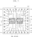
- FIG. 1 illustrates a plan view showing a semiconductor package according to exemplary embodiments of inventive concepts.
- FIG. 2A illustrates a cross-sectional view taken along line I-I' of FIG. 1 , showing a semiconductor package according to exemplary embodiments of inventive concepts.
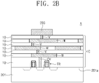
- FIG. 2B illustrates an enlarged view showing section A of FIG. 2A .
- a semiconductor package 1000 may include a package substrate 100, a first semiconductor chip 200, a second semiconductor chip 300a, a third semiconductor chip 300b, and a molding layer 400.
- the first semiconductor chip 200 may be disposed on the package substrate 100.
- the package substrate 100 may be or include, for example, a printed circuit board (PCB).
- the package substrate 100 may include first pads 101 and second pads 103.
- the first pads 101 and the second pads 103 may be disposed on a top surface of the package substrate 100.
- the first pads 101 may be spaced apart from each other in a first direction and a second direction intersecting the first direction.
- the second pads 103 may be spaced apart from each other along an edge of the package substrate 100.
- External terminals 105 may be disposed on a bottom surface of the package substrate 100, which the bottom surface is opposite to the top surface of the package substrate 100.
- the external terminals 105 may be attached onto the bottom surface of the package substrate 100.
- the external terminals 105 may electrically connect the package substrate 100 to an external apparatus.
- the external terminals 105 may include, for example, solder bumps or solder balls.
- the first semiconductor chip 200 may include a substrate (e.g., a chip substrate) 201, an integrated circuit region IC, first chip pads 203, second chip pads 205, a first insulation layer 207, redistribution lines 209, and a second insulation layer 211.
- the substrate 201 may be or include, for example, a silicon substrate, a germanium substrate, or a silicon-germanium substrate.
- the substrate 201 may have a first surface 201a and a second surface 201b opposite to the first surface 201a.
- the substrate 201 may be configured in such a way that the first surface 201a is closer than the second surface 201b to the package substrate 100.
- the integrated circuit region IC may be disposed in the substrate 201 and on the first surface 201a of the substrate 201.
- the integrated circuit region IC may include a plurality of internal circuits.
- the internal circuits may include transistors TR disposed in the substrate 201 and on the first surface 201a of the substrate 201, a contact via CV, a plurality of interlayer dielectric layers 10 sequentially stacked on the first surface 201a of the substrate 201, metal lines M disposed in the interlayer dielectric layers 10, and vias V that penetrate the interlayer dielectric layers 10 and electrically connect the metal lines M disposed in different interlayer dielectric layers 10.
- the internal circuits may include at least one of a driver circuit, a receiver circuit, a transceiver circuit, a control circuit, a power circuit, etc.
- the contact via CV may electrically connect at least one transistor TR (e.g., a source/drain region thereof) to the metal lines M.
- the transistors TR may be constituent parts of a control circuit and/or a power circuit.
- the first semiconductor chip 200 may be a semiconductor logic chip.
- the first chip pads 203 may be disposed on the first surface 201a of the substrate 201.
- the first chip pads 203 may be disposed on the interlayer dielectric layer 10 at the top level from the first surface 201a of the substrate 201.
- the first chip pads 203 may be spaced apart from each other in the first direction and the second direction intersecting the first direction.
- the first chip pads 203 may be in contact with internal circuits in the integrated circuit region IC.
- the first chip pads 203 may be electrically connected to the transistors TR.
- each of the first chip pads 203 may be electrically connected to at least one transistor TR through the vias V, the metal lines M, and the contact via CV.
- the second chip pads 205 may be disposed on the second surface 201b of the substrate 201. In some examples, the second chip pads 205 may be disposed on and may contact a portion of the redistribution lines 209. The second chip pads 205 may be spaced apart from each other in the first direction and the second direction intersecting the first direction. In the first semiconductor chip 200, the second chip pads 205 may be spaced apart from the integrated circuit region IC. For example, in the first semiconductor chip 200, the second chip pads 205 may not be electrically connected to the transistors TR of the integrated circuit region IC.
- the first insulation layer 207 may be disposed on the second surface 201b of the substrate 201.
- the first insulation layer 207 may cover the second surface 201b of the substrate 201 and expose top surfaces of the second chip pads 205.
- the first insulation layer 207 may cover the second surface 201b of the substrate 201 and expose top surfaces of the redistribution lines 209.
- the first insulation layer 207 may include a single layer or a plurality of layers.
- the first insulation layer 207 may include, for example, one or more of a silicon oxide layer, a silicon nitride layer, and a silicon oxynitride layer.
- the redistribution lines 209 may be disposed on the second surface 201b of the substrate 201.
- the redistribution lines 209 may be spaced apart from each other.
- the redistribution lines 209 may partially cover a top surface of the first insulation layer 207.
- the redistribution lines 209 may be correspondingly electrically connected to the second chip pads 205.
- the redistribution lines 209 may contact and be electrically connected to the second chip pads 205 in one-to-one correspondence.
- the redistribution lines 209 On the second surface 201b of the substrate 201, the redistribution lines 209 may have linear shapes extending from the second chip pads 205 toward side surfaces of the substrate 201.
- each of the redistribution lines 209 may have one end in contact with the second chip pad 205 and other end adjacent to the side surface of the substrate 201.
- the other ends of the redistribution lines 209 may be spaced apart from the second chip pads 205 and positioned on an edge of the substrate 201.
- the redistribution lines 209 may each include a single metal layer or a plurality of metal layers.
- the redistribution lines 209 may include, for example, one or more of aluminum (Al), nickel (Ni), and copper (Cu).
- the redistribution lines 209 may be spaced apart from the integrated circuit region IC.
- the redistribution lines 209 may not be electrically connected to the transistors TR of the integrated circuit region IC.
- FIG. 1 exemplarily shows the number and arrangement of the redistribution lines 209, but inventive concepts are not limited to that shown.
- an active surface of the first semiconductor chip 200 may include one surface of each of the first chip pads 203, and an inactive surface of the first semiconductor chip 200 may include one surface of each of the second chip pads 205 and one surface of each of the redistribution lines 209.
- the active surface of the first semiconductor chip 200 may represent a first surface on which the first chip pads 203 electrically connected to the internal circuits of the integrated circuit region IC are disposed and the inactive surface of the first semiconductor chip 200 may represent a second surface opposite to the first surface on which the second chip pads 205 not electrically connected to the internal circuits of the integrated circuit region IC are disposed.
- the first chip pads 203 may be formed adjacent to the internal circuits of the integrated circuit region IC, and the second chip pads 205 may be formed spaced apart from the internal circuits of the integrated circuit region IC.
- the second insulation layer 211 may be disposed on the redistribution lines 209 and the first insulation layer 207.
- the second insulation layer 211 may partially expose the redistribution lines 209.
- the second insulation layer 211 may expose the other ends of the redistribution lines 209 and the one ends of the redistribution lines 209, which the one ends are in contact with the second chip pads 205.
- the second insulation layer 211 may expose the second chip pads 205 and the other ends of the redistribution lines 209, which the other ends are disposed adjacent to the side surfaces of the substrate 201.
- the second insulation layer 211 may include a single layer or a plurality of layers.
- the second insulation layer 211 may include, for example, a silicon oxide layer, a silicon nitride layer, or a silicon oxynitride layer.
- Bonding wires 230 may be disposed between the other ends of the redistribution lines 209 and the second pads 103 of the package substrate 100, thereby electrically connecting the redistribution lines 209 to the second pads 103.
- the package substrate 100 and the first semiconductor chip 200 may not be electrically connected to each other through the bonding wires 230.
- the bonding wires 230 may include, for example, gold (Au).
- the package substrate 100 and the first semiconductor chip 200 may be provided therebetween with terminals (or, connection members) 240.
- the terminals 240 may be disposed between the first chip pads 203 and the first pads 101.
- the terminals 240 may be in contact with the first chip pads 203.
- the terminals 240 may be electrically connected to the internal circuits of the integrated circuit region IC (e.g., transistors TR).
- the terminals 240 may electrically connect the first semiconductor chip 200 to the package substrate 100.
- the second semiconductor chip 300a and the third semiconductor chip 300b may be disposed on the first semiconductor chip 200.
- the second and third semiconductor chips 300a and 300b may be disposed on the second surface 201b of the substrate 201.
- the second and third semiconductor chips 300a and 300b may be horizontally spaced apart from each other.
- Each of the second and third semiconductor chips 300a and 300b may vertically overlap the second chip pads 205.
- Each of the second and third semiconductor chips 300a and 300b may include one surface 301 and other surface 302 opposite to the one surface 301.
- the one surface 301 of each of the second and third semiconductor chips 300a and 300b may be closer than the other surface 302 to the first semiconductor chip 200.
- the second and third semiconductor chips 300a and 300b may be semiconductor memory chips.
- Connection members (or, terminals) 310 may be disposed between the first semiconductor chip 200 and each of the second and third semiconductor chips 300a and 300b.
- connection members 310 may be disposed between the second chip pads 205 and the one surface 301 of each of the second and third semiconductor chips 300a and 300b.
- Each connection members 310 may contact the one end of a redistribution line 209.
- the connection members 310 may contact the second chip pads 205.
- the connection members 310 may be, for example, solder bumps or solder balls.
- the second and third semiconductor chips 300a and 300b may be electrically connected to the package substrate 100 through the connection members 310, the redistribution lines 209, and the bonding wires 230. In some examples, the second and third semiconductor chips 300a and 300b may be electrically connected to the package substrate 100 through the connection members 310, the second chip pads 205, the redistribution lines 209, and the bonding wires 230. In some embodiments, the second and third semiconductor chips 300a and 300b may be electrically connected to the transistors TR of the first semiconductor chip 200 through the connection members 310, the redistribution lines 209, the bonding wires 230, and the package substrate 100.
- the second and third semiconductor chips 300a and 300b may be electrically connected to the transistors TR of the first semiconductor chip 200 through the connection members 310, the second chip pads 205, the redistribution lines 209, the bonding wires 230, and the package substrate 100.
- the transistors TR disposed on the first semiconductor chip 200 may drive internal circuits included in the second and third semiconductor chips 300a and 300b.
- the first semiconductor chip 200 may be electrically connected to the second and third semiconductor chips 300a and 300b through the connection members 310, the redistribution lines 209, and the bonding wires 230 (and optionally may include the second chip pads 205), without any other structures between the first semiconductor chip 200 and each of the second and third semiconductor chips 300a and 300b. Accordingly, a minimal transmission distance may be achieved between the first semiconductor chip 200 and the second semiconductor chip 300a and between the first semiconductor chip 200 and the third semiconductor chip 300b. In addition, the first semiconductor chip 200 may easily radiate heat generated therefrom.
- the molding layer 400 may be disposed on the package substrate 100.
- the molding layer 400 may cover the bonding wires 230 and the first, second, and third semiconductor chips 200, 300a, and 300b, and may be disposed in a space between the package substrate 100 and the first semiconductor chip 200, a space between the first semiconductor chip 200 and the second semiconductor chip 300a, and a space between the first semiconductor chip 200 and the third semiconductor chip 300b.
- the molding layer 400 may include an insulating polymeric material such as an epoxy molding compound.
- FIG. 3 illustrates a cross-sectional view taken along line I-I' of FIG. 1 , showing a semiconductor package according to exemplary embodiments of inventive concepts.
- FIGS. 1 , 2A , and 2B show a cross-sectional view taken along line I-I' of FIG. 1 , showing a semiconductor package according to exemplary embodiments of inventive concepts.
- a semiconductor package 2000 may include a package substrate 100, a first semiconductor chip 200, a second semiconductor chip 300a, a third semiconductor chip 300b, a plurality of fourth semiconductor chips 600, and a molding layer 400.
- Each of the second and third semiconductor chips 300a and 300b may include through vias 320.
- the through vias 320 may be disposed within the second and third semiconductor chips 300a and 300b.
- the plurality of the fourth semiconductor chips 600 may be vertically stacked on each of the second and third semiconductor chips 300a and 300b.
- Other through vias 320 may be included in the fourth semiconductor chips 600, but not in top ones of the fourth semiconductor chips 600.
- the through vias 320 may be disposed within the fourth semiconductor chips 600.
- the plurality of the fourth semiconductor chips 600 may be semiconductor memory chips.
- Solder balls 330 may be disposed in a space between the second semiconductor chip 300a and its overlying fourth semiconductor chip 600, a space between the third semiconductor chip 300b and its overlying fourth semiconductor chip 600, and spaces between the fourth semiconductor chips 600 vertically adjacent to each other.
- the second semiconductor chip 300a and the fourth semiconductor chips 600, which chips 300a and 600 vertically overlap each other, may be electrically connected to each other through the solder balls 330 and the through vias 320
- the third semiconductor chip 300b and the fourth semiconductor chips 600, which chips 300b and 600 vertically overlap each other may be electrically connected to each other through the solder balls 330 and the through vias 320.
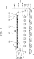
- FIG. 4 illustrates a plan view showing a semiconductor package 3000 according to exemplary embodiments of inventive concepts.
- FIG. 5 illustrates a cross-sectional view taken along line II-II' of FIG. 4 , showing a semiconductor package according to exemplary embodiments of inventive concepts.
- FIG. 4 omits the second chip pads 205 shown in FIG. 1 .
- an adhesive layer 340 may be interposed between a first semiconductor chip 200 and each of second and third semiconductor chips 300a and 300b.
- the second semiconductor chip 300a and the third semiconductor chip 300b may be adhered through the adhesive layer 340 onto the first semiconductor chip 200.
- the adhesive layer 340 may be in contact with one surface 301 of each of the second and third semiconductor chips 300a and 300b, one ends of redistribution lines 209, and a portion of a second insulation layer 211.
- the adhesive layer 340 may be in contact with one surface 301 of each of the second and third semiconductor chips 300a and 300b, second chip pads 205, and a portion of a second insulation layer 211.
- the adhesive layer 340 may be, for example, an epoxy, a silicon-based insulation layer, or a tape.
- Each of the second and third semiconductor chips 300a and 300b may include a first side surface 303, a second side surface 304, a third side surface 305, and a fourth side surface 306.
- the first side surface 303 of the second semiconductor chip 300a may be adjacent to the third semiconductor chip 300b
- the first side surface 303 of the third semiconductor chip 300b may be adjacent to the second semiconductor chip 300a.
- the first side surfaces 303 of the second and third semiconductor chips 300a and 300b may be adjacent to and face each other.
- Third chip pads 350 may be disposed on other surface 302 of each of the second and third semiconductor chips 300a and 300b.
- the third chip pads 350 may be disposed on the other surface (e.g., an active surface) 302 of each of the second and third semiconductor chips 300a and 300b.
- the active surface 302 of each of the second and third semiconductor chips 300a and 300b may be electrically connected to internal circuits of each of the second and third semiconductor chips 300a and 300b.
- each of the second and third semiconductor chips 300a and 300b may include the one surface, for example, an inactive surface 301 on which internal circuits are not disposed.
- the third chip pads 350 When viewed in plan, on the other surface 302 of each of the second and third semiconductor chips 300a and 300b, the third chip pads 350 may be arranged along the second, third, and fourth side surfaces 304, 305, and 306. On the other surface 302 of each of the second and third semiconductor chips 300a and 300b, the third chip pads 350 may not be arranged along the first side surface 303. For example, on the other surface 302 of each of the second and third semiconductor chips 300a and 300b, the third chip pads 350 may be adjacent to the second, third, and fourth side surfaces 304, 305, and 306 except for the first side surface 303. However, FIG.
- the third chip pads 350 exemplarily shows the third chip pads 350 arranged along the second, third, and fourth side surfaces 304, 305, and 306, but inventive concepts are not limited to that shown.
- the third chip pads 350 may be arranged along the first, second, third, and fourth side surfaces 303, 304, 305, and 306.
- Connection members 310 may be disposed between other ends of the redistribution lines 209 and the other surface 302 of each of the second and third semiconductor chips 300a and 300b. When viewed in plan, the connection members 310 may be disposed between the third chip pads 350 and the other ends of the redistribution lines 209, while crossing over at least one of the first, second, third, and fourth side surfaces 303, 304, 305, and 306 of each of the second and third semiconductor chips 300a and 300b. The connection members 310 may be in contact with the third chip pads 350 and the other ends of the redistribution lines 209. The connection members 310 may be, for example, bonding wires.
- connection members 310 may neither cross over nor lie on all of the first, second, third, and fourth side surfaces 303, 304, 305, and 306 of each of the second and third semiconductor chips 300a and 300b.
- connection members 310 may connect the third chip pads 350 to the other ends of the redistribution lines 209, while crossing over the second, third, and fourth side surfaces 304, 305, and 306 of the second semiconductor chip 300a.
- the connection members 310 may not cross over the first side surface 303 of the second semiconductor chip 300a.
- the connection members 310 may connect the third chip pads 350 to the other ends of the redistribution lines 209, while crossing over the second, third, and fourth side surfaces 304, 305, and 306 of the third semiconductor chip 300b.
- the connection members 310 may not cross over the first side surface 303 of the third semiconductor chip 300b.
- FIG. 6 illustrates a cross-sectional view taken along line II-II' of FIG. 4 , showing a semiconductor package 4000 including a plurality of fourth semiconductor chips 600 according to exemplary embodiments of inventive concepts.
- FIG. 6 illustrates a cross-sectional view taken along line II-II' of FIG. 4 , showing a semiconductor package 4000 including a plurality of fourth semiconductor chips 600 according to exemplary embodiments of inventive concepts.
- a second insulation layer 211 may be disposed on redistribution lines 209 and a first insulation layer 207.
- the second insulation layer 211 may be disposed on the redistribution lines 209, second chip pads 205, and a first insulation layer 207.
- the second insulation layer 211 may cover the second chip pads 205, the first insulation layer 207, and portions of the redistribution lines 209.
- the second insulation layer 211 may partially expose other ends of the redistribution lines 209.
- An adhesive layer 340 may be interposed between a first semiconductor chip 200 and each of second and third semiconductor chips 300a and 300b.
- the second semiconductor chip 300a and the third semiconductor chip 300b may be adhered through the adhesive layer 340 onto the first semiconductor chip 200.
- the adhesive layer 340 may be in contact with the second insulation layer 211 and one surface 301 of each of the second and third semiconductor chips 300a and 300b.
- Connection members 310 may disposed between and electrically connect the other ends of the redistribution lines 209 and other surface 302 of each of the second and third semiconductor chips 300a and 300b.
- a plurality of fourth semiconductor chips 600 may be vertically stacked on each of the second and third semiconductor chips 300a and 300b.
- the fourth semiconductor chips 600 vertically stacked may be adhered to each other through at least one adhesive layer 340.
- the adhesive layer 340 may be provided to attach one or more chips 600 of the plurality of fourth semiconductor chips 600 onto their underlying second semiconductor chip 300a, and the adhesive layer 340 may be provided to attach one or more chips 600 of the plurality of fourth semiconductor chips 600 onto their underlying third semiconductor chip 300b.
- the fourth semiconductor chips 600 stacked on the second semiconductor chip 300a may be sequentially offset to expose third chip pads 350 and fourth chip pads 360 disposed on top surfaces of the second semiconductor chip 300a and the fourth semiconductor chips 600, respectively.
- the fourth semiconductor chips 600 stacked on the second semiconductor chip 300a may be sequentially offset toward the fourth semiconductor chips 600 stacked on the third semiconductor chip 300b.
- the fourth semiconductor chips 600 stacked on the third semiconductor chip 300b may be sequentially offset to expose the third chip pads 350 and the fourth chip pads 360 disposed on the top surfaces of the third semiconductor chip 300b and the fourth semiconductor chips 600, respectively.
- the fourth semiconductor chips 600 stacked on the third semiconductor chip 300b may be sequentially offset toward the fourth semiconductor chips 600 stacked on the second semiconductor chip 300a.
- First bonding wires 370 may electrically connect the third and fourth chip pads 350 and 360 that are vertically adjacent to each other, and also electrically connect the fourth chip pads 360 that are vertically adjacent to each other.
- FIG. 7 illustrates a plan view showing a semiconductor package 5000 according to exemplary embodiments of inventive concepts.
- FIG. 8 illustrates a cross-sectional view taken along line 111-111' of FIG. 7 , showing a semiconductor package 5000 according to exemplary embodiments of inventive concepts.
- FIG. 7 omits the second chip pads 205 shown in FIG. 1 .
- a semiconductor package 5000 may include a package substrate 100, a first semiconductor chip 200, a second semiconductor chip 300, and a molding layer 400.
- the second semiconductor chip 300 may be disposed on the first semiconductor chip 200.
- An adhesive layer 340 may be interposed between the first semiconductor chip 200 and the second semiconductor chip 300, and thus may attach the second semiconductor chip 300 onto the first semiconductor chip 200.
- the second semiconductor chip 300 may be a semiconductor memory chip.
- Third chip pads 350 may be disposed on other surface 302 (e.g., an active surface) of the second semiconductor chip 300.
- the third chip pads 350 may be arranged along side surfaces of the second semiconductor chip 300.
- the third chip pads 350 may be arranged along a first side surface 303, a second side surface 304, a third side surface 305, and a fourth side surface 306 of the second semiconductor chip 300.
- Connection members 310 may be disposed between the other surface 302 of the second semiconductor chip 300 and other ends of redistribution lines 209.
- the connection members 310 may be in contact with the third chip pads 350 and the other ends of the redistribution lines 209.
- the connection members 310 may be, for example, bonding wires. When viewed in plan, the connection members 310 may connect the third chip pads 350 to the other ends of the redistribution lines 209, while crossing over the first, second, third, and fourth side surfaces 303, 304, 305, and 306 of the second semiconductor chip 300.
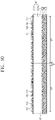
- FIGS. 9A to 9H illustrate cross-sectional views showing a method of fabricating a semiconductor package according to exemplary embodiments of inventive concepts.
- a substrate 201 may be provided to include an integrated circuit region IC.
- the substrate 201 may be, for example, a bare wafer.
- the substrate 201 may be, for example, a silicon substrate, a germanium substrate, or a silicon-germanium substrate.
- the substrate 201 may have a first surface 201a and a second surface 201b opposite to each other.
- the substrate 201 may include device regions DR spaced apart from each other in a first direction and a second direction intersecting the first direction, and also include a scribe region SR defining the device regions DR.
- the device regions DR of the substrate 201 may be areas where semiconductor chips are formed.
- the integrated circuit region IC may be formed in each of the device regions DR of the substrate 201.
- the integrated circuit region IC may be formed in the substrate 201 and on the first surface 201a of the substrate 201.
- the integrated circuit region IC may include transistors TR, a plurality of interlayer dielectric layers 10, metal lines M, a contact via CV, and vias VI.
- the transistors TR may be provided in the substrate 201 and on the first surface 201a of the substrate 201.
- the transistors TR may be constituent parts of a control circuit, a driver circuit, a receiver circuit, a transceiver circuit, and/or a power circuit.
- the plurality of interlayer dielectric layers 10 may be sequentially formed on the first surface 201a of the substrate 201.
- the metal lines M may be formed on and between the plurality of interlayer dielectric layers 10.
- the vias V may be formed between the plurality of interlayer dielectric layers 10, and may electrically connect the metal lines M formed on different interlayer dielectric layers 10.
- the contact via CV may electrically connect at least one transistor TR (e.g., a source/drain region thereof) to the metal lines M.
- First chip pads 203 may be formed in the device regions DR of the substrate 201.
- the first chip pads 203 may be formed on the first surface 201a (i.e., an active surface) of the substrate 201.
- the first chip pads 203 may be formed on a top one of the interlayer dielectric layers 10 on the integrated circuit region IC.
- the first chip pads 203 may be formed spaced apart from each other in the first direction and the second direction intersecting the first direction.
- Terminals 240 may be formed on the first chip pads 203.
- the terminals 240 may be electrically connected to the first chip pads 203.
- the terminals 240 may include, for example, one or more of copper (Cu), silver (Ag), platinum (Pt), aluminum (Al), and copper (Cu).
- the terminals 240 may be formed by a sputtering process, a plating process such as pulse plating or direct-current plating, a soldering process, or an attach process.
- a supporter 500 may be provided on the first surface 201a of the substrate 201.
- the supporter 500 may cover the first chip pads 203 and the terminals 240.
- the supporter 500 may be a wafer supporting system for handling the substrate 201.
- the supporter 500 may include an adhesive material, for example, an epoxy, a silicon-based insulation layer, or a tape.
- second chip pads 205 may be formed in the device regions DR of the substrate 201.
- the second chip pads 205 may be formed on the second surface 201b (i.e., an inactive surface) of the substrate 201.
- the second chip pads 205 may be formed spaced apart from each other in the first direction and the second direction intersecting the first direction.
- a first insulation layer 207 may be formed on the second surface 201b of the substrate 201.
- the first insulation layer 207 may be formed by forming and patterning an insulation layer (not shown) covering the second chip pads 205 and the second surface 201b of the substrate 201. When the insulation layer is patterned, top surfaces of the second chip pads 205 may be exposed by the first insulation layer 207.
- the first insulation layer 207 may be formed of a single layer or a plurality of layers.
- the first insulation layer 207 may include, for example, one or more of a silicon oxide layer, a silicon nitride layer, and a silicon oxynitride layer.
- a metal layer 510 may be formed on the second surface 201b of the substrate 201.
- the metal layer 510 may be formed to cover the top surfaces of the second chip pads 205 and a top surface of the first insulation layer 207.
- the metal layer 510 may be formed of a single layer or a plurality of layers.
- the metal layer 510 may include, for example, one or more of aluminum (Al), nickel (Ni), and copper (Cu).
- Photoresist patterns PR may be formed on the metal layer 510.
- the photoresist patterns PR may partially expose the metal layer 510.
- the photoresist patterns PR may be shaped the same as the redistribution lines 209 discussed above with reference to FIGS. 1 and 2A .
- the photoresist patterns PR may be used as an etching mask to partially etch the metal layer 510, which may result in forming redistribution lines 209.
- the metal layer 510 may be partially etched to expose portions of the top surface of the first insulation layer 207.
- a dry or wet etching process may be adopted as the etching process.
- the redistribution lines 209 may be formed in the device regions DR of the substrate 201. As illustrated in FIG. 1 , the redistribution lines 209 may be formed to correspond to the second chip pads 205.
- the redistribution lines 209 may have linear shapes extending from the second chip pads 205 toward the scribe region SR of the substrate 201.
- the redistribution lines 209 may have one ends in contact respectively with the top surfaces of the second chip pads 205.
- the redistribution lines 209 may have other ends adjacent to the scribe region SR of the substrate 201. After the etching process, the photoresist patterns PR may be removed.
- a second insulation layer 211 may be formed on the second surface 201b of the substrate 201.
- the second insulation layer 211 may be formed to cover the redistribution lines 209 and the top surface of the first insulation layer 207, which top surface is exposed by the redistribution lines 209.
- the second insulation layer 211 may be formed of a single layer or a plurality of layers.
- the second insulation layer 211 may include, for example, one or more of a silicon oxide layer, a silicon nitride layer, and a silicon oxynitride layer.
- an etching process may be performed on the second insulation layer 211, thereby exposing the one and other ends of the redistribution lines 209.
- an etching mask pattern (not shown) may be formed on the second insulation layer 211, and the second insulation layer 211 may be etched on its portions exposed by the etching mask pattern.
- the second insulation layer 211 may cover remaining portions of the redistribution lines 209 except for the one and other ends of the redistribution lines 209.
- a cutting process may be performed along the scribe region SR of the substrate 201.
- the cutting process may sequentially cut the second insulation layer 211, the first insulation layer 207, and the supporter 500 that are formed on the scribe region SR of the substrate 201. Therefore, a plurality of first semiconductor chips 200 may be formed.
- Each of the first semiconductor chips 200 may include a substrate 201, the integrated circuit region IC, the first chip pads 203, the second chip pads 205, the first insulation layer 207, the redistribution lines 209, and the second insulation layer 211.
- the first semiconductor chips 200 may be semiconductor logic chips.
- a removal process may be performed on the supporter 500 covering the terminals 240 and the first chip pads 203.
- the supporter 500 may be removed before the cutting process.
- the redistribution lines 209 may be formed before forming the second chip pads 205.
- the second chip pads 205 may be disposed on first ends of the redistribution lines 209.
- the second insulation layer 211 may be formed to cover some portions of the redistribution lines 209, the second chip pads 205, and the top surface of the first insulation layer 207, which top surface is exposed by the redistribution lines 209, and referring to FIG. 9F , an etching process may be performed on the second insulation layer 211, thereby exposing second ends of the redistribution lines 209.
- an etching mask pattern (not shown) may be formed on the second insulation layer 211, and the second insulation layer 211 may be etched on its portions exposed by the etching mask pattern.
- the second insulation layer 211 may cover the second chip pads 205 and the remaining portions of the redistribution lines 209 except for the second ends of the redistribution lines 209.
- a package substrate 100 may be prepared.
- the package substrate 100 may be, for example, a printed circuit board (PCB).
- the package substrate 100 may include first pads 101 and second pads 103.
- the first pads 101 and the second pads 103 may be disposed on a top surface of the package substrate 100.
- External terminals 105 may be formed on a bottom surface of the package substrate 100.
- the external terminals 105 may include solder balls or solder bumps.
- the formation order of the external terminals 105 is not be limited to the mentioned above.
- the first semiconductor chip 200 may be stacked on the package substrate 100.
- the terminals 240 may be disposed to correspond to the first pads 101.
- the first semiconductor chip 200 may be mounted on the package substrate 100 in a flip-chip bonding manner.
- a second semiconductor chip 300a and a third semiconductor chip 300b may be stacked on the first semiconductor chip 200.
- Connection members 310 formed on one surface 301 of each of the second and third semiconductor chips 300a and 300b may be disposed to correspond to one ends of the redistribution lines 209 and the top surfaces of the second chip pads 205.
- the second and third semiconductor chips 300a and 300b may be mounted on the first semiconductor chip 200 in a flip-chip bonding manner.
- the connection members 310 may include, for example, solder bumps or solder balls.
- the second and third semiconductor chips 300a and 300b may be mounted on the first semiconductor chip 200 in a wire bonding manner.
- the connection members 310 may include, for example, bonding wires.
- the second and third semiconductor chips 300a and 300b may be semiconductor memory chips.
- Bonding wires 230 may be formed between the package substrate 100 and the second surface 201b of the substrate 201.
- the bonding wires 230 may be formed to extend from other ends of the redistribution lines 209 onto the second pads 103 of the package substrate 100.
- the bonding wires 230 may include, for example, gold (Au).
- a molding layer 400 may be formed on the package substrate 100.
- the molding layer 400 may cover the first semiconductor chip 200, the second semiconductor chip 300a, the third semiconductor chip 300b, and the bonding wires 230, and may fill a space between the package substrate 100 and the first semiconductor chip 200, a space between the first semiconductor chip 200 and the second semiconductor chip 300a, and a space between the first semiconductor chip 200 and the third semiconductor chip 300b.
- the molding layer 400 may include, for example, an insulating polymeric material such as an epoxy molding compound.
- a first semiconductor chip and a second semiconductor chip sequentially stacked on a package substrate may be electrically connected to each other through connection members that electrically connect the first and second semiconductor chips to each other, through redistribution lines that are in contact with the connection members and disposed on one surface (e.g., an inactive surface) of the first semiconductor chip adjacent to the second semiconductor chip, and through bonding wires between the redistribution lines and the package substrate, without any other additional structures between the first and second semiconductor chips. Accordingly, it may be possible to minimize or reduce a transmission distance between the first and second semiconductor chips and to easily radiate heat generated in the first semiconductor chip.
Landscapes
- Production Of Multi-Layered Print Wiring Board (AREA)
- Semiconductor Integrated Circuits (AREA)
- Structures Or Materials For Encapsulating Or Coating Semiconductor Devices Or Solid State Devices (AREA)
- Engineering & Computer Science (AREA)
- Manufacturing & Machinery (AREA)
- Internal Circuitry In Semiconductor Integrated Circuit Devices (AREA)
Claims (8)
- Halbleitergehäuse (1000), aufweisend:ein Gehäusesubstrat (100);einen ersten Halbleiterchip (200) auf dem Gehäusesubstrat (100); undeinen zweiten Halbleiterchip (300a) auf dem ersten Halbleiterchip (200), wobei der erste Halbleiterchip (200) aufweist:ein Chipsubstrat (201), das eine erste Oberfläche und eine zweite Oberfläche, die der ersten Oberfläche gegenüberliegt, enthält;eine Mehrzahl an ersten Chip-Pads (203) zwischen dem Gehäusesubstrat (100) und dem Chipsubstrat (201), die den ersten Halbleiterchip (200) mit dem Gehäusesubstrat (100) elektrisch verbinden;eine Mehrzahl an zweiten Chip-Pads (205), die auf der zweiten Oberfläche und zwischen dem zweiten Halbleiterchip (300a) und der zweiten Oberfläche angeordnet sind;eine Mehrzahl an Umverteilungslleitungen (209) auf der zweiten Oberfläche, wobei die Umverteilungslleitungen (209) den zweiten Halbleiterchip (300a) elektrisch verbinden; undeine Mehrzahl an ersten Bonddrähten (230), welche die Umverteilungslleitungen (209) mit dem Gehäusesubstrat (100) elektrisch verbinden,dadurch gekennzeichnet, dassder zweite Halbleiterchip (300a) ferner eine Durchkontaktierung (320) aufweist, die den zweiten Halbleiterchip (300a) durchdringt, unddadurch, dass das Halbleitergehäuse (100) ferner aufweist:einen dritten Halbleiterchip (600) auf dem zweiten Halbleiterchip (300a), wobei der dritte Halbleiterchip (600) durch die Durchkontaktierung (320) mit dem ersten Halbleiterchip (200) elektrisch verbunden ist; undeine Lötkugel, die mit der Durchkontaktierung (320) zwischen dem zweiten Halbleiterchip (300a) und dem dritten Halbleiterchip (600) elektrisch verbunden ist.
- Halbleitergehäuse nach Anspruch 1, wobei die Mehrzahl an zweiten Chip-Pads (205) den zweiten Halbleiterchip (300a) vertikal überlappt, und
wobei die Umverteilungsleitungen (209) jeweils mit den zweiten Chip-Pads (205) verbunden sind. - Halbleitergehäuse nach Anspruch 2, wobei der zweite Halbleiterchip (300a) eine erste Oberfläche, die benachbart zum ersten Halbleiterchip (200) ist, und eine zweite Oberfläche, die der ersten Oberfläche gegenüberliegt, enthält, und
wobei die Umverteilungsleitungen (209) durch eine Mehrzahl an Verbindungselementen (240), die zwischen den zweiten Chip-Pads (205) und der ersten Oberfläche des zweiten Halbleiterchips (300a) angeordnet sind, mit dem zweiten Halbleiterchip (300a) elektrisch verbunden sind. - Halbleitergehäuse nach Anspruch 2, wobei:sich die Umverteilungsleitungen (209) von den zweiten Chip-Pads (205) in Richtung von Seitenoberflächen des Chipsubstrats (201) erstrecken,erste Enden der Umverteilungsleitungen (209) mit den zweiten Chip-Pads (205) in Berührung sind, undauf der zweiten Oberfläche des Chipsubstrats (201) zweite Enden der Umverteilungsleitungen (209), die den ersten Enden gegenüberliegen, benachbart zu den Seitenoberflächen des Chipsubstrats (201) sind.
- Halbleitergehäuse nach Anspruch 4, wobei der zweite Halbleiterchip (300a) eine erste Oberfläche, die benachbart zum ersten Halbleiterchip (200) ist, und eine zweite Oberfläche, die der ersten Oberfläche gegenüberliegt, enthält, und
wobei die Umverteilungsleitungen (209) durch eine Mehrzahl an Verbindungselementen, die zwischen der zweiten Oberfläche des zweiten Halbleiterchips (300a) und den zweiten Enden der Umverteilungsleitungen (209) angeordnet sind, mit dem zweiten Halbleiterchip (300a) elektrisch verbunden sind. - Halbleitergehäuse nach Anspruch 1, wobei der erste Halbleiterchip (200) ferner einen integrierten Schaltungsbereich (IC) aufweist, der benachbart zu der ersten Oberfläche des Chipsubstrats (201) ist,wobei eine interne Schaltung, die im integrierten Schaltungsbereich enthalten ist, mit einem entsprechenden Chip-Pad der ersten Chip-Pads (203) elektrisch verbunden ist, undwobei die Umverteilungsleitungen (209) vom integrierten Schaltungsbereich (IC) beabstandet sind.
- Halbleitergehäuse nach Anspruch 1, ferner aufweisend eine Mehrzahl an Anschlüssen (105), die zwischen dem Gehäusesubstrat (100) und der ersten Oberfläche des Chipsubstrats (201) angeordnet sind und den ersten Halbleiterchip (200) durch die ersten Chip-Pads (203) mit dem Gehäusesubstrat (100) elektrisch verbinden.
- Halbleitergehäuse nach Anspruch 1, wobei die Umverteilungsleitungen (209) durch Verbindungselemente (240), die Lötkugeln, Lötkontakthöcker oder Bonddrähte enthalten, mit dem zweiten Halbleiterchip (300a) elektrisch verbunden sind.
Applications Claiming Priority (1)
| Application Number | Priority Date | Filing Date | Title |
|---|---|---|---|
| KR1020180034454A KR102589736B1 (ko) | 2018-03-26 | 2018-03-26 | 반도체 칩 및 이를 포함하는 반도체 패키지 |
Publications (2)
| Publication Number | Publication Date |
|---|---|
| EP3547364A1 EP3547364A1 (de) | 2019-10-02 |
| EP3547364B1 true EP3547364B1 (de) | 2022-04-20 |
Family
ID=65013524
Family Applications (1)
| Application Number | Title | Priority Date | Filing Date |
|---|---|---|---|
| EP19150914.0A Active EP3547364B1 (de) | 2018-03-26 | 2019-01-09 | Halbleiterchip und halbleitergehäuse damit |
Country Status (4)
| Country | Link |
|---|---|
| US (1) | US10748871B2 (de) |
| EP (1) | EP3547364B1 (de) |
| KR (1) | KR102589736B1 (de) |
| CN (1) | CN110364513B (de) |
Families Citing this family (10)
| Publication number | Priority date | Publication date | Assignee | Title |
|---|---|---|---|---|
| US11824009B2 (en) * | 2018-12-10 | 2023-11-21 | Preferred Networks, Inc. | Semiconductor device and data transferring method for semiconductor device |
| KR102749207B1 (ko) * | 2019-12-06 | 2025-01-06 | 삼성전자주식회사 | 반도체 패키지 및 그의 제조 방법 |
| KR102813432B1 (ko) | 2020-05-12 | 2025-05-27 | 스템코 주식회사 | 반도체 소자, 회로 기판 및 이들을 구비하는 반도체 패키지 |
| KR102877210B1 (ko) | 2020-06-22 | 2025-10-28 | 삼성전자주식회사 | 반도체 패키지 |
| CN111863794B (zh) * | 2020-07-28 | 2022-10-28 | 南通通富微电子有限公司 | 一种半导体封装器件 |
| US11600572B2 (en) * | 2021-03-11 | 2023-03-07 | Global Unichip Corporation | Routing structure between dies and method for arranging routing between dies |
| JP2024541923A (ja) * | 2021-10-25 | 2024-11-13 | アデイア セミコンダクター ボンディング テクノロジーズ インコーポレイテッド | 積層化電子デバイス用の電力分配 |
| CN114284161B (zh) * | 2021-12-23 | 2024-12-03 | 江苏中科智芯集成科技有限公司 | 半导体芯片封装方法及芯片封装结构 |
| US12588538B2 (en) * | 2023-05-24 | 2026-03-24 | Nxp B.V. | Semiconductor device having wired under bump structure and method therefor |
| KR20250087926A (ko) * | 2023-12-08 | 2025-06-17 | 삼성전자주식회사 | 메모리 장치 |
Family Cites Families (17)
| Publication number | Priority date | Publication date | Assignee | Title |
|---|---|---|---|---|
| US7034388B2 (en) * | 2002-01-25 | 2006-04-25 | Advanced Semiconductor Engineering, Inc. | Stack type flip-chip package |
| TWI268581B (en) | 2002-01-25 | 2006-12-11 | Advanced Semiconductor Eng | Stack type flip-chip package including a substrate board, a first chip, a second chip, multiple conductive wire, an underfill, and a packaging material |
| US6965160B2 (en) | 2002-08-15 | 2005-11-15 | Micron Technology, Inc. | Semiconductor dice packages employing at least one redistribution layer |
| KR100541393B1 (ko) * | 2003-04-26 | 2006-01-10 | 삼성전자주식회사 | 멀티칩 bga 패키지 |
| US7696629B2 (en) * | 2007-04-30 | 2010-04-13 | Chipmos Technology Inc. | Chip-stacked package structure |
| KR101000479B1 (ko) * | 2008-10-07 | 2010-12-14 | 박범욱 | 멀티 칩 패키지 |
| US8637983B2 (en) | 2008-12-19 | 2014-01-28 | Ati Technologies Ulc | Face-to-face (F2F) hybrid structure for an integrated circuit |
| KR101583719B1 (ko) * | 2009-07-21 | 2016-01-11 | 삼성전자주식회사 | 반도체 패키지 및 그 제조 방법 |
| JP2011061004A (ja) | 2009-09-10 | 2011-03-24 | Elpida Memory Inc | 半導体装置及びその製造方法 |
| JP5508802B2 (ja) | 2009-09-30 | 2014-06-04 | 株式会社東芝 | 半導体装置の製造方法 |
| KR20120110451A (ko) | 2011-03-29 | 2012-10-10 | 삼성전자주식회사 | 반도체 패키지 |
| JP5936968B2 (ja) | 2011-09-22 | 2016-06-22 | 株式会社東芝 | 半導体装置とその製造方法 |
| US8686570B2 (en) * | 2012-01-20 | 2014-04-01 | Taiwan Semiconductor Manufacturing Company, Ltd. | Multi-dimensional integrated circuit structures and methods of forming the same |
| WO2013153742A1 (ja) | 2012-04-11 | 2013-10-17 | パナソニック株式会社 | 半導体装置 |
| JPWO2014136156A1 (ja) * | 2013-03-08 | 2017-02-09 | パナソニック株式会社 | 半導体装置 |
| KR102530537B1 (ko) * | 2016-04-11 | 2023-05-10 | 삼성전자주식회사 | 반도체 패키지 |
| KR102570582B1 (ko) * | 2016-06-30 | 2023-08-24 | 삼성전자 주식회사 | 반도체 패키지 및 그 제조 방법 |
-
2018
- 2018-03-26 KR KR1020180034454A patent/KR102589736B1/ko active Active
- 2018-10-18 US US16/164,524 patent/US10748871B2/en active Active
-
2019
- 2019-01-09 EP EP19150914.0A patent/EP3547364B1/de active Active
- 2019-03-20 CN CN201910212737.2A patent/CN110364513B/zh active Active
Also Published As
| Publication number | Publication date |
|---|---|
| CN110364513A (zh) | 2019-10-22 |
| KR102589736B1 (ko) | 2023-10-17 |
| EP3547364A1 (de) | 2019-10-02 |
| CN110364513B (zh) | 2023-07-04 |
| US10748871B2 (en) | 2020-08-18 |
| KR20190112447A (ko) | 2019-10-07 |
| US20190295986A1 (en) | 2019-09-26 |
Similar Documents
| Publication | Publication Date | Title |
|---|---|---|
| EP3547364B1 (de) | Halbleiterchip und halbleitergehäuse damit | |
| US10734367B2 (en) | Semiconductor package and method of fabricating the same | |
| US12278222B2 (en) | Method of fabricating semiconductor package including sub-interposer substrates | |
| US9123626B1 (en) | Integrated passive flip chip package | |
| US20150325556A1 (en) | Package structure and method for fabricating the same | |
| US10978432B2 (en) | Semiconductor package | |
| KR101837514B1 (ko) | 반도체 패키지, 이의 제조 방법 및 시스템 인 패키지 | |
| US9548283B2 (en) | Package redistribution layer structure and method of forming same | |
| KR101858954B1 (ko) | 반도체 패키지 및 이의 제조 방법 | |
| KR102809407B1 (ko) | 반도체 패키지 | |
| TWI766192B (zh) | 電子封裝件及其製法 | |
| KR20220030676A (ko) | 반도체 패키지 | |
| CN117594566A (zh) | 半导体封装件 | |
| US6855573B2 (en) | Integrated circuit package and manufacturing method therefor with unique interconnector | |
| KR101037827B1 (ko) | 반도체 패키지 | |
| CN118099136A (zh) | 电子封装件及其制法 | |
| US12284758B2 (en) | Printed circuit board | |
| KR20230068687A (ko) | 반도체 패키지 및 그 제조 방법 | |
| KR20230041250A (ko) | 반도체 소자 및 이를 포함하는 반도체 패키지 | |
| US20260101735A1 (en) | Semiconductor package | |
| US20250105097A1 (en) | Semiconductor package including a dummy chip and method of manufacturing the same | |
| KR102948166B1 (ko) | 반도체 패키지 및 그 제조 방법 | |
| US20260107783A1 (en) | Semiconductor package with alignment mark and method of fabricating the same | |
| US20230090365A1 (en) | Fan-out package with antenna | |
| CN118800667A (zh) | 半导体结构及其制造方法 |
Legal Events
| Date | Code | Title | Description |
|---|---|---|---|
| PUAI | Public reference made under article 153(3) epc to a published international application that has entered the european phase |
Free format text: ORIGINAL CODE: 0009012 |
|
| STAA | Information on the status of an ep patent application or granted ep patent |
Free format text: STATUS: THE APPLICATION HAS BEEN PUBLISHED |
|
| AK | Designated contracting states |
Kind code of ref document: A1 Designated state(s): AL AT BE BG CH CY CZ DE DK EE ES FI FR GB GR HR HU IE IS IT LI LT LU LV MC MK MT NL NO PL PT RO RS SE SI SK SM TR |
|
| AX | Request for extension of the european patent |
Extension state: BA ME |
|
| STAA | Information on the status of an ep patent application or granted ep patent |
Free format text: STATUS: REQUEST FOR EXAMINATION WAS MADE |
|
| 17P | Request for examination filed |
Effective date: 20191112 |
|
| RBV | Designated contracting states (corrected) |
Designated state(s): AL AT BE BG CH CY CZ DE DK EE ES FI FR GB GR HR HU IE IS IT LI LT LU LV MC MK MT NL NO PL PT RO RS SE SI SK SM TR |
|
| GRAP | Despatch of communication of intention to grant a patent |
Free format text: ORIGINAL CODE: EPIDOSNIGR1 |
|
| STAA | Information on the status of an ep patent application or granted ep patent |
Free format text: STATUS: GRANT OF PATENT IS INTENDED |
|
| INTG | Intention to grant announced |
Effective date: 20210914 |
|
| GRAJ | Information related to disapproval of communication of intention to grant by the applicant or resumption of examination proceedings by the epo deleted |
Free format text: ORIGINAL CODE: EPIDOSDIGR1 |
|
| STAA | Information on the status of an ep patent application or granted ep patent |
Free format text: STATUS: REQUEST FOR EXAMINATION WAS MADE |
|
| INTC | Intention to grant announced (deleted) | ||
| GRAP | Despatch of communication of intention to grant a patent |
Free format text: ORIGINAL CODE: EPIDOSNIGR1 |
|
| STAA | Information on the status of an ep patent application or granted ep patent |
Free format text: STATUS: GRANT OF PATENT IS INTENDED |
|
| GRAS | Grant fee paid |
Free format text: ORIGINAL CODE: EPIDOSNIGR3 |
|
| INTG | Intention to grant announced |
Effective date: 20220216 |
|
| GRAA | (expected) grant |
Free format text: ORIGINAL CODE: 0009210 |
|
| STAA | Information on the status of an ep patent application or granted ep patent |
Free format text: STATUS: THE PATENT HAS BEEN GRANTED |
|
| AK | Designated contracting states |
Kind code of ref document: B1 Designated state(s): AL AT BE BG CH CY CZ DE DK EE ES FI FR GB GR HR HU IE IS IT LI LT LU LV MC MK MT NL NO PL PT RO RS SE SI SK SM TR |
|
| REG | Reference to a national code |
Ref country code: GB Ref legal event code: FG4D |
|
| REG | Reference to a national code |
Ref country code: CH Ref legal event code: EP |
|
| REG | Reference to a national code |
Ref country code: DE Ref legal event code: R096 Ref document number: 602019013781 Country of ref document: DE |
|
| REG | Reference to a national code |
Ref country code: IE Ref legal event code: FG4D |
|
| REG | Reference to a national code |
Ref country code: AT Ref legal event code: REF Ref document number: 1485872 Country of ref document: AT Kind code of ref document: T Effective date: 20220515 |
|
| REG | Reference to a national code |
Ref country code: LT Ref legal event code: MG9D |
|
| REG | Reference to a national code |
Ref country code: NL Ref legal event code: MP Effective date: 20220420 |
|
| REG | Reference to a national code |
Ref country code: AT Ref legal event code: MK05 Ref document number: 1485872 Country of ref document: AT Kind code of ref document: T Effective date: 20220420 |
|
| PG25 | Lapsed in a contracting state [announced via postgrant information from national office to epo] |
Ref country code: NL Free format text: LAPSE BECAUSE OF FAILURE TO SUBMIT A TRANSLATION OF THE DESCRIPTION OR TO PAY THE FEE WITHIN THE PRESCRIBED TIME-LIMIT Effective date: 20220420 |
|
| PG25 | Lapsed in a contracting state [announced via postgrant information from national office to epo] |
Ref country code: SE Free format text: LAPSE BECAUSE OF FAILURE TO SUBMIT A TRANSLATION OF THE DESCRIPTION OR TO PAY THE FEE WITHIN THE PRESCRIBED TIME-LIMIT Effective date: 20220420 Ref country code: PT Free format text: LAPSE BECAUSE OF FAILURE TO SUBMIT A TRANSLATION OF THE DESCRIPTION OR TO PAY THE FEE WITHIN THE PRESCRIBED TIME-LIMIT Effective date: 20220822 Ref country code: NO Free format text: LAPSE BECAUSE OF FAILURE TO SUBMIT A TRANSLATION OF THE DESCRIPTION OR TO PAY THE FEE WITHIN THE PRESCRIBED TIME-LIMIT Effective date: 20220720 Ref country code: LT Free format text: LAPSE BECAUSE OF FAILURE TO SUBMIT A TRANSLATION OF THE DESCRIPTION OR TO PAY THE FEE WITHIN THE PRESCRIBED TIME-LIMIT Effective date: 20220420 Ref country code: HR Free format text: LAPSE BECAUSE OF FAILURE TO SUBMIT A TRANSLATION OF THE DESCRIPTION OR TO PAY THE FEE WITHIN THE PRESCRIBED TIME-LIMIT Effective date: 20220420 Ref country code: GR Free format text: LAPSE BECAUSE OF FAILURE TO SUBMIT A TRANSLATION OF THE DESCRIPTION OR TO PAY THE FEE WITHIN THE PRESCRIBED TIME-LIMIT Effective date: 20220721 Ref country code: FI Free format text: LAPSE BECAUSE OF FAILURE TO SUBMIT A TRANSLATION OF THE DESCRIPTION OR TO PAY THE FEE WITHIN THE PRESCRIBED TIME-LIMIT Effective date: 20220420 Ref country code: ES Free format text: LAPSE BECAUSE OF FAILURE TO SUBMIT A TRANSLATION OF THE DESCRIPTION OR TO PAY THE FEE WITHIN THE PRESCRIBED TIME-LIMIT Effective date: 20220420 Ref country code: BG Free format text: LAPSE BECAUSE OF FAILURE TO SUBMIT A TRANSLATION OF THE DESCRIPTION OR TO PAY THE FEE WITHIN THE PRESCRIBED TIME-LIMIT Effective date: 20220720 Ref country code: AT Free format text: LAPSE BECAUSE OF FAILURE TO SUBMIT A TRANSLATION OF THE DESCRIPTION OR TO PAY THE FEE WITHIN THE PRESCRIBED TIME-LIMIT Effective date: 20220420 |
|
| PG25 | Lapsed in a contracting state [announced via postgrant information from national office to epo] |
Ref country code: RS Free format text: LAPSE BECAUSE OF FAILURE TO SUBMIT A TRANSLATION OF THE DESCRIPTION OR TO PAY THE FEE WITHIN THE PRESCRIBED TIME-LIMIT Effective date: 20220420 Ref country code: PL Free format text: LAPSE BECAUSE OF FAILURE TO SUBMIT A TRANSLATION OF THE DESCRIPTION OR TO PAY THE FEE WITHIN THE PRESCRIBED TIME-LIMIT Effective date: 20220420 Ref country code: LV Free format text: LAPSE BECAUSE OF FAILURE TO SUBMIT A TRANSLATION OF THE DESCRIPTION OR TO PAY THE FEE WITHIN THE PRESCRIBED TIME-LIMIT Effective date: 20220420 Ref country code: IS Free format text: LAPSE BECAUSE OF FAILURE TO SUBMIT A TRANSLATION OF THE DESCRIPTION OR TO PAY THE FEE WITHIN THE PRESCRIBED TIME-LIMIT Effective date: 20220820 |
|
| REG | Reference to a national code |
Ref country code: DE Ref legal event code: R097 Ref document number: 602019013781 Country of ref document: DE |
|
| PG25 | Lapsed in a contracting state [announced via postgrant information from national office to epo] |
Ref country code: SM Free format text: LAPSE BECAUSE OF FAILURE TO SUBMIT A TRANSLATION OF THE DESCRIPTION OR TO PAY THE FEE WITHIN THE PRESCRIBED TIME-LIMIT Effective date: 20220420 Ref country code: SK Free format text: LAPSE BECAUSE OF FAILURE TO SUBMIT A TRANSLATION OF THE DESCRIPTION OR TO PAY THE FEE WITHIN THE PRESCRIBED TIME-LIMIT Effective date: 20220420 Ref country code: RO Free format text: LAPSE BECAUSE OF FAILURE TO SUBMIT A TRANSLATION OF THE DESCRIPTION OR TO PAY THE FEE WITHIN THE PRESCRIBED TIME-LIMIT Effective date: 20220420 Ref country code: EE Free format text: LAPSE BECAUSE OF FAILURE TO SUBMIT A TRANSLATION OF THE DESCRIPTION OR TO PAY THE FEE WITHIN THE PRESCRIBED TIME-LIMIT Effective date: 20220420 Ref country code: DK Free format text: LAPSE BECAUSE OF FAILURE TO SUBMIT A TRANSLATION OF THE DESCRIPTION OR TO PAY THE FEE WITHIN THE PRESCRIBED TIME-LIMIT Effective date: 20220420 Ref country code: CZ Free format text: LAPSE BECAUSE OF FAILURE TO SUBMIT A TRANSLATION OF THE DESCRIPTION OR TO PAY THE FEE WITHIN THE PRESCRIBED TIME-LIMIT Effective date: 20220420 |
|
| PLBE | No opposition filed within time limit |
Free format text: ORIGINAL CODE: 0009261 |
|
| STAA | Information on the status of an ep patent application or granted ep patent |
Free format text: STATUS: NO OPPOSITION FILED WITHIN TIME LIMIT |
|
| 26N | No opposition filed |
Effective date: 20230123 |
|
| PG25 | Lapsed in a contracting state [announced via postgrant information from national office to epo] |
Ref country code: AL Free format text: LAPSE BECAUSE OF FAILURE TO SUBMIT A TRANSLATION OF THE DESCRIPTION OR TO PAY THE FEE WITHIN THE PRESCRIBED TIME-LIMIT Effective date: 20220420 |
|
| PG25 | Lapsed in a contracting state [announced via postgrant information from national office to epo] |
Ref country code: SI Free format text: LAPSE BECAUSE OF FAILURE TO SUBMIT A TRANSLATION OF THE DESCRIPTION OR TO PAY THE FEE WITHIN THE PRESCRIBED TIME-LIMIT Effective date: 20220420 |
|
| P01 | Opt-out of the competence of the unified patent court (upc) registered |
Effective date: 20230520 |
|
| REG | Reference to a national code |
Ref country code: CH Ref legal event code: PL |
|
| GBPC | Gb: european patent ceased through non-payment of renewal fee |
Effective date: 20230109 |
|
| PG25 | Lapsed in a contracting state [announced via postgrant information from national office to epo] |
Ref country code: LU Free format text: LAPSE BECAUSE OF NON-PAYMENT OF DUE FEES Effective date: 20230109 |
|
| REG | Reference to a national code |
Ref country code: BE Ref legal event code: MM Effective date: 20230131 |
|
| PG25 | Lapsed in a contracting state [announced via postgrant information from national office to epo] |
Ref country code: LI Free format text: LAPSE BECAUSE OF NON-PAYMENT OF DUE FEES Effective date: 20230131 Ref country code: GB Free format text: LAPSE BECAUSE OF NON-PAYMENT OF DUE FEES Effective date: 20230109 Ref country code: CH Free format text: LAPSE BECAUSE OF NON-PAYMENT OF DUE FEES Effective date: 20230131 |
|
| PG25 | Lapsed in a contracting state [announced via postgrant information from national office to epo] |
Ref country code: FR Free format text: LAPSE BECAUSE OF NON-PAYMENT OF DUE FEES Effective date: 20230131 Ref country code: BE Free format text: LAPSE BECAUSE OF NON-PAYMENT OF DUE FEES Effective date: 20230131 |
|
| PG25 | Lapsed in a contracting state [announced via postgrant information from national office to epo] |
Ref country code: IT Free format text: LAPSE BECAUSE OF FAILURE TO SUBMIT A TRANSLATION OF THE DESCRIPTION OR TO PAY THE FEE WITHIN THE PRESCRIBED TIME-LIMIT Effective date: 20220420 Ref country code: IE Free format text: LAPSE BECAUSE OF NON-PAYMENT OF DUE FEES Effective date: 20230109 |
|
| PG25 | Lapsed in a contracting state [announced via postgrant information from national office to epo] |
Ref country code: MC Free format text: LAPSE BECAUSE OF FAILURE TO SUBMIT A TRANSLATION OF THE DESCRIPTION OR TO PAY THE FEE WITHIN THE PRESCRIBED TIME-LIMIT Effective date: 20220420 |
|
| PG25 | Lapsed in a contracting state [announced via postgrant information from national office to epo] |
Ref country code: MC Free format text: LAPSE BECAUSE OF FAILURE TO SUBMIT A TRANSLATION OF THE DESCRIPTION OR TO PAY THE FEE WITHIN THE PRESCRIBED TIME-LIMIT Effective date: 20220420 |
|
| PG25 | Lapsed in a contracting state [announced via postgrant information from national office to epo] |
Ref country code: BG Free format text: LAPSE BECAUSE OF FAILURE TO SUBMIT A TRANSLATION OF THE DESCRIPTION OR TO PAY THE FEE WITHIN THE PRESCRIBED TIME-LIMIT Effective date: 20220420 |
|
| REG | Reference to a national code |
Ref country code: DE Ref legal event code: R079 Ref document number: 602019013781 Country of ref document: DE Free format text: PREVIOUS MAIN CLASS: H01L0025065000 Ipc: H10D0080300000 |
|
| PG25 | Lapsed in a contracting state [announced via postgrant information from national office to epo] |
Ref country code: BG Free format text: LAPSE BECAUSE OF FAILURE TO SUBMIT A TRANSLATION OF THE DESCRIPTION OR TO PAY THE FEE WITHIN THE PRESCRIBED TIME-LIMIT Effective date: 20220420 |
|
| PG25 | Lapsed in a contracting state [announced via postgrant information from national office to epo] |
Ref country code: CY Free format text: LAPSE BECAUSE OF FAILURE TO SUBMIT A TRANSLATION OF THE DESCRIPTION OR TO PAY THE FEE WITHIN THE PRESCRIBED TIME-LIMIT; INVALID AB INITIO Effective date: 20190109 |
|
| PG25 | Lapsed in a contracting state [announced via postgrant information from national office to epo] |
Ref country code: HU Free format text: LAPSE BECAUSE OF FAILURE TO SUBMIT A TRANSLATION OF THE DESCRIPTION OR TO PAY THE FEE WITHIN THE PRESCRIBED TIME-LIMIT; INVALID AB INITIO Effective date: 20190109 |
|
| PG25 | Lapsed in a contracting state [announced via postgrant information from national office to epo] |
Ref country code: TR Free format text: LAPSE BECAUSE OF FAILURE TO SUBMIT A TRANSLATION OF THE DESCRIPTION OR TO PAY THE FEE WITHIN THE PRESCRIBED TIME-LIMIT Effective date: 20220420 |
|
| PGFP | Annual fee paid to national office [announced via postgrant information from national office to epo] |
Ref country code: DE Payment date: 20251126 Year of fee payment: 8 |