EP3549906A2 - Verfahren zur herstellung einer 3d-nanostruktur mit einer nanosubstruktur, wie eine isolierpyramide mit einer metallspitze - Google Patents
Verfahren zur herstellung einer 3d-nanostruktur mit einer nanosubstruktur, wie eine isolierpyramide mit einer metallspitze Download PDFInfo
- Publication number
- EP3549906A2 EP3549906A2 EP19171039.1A EP19171039A EP3549906A2 EP 3549906 A2 EP3549906 A2 EP 3549906A2 EP 19171039 A EP19171039 A EP 19171039A EP 3549906 A2 EP3549906 A2 EP 3549906A2
- Authority
- EP
- European Patent Office
- Prior art keywords
- structural material
- mold
- etching
- layer
- deposited
- Prior art date
- Legal status (The legal status is an assumption and is not a legal conclusion. Google has not performed a legal analysis and makes no representation as to the accuracy of the status listed.)
- Pending
Links
Images







Classifications
-
- B—PERFORMING OPERATIONS; TRANSPORTING
- B81—MICROSTRUCTURAL TECHNOLOGY
- B81C—PROCESSES OR APPARATUS SPECIALLY ADAPTED FOR THE MANUFACTURE OR TREATMENT OF MICROSTRUCTURAL DEVICES OR SYSTEMS
- B81C1/00—Manufacture or treatment of devices or systems in or on a substrate
- B81C1/00015—Manufacture or treatment of devices or systems in or on a substrate for manufacturing microsystems
- B81C1/00023—Manufacture or treatment of devices or systems in or on a substrate for manufacturing microsystems without movable or flexible elements
- B81C1/00111—Tips, pillars, i.e. raised structures
-
- B—PERFORMING OPERATIONS; TRANSPORTING
- B82—NANOTECHNOLOGY
- B82Y—SPECIFIC USES OR APPLICATIONS OF NANOSTRUCTURES; MEASUREMENT OR ANALYSIS OF NANOSTRUCTURES; MANUFACTURE OR TREATMENT OF NANOSTRUCTURES
- B82Y35/00—Methods or apparatus for measurement or analysis of nanostructures
-
- G—PHYSICS
- G01—MEASURING; TESTING
- G01Q—SCANNING-PROBE TECHNIQUES OR APPARATUS; APPLICATIONS OF SCANNING-PROBE TECHNIQUES, e.g. SCANNING PROBE MICROSCOPY [SPM]
- G01Q70/00—General aspects of SPM probes, their manufacture or their related instrumentation, insofar as they are not specially adapted to a single SPM technique covered by group G01Q60/00
- G01Q70/08—Probe characteristics
- G01Q70/10—Shape or taper
-
- G—PHYSICS
- G01—MEASURING; TESTING
- G01Q—SCANNING-PROBE TECHNIQUES OR APPARATUS; APPLICATIONS OF SCANNING-PROBE TECHNIQUES, e.g. SCANNING PROBE MICROSCOPY [SPM]
- G01Q70/00—General aspects of SPM probes, their manufacture or their related instrumentation, insofar as they are not specially adapted to a single SPM technique covered by group G01Q60/00
- G01Q70/16—Probe manufacture
-
- B—PERFORMING OPERATIONS; TRANSPORTING
- B33—ADDITIVE MANUFACTURING TECHNOLOGY
- B33Y—ADDITIVE MANUFACTURING, i.e. MANUFACTURING OF THREE-DIMENSIONAL [3D] OBJECTS BY ADDITIVE DEPOSITION, ADDITIVE AGGLOMERATION OR ADDITIVE LAYERING, e.g. BY 3D PRINTING, STEREOLITHOGRAPHY OR SELECTIVE LASER SINTERING
- B33Y10/00—Processes of additive manufacturing
-
- B—PERFORMING OPERATIONS; TRANSPORTING
- B33—ADDITIVE MANUFACTURING TECHNOLOGY
- B33Y—ADDITIVE MANUFACTURING, i.e. MANUFACTURING OF THREE-DIMENSIONAL [3D] OBJECTS BY ADDITIVE DEPOSITION, ADDITIVE AGGLOMERATION OR ADDITIVE LAYERING, e.g. BY 3D PRINTING, STEREOLITHOGRAPHY OR SELECTIVE LASER SINTERING
- B33Y80/00—Products made by additive manufacturing
-
- B—PERFORMING OPERATIONS; TRANSPORTING
- B81—MICROSTRUCTURAL TECHNOLOGY
- B81C—PROCESSES OR APPARATUS SPECIALLY ADAPTED FOR THE MANUFACTURE OR TREATMENT OF MICROSTRUCTURAL DEVICES OR SYSTEMS
- B81C2201/00—Manufacture or treatment of microstructural devices or systems
- B81C2201/03—Processes for manufacturing substrate-free structures
- B81C2201/034—Moulding
-
- Y—GENERAL TAGGING OF NEW TECHNOLOGICAL DEVELOPMENTS; GENERAL TAGGING OF CROSS-SECTIONAL TECHNOLOGIES SPANNING OVER SEVERAL SECTIONS OF THE IPC; TECHNICAL SUBJECTS COVERED BY FORMER USPC CROSS-REFERENCE ART COLLECTIONS [XRACs] AND DIGESTS
- Y10—TECHNICAL SUBJECTS COVERED BY FORMER USPC
- Y10T—TECHNICAL SUBJECTS COVERED BY FORMER US CLASSIFICATION
- Y10T428/00—Stock material or miscellaneous articles
- Y10T428/29—Coated or structually defined flake, particle, cell, strand, strand portion, rod, filament, macroscopic fiber or mass thereof
- Y10T428/2913—Rod, strand, filament or fiber
-
- Y—GENERAL TAGGING OF NEW TECHNOLOGICAL DEVELOPMENTS; GENERAL TAGGING OF CROSS-SECTIONAL TECHNOLOGIES SPANNING OVER SEVERAL SECTIONS OF THE IPC; TECHNICAL SUBJECTS COVERED BY FORMER USPC CROSS-REFERENCE ART COLLECTIONS [XRACs] AND DIGESTS
- Y10—TECHNICAL SUBJECTS COVERED BY FORMER USPC
- Y10T—TECHNICAL SUBJECTS COVERED BY FORMER US CLASSIFICATION
- Y10T428/00—Stock material or miscellaneous articles
- Y10T428/29—Coated or structually defined flake, particle, cell, strand, strand portion, rod, filament, macroscopic fiber or mass thereof
- Y10T428/2982—Particulate matter [e.g., sphere, flake, etc.]
Definitions
- the present invention relates to a method for making a 3D nanostructure having a nanosubstructure and to particular 3D nanostructures having such nanosubstructure, such as an insulating pyramid having a metallic tip, a pyramid having nano-apertures and horizontal and/or vertical nanowires.
- nanotechnology means that the relevant dimension is less than 100nm. This implies that the 3D nanostructure and substructures may be typically a few microns large, but would be much smaller.
- nano also encompasses structure with a relevant dimension up to 100 microns, preferably up to 50 microns or up to 10 microns. The lower limit is about 1nm, preferably about 5 or 10nm.
- Another fabrication strategy includes the use of stress induced retardation of oxide growth in corners to create nano-apertures (See A. Vollkopf, O. Rudow, M. Muller-Wiegand, G. Georgiev, E. Oesterschulze, "Influence of the oxidation temperature on the fabrication process of silicon dioxide aperture tips", Appl. Phys. A, 76 (2003), p. 923-926 ),and low temperature oxidation and selective etching (LOSE) to create an aperture at the apex of a pyramidal tip (see P.N. Minh, T. Ono, and M. Esashi, "Non-uniform silicon oxidation and application for the fabrication of aperture for near-field scanning optical microscopy", Appl. Phys. Lett., 75 (1999), pp. 4076-4078 .
- LOSE low temperature oxidation and selective etching
- the remaining material in the corners is referred to in IC fabrication as "stringers" and is usually considered undesirable.
- corner lithography they either constitute the structural material of wire structures and tips, or are used as a masking material in subsequent fabrication steps.
- the general fabrication method consists of a few basic steps: (1) mold fabrication, (2) conformal deposition of the structural material, (3) isotropic thinning of the structural layer, nanowires remain in sharp concave corners and (4) removal of the mold.
- the present invention has for its object to provide a method for making 3D nanostructures having at least one nanosubstructure and/or horizontal and/or vertical nanowires.
- the invention is based on the insight that by using corner lithography it is possible to create such nanosubstructures and nanowires without the need of nano lithography.
- structural material that remains after conformal deposition and subsequent isotropic thinning of a thin film in sharp concave corners is either used as a mask or directly as structural material. From the embodiments given it is clear that several steps can be added, for example to create an inversion mask.
- the method according to the invention is a powerful technique for nano-patterning of pyramidal tips, as the ones used in scanning probe microscopy (SPM).
- pyramids provided with apertures can be used for liquid meniscus manipulation.
- the 3D oriented wires can be used for manipulating a liquid droplet.
- these nanowires can be used for advanced measurements whereas effects typical for nanowires can now be determined in a 3D mode.
- 3D fluidum (gas/liquid) channels can be made (see for 2D fluidum channels: N.R. Tas, J.W. Berenschot, P. Mela, H.V. Jansen, M. Elwenspoek, A. van den Berg, "2D-Confined Nanochannels Fabricated by Conventional Micromachining", Nano Lett., 2 (2002), pp. 1031-1032 .
- the present invention provides a method for making a 3D nanostructure having a nanosubstructure, comprising the steps of: i) providing a mold comprising at least one sharp concave corner; ii) conformal depositing at least one structural material in at least the sharp concave corner; iii) isotropically removing structural material; iv) depositing at least one other structural material; v) removing earlier deposited structural material; vi) forming a nanosubstructure; and vii) removing the mold thereby providing the 3D nanostructure having the nanosubstructure.
- a sharp concave corner has an angle which in principle is greater than 0° and less than 180°. More practically the angles lie between about 10° and about 170°.
- the crystal angles are at about 70°, 90° en 110°. Using other crystal structures for the mold will allow the use of different angles.
- an important (silicon) etching method for micromachining is the so called deep reactive ion etching (DRIE). DRIE etches substancially perpendicular to the (silicon) substrate. This implies that the angle will be in a range around 90°. Furhtermore, at angles close to 180° the differential overetching for selctively removing material will be more difficult. Thus, the angles could be within the range of 30° to 150°, such as 50° to 140°, or from 60° to 120°.
- the 3D nanostructure has a pyramidal form and the conformal deposition takes place in at least the pyramidal apex and/or rigdes.
- the conformal deposition takes place in at least the pyramidal apex and/or rigdes.
- other 3D structures such as cones and pyramids with a triangular or multigonal base are also possible.
- the structural material can be used as the structural material.
- Examples are polysilicon, silicon nitride and silicon oxide.
- Preferred are materials that can be conformally deposited using different methods and can be (isotropically) removed by different methods using conditions which are not negatively affecting the other applied materials.
- the other structural material deposited by local oxidation of the silicon mold and/or oxidation of a previously deposited structural material, such as poly silicon.
- the step vi) of forming the nanosubstructure may comprise a further material deposition, such as metal, plastic, porous material or mixtures thereof. More preferably the metal deposition results in the formation of an insulating pyramid having a metallic tip.
- metallic tip can be used as catalyst for e.g. carbon nanotube (- nanofiber) growth, as a local electrode for electrical or electrochemical measurement + stimulus, or for surface enhanced raman spectroscopy (SERS) measurements.
- the single hole at the apex can be used as a dopingmask.
- Mono crystalline silicon or poly-Silicon
- boron doped p++ silicon nano-dot or line
- Such structure conducts electricity well.
- this layer may be maintained when the mold is removed by etching. This results in the formation of a p++ nanodot or line.
- a metal contact can be provided to the top surface.
- step ii) two or more different structural materials are deposited, and preferably three different structural materials are deposited.
- step vi) of forming the nanosubstructure comprises the timed removal of at least one of the two or more different structural material deposited in step ii).
- step v) the first deposited structural material is isotropically removed. Accordingly, it is possible that the step vi) results in the formation of a pyramid having nano-apertures.
- Such pyramid having nano-apertures may be used as a submold for subsequent metal deposition resulting in the formation of metal surfaces being part of the pyramid structure. Similar as for the apertures is the size and position relative to the tip of the metal apertures tunable.
- a 3D nanostructure having a nanosubstructure in the form of a 3D oriented preferably horizontal and/or vertical nanowire comprising the steps of: i) providing a mold comprising at least one horizontal and/or vertical sharp concave corner; ii) conformal depositing at least one structural material in at least the sharp concave corner iii) isotropically removing structural material thereby forming the horizontal and/or vertical nanowire.
- a nanosubstructure comprising both horizontal and vertical wires. In this respect it is possible to provide a suspended horizontal wire.
- a sacrificial material such as poly-silicon
- a structural material such as an oxide or nitride
- nanosubstructures provided with the nanosubstructure, such as an insulating pyramid having a metallic tip, a pyramid having nano-apertures, and also horizontal and/or vertical nanowires.
- TMAH Low Pressure Chemical Vapour Deposited, LPCVD
- silicon oxide thermal
- LPCVD low stress silicon nitride
- Table 1 summarizes the etch rates of these materials in the etchants used in the examples.
- TMAH refers to a 5 wt% solution of tetramethyl ammonium hydroxide in water at 70 °C. 50% HF etching is performed at room temperature, without stirring.
- H 3 PO 4 refers to a 85 vol% solution at 180°C.
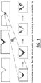
- Fig. 1 shows the fabrication scheme for an oxide pyramid supporting a nanosubstruture metal tip. Fabrication started with the mold fabrication, in this case by KOH etching in a ⁇ 100> silicon wafer to create the pyramidal hole bounded by the ⁇ 111> planes. Next, silicon nitride (220 nm) was deposited by LPCVD (conformal deposition) and isotropically removed in 50% HF (84 min. at room temperature).
- This is a timed etch step which required a 1.23 times over-etching to remove the silicon nitride in the four oblique ribs of the pyramidal hole (a 109.4°) and leaving only a small piece of silicon nitride at the tip.
- a dummy wafer containing the same thickness of silicon nitride was etched in parallel.
- the silicon oxide structural material for the pyramid was formed by local oxidation of the silicon (LOCOS) (see J.A. Appels, E. Kooi, M.M. Paffen, J.J. H. Schatorje, W. Verkuylen, "Local oxidation of silicon and its applications in semiconductor-device technology", Philips Res.
- LOC local oxidation of the silicon
- TMAH is a suitable etchant for this step as it has a high selectivity for silicon as compared to silicon oxide (table 1) [7].
- Fig. 2 shows the fabricated silicon oxide pyramid having a Chromium tip of less than 300 nm in size.
- the pyramid may have particular uses. With wires made of piezoresistive material, such as p++ silicon nano-dot or line, the pyramid may be used for measuring (contact) forces. With wires made material having a temperature dependent electrical resistance, a pyramid may be used for local temperature measurement. Wire dissipating electrical power may be used for local heating.
- the aim of this example is to create a pyramid with tunable nanosubstructure apertures close to the tip.
- Fabrication started with KOH etching of the pyramidal mold in a ⁇ 100> silicon wafer.
- 500 nm LPCVD silicon nitride structural material was conformally deposited, followed by 330 nm LPCVD polysilicon. This layer acted as etching mask in later steps.
- a second layer of silicon nitride (120 nm) was deposited and isotropically etched in 50 %HF in order to remove all of the silicon nitride but a small remnant at the tip ( fig. 3a ).
- This remnant was used as an inversion mask in the LOCOS step (wet oxidation at 900°C for 10 min.) of the polysilicon ( fig. 3b ).
- a timed etching of the polysilicon followed, which starts at the apex of the pyramid and moves up along its sides ( fig. 3c ).
- the duration of this step determines the height of the nano apertures to be formed.
- a confined layer of 330 nm polysilicon etches laterally at a speed of 4.2 ⁇ 10 2 nm/min. in the 5 wt% TMAH solution supplied through a silicon oxide pinhole of sub 100 nm.
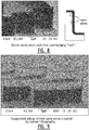
- Fig. 4 shows a typical fabrication result with apertures in the order of 1 ⁇ m in size. The size and the location of the apertures can be tuned by the thickness of in particular the silicon nitride layers and by the polysilicon etching time.
- Example 3 nano fencing: suspended nanowires
- a silicon oxide mold was made containing the appropriate sharp concave corners. Illustrated is the process which was followed by a structure having four vertical wires created in the corners of a square mold.
- a square silicon pillar is etched by deep reactive ion etching (DRIE) with photoresist as the mask material.
- the resist is stripped and the wafer oxidized (wet oxidation at 950 °C) to form the silicon oxide mold (thickness of about 400 nm), fig. 5a .
- DRIE deep reactive ion etching
- an overhanging "roof" is added to the mold to create a horizontally oriented concave corner.
- the fabrication of the mold is illustrated in fig. 7 .
- a silicon pillar is etched by DRIE (Bosch process) using a silicon oxide and silicon nitride bilayer as the mask.
- the silicon oxide is etched in BHF, under-cutting the silicon nitride thin film.
- the silicon nitride is thinned down in hot H 3 PO 4 until it is only left on top of the silicon oxide. Using the remaining mask material a LOCOS step is performed.
- Fig. 8 shows a SEM picture of a typical mold structure. The cross section next to it shows the location of the horizontal nanowires in the concave corners of the mold.
- Fig. 9 shows the resulting suspended nano wire structure formed after conformal deposition of silicon nitride (350 nm by LPCVD), subsequent isotropic thinning of this layer in hot H 3 PO 4 for 83 min., and removal of the mold in BHF .
- Example 4 Method for making a silicon nitride (SiN) pyramid fountain-pen with tunable nano-apertures.
- example 2 is first produced a SiN pyramid with tunable nano-apertures. Subsequently, by further two conformal depositions of structural materials and by sacrificial etching of the formerly deposited structural layer are formed channels for liquid or gas. Finally after removal of the silicon mold, a free hanging inverted pyramid remains containing a fluid/gas supply channel with nano-apertures.
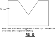
- Figure 10 Mold fabrication: inverted pyramid in mono crystalline silicon created by anisotropic wet etching.
- Figure 11 shows the conformal deposition of 3 layers: LPCVD SiN, LPCVD Poly-Si, LPCVD SiN.
- Figure 12 shows the isotropic removal of the last deposited LPCVD SiN layer.
- Figure 13 shows the 1.23 times over-etching to remove the LPCVD SiN in the four oblique ribs of the inverted pyramid.
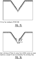
- Figure 14 shows the partly oxidation of the LPCVD poly-Si using the residual LPCVD SiN as inversion mask. (local oxidation of LPCVD poly-Si: LOCOS).
- Figure 15 shows the stripping of the residual LPCVD SiN.
- Figures 16 show the wet etching of poly-Si using the LOCOS-oxide as mask material. Length A can be tuned by the etching time.
- Figure 17 shows the stripping of the LOCOS oxide.
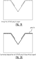
- Figure 18 shows the isotropic etching of the first deposited LPCVD SiN layer using the polysilicon as the etch mask.
- Figure 19 shows the stripping of the poly-silicon layer.
- Figure 20 shows the conformal deposition of LPCVD poly Si (sacrificial layer).
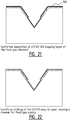
- Figure 21 shows the conformal deposition of LPCVD SiN (capping layer of the fluid/gas channel).
- Figure 22 shows the sacrificial etching of the LPCVD poly-Si layer, leaving a channel for fluid/gas supply.
- Figure 23 shows the removal of the silicon mold, leaving a free hanging inverted pyramid containing a fluid/gas supply channel with nano-apertures.
- Figure 24 is the top drawing represents the top view of the final structure: a SiN pyramid fountain pen with tunable nano-apertures.
- Cross section 1-1 represents figure 23 . Views 2) and 3) show different cross sections.
- the advantage of the fountain pen approach compared with NADIS is that a wider variety of inks can be used (also more volatile ones) and that eventually complex fluidic delivery systems can be made.
- some of the possible advantages of the fountain pen technology are: a larger amount of ink is available, the dependence of the writing process on relative humidity could be less, inks can be mixed at the tip, inks can possibly be changed during writing and electrochemical deposition of for example metals is possible.
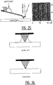
- a cross-section of the prior art probe is shown in figure 25 below, together with a written line pattern of a self-assembled monolayer (ODT) on gold. As can be seen in fig. 25 , the written feature size is still in the order of 1 ⁇ m.
- the final aim in the scope of this proposal is a ten-fold reduction of the line width, so typically sub-100 nm resolution.
- the applicant has ongoing collaborations with the Biophysical Engineering Group of prof. Subramaniam and the Molecular Nanofabrication group of prof. Huskens (both at the university of Twente) on the application of the nanofountain pen, therefore knowledge of different inks and substrates to be tested is available to the project.
Landscapes
- Engineering & Computer Science (AREA)
- Chemical & Material Sciences (AREA)
- Manufacturing & Machinery (AREA)
- Radiology & Medical Imaging (AREA)
- Physics & Mathematics (AREA)
- Health & Medical Sciences (AREA)
- General Health & Medical Sciences (AREA)
- General Physics & Mathematics (AREA)
- Nuclear Medicine, Radiotherapy & Molecular Imaging (AREA)
- Analytical Chemistry (AREA)
- Microelectronics & Electronic Packaging (AREA)
- Nanotechnology (AREA)
- Crystallography & Structural Chemistry (AREA)
- Micromachines (AREA)
- Crystals, And After-Treatments Of Crystals (AREA)
- Semiconductor Memories (AREA)
- Moulds For Moulding Plastics Or The Like (AREA)
- Mounting, Exchange, And Manufacturing Of Dies (AREA)
- Cold Cathode And The Manufacture (AREA)
Applications Claiming Priority (3)
| Application Number | Priority Date | Filing Date | Title |
|---|---|---|---|
| EP08000094A EP2077249A1 (de) | 2008-01-06 | 2008-01-06 | Verfahren zur Herstellung einer 3D-Nanostruktur mit einer Nanounterstruktur und Isolierpyramide mit einer Metallspitze, sowie mit diesem Verfahren herstellbare Pyramide mit Nanoöffnungen und horizontalen und/oder vertikalen Nanodrähten |
| EP08869344.5A EP2231507B1 (de) | 2008-01-06 | 2008-12-22 | Verfahren zur herstellung einer 3d-nanostruktur mit einer nanosubstruktur, wie eine isolierpyramide mit einer metallspitze |
| PCT/EP2008/011107 WO2009086915A1 (en) | 2008-01-06 | 2008-12-22 | A method for making a 3d nanostructure having a nanosubstructure, and an insulating pyramid having a metallic tip, a pyramid having nano-apertures and horizontal and/or vertical nanowires obtainable by this method |
Related Parent Applications (1)
| Application Number | Title | Priority Date | Filing Date |
|---|---|---|---|
| EP08869344.5A Division EP2231507B1 (de) | 2008-01-06 | 2008-12-22 | Verfahren zur herstellung einer 3d-nanostruktur mit einer nanosubstruktur, wie eine isolierpyramide mit einer metallspitze |
Publications (2)
| Publication Number | Publication Date |
|---|---|
| EP3549906A2 true EP3549906A2 (de) | 2019-10-09 |
| EP3549906A3 EP3549906A3 (de) | 2019-12-11 |
Family
ID=39408658
Family Applications (3)
| Application Number | Title | Priority Date | Filing Date |
|---|---|---|---|
| EP08000094A Withdrawn EP2077249A1 (de) | 2008-01-06 | 2008-01-06 | Verfahren zur Herstellung einer 3D-Nanostruktur mit einer Nanounterstruktur und Isolierpyramide mit einer Metallspitze, sowie mit diesem Verfahren herstellbare Pyramide mit Nanoöffnungen und horizontalen und/oder vertikalen Nanodrähten |
| EP08869344.5A Active EP2231507B1 (de) | 2008-01-06 | 2008-12-22 | Verfahren zur herstellung einer 3d-nanostruktur mit einer nanosubstruktur, wie eine isolierpyramide mit einer metallspitze |
| EP19171039.1A Pending EP3549906A3 (de) | 2008-01-06 | 2008-12-22 | Verfahren zur herstellung einer 3d-nanostruktur mit einer nanosubstruktur, wie eine isolierpyramide mit einer metallspitze |
Family Applications Before (2)
| Application Number | Title | Priority Date | Filing Date |
|---|---|---|---|
| EP08000094A Withdrawn EP2077249A1 (de) | 2008-01-06 | 2008-01-06 | Verfahren zur Herstellung einer 3D-Nanostruktur mit einer Nanounterstruktur und Isolierpyramide mit einer Metallspitze, sowie mit diesem Verfahren herstellbare Pyramide mit Nanoöffnungen und horizontalen und/oder vertikalen Nanodrähten |
| EP08869344.5A Active EP2231507B1 (de) | 2008-01-06 | 2008-12-22 | Verfahren zur herstellung einer 3d-nanostruktur mit einer nanosubstruktur, wie eine isolierpyramide mit einer metallspitze |
Country Status (4)
| Country | Link |
|---|---|
| US (2) | US8932473B2 (de) |
| EP (3) | EP2077249A1 (de) |
| JP (1) | JP5501250B2 (de) |
| WO (1) | WO2009086915A1 (de) |
Families Citing this family (12)
| Publication number | Priority date | Publication date | Assignee | Title |
|---|---|---|---|---|
| EP2077249A1 (de) * | 2008-01-06 | 2009-07-08 | Universiteit Twente | Verfahren zur Herstellung einer 3D-Nanostruktur mit einer Nanounterstruktur und Isolierpyramide mit einer Metallspitze, sowie mit diesem Verfahren herstellbare Pyramide mit Nanoöffnungen und horizontalen und/oder vertikalen Nanodrähten |
| FR2934709B1 (fr) * | 2008-08-01 | 2010-09-10 | Commissariat Energie Atomique | Structure d'echange thermique et dispositif de refroidissement comportant une telle structure. |
| CA2798716A1 (en) | 2011-12-13 | 2013-06-13 | Endochoice Innovation Center Ltd. | Removable tip endoscope |
| WO2014003843A1 (en) * | 2012-06-29 | 2014-01-03 | Regents Of The University Of Minnesota | Method of forming individual metallic microstructures |
| US10605827B2 (en) * | 2015-12-14 | 2020-03-31 | Universidade Federal De Menas Gerais-Ufmg | Metallic device for scanning probe microscopy and method for manufacturing same |
| US10689245B2 (en) | 2018-02-27 | 2020-06-23 | International Business Machines Corporation | Vertically stacked nanofluidic channel array |
| CN108673880A (zh) * | 2018-06-13 | 2018-10-19 | 北京化工大学 | 一种具有榫卯结构的3d打印填充结构及其加工工艺 |
| EP3552806A1 (de) | 2018-04-09 | 2019-10-16 | Nederlandse Organisatie voor toegepast- natuurwetenschappelijk onderzoek TNO | Verfahren und vorrichtung zur herstellung eines objekts mittels generativer fertigung |
| NL2022939B1 (en) * | 2019-04-12 | 2020-10-20 | Smarttip Bv | A method of providing a MEMS device comprising a pyramidal protrusion, and a mold |
| CN112062084A (zh) * | 2020-08-25 | 2020-12-11 | 华南理工大学 | 一种高分辨率的硅基中空悬臂探针及其制备方法 |
| NL2026730B1 (en) * | 2020-10-22 | 2022-06-16 | Cytosurge Ag | A method of manufacturing a MEMS device |
| CN116715186B (zh) * | 2023-03-03 | 2025-09-30 | 浙江大学 | 基于仿生学的纤毛光学流体传感器阵列及流场测试方法 |
Family Cites Families (18)
| Publication number | Priority date | Publication date | Assignee | Title |
|---|---|---|---|---|
| JPH06117849A (ja) * | 1992-10-07 | 1994-04-28 | Advantest Corp | Spm用探針及びその製造方法 |
| JP3226238B2 (ja) * | 1993-03-15 | 2001-11-05 | 株式会社東芝 | 電界放出型冷陰極およびその製造方法 |
| US5584740A (en) * | 1993-03-31 | 1996-12-17 | The United States Of America As Represented By The Secretary Of The Navy | Thin-film edge field emitter device and method of manufacture therefor |
| KR100205051B1 (ko) * | 1995-12-22 | 1999-06-15 | 정선종 | 필드 에미션 디스플레이 소자의 제조방법 |
| US5789272A (en) * | 1996-09-27 | 1998-08-04 | Industrial Technology Research Institute | Low voltage field emission device |
| JP3697034B2 (ja) * | 1997-08-26 | 2005-09-21 | キヤノン株式会社 | 微小開口を有する突起の製造方法、及びそれらによるプローブまたはマルチプローブ |
| JP2000123711A (ja) * | 1998-10-12 | 2000-04-28 | Toshiba Corp | 電界放出型冷陰極及びその製造方法 |
| JP3884887B2 (ja) * | 1999-08-27 | 2007-02-21 | 株式会社ルネサステクノロジ | 描画用探針及びその製作方法 |
| JP2001116678A (ja) * | 1999-10-14 | 2001-04-27 | Canon Inc | 光照射用または光検出用プローブの製造方法、および光照射用または光検出用プローブ |
| GB2383187B (en) * | 2001-09-13 | 2005-06-22 | Microsaic Systems Ltd | Electrode structures |
| US6692145B2 (en) * | 2001-10-31 | 2004-02-17 | Wisconsin Alumni Research Foundation | Micromachined scanning thermal probe method and apparatus |
| CN1599939B (zh) * | 2002-01-15 | 2010-08-11 | 国际商业机器公司 | 形成微观结构的方法 |
| AU2003290510A1 (en) * | 2002-06-26 | 2004-04-19 | Cornell Research Foundation, Inc. | Small scale wires with microelectromechanical devices |
| DE10236149A1 (de) * | 2002-08-05 | 2004-02-26 | Universität Kassel | Verfahren zur Herstellung einer eine schmale Schneide oder Spitze aufweisenden Struktur und mit einer solchen Struktur versehener Biegebalken |
| JP2004239704A (ja) * | 2003-02-05 | 2004-08-26 | Renesas Technology Corp | カンチレバーおよびその製造方法 |
| GB0708695D0 (en) * | 2007-05-04 | 2007-06-13 | Univ Nottingham | Fabrication of nanoparticles |
| EP2077249A1 (de) * | 2008-01-06 | 2009-07-08 | Universiteit Twente | Verfahren zur Herstellung einer 3D-Nanostruktur mit einer Nanounterstruktur und Isolierpyramide mit einer Metallspitze, sowie mit diesem Verfahren herstellbare Pyramide mit Nanoöffnungen und horizontalen und/oder vertikalen Nanodrähten |
| WO2010114887A1 (en) * | 2009-03-31 | 2010-10-07 | Georgia Tech Research Corporation | Metal-assisted chemical etching of substrates |
-
2008
- 2008-01-06 EP EP08000094A patent/EP2077249A1/de not_active Withdrawn
- 2008-12-22 WO PCT/EP2008/011107 patent/WO2009086915A1/en not_active Ceased
- 2008-12-22 JP JP2010541027A patent/JP5501250B2/ja active Active
- 2008-12-22 EP EP08869344.5A patent/EP2231507B1/de active Active
- 2008-12-22 US US12/811,674 patent/US8932473B2/en active Active
- 2008-12-22 EP EP19171039.1A patent/EP3549906A3/de active Pending
-
2014
- 2014-12-15 US US14/570,652 patent/US9416001B2/en active Active
Non-Patent Citations (7)
| Title |
|---|
| A. VOLLKOPF; O. RUDOW; M. MULLER-WIEGAND; G. GEORGIEV; E. OESTERSCHULZE: "Influence of the oxidation temperature on the fabrication process of silicon dioxide aperture tips", APPL. PHYS. A, vol. 76, 2003, pages 923 - 926, XP055315247, DOI: doi:10.1007/s00339-002-1450-4 |
| E. SARAJLIC; E. BERENSCHOT; G. KRIJNEN; M. ELWENSPOEK: "Fabrication of 3D Nanowire Frames by Conventional Micromachining Technology", TRANSDUCERS '05 [DIGEST OFTECHN. PAPERS 13TH INT. CONF. ON SOLID-STATE SENSORS, ACTUATORS AND MICROSYSTEMS], pages 27 - 29 |
| J. HANEVELD; E. BERENSCHOT; P. MAURY; H. JANSEN: "Nano-ridge fabrication by local oxidation of silicon edges with silicon nitride as a mask", J. MICROMECH. MICROENG., vol. 16, 2006, pages S24 - S28, XP020105014, DOI: doi:10.1088/0960-1317/16/6/S05 |
| J.A. APPELS; E. KOOI; M.M. PAFFEN; J.J. H. SCHATORJE; W. VERKUYLEN: "Local oxidation of silicon and its applications in semiconductor-device technology", PHILIPS RES. REP., vol. 25, 1970, pages 118 - 132, XP055315252 |
| N.R. TAS; J.W. BERENSCHOT; P. MELA; H.V. JANSEN; M. ELWENSPOEK; A. VAN DEN BERG: "2D-Confined Nanochannels Fabricated by Conventional Micromachining", NANO LETT., vol. 2, 2002, pages 1031 - 1032, XP002283203, DOI: doi:10.1021/nl025693r |
| P.N. MINH; T. ONO; M. ESASHI: "Non-uniform silicon oxidation and application for the fabrication of aperture for near-field scanning optical microscopy", APPL. PHYS. LETT., vol. 75, 1999, pages 4076 - 4078 |
| R.B. MARCUS; T.T. SHENG: "The oxidation of shaped silicon surfaces", J. ELECTROCHEM. SOC., vol. 129, 1982, pages 1278 - 1282, XP000840596 |
Also Published As
| Publication number | Publication date |
|---|---|
| US9416001B2 (en) | 2016-08-16 |
| JP2011511270A (ja) | 2011-04-07 |
| US20150158724A1 (en) | 2015-06-11 |
| JP5501250B2 (ja) | 2014-05-21 |
| EP2231507A1 (de) | 2010-09-29 |
| US20110039100A1 (en) | 2011-02-17 |
| WO2009086915A1 (en) | 2009-07-16 |
| US8932473B2 (en) | 2015-01-13 |
| EP2077249A1 (de) | 2009-07-08 |
| EP2231507B1 (de) | 2019-05-01 |
| EP3549906A3 (de) | 2019-12-11 |
Similar Documents
| Publication | Publication Date | Title |
|---|---|---|
| EP2231507B1 (de) | Verfahren zur herstellung einer 3d-nanostruktur mit einer nanosubstruktur, wie eine isolierpyramide mit einer metallspitze | |
| Ziaie et al. | Introduction to micro-/nanofabrication | |
| US20100081278A1 (en) | Methods for Nanoscale Feature Imprint Molding | |
| US8828243B2 (en) | Scanning probe having integrated silicon tip with cantilever | |
| Rius et al. | Introduction to micro-/nanofabrication | |
| CN102205943A (zh) | 一种单晶硅纳米结构的制备方法 | |
| Zhao et al. | Sub-10 nm silicon ridge nanofabrication by advanced edge lithography for NIL applications | |
| Westerik et al. | Sidewall patterning—a new wafer-scale method for accurate patterning of vertical silicon structures | |
| JP2003302328A (ja) | Spmセンサーおよびその製造法 | |
| US6887395B2 (en) | Method of forming sub-micron-size structures over a substrate | |
| Berenschot et al. | 3D-nanomachining using corner lithography | |
| Sarajlic et al. | Fabrication of 3D nanowire frames by conventional micromachining technology | |
| Mihalcea et al. | Reproducible large‐area microfabrication of sub‐100 nm apertures on hollow tips | |
| Boisen et al. | Indirect tip fabrication for scanning probe microscopy | |
| NL2026730B1 (en) | A method of manufacturing a MEMS device | |
| Berenschot et al. | A method for making a 3D nanostructure having a nanosubstructure, and an insulating pyramid having a metallic tip, a pyramid having nano-apertures and horizontal and/or vertical nanovires obtainable by this method | |
| Haneveld et al. | Nano-ridge fabrication by local oxidation of silicon edges with silicon nitride as a mask | |
| Golod et al. | Directional-rolling method for strained SiGe/Si films and its application to fabrication of hollow needles | |
| JP2005535137A (ja) | 基板上の層に少なくとも1つの小開口を作るための方法およびかかる方法で製造されたコンポーネントパーツ | |
| US11035880B2 (en) | Method for producing a probe suitable for scanning probe microscopy | |
| Berenschot et al. | Wafer-scale nanostructure formation inside vertical nano-pores | |
| EP3953716B1 (de) | Herstellungsverfahren einer mems-vorrichtung, eine spitze enthaltende, und formkörper | |
| Xie et al. | Fabrication of localized plasma gold-tip nanoprobes with integrated microchannels for direct-write nanomanufacturing | |
| Lin et al. | A liquid-based gravity-driven etching-stop technique and its application to wafer level cantilever thickness control of AFM probes | |
| Yifang et al. | Fabrication of nano-tips employing three different methods |
Legal Events
| Date | Code | Title | Description |
|---|---|---|---|
| PUAI | Public reference made under article 153(3) epc to a published international application that has entered the european phase |
Free format text: ORIGINAL CODE: 0009012 |
|
| STAA | Information on the status of an ep patent application or granted ep patent |
Free format text: STATUS: THE APPLICATION HAS BEEN PUBLISHED |
|
| AC | Divisional application: reference to earlier application |
Ref document number: 2231507 Country of ref document: EP Kind code of ref document: P |
|
| AK | Designated contracting states |
Kind code of ref document: A2 Designated state(s): AT BE BG CH CY CZ DE DK EE ES FI FR GB GR HR HU IE IS IT LI LT LU LV MC MT NL NO PL PT RO SE SI SK TR |
|
| AX | Request for extension of the european patent |
Extension state: AL BA MK RS |
|
| PUAL | Search report despatched |
Free format text: ORIGINAL CODE: 0009013 |
|
| AK | Designated contracting states |
Kind code of ref document: A3 Designated state(s): AT BE BG CH CY CZ DE DK EE ES FI FR GB GR HR HU IE IS IT LI LT LU LV MC MT NL NO PL PT RO SE SI SK TR |
|
| AX | Request for extension of the european patent |
Extension state: AL BA MK RS |
|
| RIC1 | Information provided on ipc code assigned before grant |
Ipc: G01Q 70/16 20100101ALI20191107BHEP Ipc: B81C 1/00 20060101AFI20191107BHEP Ipc: G01Q 70/10 20100101ALI20191107BHEP |
|
| RIC1 | Information provided on ipc code assigned before grant |
Ipc: G01Q 70/10 20100101ALI20191114BHEP Ipc: B81C 1/00 20060101AFI20191114BHEP Ipc: G01Q 70/16 20100101ALI20191114BHEP |
|
| STAA | Information on the status of an ep patent application or granted ep patent |
Free format text: STATUS: REQUEST FOR EXAMINATION WAS MADE |
|
| 17P | Request for examination filed |
Effective date: 20200604 |
|
| RBV | Designated contracting states (corrected) |
Designated state(s): AT BE BG CH CY CZ DE DK EE ES FI FR GB GR HR HU IE IS IT LI LT LU LV MC MT NL NO PL PT RO SE SI SK TR |
|
| STAA | Information on the status of an ep patent application or granted ep patent |
Free format text: STATUS: EXAMINATION IS IN PROGRESS |
|
| 17Q | First examination report despatched |
Effective date: 20220303 |