EP3550330B1 - Dispositif de mesure de distance - Google Patents
Dispositif de mesure de distance Download PDFInfo
- Publication number
- EP3550330B1 EP3550330B1 EP17876971.7A EP17876971A EP3550330B1 EP 3550330 B1 EP3550330 B1 EP 3550330B1 EP 17876971 A EP17876971 A EP 17876971A EP 3550330 B1 EP3550330 B1 EP 3550330B1
- Authority
- EP
- European Patent Office
- Prior art keywords
- pixel
- exposure
- light
- image sensor
- solid
- Prior art date
- Legal status (The legal status is an assumption and is not a legal conclusion. Google has not performed a legal analysis and makes no representation as to the accuracy of the status listed.)
- Active
Links
Images




Classifications
-
- G—PHYSICS
- G01—MEASURING; TESTING
- G01S—RADIO DIRECTION-FINDING; RADIO NAVIGATION; DETERMINING DISTANCE OR VELOCITY BY USE OF RADIO WAVES; LOCATING OR PRESENCE-DETECTING BY USE OF THE REFLECTION OR RERADIATION OF RADIO WAVES; ANALOGOUS ARRANGEMENTS USING OTHER WAVES
- G01S17/00—Systems using the reflection or reradiation of electromagnetic waves other than radio waves, e.g. lidar systems
- G01S17/02—Systems using the reflection of electromagnetic waves other than radio waves
- G01S17/06—Systems determining position data of a target
- G01S17/08—Systems determining position data of a target for measuring distance only
- G01S17/10—Systems determining position data of a target for measuring distance only using transmission of interrupted, pulse-modulated waves
-
- G—PHYSICS
- G01—MEASURING; TESTING
- G01S—RADIO DIRECTION-FINDING; RADIO NAVIGATION; DETERMINING DISTANCE OR VELOCITY BY USE OF RADIO WAVES; LOCATING OR PRESENCE-DETECTING BY USE OF THE REFLECTION OR RERADIATION OF RADIO WAVES; ANALOGOUS ARRANGEMENTS USING OTHER WAVES
- G01S7/00—Details of systems according to groups G01S13/00, G01S15/00, G01S17/00
- G01S7/48—Details of systems according to groups G01S13/00, G01S15/00, G01S17/00 of systems according to group G01S17/00
- G01S7/483—Details of pulse systems
- G01S7/486—Receivers
- G01S7/4861—Circuits for detection, sampling, integration or read-out
- G01S7/4863—Detector arrays, e.g. charge-transfer gates
-
- G—PHYSICS
- G01—MEASURING; TESTING
- G01C—MEASURING DISTANCES, LEVELS OR BEARINGS; SURVEYING; NAVIGATION; GYROSCOPIC INSTRUMENTS; PHOTOGRAMMETRY OR VIDEOGRAMMETRY
- G01C3/00—Measuring distances in line of sight; Optical rangefinders
- G01C3/02—Details
- G01C3/06—Use of electric means to obtain final indication
-
- G—PHYSICS
- G01—MEASURING; TESTING
- G01S—RADIO DIRECTION-FINDING; RADIO NAVIGATION; DETERMINING DISTANCE OR VELOCITY BY USE OF RADIO WAVES; LOCATING OR PRESENCE-DETECTING BY USE OF THE REFLECTION OR RERADIATION OF RADIO WAVES; ANALOGOUS ARRANGEMENTS USING OTHER WAVES
- G01S17/00—Systems using the reflection or reradiation of electromagnetic waves other than radio waves, e.g. lidar systems
- G01S17/88—Lidar systems specially adapted for specific applications
- G01S17/89—Lidar systems specially adapted for specific applications for mapping or imaging
-
- G—PHYSICS
- G01—MEASURING; TESTING
- G01S—RADIO DIRECTION-FINDING; RADIO NAVIGATION; DETERMINING DISTANCE OR VELOCITY BY USE OF RADIO WAVES; LOCATING OR PRESENCE-DETECTING BY USE OF THE REFLECTION OR RERADIATION OF RADIO WAVES; ANALOGOUS ARRANGEMENTS USING OTHER WAVES
- G01S17/00—Systems using the reflection or reradiation of electromagnetic waves other than radio waves, e.g. lidar systems
- G01S17/88—Lidar systems specially adapted for specific applications
- G01S17/89—Lidar systems specially adapted for specific applications for mapping or imaging
- G01S17/894—Three-dimensional [3D] imaging with simultaneous measurement of time-of-flight at a two-dimensional [2D] array of receiver pixels, e.g. time-of-flight cameras or flash lidar
-
- G—PHYSICS
- G01—MEASURING; TESTING
- G01S—RADIO DIRECTION-FINDING; RADIO NAVIGATION; DETERMINING DISTANCE OR VELOCITY BY USE OF RADIO WAVES; LOCATING OR PRESENCE-DETECTING BY USE OF THE REFLECTION OR RERADIATION OF RADIO WAVES; ANALOGOUS ARRANGEMENTS USING OTHER WAVES
- G01S7/00—Details of systems according to groups G01S13/00, G01S15/00, G01S17/00
- G01S7/48—Details of systems according to groups G01S13/00, G01S15/00, G01S17/00 of systems according to group G01S17/00
- G01S7/483—Details of pulse systems
- G01S7/486—Receivers
- G01S7/4868—Controlling received signal intensity or exposure of sensor
-
- G—PHYSICS
- G01—MEASURING; TESTING
- G01S—RADIO DIRECTION-FINDING; RADIO NAVIGATION; DETERMINING DISTANCE OR VELOCITY BY USE OF RADIO WAVES; LOCATING OR PRESENCE-DETECTING BY USE OF THE REFLECTION OR RERADIATION OF RADIO WAVES; ANALOGOUS ARRANGEMENTS USING OTHER WAVES
- G01S7/00—Details of systems according to groups G01S13/00, G01S15/00, G01S17/00
- G01S7/48—Details of systems according to groups G01S13/00, G01S15/00, G01S17/00 of systems according to group G01S17/00
- G01S7/491—Details of non-pulse systems
- G01S7/4912—Receivers
- G01S7/4915—Time delay measurement, e.g. operational details for pixel components; Phase measurement
-
- G—PHYSICS
- G02—OPTICS
- G02B—OPTICAL ELEMENTS, SYSTEMS OR APPARATUS
- G02B7/00—Mountings, adjusting means, or light-tight connections, for optical elements
- G02B7/28—Systems for automatic generation of focusing signals
- G02B7/30—Systems for automatic generation of focusing signals using parallactic triangle with a base line
- G02B7/32—Systems for automatic generation of focusing signals using parallactic triangle with a base line using active means, e.g. light emitter
Definitions
- the present disclosure relates to distance measuring devices that generate a distance image, and in particular to a distance measuring device that includes a radiation light source and a solid-state image sensor that receives light, and measures a distance using delay in the round trip of light.
- TOF time of flight
- distance measurement is performed by causing a solid-state image sensor including a pixel array to receive light reflected by a subject, and generating the amount of signal as a distance image indicating a distance distribution on a two-dimensional plane (see, for example, Patent Literatures 1 to 3).
- NPL 1 NAYAR S K et al: "High Dynamic Range Imaging : Spatially Varying Pixel Exposures", PROCEEDINGS 2000 IEEE CONFERENCE ON COMPUTER VISION AND PATTERN RECOGNITION. CVPR 2000. HILTON HEAD ISLAND, SC, JUNE 13-15, 2000; LOS ALAMITOS, CA: 1EEE COMP., 13 JUNE 2000 (2000-06-13), PAGES 472-479, XP002236923, ISBN: 978-0-7803-6527-8
- conventional distance measuring devices obtain a distance image under an exposure condition that differs for each time series on a per frame basis, devices having a narrow distance measurable range have the accuracy of distance measurement that decreases when a distance to an object changes.
- the conventional distance measuring devices measure a distance by combining distance images that differ in exposure, the conventional distance measuring devices have unstable measurement accuracy due to a variation in the exposures resulting in the distance images when the distance images include ambient light other than radiation light, such as background light.
- the present disclosure has an object to provide a distance measuring device that can perform distance measurement with reasonable accuracy in a distance measurement range that is unaffected by the distance change of an object.
- a distance measuring device of the present disclosure is a distance measuring device that measures a distance to an object using a round-trip time distance images include ambient light other than radiation light, such as background light.
- the present disclosure has an object to provide a distance measuring device that can perform distance measurement with reasonable accuracy in a distance measurement range that is unaffected by the distance change of an object.
- a distance measuring device of the present disclosure is a distance measuring device that measures a distance to an object using a round-trip time of light, and includes: a light emitter including a light source that radiates light to a measurement target range; a solid-state image sensor that includes a plurality of pixels included in a plurality of pixel groups capable of being exposed independently, and causes the plurality of pixels to perform photoelectric conversion of reflected light from the object within an angle of view of radiation light from the light emitter, the plurality of pixels being arranged in a matrix; a light emission and exposure controller that (i) instructs a light emission timing and a light emission period of the light source to the light emitter, (ii) instructs, to each of the plurality of pixel groups in the solid-state image sensor, an exposure timing and an exposure period for obtaining pixel signals of types corresponding to a time difference between the radiation light and the reflected light due to a round-trip time of light, and the light emission and exposure controller further (iii) intermittently exposes the pluralit
- a distance measuring device can perform distance measurement with reasonable accuracy in a distance measurement range that is unaffected by the distance change of an object.
- Devices for or methods of generating an image (hereinafter also referred to as a distance image) having the distance information of a subject have been recently applied not only to the gaming or amusement field but also to a field in which a two-dimensional image sensor, such as a vehicle-mounted camera or a security camera, are used.
- a two-dimensional image sensor such as a vehicle-mounted camera or a security camera
- Examples of a method of measuring a distance to a subject to generate a distance image include a method of generating a distance image based on a parallax between images captured by cameras, and a method of generating a distance image based on a parallax resulting from radiating light having a known random dot pattern to a subject and receiving reflected light having the dot pattern.
- a distance to a subject is calculated (measured) based on a measurement time from when infrared light or laser light is radiated to the subject to when light reflected by the subject is received by a solid-state image sensor.
- a solid-state image sensor including a pixel array is caused to receive light reflected by a subject, distance information can be obtained, for each pixel of the solid-state image sensor, from the obtained amount of signal, and a distance image indicating a distance distribution on a two-dimensional plane can be obtained.
- the intensity of received reflected light changes greatly according to a distance from the solid-state image sensor to the subject or the surface reflectance of the subject.
- the intensity of a radiation light source, the light sensitivity of the solid-state image sensor, or an exposure amount is kept constant.
- the intensity of reflected light received by the solid-state image sensor depends on the characteristics of light that attenuates in inverse proportion to a square of the distance from the light source to the subject, or the surface reflectance of the subject. For example, when an exposure amount is increased by adjusting exposure to reflected light, the intensity of reflected light from a close subject or a subject having a high surface reflectance becomes higher, and the exposure amount exceeds an exposure amount receivable by the solid-state image sensor to reach a saturation state. In this case, it is impossible to obtain a correct light amount signal. Conversely, when an exposure amount is decreased, the amount of reflected light from a far subject or a subject having a low surface reflectance becomes very small. In this case, it is difficult to stably measure a distance.
- PTLs 1, 2, and 3 are disclosed as solutions to such a technical problem as described above.
- signal charge storage times are separately set for even-numbered pixel rows and odd-numbered pixel rows to extract signals having different sensitivities, and a signal-processing system disposed at a subsequent stage combines the signals having the different sensitivities.
- a storage time is set to be long for each pixel of the even-numbered rows to obtain a pixel signal having a high sensitivity
- a storage time is set to be short for each pixel of the odd-numbered rows to obtain a pixel signal having a low sensitivity.
- pixel signals (pixel signals having a high sensitivity) in the even-numbered rows are selected from pixels in the even-numbered rows when the pixel signals in the even-numbered rows are not saturated
- pixel signals (pixel signals having a low sensitivity) in the odd-numbered rows are selected from adjacent pixels in the odd-numbered rows when the pixel signals in the even-numbered rows are saturated.
- the distance measuring device since a distance measuring device in PTL 1 or 3 obtains a distance image under an exposure condition that differs for each time series on a per frame basis, the distance measuring device has the accuracy of distance measurement that decreases when a distance to an object changes. Moreover, since the distance measuring device stores distance images that differ in exposure, the distance measuring device requires a frame memory that stores a distance value for each pixel of a solid-state image sensor. For this reason, the increase in the number of pixels of the solid-state image sensor requires a larger-capacity frame memory, and the distance measuring device grows in size and costs higher.
- a distance measuring device to be described below can expand the distance measurement range of a solid-state image sensor within one frame, and obtain a distance image that is unaffected when a distance to an object changes along time series, the distance measurement range being restricted by the attenuation of light caused by the distance to the object or a decrease in the intensity of reflected light caused by the surface reflectance of the object. Moreover, the distance measuring device can remove the influence of disturbance caused by background light other than radiation light, and obtain a distance image having reasonable accuracy. For this reason, it is possible to provide the distance measuring device that does not require a frame memory or the like, is small, and costs low.
- Each of the following embodiments describes, as an example, a case in which a TOF technique is used for measuring a distance by radiating light-emitting diode (LED) light or laser light to a subject and calculating a round-trip time of reflected light from the subject.
- LED light-emitting diode
- FIG. 1 is a schematic block diagram illustrating distance measuring device 100 according to Embodiment 1 or 2.
- Distance measuring device 100 shown in FIG. 1 includes light emission and exposure controller 101, solid-state image sensor 102, signal processor 103, and light emitter 104.
- solid-state image sensor 102 examples include a charge-coupled device (CCD) image sensor and a complementary metal-oxide-semiconductor image (CMOS) sensor.
- CCD charge-coupled device
- CMOS complementary metal-oxide-semiconductor image
- Light emitter 104 includes light source driver 114 and light source 115.
- Examples of light source 115 include an LED and a laser diode.
- Signal processor 103 includes line memory 111, combiner 112, and distance calculator 113.
- Light emission and exposure controller 101 generates and outputs light emission timing signal LT1, exposure timing signal ET1, and shutter timing signal SH1 according to a predetermined condition to be described below.
- ON and OFF control is performed on light source driver 114 in light emitter 104 according to light emission timing signal LT1, and light source 115 radiates light L1 toward object OBJ.
- Radiation light L1 is pulsed light having a predetermined light emission width.
- Solid-state image sensor 102 includes pixels arranged in a matrix. Solid-state image sensor 102 controls the exposure of each pixel according to exposure timing signal ET1 and shutter timing signal SH1. A pixel signal corresponding to signal charges obtained as a result of photoelectric conversion and accumulated in each pixel is outputted to signal processor 103.
- FIG. 2 is a diagram illustrating an example of the TOF technique.
- the following describes an example of a method of measuring a distance in the TOF technique with reference to FIG. 2 .
- the following are performed in the TOF technique: S0 exposure in which all of reflected light of pulsed light radiated by a light source is received; S1 exposure in which part of reflected light corresponding to a delayed time is received, the reflected light being temporally delayed due to a distance to an object by which the pulsed light is reflected; and BG exposure in which only background light is received without causing the light source to emit light.
- background light is also received simultaneously in S0 exposure and S1 exposure.
- Electric charges are accumulated by repeating these three types of exposure multiple times, and pixel signals S0, S1, and BG corresponding to the amount of electric charges are obtained.
- a light emission pulse width (a radiation pulse time width) is denoted as T 0 and the speed of light is denoted as c
- distance L from the light source to object OBJ can be determined by Expression 1.
- FIG. 3 is a diagram illustrating another example of the TOF technique.
- the length of an exposure period of the solid-state image sensor is approximately identical to a light emission pulse width, and there are S0 exposure in which reflected light reflected by an object and returning belatedly is received in approximately the same exposure period as the pulse light emission timing of radiation light, and S1 exposure in which part of reflected light returning after the completion of pulse light emission of radiation light is received.
- distance L to object OBJ can be determined by Expression 2.
- exposure signal timings and distance calculation expressions are not limited to the above.
- four pixel signals are obtained for each pixel group by emitting radiation light in sine waveform and receiving reflected light at timings corresponding to a phase of 0 degree, a phase of 90 degrees, a phase of 180 degrees, and a phase of 270 degrees relative to a phase of the sine wave of the radiation light.
- Pixel signal groups (S0, S1, BG) inputted to signal processor 103 are stored corresponding to the pixels of solid-state image sensor 102 on a per line basis, in line memory 111.
- Combiner 112 obtains necessary pixel signals of reference pixels from line memory 111, and performs a combination process on the pixel signals.
- the result of the combination process performed by combiner 112 is inputted to distance calculator 113, and distance calculator 113 performs the calculation of Expression 1 or 2 using the combined pixel signals, and outputs distance value DO obtained as the result of the calculation.
- exposure timing signal ET1 outputted from light emission and exposure controller 101 includes a group of signals ET10a, ET11a, and ET12a and a group of signals ET10b, ET11b, and ET12b, each of the groups including a group of three exposure signals that are specifically exposure signal S0, exposure signal S1, and exposure signal BG described above.
- Light emission and exposure controller 101 outputs the signal groups to solid-state image sensor 102.
- FIG. 4 is a schematic diagram illustrating a solid-state image sensor in a distance measuring device according to the present embodiment.
- FIG. 4 shows an example of a connection relationship between the pixel cells of solid-state image sensor 102 and exposure timing signal lines.
- P01, P02, P03, ... in FIG. 4 denote the pixel cells each including a photodiode region.
- the pixel cells are displaced from their pixel positions by a half-pixel pitch in the horizontal direction between the odd-numbered lines and the even-numbered lines on a per line basis.
- Three signal lines for exposure timing signals ET10a, ET11a, and ET12a are connected to the pixel cells in the odd-numbered lines, and three signal lines for exposure timing signals ET10b, ET11b, and ET12b are connected to the pixel cells in the even-numbered lines.
- a line for supplying shutter timing signal SH1 is connected to all the pixel cells.
- FIG. 5 is a schematic diagram illustrating, as an example, a pixel cell of the solid-state image sensor in the distance measuring device according to the present embodiment.
- Photodiode 501 that performs photoelectric conversion is connected to reset transistor 502, and electric charges obtained as a result of photoelectric conversion by photodiode 501 are discarded when shutter timing signal SH1 becomes ON.
- photodiode 501 is connected to analog memories 520, 521, and 522 via analog switches 510, 511, and 512.
- exposure timing signal ET10a is supplied for ON and OFF control of analog switch 510
- exposure timing signal ET11a is supplied for ON and OFF control of analog switch 511
- exposure timing signal ET12a is supplied for ON and OFF control of analog switch 512.
- exposure timing signal ET10b is supplied for ON and OFF control of analog switch 510
- exposure timing signal ET11b is supplied for ON and OFF control of analog switch 511
- exposure timing signal ET12b is supplied for ON and OFF control of analog switch 512.
- Analog memories 520, 521, and 522 accumulate electric charges obtained as a result of photoelectric conversion by photodiode 501, during a period in which analog switches 510, 511, and 512 connected to analog memories 520, 521, and 522 are ON, and a non-reset period in which reset transistor 502 is OFF. Further, analog memories 520, 521, and 522 do not accumulate electric charges during a period in which analog switches 510, 511, and 512 connected to analog memories 520, 521, and 522 are ON and a period in which reset transistor 502 is ON, or during a period in which analog switches 510, 511, and 512 are OFF.
- solid-state image sensor 102 can perform exposure control on each odd-numbered line and each even-numbered line independently.
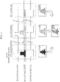
- FIG. 6A and FIG. 6B each show, as the first example of light emission and exposure control, an example of a relationship among an exposure timing signal, radiation light, and shutter timing signal SH1 outputted by light emission and exposure controller 101.
- FIG. 6A is a timing chart for light emission and exposure control in the distance measuring device according to the present embodiment.
- pulsed radiation light emitted according to light emission timing signal LT1 generated and outputted by light emission and exposure controller 101, and exposure timing signal ET1 and shutter timing signal SH1 generated and outputted by light emission and exposure controller 101 are repeatedly outputted in cycles each of which has the same pattern.
- a time of one cycle (cycle Tcyc of an exposure period) is determined by, for example, 1/n (n is an integer greater than or equal to 2) of a light quantity fluctuation cycle (cycle time Tbg of a light source) of illumination light from a lighting device receiving power from a commercial AC source in an environment in which distance measuring device 100 is used.
- FIG. 6B is a diagram obtained by enlarging one cycle period in above-described FIG. 6A .
- One cycle period includes, based on TOF technique 1 shown in above-described FIG. 2 and by Expression 1, an S0 exposure period, an S1 exposure period, and a BG exposure period that are formed according to shutter timing signal SH1 that is outputted by light emission and exposure controller 101 and generates a timing at which reset transistor 502 becomes ON.
- Exposure timing signals ET10a and ET10b are supplied in the S0 exposure period, exposure timing signals ET11a and ET11b are supplied in the S1 exposure period, and exposure timing signals ET12a and ET12b are supplied in the BG exposure period.
- exposure timing signal ET10a is supplied in a period corresponding to 8 pulses of pulsed radiation light emitted according to light emission timing signal LT1
- exposure timing signal ET11b is supplied in a period corresponding to only 2 pulses.
- a time (the first condition) for accumulating, in analog memory 520, signals obtained as a result of photoelectric conversion by each pixel in the odd-numbered lines in solid-state image sensor 102 and a time (the second condition) for accumulating, in analog memory 520, signals obtained as a result of photoelectric conversion by each pixel in the even-numbered lines in solid-state image sensor 102 have a relationship in which the ratio of the signal accumulation times corresponding to exposure times is 4 : 1.
- the present embodiment has described an example of control in which the exposure time ratio is 4 : 1, the present embodiment is not limited to this. It is possible to easily determine a different exposure time ratio by modifying the above-described timing control.
- AOodd denotes the signal component due to radiation light
- B0odd denotes the signal component of background light
- Slodd is expressed by Expression 4.
- S 1 odd A 1 odd + B 1 odd
- Alodd denotes the signal component due to radiation light
- Blodd denotes the signal component of background light
- a signal accumulated in analog memory 521 of the one pixel cell in the odd-numbered line in solid-state image sensor 102 by the BG exposure is denoted as BGodd.
- SOevn A 0 evn + B 0 evn
- AOevn denotes the signal component due to radiation light
- B0evn denotes the signal component of background light
- Alevn denotes the signal component due to radiation light
- Blevn denotes the signal component of background light
- a signal accumulated in analog memory 521 of the other pixel cell in the even-numbered line in solid-state image sensor 102 by the BG exposure is denoted as BGevn.
- the S0 exposure, the S1 exposure, and the BG exposure are performed on the odd-numbered lines and the even-numbered lines in solid-state image sensor 102 to obtain pixel signals in each of six cyclical exposure periods in the present embodiment.
- the cycle of each exposure period is one-third of one cycle of a light quantity fluctuation in illumination light from the lighting device receiving the power from the commercial AC source, and intermittent exposure is performed.
- the operations of light emission and exposure controller 101 in the first example of the light emission and exposure control make it possible to average the signals including the background light components subject to the fluctuation in intensity of the illumination light. For this reason, it is possible to eliminate an unbalanced amount of the signals including the background light components among the S0 exposure, the S1 exposure, and the BG exposure for the odd-numbered lines and the even-numbered lines in solid-state image sensor 102.
- the background light component of a pixel signal is greatly affected by locally biased intensities of fluctuating background light.
- the locally biased intensities of the background light are averaged to make signal S0 and signal S1 identical in background light component to signal BG, it is possible to accurately extract signals including illumination light components in the S0 exposure and the S1 exposure.
- the method of controlling light emission control timing shown in FIG. 7 is different from the method of controlling light emission and exposure timing shown in FIG. 6A .
- the emission of illumination light for exposing odd-numbered lines, which is the first condition is temporally separated from the emission of illumination light for exposing even-numbered lines, which is the second condition.
- solid-state image sensor 102 sequentially reads out signal S0, signal S1, and signal BG for each pixel in the pixel array in the order of raster scan, using a built-in timing generator not shown etc.
- the read signal S0, signal S1, and signal BG for each pixel are outputted to signal processor 103.
- the pixel signals inputted from solid-state image sensor 102 are sequentially stored as signals SOodd, signals Slodd, and signals BGodd of the odd-numbered lines as many as a predetermined number of lines, and signals SOevn, signals S2evn, and signals BGevn of the even-numbered lines as many as a predetermined number of lines, in line memory 111 in signal processor 103.
- the pixel signals to be sequentially referred to are outputted to combiner 112.
- FIG. 8 is a schematic block diagram illustrating the combiner in the distance measuring device according to Embodiment 1.
- combiner 112 includes combination calculation processor 801, first condition background light remover 802, first condition saturation determiner 803, second condition background light remover 804, and second condition saturation determiner 805.
- FIG. 9 is a pixel diagram referred to by combiner 112 in the distance measuring device according to the present embodiment.
- Combiner 112 receives, from line memory 111, signals S0, signals S1, and signals BG of one pixel in the odd-numbered line and four pixels in the even-numbered lines which are adjacent above and below to the one pixel as shown in FIG. 9 , the one pixel and the four pixels being included as processing objects in target pixel group A.
- a pixel group of P01, P02, P11, P21, and P22 in FIG. 9 is target pixel group A.
- Combiner 112 sequentially performs a combination process on, for example, a group of P02, P03, P12, P22, and P23 and a group of P21, P22, P31, P41, and P42.
- P01, P02, P11, P21, and P22, target pixel group A in FIG. 9 are used as an example.
- SOodd (P11), Slodd (P11), and BGodd (P11) of the one pixel in the odd-numbered line are inputted to first condition background light remover 802 and first condition saturation determiner 803.
- SOodd (P11), Slodd (P11), and BGodd (P11) denote signal SOodd, signal Slodd, and signal BGodd of pixel 11, respectively.
- First condition background light remover 802 makes a calculation using Expression 11, and outputs AOodd (P11) and Alodd (P11) to combination calculation processor 801.
- A0odd P11 S0odd P11 ⁇ BGodd P11
- A1odd P11 S1odd P11 ⁇ BGodd P11
- First condition saturation determiner 803 determines the conditions of Expression 12 for saturation determination threshold value Smax pre-set corresponding to the output signal range of solid-state image sensor 102. When any of the conditions of Expression 12 is satisfied, first condition saturation determiner 803 informs combination calculation processor 801 about the presence of a saturation signal. S0odd P11 > Smax S1odd P11 > Smax BGodd P11 > Smax
- Input signals SOevn (P01), Slevn (P01), BGevn (P01), SOevn (P02), Slevn (P02), BGevn (P02), SOevn (P21), Slevn (P21), BGevn (P21), and SOevn (P22), Slevn (P22), BGevn (P22) of the four pixels in the even-numbered lines are inputted to second condition background light remover 804 and second condition saturation determiner 805.
- Second condition background light remover 804 makes a calculation using Expression 13, and outputs AOevn (P01), Alevn (P01), AOevn (P02), Alevn (P02), AOevn (P21), Alevn (P21), AOevn (P22), and Alevn (P22) to combination calculation processor 801.
- Second condition saturation determiner 805 determines the conditions of Expression 14 for the above-described threshold value Smax. When any of the conditions of Expression 14 is satisfied, second condition saturation determiner 805 informs combination calculation processor 801 about the presence of a saturation signal.
- FIG. 10 is a flowchart illustrating the steps of combination calculation in distance measuring device 100 according to the present embodiment.
- second condition saturation determiner 805 determines whether a saturation signal is present (Step S1001). When the saturation signal is determined to be present (Y in Step S1001), second condition saturation determiner 805 informs combination calculation processor 801 about the presence of the saturation signal. In this case, combination calculation processor 801 performs a distance unmeasurable process (Step S1005).
- combination calculation processor 801 outputs a distance unmeasurable state to distance calculator 113.
- first condition saturation determiner 803 determines whether a saturation signal is present (Step S1002). When the saturation signal is determined to be present (Y in Step S1002), first condition saturation determiner 803 informs combination calculation processor 801 about the presence of the saturation signal. In this case, combination calculation processor 801 performs combination calculation 2 (Step S1004). When the saturation signal is determined to be absent, combination calculation processor 801 performs combination calculation 1 (Step S1003).
- combination calculation processor 801 makes a calculation using Expression 15, and outputs AOmix and Almix to distance calculator 113.
- A0mix A0odd P11 + A0evn P01 + A0evn P02 + A0evn P21 + A0evn P22
- A1mix A1odd P11 + A1evn P01 + A1evn P02 + A1evn P21 + A1evn P22
- FIG. 11A is a graph illustrating a relationship between the amount of signal obtained by combination calculation 1 and an input signal in the distance measuring device according to Embodiment 1.
- combination calculation 1 achieves a high S/N ratio. Accordingly, since a horizontally and vertically symmetrical low-pass filter is formed that has a ratio of 1 : 3 : 3 : 1 at the half cycle of a pixel pitch in the horizontal direction and a ratio of 1 : 2 : 1 at the cycle of a pixel pitch in the vertical direction, there is no imbalance in spatial sampling points.
- combination calculation processor 801 makes a calculation using Expression 16 with only pixel signals obtained under the second condition, and outputs AOmix and Almix to distance calculator 113.
- A0mix A0evn P01 + A0evn P02 + A0evn P21 + A0evn P21 ⁇ K
- A1mix A1evn P01 + A1evn P02 + A1evn P21 + A1evn P22 ⁇ K
- coefficient K in Expression 16 is predetermined from a ratio between the total value of one pixel having an exposure time under the first condition and the total value of four pixels having an exposure time under the second condition.
- K is 2 in the present embodiment as calculated below.
- FIG. 11B is a relationship diagram illustrating a relationship between the amount of signal obtained by combination calculation 2 and an input signal.
- a spatial low-pass filter or bilateral filter is disposed between combiner 112 and distance calculator 113 to further reduce, for example, signal noise by integrating, with a scale, the amount of signal obtained by combination calculation 1 via multiplication of coefficient K, even if reference pixel groups of the spatial filter have saturated and unsaturated pixel signals obtained as a result of exposure under the first condition, it is possible to properly perform filtering because the continuity of the amount of signal is maintained. This concludes the description of the first example of combiner 112.
- FIG. 11B is a graph illustrating a relationship between the amount of signal obtained by combination calculation 2 and an input signal in distance measuring device 100 according to the present embodiment.
- FIG. 12 is a pixel diagram referred to by combiner 112.
- Combiner 112 receives, from line memory 111, signals S0, signals S1, and signals BG of one pixel in the odd-numbered line and one pixel in the even-numbered line which is adjacent above or below to the one pixel as shown in FIG. 12 , the pixels being included as processing objects in target pixel group B.
- the pixel group of P01 and P11 in FIG. 12 is target pixel group B.
- Combiner 112 sequentially performs a signal process on the group of P02 and P11 and the group of P11 and P21.
- P01 and P11, target pixel group B in FIG. 12 are used as an example.
- combiner 112 that performs combination calculation 2 is the same as shown in FIG. 8 .
- Input signals SOodd (P11), Slodd (P11), and BGodd (P11) of the one pixel in the odd-numbered line are inputted to first condition background light remover 802 and first condition saturation determiner 803.
- First condition background light remover 802 makes the same calculation using Expression 11 as described above, and outputs AOodd (P11) and Alodd (P11) to combination calculation processor 801.
- First condition saturation determiner 803 determines the same conditions of Expression 12, and compares above-described pre-set threshold value Smax with SOodd (P11), Slodd (P11), and BGodd (P11). When any of the input signals satisfies a condition of being greater, first condition saturation determiner 803 informs combination calculation processor 801 about the presence of a saturation signal.
- Input signals SOevn (P01), Slevn (P01), and BGevn (P01) of the one pixel in the even-numbered line are inputted to second condition background light remover 804 and second condition saturation determiner 805.
- Second condition background light remover 804 makes a calculation using Expression 17, and outputs AOevn (P01), Alevn (P01), and AOevn (P02) to combination calculation processor 801.
- A0evn P01 S0evn P01 ⁇ BGevn P01
- A1evn P01 S1evn P01 ⁇ BGevn P01
- Second condition saturation determiner 805 determines the conditions of Expression 18 for above-described threshold value Smax. When any of the conditions is satisfied, second condition saturation determiner 805 informs combination calculation processor 802 about the presence of a saturation signal. S0evn P01 > Smax S1evn P01 > Smax BGevn P01 > Smax
- combination calculation processor 801 The procedure of combination calculation processor 801 is the same as shown in FIG. 10 , but how combination calculation 1 and combination calculation 2 are performed is different from FIG. 10 .
- combination calculation processor 801 makes a calculation using Expression 19, and outputs AOmix and Almix to distance calculator 113.
- A0mix A0odd P11 + A0evn P01 ⁇ K2
- A1mix A1odd P11 + A1evn P01 ⁇ K2
- coefficient K2 in Expression 19 is predetermined from a ratio between an exposure time under the first condition and an exposure time under the second condition.
- K2 is 4 in the present embodiment as calculated below.
- FIG. 13A is a relationship diagram illustrating a relationship between the amount of signal obtained by combination calculation 1 and an input signal. It is possible to absorb a difference between the exposure times under the first condition and the second condition by performing combination calculation 1 via multiplication of coefficient K2. For this reason, it is possible to uniformly maintain virtual centers of gravity of combined pixels in the column and row directions on the pixel array.
- combination calculation processor 801 makes a calculation using Expression 20 with only pixel signals obtained under the second condition, and outputs AOmix and Almix to distance calculator 113.
- A0mix A0evn P01 ⁇ K3
- A1mix A1evn P01 ⁇ K3
- coefficient K3 in Expression 20 is predetermined from a ratio between the total value of one pixel having an exposure time under the first condition and a value four times an exposure time under the second condition, and the exposure time under the second condition.
- K3 is 8 in the present embodiment as calculated below.
- FIG. 13B is a relationship diagram illustrating a relationship between the amount of signal obtained by combination calculation 2 and an input signal.
- the combined pixel signals have high spatial resolution. This concludes the description of the second example of combiner 112.
- Combined AOmix and Almix outputted from combination calculation processor 801 are inputted as the output of combiner 112 to distance calculator 113.
- distance calculator 113 When distance calculator 113 is informed about the above-described distance unmeasurable state by combination calculation processor 801, distance calculator 113 outputs output signal DO using a value indicating a predetermined distance unmeasurable state. When distance calculator 113 is not informed about the distance unmeasurable state by combination calculation processor 801, combination calculation processor 801 calculates output signal DO using Expression 21.
- DO A1mix/A0mix
- output signal DO is a value corresponding to a distance to an object.
- Expression 21 can be made correspond to TOF technique 2 described in FIG. 3 as before, a pulse OFF period for shutter timing signal SH1 outputted from light emission and exposure controller 101 may be made approximately identical to a pulse light emission period for radiation light, and distance calculator 113 may make a calculation using Expression 22.
- DO A1mix/ A0mix + A1mix
- Embodiment 1 the example has been described in which pixel groups on which solid-state image sensor 102 can perform exposure control independently include the two pixel groups in the odd-numbered line and the even-numbered line.
- pixel groups may include four pixel groups as shown in FIG. 14 to FIG. 17 .
- Embodiment 2 will be described with reference to FIG. 14 to FIG. 17 .
- FIG. 14 is a pixel diagram illustrating a pixel arrangement in solid-state image sensor 102 and referred to by combiner 112 in distance measuring device 100 according to the present embodiment.
- FIG. 14 shows the arrangement of pixel cells of solid-state image sensor 102, the configuration of each pixel group, and pixel combinations referred to by combiner 112. The following mainly describes differences from Embodiment 1.
- Solid-state image sensor 102 includes pixels in the even-numbered lines and even-numbered columns (hereinafter referred to as the first pixel group), pixels in the even-numbered lines and odd-numbered columns (hereinafter referred to as the second pixel group), pixels in the odd-numbered lines and even-numbered columns (hereinafter referred to as the third pixel group), and pixels in the odd-numbered lines and odd-numbered columns (hereinafter referred to as the fourth pixel group).
- Solid-state image sensor 102 can perform exposure control on the four pixel groups independently.
- pixel P01 is the first pixel group
- pixel P02 is the second pixel group
- pixel P11 is the third pixel group
- pixel P12 is the fourth pixel group.
- these pixels are given as examples.
- exposure timing signal ET1 outputted from light emission and exposure controller 101 includes four sets of signals, each of the sets including a set of three exposure signals that are exposure signal S0, exposure signal S1, and exposure signal BG.
- Signal ET10a, signal ET11a, and signal ET12a are provided to the first pixel group including pixel P01.
- Signal ET10b, signal ET11b, and signal ET12b are provided to the second pixel group including pixel P02.
- Signal ET10c, signal ET11c, and signal ET12c are provided to the third pixel group including pixel P11.
- Signal ET10d, signal ET11d, and signal ET12d are provided to the fourth pixel group including pixel P12.
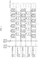
- FIG. 15 is a timing chart for light emission and exposure control in distance measuring device 100 according to the present embodiment.
- the operations of light emission and exposure controller 101 according to the present embodiment make it possible to average signals including background light components subject to fluctuation in intensity of the illumination light. For this reason, it is possible to eliminate an unbalanced amount of the signals including the background light components among S0 exposure, S1 exposure, and BG exposure of the first to fourth pixel groups of solid-state image sensor 102. In particular, it is possible to accurately extract signals including illumination light components in the S0 exposure and S1 exposure of each pixel of the third pixel group or the fourth pixel group having a relatively short exposure time.
- FIG. 14 shows, as the present embodiment, a relationship among the pixel groups referred to when combiner 112 in signal processor 103 performs combination.
- Combiner 112 receives, from line memory 11, signals S0, signals S1, and signals BG of one pixel in the first pixel group, one pixel in the second pixel group, one pixel in the third pixel group, and one pixel in the fourth pixel group, the four pixels being adjacent to each other and included as processing objects in target pixel group C.
- P01, P02, P11, and P12 in FIG. 14 are target pixel group C.
- Combiner 112 sequentially performs a combination process on the group of P03, P04, P13, and P14 and the group of P21, P22, P31, and P32.
- P01, P02, P11, and P12, target pixel group C in FIG. 14 are used as an example.
- FIG. 16 is a schematic block diagram illustrating combiner 112 in distance measuring device 100 according to the present embodiment.
- combiner 112 includes combination calculation processor 1601, first pixel group background light remover 1602, first pixel group saturation determiner 1603, second pixel group background light remover 1604, second pixel group saturation determiner 1605, third pixel group background light remover 1606, third pixel group saturation determiner 1607, fourth pixel group background light remover 1608, and fourth pixel group saturation determiner 1609.
- S0g1 (P01), S1g1 (P01), and BGg1 (P01), which are signal S0, signal S1, and signal BG respectively, are inputted as the pixel signals of one pixel P01 in the first pixel group to first pixel group background light remover 1602 and first pixel group saturation determiner 1603.
- First pixel group background light remover 1602 makes a calculation using Expression 23, and outputs A0g1 (P01) and A1g1 (P01) to combination calculation processor 1601.
- A0g1 P01 S0g1 P01 ⁇ BGg1 P01
- A1g1 P01 S1g1 P01 ⁇ BGg1 P01
- first pixel group saturation determiner 1603 determines the conditions of Expression 24 for saturation determination threshold value Smax. When any of the conditions is satisfied, first pixel group saturation determiner 1603 informs combination calculation processor 1601 about the presence of a saturation signal. S0g1 P01 > Smax S1g1 P01 > Smax BGg1 P01 > Smax
- Input signals S0g2 (P02), S1g2 (P02), and BGg2 (P02) of pixel P02 in the second pixel group are inputted in the same manner as pixel P01.
- Second pixel group background light remover 1604 calculates and outputs A0g2 (P02) and Alg2 (P02) to combination calculation processor 1601.
- Second pixel group saturation determiner 1605 informs combination calculation processor 1601 about the presence or absence of a saturation signal among S0g2 (P02), S1g2 (P02), and BGg2 (P02).
- Input signals S0g3 (P11), S1g3 (P11), and BGg3 (P11) of pixel P11 in the third pixel group are inputted in the same manner as pixel P01.
- Third pixel group background light remover 1606 calculates and outputs A0g3 (P11) and A1g3 (P11) to combination calculation processor 1601.
- Third pixel group saturation determiner 1607 informs combination calculation processor 1601 about the presence or absence of a saturation signal among S0g3 (P11), S1g3 (P11), and BGg3 (P11).
- Input signals S0g4 (P12), S1g4 (P12), and BGg4 (P12) of pixel P12 in the fourth pixel group are inputted in the same manner as pixel P01.
- Fourth pixel group background light remover 1608 calculates and outputs A0g4 (P12) and A1g4 (P12) to combination calculation processor 1601.
- Fourth pixel group saturation determiner 1609 informs combination calculation processor 1601 about the presence or absence of a saturation signal among S0g4 (P12), S1g4 (P12), and BGg4 (P12).
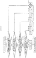
- FIG. 17 is a flowchart illustrating the steps of combination calculation in distance measuring device 100 according to the present embodiment.
- fourth pixel group saturation determiner 1609 determines whether a saturation signal is present (Step S1701). When the saturation signal is determined to be present (Y in Step S1701), fourth pixel group saturation determiner 1609 informs combination calculation processor 1601 about the presence of the saturation signal. In this case, combination calculation processor 1601 performs a distance unmeasurable process (Step S1705).
- combination calculation processor 1601 outputs a distance unmeasurable state to distance calculator 113.
- third pixel group saturation determiner 1607 determines whether a saturation signal is present (Step S1702). When the saturation signal is determined to be present (Y in Step S1702), third pixel group saturation determiner 1607 informs combination calculation processor 1601 about the presence of the saturation signal. In this case, combination calculation processor 1601 performs combination calculation 4 (Step S1706).
- second pixel group saturation determiner 1605 determines whether a saturation signal is present (Step S1703). When the saturation signal is determined to be present (Y in Step S1703), second pixel group saturation determiner 1605 informs combination calculation processor 1601 about the presence of the saturation signal. In this case, combination calculation processor 1601 performs combination calculation 3 (Step S1707).
- first pixel group saturation determiner 1603 determines whether a saturation signal is present (Step S1704). When the saturation signal is determined to be present (Y in Step S1704), first pixel group saturation determiner 1603 informs combination calculation processor 1601 about the presence of the saturation signal. In this case, combination calculation processor 1601 performs combination calculation 2 (Step S1708).
- combination calculation processor 1601 When the saturation signal is determined to be absent (N in Step S1704), combination calculation processor 1601 performs combination calculation 1. In combination calculation 1, since signals are inputted from solid-state image sensor 102 within a normal signal range in which all pixels to be processed are in an unsaturation state, combination calculation processor 1601 makes a calculation using Expression 25, and outputs AOmix and A1mix to distance calculator 113.
- A0mix A0g1 P01 + A0g2 P02 + A0g3 P11 + A0g4 P12
- A1mix A1g1 P01 + A1g2 P02 + A1g3 P11 + A1g4 P12
- output signal AOmix has an amount of signal fifteen times greater than that of signal A0g4 of P12 having the shortest exposure time.
- output signal Almix has an amount of signal fifteen times greater than that of signal A1g4 of P12.
- combination calculation processor 1601 excludes the pixel signal of P01, makes a calculation using Expression 26, and outputs AOmix and Almix to distance calculator 113.
- A0mix A0g2 P02 + A0g3 P11 + A0g4 P12
- A1mix A1g2 P02 + A1g3 P11 + A1g4 P12
- combination calculation processor 1601 excludes the pixel signals of P01 and P02, makes a calculation using Expression 27, and outputs AOmix and Almix to distance calculator 113.
- A0mix A0g3 P11 + A0g4 P12
- A1mix A1g3 P11 + A1g4 P12
- combination calculation 4 the signal is outputted from solid-state image sensor 102 within a normal signal range in which, among the pixels to be processed, only P12 in the fourth pixel group is in an unsaturation state. Accordingly, combination calculation processor 1601 makes a calculation using Expression 28, and outputs AOmix and Almix to distance calculator 113.
- a 0 mix A 0 g 4 P 12
- a 1 mix A 1 g 4 P 12
- distance calculator 113 operates in the same manner in Embodiments 1 and 2.
- the independent exposure control of the four pixel groups makes it possible to expand the signal range of solid-state image sensor 102 by eight times.
- distance measuring device 100 according to the present embodiment can expand a distance measurement range by slightly less than three times in terms of distance, compared to distance measuring device 100 according to Embodiment 1.
- the exposure time ratio of the four pixel groups is not limited to the ratio described in Embodiment 2, the exposure time ratio can be easily changed by changing the timings of exposure timing signals generated by light emission and exposure controller 101.
- the number of pixel groups on which distance measuring device 100 according to Embodiment 2 performs exposure time control independently is four, it is possible to easily further increase the number of pixel groups on which exposure control is performed independently, by increasing the number of exposure timing signals generated by light emission and exposure controller 101, and increasing the number of division lines to the pixel cells in solid-state image sensor 102 for the exposure timing signals.
- a distance measuring device can be achieved that (i) expands the distance measurement range of a solid-state image sensor within one frame, which is restricted by the attenuation of light caused by a distance to an object or a decrease in intensity of reflected light caused by the surface reflectance of the object, (ii) is unaffected when the distance to the object changes in a temporal direction, (iii) is capable of removing the influence of disturbance caused by background light other than radiation light, and (iv) is further capable of obtaining a distance image having reasonable accuracy. Further, a distance measuring device can be achieved that does not require a frame memory or the like, is small, and costs low.
- the present disclosure is applicable to, for example, devices that detect the presence of a person, such as vehicle-mounted passenger detection devices, monitoring devices for industrial factory automation (FA), and input devices that three-dimensionally detect the motion of arms or fingers of a person to recognize a gesture of the person, and receive a user interface input for a specific device including a PC.
- devices that detect the presence of a person such as vehicle-mounted passenger detection devices, monitoring devices for industrial factory automation (FA), and input devices that three-dimensionally detect the motion of arms or fingers of a person to recognize a gesture of the person, and receive a user interface input for a specific device including a PC.
- FA industrial factory automation
Landscapes
- Physics & Mathematics (AREA)
- Engineering & Computer Science (AREA)
- General Physics & Mathematics (AREA)
- Radar, Positioning & Navigation (AREA)
- Remote Sensing (AREA)
- Computer Networks & Wireless Communication (AREA)
- Electromagnetism (AREA)
- Optics & Photonics (AREA)
- Optical Radar Systems And Details Thereof (AREA)
- Measurement Of Optical Distance (AREA)
Claims (9)
- Dispositif de mesure de distance (100) qui mesure une distance par rapport à un objet, à l'aide d'un temps de propagation d'aller-retour de la lumière, le dispositif de mesure de distance comprenant :un émetteur de lumière (104) comportant une source de lumière qui émet de la lumière vers une plage de mesure cible ;un capteur d'image à semi-conducteurs (102) qui comporte une pluralité de pixels inclus dans une pluralité de groupes de pixels aptes à être exposés de manière indépendante, et qui fait effectuer à la pluralité de pixels une conversion photoélectrique de la lumière réfléchie par l'objet dans un angle de vue de la lumière de rayonnement provenant de l'émetteur de lumière, la pluralité de pixels étant agencée en une matrice ;un dispositif de commande d'émission de lumière et d'exposition (101) qui (i) donne une instruction de positionnement temporel d'émission de lumière et de période d'émission de lumière de la source de lumière, à l'émetteur de lumière, (ii) donne, à chaque groupe de la pluralité de groupes de pixels dans le capteur d'image à semi-conducteurs, une instruction de positionnement temporel d'exposition et de période d'exposition pour obtenir des signaux de pixels de types correspondant à une différence de temps entre la lumière de rayonnement et la lumière réfléchie due à un temps de propagation d'aller-retour de la lumière, etcaractérisé en ce que :en outre, le dispositif de commande d'émission de lumière et d'exposition (iii) expose de manière intermittente la pluralité de pixels en exposant chaque groupe de la pluralité de groupes de pixels à un temps d'exposition différent dans au moins deux périodes d'exposition cyclique (S0, S1) correspondant à l'émission d'une lumière de rayonnement et une période d'exposition cyclique (BG) lorsqu'aucune lumière de rayonnement n'est émise, lesdites périodes d'exposition étant comprises dans une période de cycle, Tbg, de la source de lumière qui est comprise dans un dispositif d'éclairage recevant une puissance d'une source commerciale de courant alternatif, faisant fluctuer cycliquement et émettant une lumière de fond dans un cycle de fluctuation de lumière de fond en fonction du positionnement temporel d'exposition et de la période d'exposition, les signaux de pixels des types correspondant à la différence de temps entre la lumière de rayonnement et la lumière réfléchie, etdans lequel, lorsqu'un cycle de la période d'exposition pour chacun des signaux de pixels de la pluralité de groupes de pixels dans le capteur d'image à semi-conducteurs est désigné Tcyc, et que le nombre de périodes d'exposition au sein d'une trame est désigné Ncyc, Tcyc est environ égal à 1/n par rapport à la période de cycle Tbg de la source de lumière, le temps Tcyc x Ncyc qui est nécessaire à l'exposition et qui comprend une période de repos est environ égal à m fois la période de cycle Tbg, n étant un entier naturel supérieur ou égal à 2, m étant un entier naturel supérieur ou égal à 1 ; et le dispositif de mesure de distance (100) comprend en outre :
un processeur de signaux (103) qui calcule une valeur de distance de l'objet dont une image est formée par le capteur d'image à semi-conducteurs, en fonction de signaux de pixels d'au moins deux pixels adjacents exposés aux différents temps d'exposition pour chaque groupe de la pluralité de groupes de pixels dans le capteur d'image à semi-conducteurs, les signaux de pixels correspondant à la différence de temps. - Dispositif de mesure de distance (100) selon la revendication 1,
dans lequel le processeur de signaux comporte :un combineur (112) qui combine les signaux de pixels des au moins deux pixels adjacents en un signal de pixel combiné correspondant à la différence de temps ; etun calculateur de distance (113) qui calcule la valeur de distance de l'objet à partir du signal de pixel combiné, en fonction de la différence de temps entre la lumière de rayonnement et la lumière réfléchie. - Dispositif de mesure de distance (100) selon la revendication 1 ou 2,
dans lequel, dans le capteur d'image à semi-conducteurs (102), au moins deux groupes de la pluralité de groupes de pixels comprennent un premier groupe de pixels et un second groupe de pixels, les au moins deux groupes de la pluralité de groupes de pixels étant aptes à être exposés de manière indépendante, le premier groupe de pixels comprenant, parmi la pluralité de pixels dans le capteur d'image à semi-conducteurs, des pixels dans des rangées impaires, le second groupe de pixels comprenant, parmi la pluralité de pixels dans le capteur d'image à semi-conducteurs, des pixels dans des rangées paires. - Dispositif de mesure de distance (100) selon la revendication 1 ou 2,
dans lequel, dans le capteur d'image à semi-conducteurs (102), au moins deux groupes de la pluralité de groupes de pixels comprennent un premier groupe de pixels, un deuxième groupe de pixels, un troisième groupe de pixels et un quatrième groupe de pixels, les au moins deux groupes de la pluralité de groupes de pixels étant aptes à être exposés de manière indépendante, le premier groupe de pixels comprenant, parmi la pluralité de pixels dans le capteur d'image à semi-conducteurs, des pixels dans des rangées paires et des colonnes paires, le deuxième groupe de pixels comprenant, parmi la pluralité de pixels dans le capteur d'image à semi-conducteurs, des pixels dans les rangées paires et les colonnes impaires, le troisième groupe de pixels comprenant, parmi la pluralité de pixels dans le capteur d'image à semi-conducteurs, des pixels dans des rangées impaires et les colonnes paires, le quatrième groupe de pixels comprenant, parmi la pluralité de pixels dans le capteur d'image à semi-conducteurs, des pixels dans les rangées impaires et les colonnes impaires. - Dispositif de mesure de distance (100) selon la revendication 2,
dans lequel le combineur (112) (i) détermine si chacun des signaux de pixels des au moins deux pixels adjacents est saturé, (ii) exclut, lorsqu'au moins l'un des signaux de pixels des au moins deux pixels adjacents est déterminé comme étant saturé, le au moins un signal de pixel déterminé comme étant saturé, et (iii) obtient le signal de pixel combiné. - Dispositif de mesure de distance (100) selon la revendication 5,
dans lequel, lorsque le au moins un signal de pixel est déterminé comme étant saturé, le combineur (112) interpole le au moins un signal déterminé comme étant saturé, en multipliant, parmi les signaux de pixels des au moins deux pixels adjacents, un signal de pixel déterminé comme étant insaturé par un facteur d'échelle entre un temps d'exposition correspondant au au moins un signal de pixel déterminé comme étant saturé et un temps d'exposition correspondant au signal de pixel déterminé comme étant insaturé, et combine le au moins un signal de pixel interpolé. - Dispositif de mesure de distance (100) selon la revendication 1 ou 2,
dans lequel le dispositif de commande d'émission de lumière et d'exposition (101) commande le capteur d'image à semi-conducteurs (102) de manière que dans une période d'exposition intermittente pour chacun des signaux de pixels de la pluralité de groupes de pixels dans le capteur d'image à semi-conducteurs, une période d'exposition d'un groupe de la pluralité de groupes de pixels chevauche temporellement une période d'exposition d'un autre groupe de la pluralité de groupes de pixels, la période d'exposition intermittente correspondant à la différence de temps entre la lumière de rayonnement et la lumière réfléchie, la période d'exposition de l'autre groupe de la pluralité de groupes de pixels étant relativement plus courte que la période d'exposition du premier groupe de la pluralité de groupes de pixels. - Dispositif de mesure de distance (100) selon la revendication 1 ou 2,dans lequel le dispositif de commande d'émission de lumière et d'exposition (101) commande le capteur d'image à semi-conducteurs (102) de manière que dans une période d'exposition pour au moins l'un des signaux de pixels de la pluralité de groupes de pixels, la conversion photoélectrique de la seule lumière de fond ait pour résultat un signal de pixel, en réglant un positionnement temporel d'exposition auquel la lumière réfléchie par l'objet n'est pas incidente sur le capteur d'image à semi-conducteurs, la période d'exposition du au moins un des signaux de pixels étant incluse dans une période d'exposition intermittente pour chacun des signaux de pixels, la période d'exposition intermittente correspondant à la différence de temps entre la lumière de rayonnement et la lumière réfléchie, etle combineur (112) exclut une composante de lumière de fond d'un signal de pixel qui est au moins l'un des signaux de pixels des deux pixels adjacents et inclut à la fois une composante de lumière de rayonnement et la composante de lumière de fond, en utilisant le signal de pixel n'incluant que la composante de lumière de fond.
- Dispositif de mesure de distance (100) selon la revendication 1 ou 2,dans lequel le capteur d'image à semi-conducteurs (102) comporte : une photodiode (501) qui effectue une conversion photoélectrique sur la pluralité de pixels ; une pluralité de mémoires analogiques (520, 521, 522) qui accumulent et conservent sélectivement des charges électriques générées du fait de la conversion photoélectrique par la photodiode ; et un obturateur électronique qui rejette, pour toute la pluralité de pixels, les charges électriques générées par la photodiode, l'accumulation et la conservation sélectives des charges électriques générées par la photodiode étant communes à chaque groupe de la pluralité de groupes de pixels,le dispositif de commande d'émission de lumière et d'exposition (101) donne l'instruction de la commande de commutation de l'obturateur électronique dans le capteur d'image à semi-conducteurs, et de la commande de l'accumulation et de la conservation sélectives des charges électriques dans chaque mémoire de la pluralité de mémoires analogiques pour un groupe correspondant de la pluralité de groupes de pixels, etle dispositif de commande d'émission de lumière et d'exposition (101) fait en sorte que l'émetteur de lumière (104) émette de multiples fois de la lumière de rayonnement pulsée, commande la commutation de l'obturateur électronique qui génère une impulsion synchronisée avec la lumière de rayonnement pulsée et ayant une phase différente d'une phase de la lumière de rayonnement pulsée, donne, à une mémoire prédéterminée de la pluralité de mémoires analogiques pour un groupe prédéterminé de la pluralité de groupes de pixels dans le capteur d'image à semi-conducteurs, l'instruction d'accumuler des charges électriques au cours d'une période de commande de l'obturateur électronique qui génère l'impulsion ayant une phase identique à une phase de la lumière de rayonnement pulsée, et commande le capteur d'image à semi-conducteurs (102) de manière que le temps d'exposition différent de chaque groupe de la pluralité de groupes de pixels dans le capteur d'image à semi-conducteurs soit généré en fonction d'une différence de longueur d'une période de l'accumulation des charges électriques correspondant au nombre de fois où la lumière de rayonnement pulsée est émise de manière répétée.
Applications Claiming Priority (2)
| Application Number | Priority Date | Filing Date | Title |
|---|---|---|---|
| JP2016230890 | 2016-11-29 | ||
| PCT/JP2017/042318 WO2018101187A1 (fr) | 2016-11-29 | 2017-11-27 | Dispositif de mesure de distance |
Publications (3)
| Publication Number | Publication Date |
|---|---|
| EP3550330A1 EP3550330A1 (fr) | 2019-10-09 |
| EP3550330A4 EP3550330A4 (fr) | 2019-10-30 |
| EP3550330B1 true EP3550330B1 (fr) | 2022-05-04 |
Family
ID=62242659
Family Applications (1)
| Application Number | Title | Priority Date | Filing Date |
|---|---|---|---|
| EP17876971.7A Active EP3550330B1 (fr) | 2016-11-29 | 2017-11-27 | Dispositif de mesure de distance |
Country Status (5)
| Country | Link |
|---|---|
| US (1) | US11448757B2 (fr) |
| EP (1) | EP3550330B1 (fr) |
| JP (1) | JP6981997B2 (fr) |
| CN (1) | CN110023785B (fr) |
| WO (1) | WO2018101187A1 (fr) |
Families Citing this family (31)
| Publication number | Priority date | Publication date | Assignee | Title |
|---|---|---|---|---|
| WO2014018949A2 (fr) * | 2012-07-26 | 2014-01-30 | Olive Medical Corporation | Obtention d'une gamme dynamique large au moyen d'un capteur monochromatique |
| US11585898B2 (en) * | 2017-01-13 | 2023-02-21 | Sony Group Corporation | Signal processing device, signal processing method, and program |
| DE102018205378A1 (de) * | 2018-04-10 | 2019-10-10 | Ibeo Automotive Systems GmbH | Verfahren zur Ansteuerung von Sensorelementen eines LIDAR Messsystems |
| US11092678B2 (en) * | 2018-06-21 | 2021-08-17 | Analog Devices, Inc. | Measuring and removing the corruption of time-of-flight depth images due to internal scattering |
| JP7402160B2 (ja) * | 2018-07-23 | 2023-12-20 | ヌヴォトンテクノロジージャパン株式会社 | 距離測定装置および信頼性判定方法 |
| US11294039B2 (en) * | 2018-07-24 | 2022-04-05 | Samsung Electronics Co., Ltd. | Time-resolving image sensor for range measurement and 2D greyscale imaging |
| WO2020080065A1 (fr) * | 2018-10-16 | 2020-04-23 | 株式会社ブルックマンテクノロジ | Dispositif de mesure de distance, appareil de prise de vues et procédé de réglage de l'entraînement d'un dispositif de mesure de distance |
| US11506763B2 (en) * | 2018-10-31 | 2022-11-22 | Infineon Technologies Ag | Image sensor with interleaved hold for single-readout depth measurement |
| EP3663801B1 (fr) | 2018-12-07 | 2022-09-28 | Infineon Technologies AG | Module de capteur de durée de vol, procédé, appareil et programme informatique pour déterminer des informations de distance sur la base de données de capteur de durée de vol |
| KR102646902B1 (ko) * | 2019-02-12 | 2024-03-12 | 삼성전자주식회사 | 거리 측정을 위한 이미지 센서 |
| JP7209198B2 (ja) * | 2019-03-27 | 2023-01-20 | パナソニックIpマネジメント株式会社 | 距離測定装置および画像生成方法 |
| WO2020195046A1 (fr) * | 2019-03-27 | 2020-10-01 | パナソニックIpマネジメント株式会社 | Dispositif d'imagerie à semi-conducteurs |
| JP7472902B2 (ja) * | 2019-03-29 | 2024-04-23 | Toppanホールディングス株式会社 | 固体撮像装置、撮像システム及び撮像方法 |
| JP2020193957A (ja) * | 2019-05-30 | 2020-12-03 | ファナック株式会社 | 測距異常を補正する距離画像生成装置 |
| KR102858186B1 (ko) * | 2019-09-20 | 2025-09-10 | 엘지이노텍 주식회사 | 카메라 모듈 |
| TWI877189B (zh) * | 2019-09-27 | 2025-03-21 | 日商索尼半導體解決方案公司 | 資訊處理裝置、修正方法及程式 |
| US11726186B2 (en) * | 2019-09-30 | 2023-08-15 | Zoox, Inc. | Pixel filtering using multiple exposures |
| US11841438B2 (en) | 2019-09-30 | 2023-12-12 | Zoox, Inc. | Power control of sensors using multiple exposures |
| JP7235638B2 (ja) * | 2019-10-04 | 2023-03-08 | 株式会社日立エルジーデータストレージ | 測距装置および測距システム |
| JP7469779B2 (ja) * | 2019-10-10 | 2024-04-17 | Toppanホールディングス株式会社 | 距離画像撮像装置、及び距離画像撮像方法 |
| KR20210072458A (ko) * | 2019-12-09 | 2021-06-17 | 에스케이하이닉스 주식회사 | 비행시간거리측정 방식의 센싱 시스템 및 이미지 센서 |
| CN111175774B (zh) * | 2020-01-14 | 2022-09-09 | 炬佑智能科技(苏州)有限公司 | 一种tof传感器模块的控制方法 |
| EP4121794A1 (fr) | 2020-03-18 | 2023-01-25 | Ricoh Company, Ltd. | Appareil de mesure de distance et procédé de mesure de distance |
| WO2021193646A1 (fr) * | 2020-03-26 | 2021-09-30 | 株式会社小糸製作所 | Dispositif d'imagerie, éclairage de véhicule et véhicule |
| US12306349B2 (en) | 2020-05-15 | 2025-05-20 | Analog Devices International Unlimited Company | Proximity detection system |
| CN112954230B (zh) * | 2021-02-08 | 2022-09-09 | 深圳市汇顶科技股份有限公司 | 深度测量方法、芯片和电子设备 |
| CN113296114B (zh) * | 2021-05-21 | 2024-05-14 | Oppo广东移动通信有限公司 | dTOF深度图像的采集方法、装置、电子设备及介质 |
| CN115480258B (zh) * | 2021-05-31 | 2024-11-05 | 宁波飞芯电子科技有限公司 | 一种探测装置及方法 |
| CN117368885A (zh) * | 2021-08-23 | 2024-01-09 | 深圳市速腾聚创科技有限公司 | 一种雷达数据处理方法、终端设备及计算机可读存储介质 |
| CN116008949B (zh) * | 2021-10-22 | 2024-02-27 | 深圳市速腾聚创科技有限公司 | 一种雷达数据处理方法、终端设备及计算机可读存储介质 |
| US20260032795A1 (en) * | 2024-07-25 | 2026-01-29 | AeroClenz, Inc. | System for controlling uv-c led |
Family Cites Families (29)
| Publication number | Priority date | Publication date | Assignee | Title |
|---|---|---|---|---|
| JP4161910B2 (ja) * | 2004-01-28 | 2008-10-08 | 株式会社デンソー | 距離画像データ生成装置及び生成方法,プログラム |
| JP2006253876A (ja) | 2005-03-09 | 2006-09-21 | Sony Corp | 物理量分布検知装置および物理量分布検知装置の駆動方法 |
| JP4998056B2 (ja) * | 2006-05-11 | 2012-08-15 | セイコーエプソン株式会社 | 撮像装置、撮像システム及び撮像方法 |
| JP4981780B2 (ja) * | 2008-10-20 | 2012-07-25 | 本田技研工業株式会社 | 測距システム及び測距方法 |
| JP2010114674A (ja) * | 2008-11-06 | 2010-05-20 | Sanyo Electric Co Ltd | ビデオカメラ |
| JP2010166246A (ja) * | 2009-01-14 | 2010-07-29 | Fujifilm Corp | 撮像装置及び撮像制御方法 |
| JP5743390B2 (ja) | 2009-09-15 | 2015-07-01 | 本田技研工業株式会社 | 測距装置、及び測距方法 |
| JP5713816B2 (ja) * | 2011-03-16 | 2015-05-07 | 株式会社東芝 | 固体撮像装置及びカメラモジュール |
| JP2012225807A (ja) | 2011-04-20 | 2012-11-15 | Optex Co Ltd | 距離画像カメラおよび距離画像合成方法 |
| EP2740008A4 (fr) * | 2011-08-02 | 2015-09-16 | Hewlett Packard Development Co | Système et procédé d'acquisition de projection |
| WO2013051186A1 (fr) * | 2011-10-03 | 2013-04-11 | パナソニック株式会社 | Dispositif de formation d'image, système utilisant ledit dispositif de formation d'image et dispositif de mesure de distance |
| JP5794176B2 (ja) * | 2012-03-02 | 2015-10-14 | カシオ計算機株式会社 | 撮像装置、撮像方法及びプログラム |
| EP2825867B1 (fr) * | 2012-03-15 | 2020-01-01 | Bio-Rad Laboratories, Inc. | Acquisition d'image pour échantillons chimioluminescents |
| WO2013146311A1 (fr) * | 2012-03-28 | 2013-10-03 | 富士フイルム株式会社 | Dispositif d'imagerie et dispositif endoscopique équipé de celui-ci |
| JP2013219708A (ja) * | 2012-04-12 | 2013-10-24 | Sony Corp | 画像処理装置、および画像処理方法、並びにプログラム |
| JP6296697B2 (ja) * | 2013-05-10 | 2018-03-20 | キヤノン株式会社 | 撮像装置、制御方法、プログラム及び記憶媒体 |
| WO2015025497A1 (fr) * | 2013-08-23 | 2015-02-26 | パナソニックIpマネジメント株式会社 | Système de mesure de la distance et dispositif de génération de signaux |
| US10063844B2 (en) * | 2013-10-17 | 2018-08-28 | Microsoft Technology Licensing, Llc. | Determining distances by probabilistic time of flight imaging |
| US9473706B2 (en) * | 2013-12-09 | 2016-10-18 | Apple Inc. | Image sensor flicker detection |
| JP6408372B2 (ja) * | 2014-03-31 | 2018-10-17 | ソニーセミコンダクタソリューションズ株式会社 | 固体撮像装置及びその駆動制御方法、並びに、電子機器 |
| KR102409952B1 (ko) * | 2014-04-07 | 2022-06-17 | 삼성전자주식회사 | 고해상도, 고프레임률, 저전력 이미지 센서 |
| JP6537224B2 (ja) * | 2014-04-23 | 2019-07-03 | キヤノン株式会社 | 撮像装置、制御方法、プログラム及び記憶媒体 |
| JP6755799B2 (ja) * | 2014-08-29 | 2020-09-16 | パナソニックセミコンダクターソリューションズ株式会社 | 撮像装置、及びそれに用いられる固体撮像装置 |
| JP6424581B2 (ja) * | 2014-11-21 | 2018-11-21 | 株式会社デンソー | 光飛行型測距装置 |
| JP6539990B2 (ja) * | 2014-11-14 | 2019-07-10 | 株式会社デンソー | 光飛行型測距装置 |
| WO2016075945A1 (fr) * | 2014-11-14 | 2016-05-19 | 株式会社デンソー | Dispositif de télémétrie optique par mesure du temps de vol |
| US9881235B1 (en) * | 2014-11-21 | 2018-01-30 | Mahmoud Narimanzadeh | System, apparatus, and method for determining physical dimensions in digital images |
| CN105872392B (zh) * | 2015-01-23 | 2019-01-04 | 原相科技股份有限公司 | 具有动态曝光时间的光学测距系统 |
| US9659371B2 (en) * | 2015-10-08 | 2017-05-23 | Christie Digital Systems Usa, Inc. | System and method for online projector-camera calibration from one or more images |
-
2017
- 2017-11-27 EP EP17876971.7A patent/EP3550330B1/fr active Active
- 2017-11-27 JP JP2018553826A patent/JP6981997B2/ja active Active
- 2017-11-27 US US16/464,238 patent/US11448757B2/en active Active
- 2017-11-27 WO PCT/JP2017/042318 patent/WO2018101187A1/fr not_active Ceased
- 2017-11-27 CN CN201780072791.0A patent/CN110023785B/zh active Active
Also Published As
| Publication number | Publication date |
|---|---|
| CN110023785A (zh) | 2019-07-16 |
| US20190391266A1 (en) | 2019-12-26 |
| US11448757B2 (en) | 2022-09-20 |
| JP6981997B2 (ja) | 2021-12-17 |
| WO2018101187A1 (fr) | 2018-06-07 |
| EP3550330A4 (fr) | 2019-10-30 |
| CN110023785B (zh) | 2023-03-28 |
| JPWO2018101187A1 (ja) | 2019-10-24 |
| EP3550330A1 (fr) | 2019-10-09 |
Similar Documents
| Publication | Publication Date | Title |
|---|---|---|
| EP3550330B1 (fr) | Dispositif de mesure de distance | |
| US11378690B2 (en) | Time of flight sensor, a three-dimensional imaging device using the same, and a method for driving the three-dimensional imaging device | |
| US10903254B2 (en) | Distance-measuring imaging device, distance measuring method of distance-measuring imaging device, and solid-state imaging device | |
| US8642938B2 (en) | Shared time of flight pixel | |
| TWI745678B (zh) | 相關的飛行時間感測器 | |
| US9787912B2 (en) | Image capture device | |
| US10491842B2 (en) | Imaging device, a solid-state imaging device for use in the imaging device | |
| US11626446B2 (en) | Pixel circuit and method of operating the same in an always-on mode | |
| CN110024375B (zh) | 固态摄像装置和测距摄像装置 | |
| CN110389351B (zh) | Tof距离传感器、传感阵列及基于tof距离传感器的测距方法 | |
| US20190326347A1 (en) | First photon correlated time-of-flight sensor | |
| EP1825297A1 (fr) | Mesure de profil de surface | |
| KR102887078B1 (ko) | 깊이의 측정 범위에 기초하여 동작하는 센서 및 이를 포함하는 센싱 시스템 | |
| WO2020188782A1 (fr) | Dispositif de capture d'image de distance, système de capture d'image de distance et procédé de capture d'image de distance | |
| JP2018185179A (ja) | 測距装置、監視装置、3次元計測装置、移動体、ロボット及び測距方法 | |
| WO2021113001A1 (fr) | Réseau configurable de détecteurs de photon unique | |
| US20230078063A1 (en) | Distance measurement device and distance measurement system | |
| US20240192370A1 (en) | Distance measuring device and distance measuring system | |
| US12566271B2 (en) | Movement amount estimation device, movement amount estimation method, movement amount estimation program, and movement amount estimation system | |
| US20230204727A1 (en) | Distance measurement device and distance measurement method | |
| US20250184468A1 (en) | Depth Scanning Image Sensor | |
| JP2022021296A (ja) | 光検出システム | |
| CN113597534A (zh) | 测距成像系统、测距成像方法和程序 | |
| JP2014021100A (ja) | 3次元情報検出装置および3次元情報検出方法 | |
| Baranov et al. | Multi-pulse active CCD television system model for 3D imaging |
Legal Events
| Date | Code | Title | Description |
|---|---|---|---|
| STAA | Information on the status of an ep patent application or granted ep patent |
Free format text: STATUS: THE INTERNATIONAL PUBLICATION HAS BEEN MADE |
|
| PUAI | Public reference made under article 153(3) epc to a published international application that has entered the european phase |
Free format text: ORIGINAL CODE: 0009012 |
|
| STAA | Information on the status of an ep patent application or granted ep patent |
Free format text: STATUS: REQUEST FOR EXAMINATION WAS MADE |
|
| 17P | Request for examination filed |
Effective date: 20190524 |
|
| AK | Designated contracting states |
Kind code of ref document: A1 Designated state(s): AL AT BE BG CH CY CZ DE DK EE ES FI FR GB GR HR HU IE IS IT LI LT LU LV MC MK MT NL NO PL PT RO RS SE SI SK SM TR |
|
| AX | Request for extension of the european patent |
Extension state: BA ME |
|
| A4 | Supplementary search report drawn up and despatched |
Effective date: 20190927 |
|
| RIC1 | Information provided on ipc code assigned before grant |
Ipc: G01S 17/10 20060101ALI20190923BHEP Ipc: G01C 3/06 20060101ALI20190923BHEP Ipc: H04N 5/3745 20110101ALI20190923BHEP Ipc: G01S 17/89 20060101AFI20190923BHEP |
|
| DAV | Request for validation of the european patent (deleted) | ||
| DAX | Request for extension of the european patent (deleted) | ||
| RAP1 | Party data changed (applicant data changed or rights of an application transferred) |
Owner name: PANASONIC SEMICONDUCTOR SOLUTIONS CO., LTD. |
|
| STAA | Information on the status of an ep patent application or granted ep patent |
Free format text: STATUS: EXAMINATION IS IN PROGRESS |
|
| 17Q | First examination report despatched |
Effective date: 20210202 |
|
| RAP3 | Party data changed (applicant data changed or rights of an application transferred) |
Owner name: NUVOTON TECHNOLOGY CORPORATION JAPAN |
|
| RAP3 | Party data changed (applicant data changed or rights of an application transferred) |
Owner name: NUVOTON TECHNOLOGY CORPORATION JAPAN |
|
| GRAP | Despatch of communication of intention to grant a patent |
Free format text: ORIGINAL CODE: EPIDOSNIGR1 |
|
| STAA | Information on the status of an ep patent application or granted ep patent |
Free format text: STATUS: GRANT OF PATENT IS INTENDED |
|
| INTG | Intention to grant announced |
Effective date: 20220214 |
|
| GRAS | Grant fee paid |
Free format text: ORIGINAL CODE: EPIDOSNIGR3 |
|
| GRAA | (expected) grant |
Free format text: ORIGINAL CODE: 0009210 |
|
| STAA | Information on the status of an ep patent application or granted ep patent |
Free format text: STATUS: THE PATENT HAS BEEN GRANTED |
|
| AK | Designated contracting states |
Kind code of ref document: B1 Designated state(s): AL AT BE BG CH CY CZ DE DK EE ES FI FR GB GR HR HU IE IS IT LI LT LU LV MC MK MT NL NO PL PT RO RS SE SI SK SM TR |
|
| REG | Reference to a national code |
Ref country code: GB Ref legal event code: FG4D |
|
| REG | Reference to a national code |
Ref country code: CH Ref legal event code: EP |
|
| REG | Reference to a national code |
Ref country code: AT Ref legal event code: REF Ref document number: 1489632 Country of ref document: AT Kind code of ref document: T Effective date: 20220515 |
|
| REG | Reference to a national code |
Ref country code: DE Ref legal event code: R096 Ref document number: 602017057122 Country of ref document: DE |
|
| REG | Reference to a national code |
Ref country code: IE Ref legal event code: FG4D |
|
| REG | Reference to a national code |
Ref country code: LT Ref legal event code: MG9D |
|
| REG | Reference to a national code |
Ref country code: NL Ref legal event code: MP Effective date: 20220504 |
|
| REG | Reference to a national code |
Ref country code: AT Ref legal event code: MK05 Ref document number: 1489632 Country of ref document: AT Kind code of ref document: T Effective date: 20220504 |
|
| PG25 | Lapsed in a contracting state [announced via postgrant information from national office to epo] |
Ref country code: SE Free format text: LAPSE BECAUSE OF FAILURE TO SUBMIT A TRANSLATION OF THE DESCRIPTION OR TO PAY THE FEE WITHIN THE PRESCRIBED TIME-LIMIT Effective date: 20220504 Ref country code: PT Free format text: LAPSE BECAUSE OF FAILURE TO SUBMIT A TRANSLATION OF THE DESCRIPTION OR TO PAY THE FEE WITHIN THE PRESCRIBED TIME-LIMIT Effective date: 20220905 Ref country code: NO Free format text: LAPSE BECAUSE OF FAILURE TO SUBMIT A TRANSLATION OF THE DESCRIPTION OR TO PAY THE FEE WITHIN THE PRESCRIBED TIME-LIMIT Effective date: 20220804 Ref country code: NL Free format text: LAPSE BECAUSE OF FAILURE TO SUBMIT A TRANSLATION OF THE DESCRIPTION OR TO PAY THE FEE WITHIN THE PRESCRIBED TIME-LIMIT Effective date: 20220504 Ref country code: LT Free format text: LAPSE BECAUSE OF FAILURE TO SUBMIT A TRANSLATION OF THE DESCRIPTION OR TO PAY THE FEE WITHIN THE PRESCRIBED TIME-LIMIT Effective date: 20220504 Ref country code: HR Free format text: LAPSE BECAUSE OF FAILURE TO SUBMIT A TRANSLATION OF THE DESCRIPTION OR TO PAY THE FEE WITHIN THE PRESCRIBED TIME-LIMIT Effective date: 20220504 Ref country code: GR Free format text: LAPSE BECAUSE OF FAILURE TO SUBMIT A TRANSLATION OF THE DESCRIPTION OR TO PAY THE FEE WITHIN THE PRESCRIBED TIME-LIMIT Effective date: 20220805 Ref country code: FI Free format text: LAPSE BECAUSE OF FAILURE TO SUBMIT A TRANSLATION OF THE DESCRIPTION OR TO PAY THE FEE WITHIN THE PRESCRIBED TIME-LIMIT Effective date: 20220504 Ref country code: ES Free format text: LAPSE BECAUSE OF FAILURE TO SUBMIT A TRANSLATION OF THE DESCRIPTION OR TO PAY THE FEE WITHIN THE PRESCRIBED TIME-LIMIT Effective date: 20220504 Ref country code: BG Free format text: LAPSE BECAUSE OF FAILURE TO SUBMIT A TRANSLATION OF THE DESCRIPTION OR TO PAY THE FEE WITHIN THE PRESCRIBED TIME-LIMIT Effective date: 20220804 Ref country code: AT Free format text: LAPSE BECAUSE OF FAILURE TO SUBMIT A TRANSLATION OF THE DESCRIPTION OR TO PAY THE FEE WITHIN THE PRESCRIBED TIME-LIMIT Effective date: 20220504 |
|
| PG25 | Lapsed in a contracting state [announced via postgrant information from national office to epo] |
Ref country code: RS Free format text: LAPSE BECAUSE OF FAILURE TO SUBMIT A TRANSLATION OF THE DESCRIPTION OR TO PAY THE FEE WITHIN THE PRESCRIBED TIME-LIMIT Effective date: 20220504 Ref country code: PL Free format text: LAPSE BECAUSE OF FAILURE TO SUBMIT A TRANSLATION OF THE DESCRIPTION OR TO PAY THE FEE WITHIN THE PRESCRIBED TIME-LIMIT Effective date: 20220504 Ref country code: LV Free format text: LAPSE BECAUSE OF FAILURE TO SUBMIT A TRANSLATION OF THE DESCRIPTION OR TO PAY THE FEE WITHIN THE PRESCRIBED TIME-LIMIT Effective date: 20220504 Ref country code: IS Free format text: LAPSE BECAUSE OF FAILURE TO SUBMIT A TRANSLATION OF THE DESCRIPTION OR TO PAY THE FEE WITHIN THE PRESCRIBED TIME-LIMIT Effective date: 20220904 |
|
| PG25 | Lapsed in a contracting state [announced via postgrant information from national office to epo] |
Ref country code: SM Free format text: LAPSE BECAUSE OF FAILURE TO SUBMIT A TRANSLATION OF THE DESCRIPTION OR TO PAY THE FEE WITHIN THE PRESCRIBED TIME-LIMIT Effective date: 20220504 Ref country code: SK Free format text: LAPSE BECAUSE OF FAILURE TO SUBMIT A TRANSLATION OF THE DESCRIPTION OR TO PAY THE FEE WITHIN THE PRESCRIBED TIME-LIMIT Effective date: 20220504 Ref country code: RO Free format text: LAPSE BECAUSE OF FAILURE TO SUBMIT A TRANSLATION OF THE DESCRIPTION OR TO PAY THE FEE WITHIN THE PRESCRIBED TIME-LIMIT Effective date: 20220504 Ref country code: EE Free format text: LAPSE BECAUSE OF FAILURE TO SUBMIT A TRANSLATION OF THE DESCRIPTION OR TO PAY THE FEE WITHIN THE PRESCRIBED TIME-LIMIT Effective date: 20220504 Ref country code: DK Free format text: LAPSE BECAUSE OF FAILURE TO SUBMIT A TRANSLATION OF THE DESCRIPTION OR TO PAY THE FEE WITHIN THE PRESCRIBED TIME-LIMIT Effective date: 20220504 Ref country code: CZ Free format text: LAPSE BECAUSE OF FAILURE TO SUBMIT A TRANSLATION OF THE DESCRIPTION OR TO PAY THE FEE WITHIN THE PRESCRIBED TIME-LIMIT Effective date: 20220504 |
|
| REG | Reference to a national code |
Ref country code: DE Ref legal event code: R097 Ref document number: 602017057122 Country of ref document: DE |
|
| PLBE | No opposition filed within time limit |
Free format text: ORIGINAL CODE: 0009261 |
|
| STAA | Information on the status of an ep patent application or granted ep patent |
Free format text: STATUS: NO OPPOSITION FILED WITHIN TIME LIMIT |
|
| PG25 | Lapsed in a contracting state [announced via postgrant information from national office to epo] |
Ref country code: AL Free format text: LAPSE BECAUSE OF FAILURE TO SUBMIT A TRANSLATION OF THE DESCRIPTION OR TO PAY THE FEE WITHIN THE PRESCRIBED TIME-LIMIT Effective date: 20220504 |
|
| 26N | No opposition filed |
Effective date: 20230207 |
|
| PG25 | Lapsed in a contracting state [announced via postgrant information from national office to epo] |
Ref country code: SI Free format text: LAPSE BECAUSE OF FAILURE TO SUBMIT A TRANSLATION OF THE DESCRIPTION OR TO PAY THE FEE WITHIN THE PRESCRIBED TIME-LIMIT Effective date: 20220504 |
|
| PG25 | Lapsed in a contracting state [announced via postgrant information from national office to epo] |
Ref country code: MC Free format text: LAPSE BECAUSE OF FAILURE TO SUBMIT A TRANSLATION OF THE DESCRIPTION OR TO PAY THE FEE WITHIN THE PRESCRIBED TIME-LIMIT Effective date: 20220504 |
|
| REG | Reference to a national code |
Ref country code: CH Ref legal event code: PL |
|
| GBPC | Gb: european patent ceased through non-payment of renewal fee |
Effective date: 20221127 |
|
| REG | Reference to a national code |
Ref country code: BE Ref legal event code: MM Effective date: 20221130 |
|
| PG25 | Lapsed in a contracting state [announced via postgrant information from national office to epo] |
Ref country code: LI Free format text: LAPSE BECAUSE OF NON-PAYMENT OF DUE FEES Effective date: 20221130 Ref country code: CH Free format text: LAPSE BECAUSE OF NON-PAYMENT OF DUE FEES Effective date: 20221130 |
|
| PG25 | Lapsed in a contracting state [announced via postgrant information from national office to epo] |
Ref country code: LU Free format text: LAPSE BECAUSE OF NON-PAYMENT OF DUE FEES Effective date: 20221127 |
|
| PG25 | Lapsed in a contracting state [announced via postgrant information from national office to epo] |
Ref country code: IE Free format text: LAPSE BECAUSE OF NON-PAYMENT OF DUE FEES Effective date: 20221127 Ref country code: GB Free format text: LAPSE BECAUSE OF NON-PAYMENT OF DUE FEES Effective date: 20221127 |
|
| PG25 | Lapsed in a contracting state [announced via postgrant information from national office to epo] |
Ref country code: FR Free format text: LAPSE BECAUSE OF NON-PAYMENT OF DUE FEES Effective date: 20221130 Ref country code: BE Free format text: LAPSE BECAUSE OF NON-PAYMENT OF DUE FEES Effective date: 20221130 |
|
| PG25 | Lapsed in a contracting state [announced via postgrant information from national office to epo] |
Ref country code: IT Free format text: LAPSE BECAUSE OF FAILURE TO SUBMIT A TRANSLATION OF THE DESCRIPTION OR TO PAY THE FEE WITHIN THE PRESCRIBED TIME-LIMIT Effective date: 20220504 |
|
| PG25 | Lapsed in a contracting state [announced via postgrant information from national office to epo] |
Ref country code: HU Free format text: LAPSE BECAUSE OF FAILURE TO SUBMIT A TRANSLATION OF THE DESCRIPTION OR TO PAY THE FEE WITHIN THE PRESCRIBED TIME-LIMIT; INVALID AB INITIO Effective date: 20171127 |
|
| PG25 | Lapsed in a contracting state [announced via postgrant information from national office to epo] |
Ref country code: CY Free format text: LAPSE BECAUSE OF FAILURE TO SUBMIT A TRANSLATION OF THE DESCRIPTION OR TO PAY THE FEE WITHIN THE PRESCRIBED TIME-LIMIT Effective date: 20220504 |
|
| PG25 | Lapsed in a contracting state [announced via postgrant information from national office to epo] |
Ref country code: MK Free format text: LAPSE BECAUSE OF FAILURE TO SUBMIT A TRANSLATION OF THE DESCRIPTION OR TO PAY THE FEE WITHIN THE PRESCRIBED TIME-LIMIT Effective date: 20220504 |
|
| PG25 | Lapsed in a contracting state [announced via postgrant information from national office to epo] |
Ref country code: MT Free format text: LAPSE BECAUSE OF FAILURE TO SUBMIT A TRANSLATION OF THE DESCRIPTION OR TO PAY THE FEE WITHIN THE PRESCRIBED TIME-LIMIT Effective date: 20220504 |
|
| PG25 | Lapsed in a contracting state [announced via postgrant information from national office to epo] |
Ref country code: BG Free format text: LAPSE BECAUSE OF FAILURE TO SUBMIT A TRANSLATION OF THE DESCRIPTION OR TO PAY THE FEE WITHIN THE PRESCRIBED TIME-LIMIT Effective date: 20220504 |
|
| PG25 | Lapsed in a contracting state [announced via postgrant information from national office to epo] |
Ref country code: BG Free format text: LAPSE BECAUSE OF FAILURE TO SUBMIT A TRANSLATION OF THE DESCRIPTION OR TO PAY THE FEE WITHIN THE PRESCRIBED TIME-LIMIT Effective date: 20220504 |
|
| PGFP | Annual fee paid to national office [announced via postgrant information from national office to epo] |
Ref country code: DE Payment date: 20241001 Year of fee payment: 8 |
|
| PG25 | Lapsed in a contracting state [announced via postgrant information from national office to epo] |
Ref country code: TR Free format text: LAPSE BECAUSE OF FAILURE TO SUBMIT A TRANSLATION OF THE DESCRIPTION OR TO PAY THE FEE WITHIN THE PRESCRIBED TIME-LIMIT Effective date: 20220504 |