EP3552463B1 - Assemblage de cartes de circuits imprimés et son procédé de fabrication - Google Patents
Assemblage de cartes de circuits imprimés et son procédé de fabrication Download PDFInfo
- Publication number
- EP3552463B1 EP3552463B1 EP17816673.2A EP17816673A EP3552463B1 EP 3552463 B1 EP3552463 B1 EP 3552463B1 EP 17816673 A EP17816673 A EP 17816673A EP 3552463 B1 EP3552463 B1 EP 3552463B1
- Authority
- EP
- European Patent Office
- Prior art keywords
- printed circuit
- circuit board
- groove
- circuit boards
- boards
- Prior art date
- Legal status (The legal status is an assumption and is not a legal conclusion. Google has not performed a legal analysis and makes no representation as to the accuracy of the status listed.)
- Active
Links
Images



Classifications
-
- H—ELECTRICITY
- H05—ELECTRIC TECHNIQUES NOT OTHERWISE PROVIDED FOR
- H05K—PRINTED CIRCUITS; CASINGS OR CONSTRUCTIONAL DETAILS OF ELECTRIC APPARATUS; MANUFACTURE OF ASSEMBLAGES OF ELECTRICAL COMPONENTS
- H05K3/00—Apparatus or processes for manufacturing printed circuits
- H05K3/36—Assembling printed circuits with other printed circuits
- H05K3/366—Assembling printed circuits with other printed circuits substantially perpendicularly to each other
-
- H—ELECTRICITY
- H05—ELECTRIC TECHNIQUES NOT OTHERWISE PROVIDED FOR
- H05K—PRINTED CIRCUITS; CASINGS OR CONSTRUCTIONAL DETAILS OF ELECTRIC APPARATUS; MANUFACTURE OF ASSEMBLAGES OF ELECTRICAL COMPONENTS
- H05K1/00—Printed circuits
- H05K1/02—Details
- H05K1/14—Structural association of two or more printed circuits
- H05K1/141—One or more single auxiliary printed circuits mounted on a main printed circuit, e.g. modules, adapters
-
- H—ELECTRICITY
- H05—ELECTRIC TECHNIQUES NOT OTHERWISE PROVIDED FOR
- H05K—PRINTED CIRCUITS; CASINGS OR CONSTRUCTIONAL DETAILS OF ELECTRIC APPARATUS; MANUFACTURE OF ASSEMBLAGES OF ELECTRICAL COMPONENTS
- H05K1/00—Printed circuits
- H05K1/02—Details
- H05K1/14—Structural association of two or more printed circuits
-
- H—ELECTRICITY
- H05—ELECTRIC TECHNIQUES NOT OTHERWISE PROVIDED FOR
- H05K—PRINTED CIRCUITS; CASINGS OR CONSTRUCTIONAL DETAILS OF ELECTRIC APPARATUS; MANUFACTURE OF ASSEMBLAGES OF ELECTRICAL COMPONENTS
- H05K2201/00—Indexing scheme relating to printed circuits covered by H05K1/00
- H05K2201/04—Assemblies of printed circuits
- H05K2201/048—Second PCB mounted on first PCB by inserting in window or holes of the first PCB
-
- H—ELECTRICITY
- H05—ELECTRIC TECHNIQUES NOT OTHERWISE PROVIDED FOR
- H05K—PRINTED CIRCUITS; CASINGS OR CONSTRUCTIONAL DETAILS OF ELECTRIC APPARATUS; MANUFACTURE OF ASSEMBLAGES OF ELECTRICAL COMPONENTS
- H05K2201/00—Indexing scheme relating to printed circuits covered by H05K1/00
- H05K2201/09—Shape and layout
- H05K2201/09145—Edge details
-
- H—ELECTRICITY
- H05—ELECTRIC TECHNIQUES NOT OTHERWISE PROVIDED FOR
- H05K—PRINTED CIRCUITS; CASINGS OR CONSTRUCTIONAL DETAILS OF ELECTRIC APPARATUS; MANUFACTURE OF ASSEMBLAGES OF ELECTRICAL COMPONENTS
- H05K2201/00—Indexing scheme relating to printed circuits covered by H05K1/00
- H05K2201/09—Shape and layout
- H05K2201/09818—Shape or layout details not covered by a single group of H05K2201/09009 - H05K2201/09809
- H05K2201/09827—Tapered, e.g. tapered hole, via or groove
-
- H—ELECTRICITY
- H05—ELECTRIC TECHNIQUES NOT OTHERWISE PROVIDED FOR
- H05K—PRINTED CIRCUITS; CASINGS OR CONSTRUCTIONAL DETAILS OF ELECTRIC APPARATUS; MANUFACTURE OF ASSEMBLAGES OF ELECTRICAL COMPONENTS
- H05K2201/00—Indexing scheme relating to printed circuits covered by H05K1/00
- H05K2201/10—Details of components or other objects attached to or integrated in a printed circuit board
- H05K2201/10007—Types of components
- H05K2201/10151—Sensor
-
- H—ELECTRICITY
- H05—ELECTRIC TECHNIQUES NOT OTHERWISE PROVIDED FOR
- H05K—PRINTED CIRCUITS; CASINGS OR CONSTRUCTIONAL DETAILS OF ELECTRIC APPARATUS; MANUFACTURE OF ASSEMBLAGES OF ELECTRICAL COMPONENTS
- H05K2201/00—Indexing scheme relating to printed circuits covered by H05K1/00
- H05K2201/10—Details of components or other objects attached to or integrated in a printed circuit board
- H05K2201/10431—Details of mounted components
- H05K2201/10568—Integral adaptations of a component or an auxiliary PCB for mounting, e.g. integral spacer element
-
- H—ELECTRICITY
- H05—ELECTRIC TECHNIQUES NOT OTHERWISE PROVIDED FOR
- H05K—PRINTED CIRCUITS; CASINGS OR CONSTRUCTIONAL DETAILS OF ELECTRIC APPARATUS; MANUFACTURE OF ASSEMBLAGES OF ELECTRICAL COMPONENTS
- H05K2203/00—Indexing scheme relating to apparatus or processes for manufacturing printed circuits covered by H05K3/00
- H05K2203/13—Moulding and encapsulation; Deposition techniques; Protective layers
- H05K2203/1305—Moulding and encapsulation
- H05K2203/1316—Moulded encapsulation of mounted components
-
- H—ELECTRICITY
- H05—ELECTRIC TECHNIQUES NOT OTHERWISE PROVIDED FOR
- H05K—PRINTED CIRCUITS; CASINGS OR CONSTRUCTIONAL DETAILS OF ELECTRIC APPARATUS; MANUFACTURE OF ASSEMBLAGES OF ELECTRICAL COMPONENTS
- H05K2203/00—Indexing scheme relating to apparatus or processes for manufacturing printed circuits covered by H05K3/00
- H05K2203/16—Inspection; Monitoring; Aligning
- H05K2203/167—Using mechanical means for positioning, alignment or registration, e.g. using rod-in-hole alignment
-
- H—ELECTRICITY
- H05—ELECTRIC TECHNIQUES NOT OTHERWISE PROVIDED FOR
- H05K—PRINTED CIRCUITS; CASINGS OR CONSTRUCTIONAL DETAILS OF ELECTRIC APPARATUS; MANUFACTURE OF ASSEMBLAGES OF ELECTRICAL COMPONENTS
- H05K3/00—Apparatus or processes for manufacturing printed circuits
- H05K3/22—Secondary treatment of printed circuits
- H05K3/28—Applying non-metallic protective coatings
- H05K3/284—Applying non-metallic protective coatings for encapsulating mounted components
Definitions
- the invention relates to a printed circuit board assembly and a method for its production.
- Printed circuit boards are generally known from the prior art.
- the invention is based on the object of specifying a method for producing a printed circuit board assembly that is improved compared to the prior art and a printed circuit board assembly that is improved compared to the prior art.
- the object is achieved according to the invention by a method for producing a printed circuit board assembly with the features of claim 1 and a printed circuit board assembly with the features of claim 6.
- a first printed circuit board in particular a sensor carrier printed circuit board
- a second printed circuit board in particular a supporting printed circuit board.
- the first printed circuit board is supported by the second printed circuit board, in particular during a process of connecting the first printed circuit board and the second printed circuit board to a third printed circuit board, which is designed in particular as a main printed circuit board.
- This connection process includes, for example, arranging the first and second printed circuit board on the third printed circuit board and partially or completely overmoulding at least the first printed circuit board with a plastic, in particular with a thermosetting plastic, in a plastic overmoulding process in which at least the first and expediently also the second Printed circuit board arranged in a plastic injection mold and overmoulded with plastic.
- both printed circuit boards each have a groove, with the two printed circuit boards being connected to one another in such a way that the bottoms of the two grooves touch one another.
- the two circuit boards are thus joined together in such a way that their grooves slide into one another, so that groove side walls of the first circuit board rest on flat sides of the second circuit board and groove side walls of the second circuit board rest on flat sides of the first circuit board.
- This connection is also referred to as a two-groove connection.
- the two printed circuit boards are connected in such a way that they are aligned with one another in such a way that surface normals of the two printed circuit boards are aligned at right angles to one another.
- the lengths of the two printed circuit boards run parallel to one another.
- the length extensions of the two printed circuit boards are essentially the same size and the two printed circuit boards rest against one another essentially over their length extension area, or the second printed circuit board rests on the first printed circuit board over a significant length extension area of the first circuit board, in particular over more than half of the length extension area of the first circuit board.
- the first and second printed circuit boards are expediently designed and connected to one another in such a way that the first printed circuit board is supported by the second printed circuit board over its entire length extension area or over a significant part thereof, in particular over more than half of the length extension area.
- the two printed circuit boards are connected to one another in such a way that one on the component arranged on the first printed circuit board, in particular a sensor, is supported in its position by the second printed circuit board.
- the second printed circuit board is expediently in contact with the component, in particular on at least one peripheral side of the component or on a plurality of peripheral sides.
- the second printed circuit board is latched onto the sensor.
- the component on the first circuit board is supported and held in position by the second circuit board, for example during the plastic overmolding process.
- Appropriate shaping of the second printed circuit board makes it possible to support various component design concepts, for example sensor design concepts. This support of the component, for example the sensor, achieves in particular an improved positioning accuracy.
- the two circuit boards have corresponding latching hooks or other corresponding latching elements.
- one of the printed circuit boards has one or more latching lugs and the other printed circuit board has a latching opening corresponding to the respective latching lug. This prevents the two printed circuit boards from drifting apart, in particular during the plastic encapsulation process.
- At least the first printed circuit board is expediently connected to the third printed circuit board, in particular the main printed circuit board.
- a so-called sensor dome is formed, for example, when the component is formed as a sensor on the first printed circuit board.
- the first printed circuit board is expediently perpendicular to the third printed circuit board.
- At least one positioning formation on the first printed circuit board is introduced into a corresponding recess in the third printed circuit board. Thereby, a position of the first circuit board becomes relative secured to the third printed circuit board, in particular relative to solder joints on the third printed circuit board.
- the at least one positioning formation is metallically coated at least in regions, expediently circumferentially.
- the soldering is expediently carried out without electrical contacting, d. H. no current conduction is planned later via this soldering. This is also referred to as the principle of blind contact soldering.
- At least the first printed circuit board is expediently overmoulded with a plastic, in particular with a thermosetting plastic, at least in regions.
- the second printed circuit board is preferably also overmoulded with the plastic at least in regions and/or at least one region of the third printed circuit board. This achieves an integral connection of the first printed circuit board to the second and/or third printed circuit board.
- the printed circuit board assembly produced using the method described can be used, for example, in a vehicle, for example in a transmission control unit.
- the first printed circuit board is expediently designed as a sensor carrier printed circuit board, which carries the sensor as a component
- the third printed circuit board is designed as a main printed circuit board.
- a joining process for connecting the first and second printed circuit boards is expediently carried out, as already described, via the so-called two-groove connection.
- the second circuit board designed as a support circuit board has the function of supporting the first circuit board, expediently designed as a sensor carrier circuit board, in a subsequent assembly process, soldering process and/or plastic overmoulding process, in particular duroplastic overmoulding process.
- the first printed circuit board equipped with one or more components designed as a sensor, for example, and expediently designed as a sensor carrier circuit board, is expediently held in position with respect to the third circuit board by one or more positioning formations, also referred to as positioning pins. It is expediently held in position in the area of soldering points in the third printed circuit board.
- the positioning can be done by clamping in appropriate recesses, such as mounting holes in the third circuit board.
- one or more positioning formations can be provided on the third printed circuit board and a respective corresponding recess can be provided in the first printed circuit board.
- the respective positioning formation can be metallically coated all around and soldered in without electrical contacting (principle of blind contact soldering).
- the first printed circuit board in particular the sensor carrier printed circuit board, is expediently accommodated in a corresponding tool in a plastic encapsulation process, in particular duroplast encapsulation process, after it has been fitted, and in the x-direction and y-direction, i. H. recorded in width-extension direction and thickness-extension direction.
- the Z direction i. H. the direction of linear expansion, remains free in order to avoid compressive forces on the third printed circuit board, which is designed as the main printed circuit board, for example, and the soldering points.
- the component for example the sensor
- the component, in particular the sensor can also be viewed from above and below through a recess in the second printed circuit board, which is designed as a supporting printed circuit board more precisely held in position in the plastic overmoulding process.
- catches for example snap-in hooks, can be provided which are pushed into one another during the process of joining the first and second printed circuit boards and thus enable even more stability, for example in the sensor dome concept already mentioned above.
- the sensor dome concept can be overmoulded with plastic, in particular duroplast.
- the first printed circuit board is encapsulated at least in regions. The position of the first circuit board with the component in the encapsulation tool can be held more precisely during the encapsulation process by means of coordinated support geometries.
- a printed circuit board assembly according to the invention which is produced in particular by means of the method described above, comprises at least two printed circuit boards connected to one another in a form-fitting manner.
- the support of the first circuit board is achieved by the second circuit board, in particular for subsequent machining processes and/or use of the circuit board assembly in a device, for example in a control unit of a vehicle, for example in a transmission control unit.
- the printed circuit board assembly expediently comprises three interconnected printed circuit boards, preferably the first printed circuit board designed as a sensor carrier printed circuit board, the second printed circuit board designed as a supporting printed circuit board and the third printed circuit board designed as the main printed circuit board to support it.
- the first and second printed circuit boards are connected to one another in a form-fitting manner, in particular via the two-groove connection, and can also be connected in a force-fitting and/or material-to-material manner, cohesively, for example by plastic overmoulding.
- the third printed circuit board is connected to the first and/or second printed circuit board in a form-fitting, non-positive and/or cohesive manner, for example soldered, by the plastic encapsulation and/or by inserting and for example jamming one or more positioning formations in a respective corresponding recess.
- the first circuit board is oriented substantially perpendicular to the third circuit board.
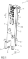
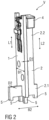
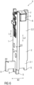
- the figures 1 and 2 and 5 to 7 show schematic representations of a printed circuit board assembly V made up of two printed circuit boards 1, 2 that are connected to one another at least in a form-fitting manner.
- the first printed circuit board 1 carries at least one component 4, in particular an electronic component 4.
- this component 4 is designed as a sensor, so that this first printed circuit board 1 is designed as a sensor carrier printed circuit board.
- the second circuit board 2 is designed as a support circuit board, the function of which is to support the first circuit board 1, in particular during a connection process described below for connecting at least the first circuit board 1 to an in figure 4 illustrated third circuit board 3, for example a main circuit board, to the circuit board assembly V, which then includes these three circuit boards 1, 2, 3.
- This connection process during which the second printed circuit board 2 supports the first printed circuit board 1, so that in particular it is ensured that the first printed circuit board 1 does not change its position relative to the third printed circuit board 3, includes, for example, an assembly process, a soldering process and/or a plastic encapsulation process, in particular with a thermoset plastic.
- the second circuit board 2 one or more components 4, in particular carry electronic components 4 and/or electrical conductor tracks, as does the first printed circuit board 1.
- the printed circuit board assembly V can be used, for example, in a vehicle, for example in a control unit of the vehicle, for example in a transmission control unit.
- a control unit of the vehicle for example in a transmission control unit.
- other possible uses are also conceivable, in particular in electrical or electronic devices which have a plurality of printed circuit boards connected to one another.
- the printed circuit board assembly V which comprises at least the first printed circuit board 1 and the second printed circuit board 2 and expediently also, as in figure 4 shown, also includes the third printed circuit board 3, the first printed circuit board 1 and the second printed circuit board 2 are at least positively connected to one another. This is advantageously done using what is known as a two-groove connection.
- the first printed circuit board 1 and the second printed circuit board 2 each have at least one groove N1, N2.
- the first printed circuit board 1 and the second printed circuit board 2 are, as in figure 3 shown connected to each other in such a way that the bottoms of the two grooves N1, N2 touch.
- the connection of the first printed circuit board 1 and the second printed circuit board 2 is in figure 3 using the example in the figures 1 and 2 shown first circuit board 1 and second circuit board 2 shown. Joining the in the Figures 5 to 7 illustrated embodiments of the first and second printed circuit board 1, 2 is essentially in the same way.
- the first printed circuit board 1 and the second printed circuit board 2 are plate-shaped and therefore each have two opposite flat sides, two longitudinal sides and two transverse sides. The long sides and transverse sides essentially form a peripheral side edge of the respective printed circuit board 1, 2.
- the first printed circuit board 1 and the second printed circuit board 2 are essentially elongated, ie they each have a length dimension L1, L2, a width dimension B1, B2 and a Thickness dimension D1, D2, wherein the length dimension L1, L2 is larger, in particular significantly larger, than the width dimension B1, B2 and wherein the width dimension B1, B2 is larger, in particular significantly larger, than the thickness dimension D1, D2.
- the long sides are longer than the short sides of the respective printed circuit board 1, 2.
- Longitudinal extension L1, L2 means an extension of the respective printed circuit board 1, 2 in its longitudinal direction.
- the width extension B1, B2 is to be understood as meaning an extension of the respective printed circuit board 1, 2 in its transverse direction, ie width direction.
- Thickness expansion D1, D2 is to be understood as meaning an expansion of the respective printed circuit board 1, 2 in its thickness direction.
- the respective groove N1, N2 is designed as a depression in the respective side edge.
- a groove depth direction thus runs from an upper edge of the groove, i. H. from a slot opening to the slot bottom of the respective slot N1, N2.
- a groove direction of the respective groove N1, N2 runs at right angles to the groove depth direction and thus from one flat side to the opposite flat side of the respective printed circuit board 1, 2.
- the groove N1 in the first printed circuit board 1 is formed in the area of one of the transverse sides, with the direction of the groove depth extending in the direction of the other transverse side, i.e. in the direction of the longitudinal extent L1 of the first printed circuit board 1.
- the groove N1 is formed in the region of the transverse side facing away from the component 4 arranged on the first printed circuit board 1. This lateral side, in which the groove N1 is formed, is provided for connection to the third printed circuit board 3.
- the second circuit board 2 has in the embodiments according to Figures 1 to 4 6 and 7 has a wide area 2.1 and an adjoining narrow area 2.2, with a width extension B2 of the wide area 2.1 being greater than a width extension B2 of the narrow area 2.2.
- the wide area 2.1 extends to a transverse side of the second printed circuit board 2, which is provided for connection to the third printed circuit board 3.
- support feet can be provided which are placed on a flat side of the third circuit board 3 .
- the groove N2 is formed in the second circuit board 2 in an edge side of the wide area 2.1, which faces the transverse side of the second circuit board 2 associated with the narrow area 2.2.
- the direction of the groove depth runs in the direction of the length L2 of the second circuit board 2, with the groove bottom being arranged closer to the transverse side associated with the wide area 2.1 and the groove edge consequently being arranged closer to the transverse side associated with the narrow area 2.2.
- One of the groove walls is designed as an extension of a longitudinal edge area of the narrow area 2.2 into the wide area 2.1.
- the side walls of the slot N1 in the first printed circuit board 1 lie on one flat side of the second printed circuit board 2 and the side walls of the slot N2 in the second printed circuit board 2 lie on one flat side of the first one Printed circuit board 1, so that the printed circuit boards 1, 2 are conveniently clamped together via the grooves N1, N2.
- the narrow area 2.2 of the second printed circuit board 2 rests against one flat side of the first printed circuit board 1 over a significant part of the length L1 of the first printed circuit board 1, in particular over more than half of the length L1 of the first printed circuit board 1, and thus supports the first printed circuit board 1, in particular against tilting.
- the first printed circuit board 1 and the second printed circuit board 1 are thus connected to one another or are connected to one another in the finished printed circuit board assembly V in such a way that flat sides of the first printed circuit board 1 are aligned at right angles to flat sides of the second printed circuit board 2, i. H. Surface normals of the first and second printed circuit board 1, 2 are aligned at right angles to one another.
- the length extensions L1, L2, in particular their respective direction, of the two printed circuit boards 1, 2 are aligned parallel to one another.
- the groove extension directions of the two grooves N1, N2 are aligned at right angles to one another and the groove depth directions of the two grooves N1, N2 are aligned parallel to one another.
- Corresponding shaping of the second printed circuit board 2 also makes it possible for at least one component 4, in particular the sensor, to be supported on the first printed circuit board 1 by the second printed circuit board 2, in order thereby to achieve improved positioning accuracy of this component 4.
- this is achieved in that the length dimension L2 of the second printed circuit board 2 is designed in such a way that the second printed circuit board 2 when assembled with the first printed circuit board 1 extends up to the component 4 to be supported on the first printed circuit board 1, i.e. rests against the component 4 to be supported.
- the second printed circuit board 2 is designed in such a way that it encloses the component 4 to be supported at least in regions when it is assembled with the first printed circuit board 1 .
- the The second circuit board 2 has a component recess 6 corresponding to a component shape of the component 4 to be supported, in which the component 4 to be supported is arranged after the joining of the first and second circuit boards 1, 2 and is thereby supported by the second circuit board 2 in several directions, in particular from above and below, i.e. in the direction of length extension of the first circuit board 1.
- this enables the position of the component 4, for example the sensor, to be secured in the plastic encapsulation process.
- the second printed circuit board 2 has a latching lug 7 with which it snaps into place on the component 4 .
- a plurality of components 4 can also be supported on the first circuit board 1 by means of the second circuit board 2, given a corresponding shaping of the second circuit board 2 .
- a correspondingly adapted shape of the second printed circuit board 2 enables support for differently designed components 4, for example for different sensor construction concepts.
- the shape of the second printed circuit board 2 must be adapted to the design of the respective component 4 .
- the first circuit board 1 is designed in such a way as already mentioned above Figures 1 to 4 and 6 and 7 described.
- the second printed circuit board 2 is significantly shorter; it essentially only includes the wide area 2.1 of the second printed circuit board 2 according to the other exemplary embodiments.
- the groove N2 is formed here in the area of one long side, with the groove depth direction extending in the direction of the other long side, i.e. in the direction of the width extension B2 of the second circuit board 2.
- the groove N2 is formed in the area of the long side, which is not intended for connection to the third circuit board 3.
- the other long side, which is designed to be connected to the third printed circuit board 3 is, in this embodiment the second printed circuit board 2 has the two positioning formations 5 or feet in the width extent B2 of the second printed circuit board 2 .
- the first and second printed circuit boards 1, 2 are advantageously connected to one another via the two-groove connector, as shown in FIG figure 3 shown, and then the first and second printed circuit boards 1, 2 are connected to the third printed circuit board 3, as in FIG figure 4 shown.
- the first printed circuit board 1 is held in position on the third printed circuit board 3 by its positioning formations 5, i.e. the positioning pins, expediently in the area of soldering points on the third printed circuit board 3. This positioning is carried out here by clamping the positioning formations 5 in the respective corresponding recess in the third printed circuit board 3.
- the second printed circuit board 2 can first be arranged on the third printed circuit board 3 and then the first printed circuit board 1 in the manner described in the second printed circuit board 2, if present, with its respective positioning formation 5 are inserted into the respective corresponding recess in the third printed circuit board 3.
- the positioning formations 5 of the first and/or second printed circuit board 1, 2 can be metallically coated at least in certain areas, advantageously circumferentially, and soldered into the third printed circuit board 3, expediently without electrical contacting. This is called the principle of blind contact soldering. This soldering of the first and/or second printed circuit board 1, 2 to the third printed circuit board 3 thus only serves to secure the position of the first and/or second printed circuit board 1, 2 relative to the third printed circuit board 3.
- the first printed circuit board 1 is arranged vertically on the second printed circuit board 3, with its length extension L1 parallel to a normal vector of the third printed circuit board 3, i.e. to the normal vector of the flat side of the third printed circuit board 3.
- the component 4 for example the sensor, is arranged on the first printed circuit board 1 at a distance from the third printed circuit board.
- the first printed circuit board 1 is populated after, d. H. after connection to the third printed circuit board 3 in the manner described above and/or after the first and/or third printed circuit board 1, 3 has been fitted with further components 4, in a plastic overmolding tool, in particular in a duroplastic injection molding tool. It is there expediently in the x-direction, i. H. in the direction of thickness extension, and in the y-direction, i. H. in the direction of width expansion, held in the plastic overmoulding tool. The z-direction, i. H. the direction of linear expansion, is expediently left free, d. H. in this direction, the first circuit board 1 is not in contact with an inside of the plastic encapsulation tool, so that no compressive forces act on the third circuit board 3 and soldering points.
- the first printed circuit board 1 is now overmolded with a plastic, in particular with a thermosetting plastic, at least in certain areas or completely.
- the second printed circuit board 2 is also encapsulated in areas or completely and/or at least areas of the third printed circuit board 3 are overmoulded with the plastic, in particular duroplast.
- the component 4 is designed as a sensor on the first printed circuit board 1, a so-called sensor dome is realized by this printed circuit board assembly V.
- the sensor is arranged at a distance from the third printed circuit board 3, which is expediently designed as the main printed circuit board that it can protrude, for example, from a control unit housing and into another unit, for example into a transmission of a vehicle, protrudes or is at least arranged on a housing or in a housing recess of the housing of the other unit.
- the first printed circuit board 1 and the second printed circuit board 2 expediently have one or more corresponding latching formations.
- the first printed circuit board 1 and the second printed circuit board 2 expediently have one or more corresponding latching formations.
- a corresponding printed circuit board latching lug 8 is formed, which snaps into place in the latching opening when the two printed circuit boards 1, 2 are joined together.
- corresponding snap-in hooks can be provided on the first and second printed circuit boards 1, 2, which are pushed into one another and snap into place when the first and second printed circuit boards 1, 2 are joined together. This latching achieves greater stability during the plastic encapsulation and, for example, also during use of the circuit board assembly V.
- support geometries can also be provided on one or more of the printed circuit boards 1, 2, 3, in particular on the first and/or second printed circuit board 1, 2, and/or in the plastic injection molding tool. i.e. appropriate support and/or mount formations.
- the printed circuit board assembly V produced in the manner described thus includes, as shown in FIG figures 1 and 2 5 to 7, at least the first printed circuit board 1 and the second printed circuit board 2, which are connected in the manner described, in particular by two-groove plugging, at least in a form-fitting manner, for example also in a force-fitting manner.
- the printed circuit board assembly V produced in the manner described expediently comprises the first, second and third printed circuit boards 1, 2, 3, with at least the first printed circuit board 1 and the second printed circuit board 2 being connected in the manner described, in particular by means of a two-groove connection, at least in a form-fitting manner, for example also in a force-fitting manner.
- the first and/or second printed circuit board 1, 2 are connected to the third printed circuit board 3, for example, in a form-fitting, force-fitting and/or cohesive manner, cohesively in particular through the plastic, in particular duroplastic, due to the plastic encapsulation described above, and/or, for example, by soldering.
- the positive connection of the first and/or second printed circuit board 1, 2 to the third printed circuit board 3 is achieved, for example, by one or more positioning formations 5 introduced into respective recesses in the third printed circuit board 3.
- the form fit between the first and second circuit board 1, 2 can also result from the latching described above.
- the printed circuit board assembly V can be used, for example, in a transmission control unit for a vehicle or in another control unit or in another electrical device.
- the first printed circuit board 1 is expediently designed as a sensor carrier printed circuit board and carries the sensor as a component 4 .
- the second printed circuit board 2 is designed as a support printed circuit board and the third printed circuit board 3 as a main printed circuit board.
- the arrangement of the first printed circuit board 1 supported by the second printed circuit board 2 on the third printed circuit board 3 forms a so-called sensor dome.
Landscapes
- Engineering & Computer Science (AREA)
- Microelectronics & Electronic Packaging (AREA)
- Manufacturing & Machinery (AREA)
- Combinations Of Printed Boards (AREA)
- Structure Of Printed Boards (AREA)
Claims (7)
- Procédé de fabrication d'un assemblage de cartes de circuits imprimés (V), une première carte de circuits imprimés (1), notamment une carte de circuits imprimés porte-capteur, étant reliée par complémentarité de formes à une deuxième carte de circuits imprimés (2), notamment une carte de circuits imprimés de soutien, les extensions longitudinales (L1, L2) des deux cartes de circuits imprimés (1, 2) étant orientées parallèlement l'une à l'autre, les deux cartes de circuits imprimés (1, 2) présentant chacune une rainure (N1, N2) et les deux cartes de circuits imprimés (1, 2) étant reliées l'une à l'autre de telle sorte que les fonds de rainure des deux rainures (N1, N2) se touchent, les deux cartes de circuits imprimés (1, 2) étant reliées en étant orientées l'une par rapport à l'autre de telle sorte que les normales aux surfaces des deux cartes de circuits imprimés (1, 2) sont orientées à angle droit l'une de l'autre,
caractérisé en ce quela rainure (N1) est formée dans la zone du côté transversal détourné d'un composant (4) agencé sur la première carte de circuits imprimés (1),la deuxième carte de circuits imprimés (2) présente une zone large (2.1) et une zone étroite (2.2) qui s'y raccorde, la zone étroite (2.2) étant située sur une partie essentielle de l'extension longitudinale (L1) de la première carte de circuits imprimés (1), et la rainure (N2) dans la deuxième carte de circuits imprimés (2) étant formée dans un côté de bord de la zone large (2.1), et en ce queles cartes de circuits imprimés (1, 2) sont reliées entre elles de telle sorte que le composant (4), notamment le capteur, agencé sur la première carte de circuits imprimés (1) est soutenu dans sa position par la deuxième carte de circuits imprimés (2). - Procédé selon la revendication 1,
dans lequel les deux cartes de circuits imprimés (1, 2) sont encliquetées l'une avec l'autre. - Procédé selon l'une quelconque des revendications précédentes,
dans lequel au moins la première carte de circuits imprimés (1) est reliée à une troisième carte de circuits imprimés (3). - Procédé selon l'une quelconque des revendications précédentes,
dans lequel au moins une formation de positionnement (5) de la première carte de circuits imprimés (1) est insérée dans un évidement correspondant de la troisième carte de circuits imprimés (3) et/ou la première carte de circuits imprimés (1) et la troisième carte de circuits imprimés (3) sont soudées ensemble. - Procédé selon l'une quelconque des revendications précédentes,
dans lequel au moins la première carte de circuits imprimés (1) est surmoulée avec une matière plastique au moins par zones. - Assemblage de cartes de circuits imprimés (V), notamment fabriqué au moyen d'un procédé selon l'une quelconque des revendications précédentes, comprenant au moins deux cartes de circuits imprimés (1, 2) reliées entre elles par complémentarité de forme, une première carte de circuits imprimés (1), notamment une carte de circuits imprimés porte-capteur, étant reliée par complémentarité de formes à une deuxième carte de circuits imprimés (2), notamment une carte de circuits imprimés de soutien, les extensions longitudinales (L1, L2) des deux cartes de circuits imprimés (1, 2) étant orientées parallèlement l'une à l'autre, les deux cartes de circuits imprimés (1, 2) présentant chacune une rainure (N1, N2) et les deux cartes de circuits imprimés (1, 2) étant reliées l'une à l'autre de telle sorte que les fonds de rainure des deux rainures (N1, N2) se touchent, les deux cartes de circuits imprimés (1, 2) étant reliées en étant orientées l'une par rapport à l'autre de telle sorte que les normales aux surfaces des deux cartes de circuits imprimés (1, 2) sont orientées à angle droit l'une de l'autre,
caractérisé en ce que
la rainure (N1) est formée dans la zone du côté transversal détourné d'un composant (4) agencé sur la première carte de circuits imprimés (1), la deuxième carte de circuits imprimés (2) présente une zone large (2.1) et une zone étroite (2.2) qui s'y raccorde, la zone étroite (2.2) étant située sur une partie essentielle de l'extension longitudinale (L1) de la première carte de circuits imprimés (1), et la rainure (N2) dans la deuxième carte de circuits imprimés (2) étant formée dans un côté de bord de la zone large (2.1), et en ce que les cartes de circuits imprimés (1, 2) sont reliées entre elles de telle sorte que le composant (4), notamment le capteur, agencé sur la première carte de circuits imprimés (1) est soutenu dans sa position par la deuxième carte de circuits imprimés (2). - Assemblage de cartes de circuits imprimés (V) selon la revendication 6, comprenant trois cartes de circuits imprimés (1, 2, 3) reliées entre elles.
Applications Claiming Priority (2)
| Application Number | Priority Date | Filing Date | Title |
|---|---|---|---|
| DE102016224653.4A DE102016224653B4 (de) | 2016-12-12 | 2016-12-12 | Leiterplattenverbund und Verfahren zu dessen Herstellung |
| PCT/EP2017/082109 WO2018108758A1 (fr) | 2016-12-12 | 2017-12-08 | Assemblage de cartes de circuits imprimés et son procédé de fabrication |
Publications (2)
| Publication Number | Publication Date |
|---|---|
| EP3552463A1 EP3552463A1 (fr) | 2019-10-16 |
| EP3552463B1 true EP3552463B1 (fr) | 2023-07-26 |
Family
ID=60702710
Family Applications (1)
| Application Number | Title | Priority Date | Filing Date |
|---|---|---|---|
| EP17816673.2A Active EP3552463B1 (fr) | 2016-12-12 | 2017-12-08 | Assemblage de cartes de circuits imprimés et son procédé de fabrication |
Country Status (7)
| Country | Link |
|---|---|
| US (1) | US10893615B2 (fr) |
| EP (1) | EP3552463B1 (fr) |
| JP (1) | JP6828164B2 (fr) |
| KR (1) | KR102423939B1 (fr) |
| CN (1) | CN110169212B (fr) |
| DE (1) | DE102016224653B4 (fr) |
| WO (1) | WO2018108758A1 (fr) |
Families Citing this family (7)
| Publication number | Priority date | Publication date | Assignee | Title |
|---|---|---|---|---|
| KR102622914B1 (ko) * | 2017-02-06 | 2024-01-10 | 삼성전자주식회사 | 전력 공급 장치 및 전력 공급 장치를 포함하는 전자 장치 |
| JP1663818S (fr) * | 2018-12-26 | 2020-07-20 | ||
| USD936025S1 (en) * | 2018-12-26 | 2021-11-16 | Lg Chem, Ltd. | Flexible printed circuit board for battery module |
| TWD202895S (zh) * | 2019-03-27 | 2020-02-21 | 家登精密工業股份有限公司 | 光罩盒組裝件 |
| CN114498117B (zh) * | 2020-10-23 | 2024-06-18 | 台达电子工业股份有限公司 | 插座结构 |
| EP4509411A1 (fr) | 2023-08-16 | 2025-02-19 | Goodrich Lighting Systems GmbH & Co. KG | Feu d'aéronef, aéronef comprenant un feu d'aéronef et procédé d'assemblage d'un feu d'aéronef |
| DE102024200130B3 (de) | 2024-01-05 | 2025-03-20 | Vitesco Technologies Germany Gmbh | Elektronikbaugruppe und Verfahren zur Herstellung der Elektronikbaugruppe |
Family Cites Families (24)
| Publication number | Priority date | Publication date | Assignee | Title |
|---|---|---|---|---|
| US2958013A (en) * | 1956-08-20 | 1960-10-25 | Arthur Ansley Mfg Co | Electrical unit |
| US3522485A (en) * | 1967-11-21 | 1970-08-04 | Automatic Radio Mfg Co | Modular circuit construction |
| DE2441209A1 (de) | 1974-08-28 | 1976-03-11 | Erie Elektronik Gmbh | Elektrische anschlusskontaktierung |
| US4513064A (en) * | 1982-12-17 | 1985-04-23 | The United States Of America As Represented By The Secretary Of The Army | Package for rugged electronics |
| JPS6251769U (fr) * | 1985-09-18 | 1987-03-31 | ||
| DE3919273C2 (de) | 1989-06-13 | 1993-10-14 | Bosch Gmbh Robert | Leiterplattenanordnung |
| DE4244626C2 (de) * | 1992-12-29 | 1995-02-09 | Mannesmann Ag | Anordnung zum Positionieren |
| JPH1154875A (ja) * | 1997-07-31 | 1999-02-26 | Nec Home Electron Ltd | プリント基板の保持構造 |
| US20020071259A1 (en) | 2000-11-13 | 2002-06-13 | Sture Roos | Circuit board assembly |
| SE0004161D0 (sv) * | 2000-11-13 | 2000-11-13 | Ericsson Telefon Ab L M | Circuit board assembly |
| US6804120B2 (en) * | 2001-12-18 | 2004-10-12 | Siemens Vdo Automotive Corporation | Method and apparatus for connecting circuit boards for a sensor assembly |
| JP2008071848A (ja) * | 2006-09-13 | 2008-03-27 | Funai Electric Co Ltd | テレビジョン受像機用回路基板ユニット及び電子機器用回路基板ユニット |
| US7435095B1 (en) * | 2007-06-11 | 2008-10-14 | Hon Hai Precision Ind. Co., Ltd. | Electrical interconnection system |
| US7864544B2 (en) * | 2007-08-01 | 2011-01-04 | Delphi Technologies, Inc. | Printed circuit board assembly |
| JP2009152331A (ja) * | 2007-12-20 | 2009-07-09 | Panasonic Corp | 配線基板の加工方法、および半導体装置 |
| US8328571B2 (en) * | 2010-11-04 | 2012-12-11 | Tyco Electronics Corporation | Connector assemblies having moveable mating arrays and power connectors |
| CH704882A2 (fr) * | 2011-04-29 | 2012-10-31 | Fischer Connectors Holding Sa | Connecteur haute densité. |
| CN102858088A (zh) | 2011-06-28 | 2013-01-02 | 鸿富锦精密工业(深圳)有限公司 | 电路板及其制作方法及采用该电路板的电子产品 |
| GB2494919B (en) * | 2011-09-23 | 2015-06-17 | Control Tech Ltd | Method for connecting printed circuit boards. |
| TWI456379B (zh) * | 2012-07-23 | 2014-10-11 | Chicony Power Tech Co Ltd | 電源系統及其組合式電源裝置 |
| DE102012213304A1 (de) * | 2012-07-30 | 2014-01-30 | Zf Friedrichshafen Ag | Verfahren zum Herstellen einer dreidimensionalen Leiterplattenanordnung und dreidimensionale Leiterplattenanordnung |
| US9163792B2 (en) | 2013-07-23 | 2015-10-20 | Zacaabel, Llc | Illuminated hand wand |
| US9108262B1 (en) * | 2014-04-17 | 2015-08-18 | Topline Corporation | Disposable apparatus for aligning and dispensing solder columns in an array |
| DE102016224657A1 (de) * | 2016-12-12 | 2018-06-14 | Conti Temic Microelectronic Gmbh | Verfahren zum Verbinden eines Bauelementträgers mit einer Leiterplatte und Verbund aus einer Leiterplatte und einem Bauelementträger |
-
2016
- 2016-12-12 DE DE102016224653.4A patent/DE102016224653B4/de not_active Expired - Fee Related
-
2017
- 2017-12-08 KR KR1020197018382A patent/KR102423939B1/ko active Active
- 2017-12-08 EP EP17816673.2A patent/EP3552463B1/fr active Active
- 2017-12-08 US US16/468,820 patent/US10893615B2/en active Active
- 2017-12-08 JP JP2019531276A patent/JP6828164B2/ja active Active
- 2017-12-08 CN CN201780071642.2A patent/CN110169212B/zh active Active
- 2017-12-08 WO PCT/EP2017/082109 patent/WO2018108758A1/fr not_active Ceased
Also Published As
| Publication number | Publication date |
|---|---|
| JP2020501377A (ja) | 2020-01-16 |
| KR20190087565A (ko) | 2019-07-24 |
| DE102016224653B4 (de) | 2022-07-21 |
| US20200077525A1 (en) | 2020-03-05 |
| WO2018108758A1 (fr) | 2018-06-21 |
| DE102016224653A1 (de) | 2018-06-14 |
| KR102423939B1 (ko) | 2022-07-21 |
| CN110169212B (zh) | 2023-01-20 |
| CN110169212A (zh) | 2019-08-23 |
| EP3552463A1 (fr) | 2019-10-16 |
| US10893615B2 (en) | 2021-01-12 |
| JP6828164B2 (ja) | 2021-02-10 |
Similar Documents
| Publication | Publication Date | Title |
|---|---|---|
| EP3552463B1 (fr) | Assemblage de cartes de circuits imprimés et son procédé de fabrication | |
| DE69816882T2 (de) | Verfahren zum Herstellen eines Verbinders und ein Verbinder hergestellt durch Formen mit Einsetzung und dessen Verwendung | |
| DE112017007139B4 (de) | Gehäuse, elektronische Vorrichtung und Verfahren zur Herstellung eines Gehäuses | |
| EP0982978B1 (fr) | Boítier, en particulier boítier de serrure avec interconnections électriques | |
| WO2013178212A2 (fr) | Support pour composant de véhicule à moteur et procédé de fabrication dudit support | |
| DE102013209435A1 (de) | Steckerverbindung mit einem zur Vermeidung von Spänen optimierten Führungselement | |
| DE10260241B4 (de) | Kontaktierungsbauteil und Verfahren zur Herstellung eines Kontaktierungsbauteils | |
| DE102010034975A1 (de) | Elektronische Schaltung | |
| DE102016119057B4 (de) | Sensorelement für einen kapazitiven Sensor und Verfahren zur Herstellung des Sensorelements und des Sensors | |
| DE102012105352A1 (de) | Positionierelement | |
| DE102014216518A1 (de) | Elektronische Steuereinheit sowie Moldwerkzeug und Verfahren zum Herstellen einer elektronischen Steuereinheit | |
| DE102005039086B4 (de) | Verfahren zum Herstellen einer elektrischen Verbindungseinrichtung sowie derart hergestellte Verbindungseinrichtung | |
| DE10345632B4 (de) | Anordnung mit einem Sensor | |
| DE102018206480B4 (de) | Verbinder und Steuergerät | |
| DE102016224657A1 (de) | Verfahren zum Verbinden eines Bauelementträgers mit einer Leiterplatte und Verbund aus einer Leiterplatte und einem Bauelementträger | |
| DE102017011113B4 (de) | Elektrisches Verbindungselement mit einer Stromschiene | |
| DE102014204051A1 (de) | Verbindungsanordnung, Verfahren zum Herstellen einer Verbindungsanordnung und elektrisches Gerät mit einer Verbindungsanordnung | |
| WO2019038285A1 (fr) | Composant de capteur, ensemble de prémontage pour un composant de capteur et procédé de fabrication d'un composant de capteur | |
| LU101641B1 (de) | System aus einem Steckkontaktträger und wenigstens einem Steckkontaktelement , Steckkontaktträger, Steckkontaktelement und Steckverbinder | |
| DE10306618A1 (de) | Planare Kontaktstruktur mit Kontaktzungen für eine variable Steckposition | |
| DE102007002749B3 (de) | Modularer Steckeraufbau | |
| DE102023201588A1 (de) | Elektronikmodul | |
| DE19841467A1 (de) | Platinen-Steckkontakt-Anordnung | |
| DE102024113214A1 (de) | Kontaktelement und Steckverbinder | |
| DE102016219662A1 (de) | Gehäuse zur Aufnahme einer ein- oder mehrteiligen Leiterplatte |
Legal Events
| Date | Code | Title | Description |
|---|---|---|---|
| STAA | Information on the status of an ep patent application or granted ep patent |
Free format text: STATUS: UNKNOWN |
|
| STAA | Information on the status of an ep patent application or granted ep patent |
Free format text: STATUS: THE INTERNATIONAL PUBLICATION HAS BEEN MADE |
|
| PUAI | Public reference made under article 153(3) epc to a published international application that has entered the european phase |
Free format text: ORIGINAL CODE: 0009012 |
|
| STAA | Information on the status of an ep patent application or granted ep patent |
Free format text: STATUS: REQUEST FOR EXAMINATION WAS MADE |
|
| 17P | Request for examination filed |
Effective date: 20190524 |
|
| AK | Designated contracting states |
Kind code of ref document: A1 Designated state(s): AL AT BE BG CH CY CZ DE DK EE ES FI FR GB GR HR HU IE IS IT LI LT LU LV MC MK MT NL NO PL PT RO RS SE SI SK SM TR |
|
| AX | Request for extension of the european patent |
Extension state: BA ME |
|
| RAP1 | Party data changed (applicant data changed or rights of an application transferred) |
Owner name: VITESCO TECHNOLOGIES GERMANY GMBH |
|
| DAV | Request for validation of the european patent (deleted) | ||
| DAX | Request for extension of the european patent (deleted) | ||
| STAA | Information on the status of an ep patent application or granted ep patent |
Free format text: STATUS: EXAMINATION IS IN PROGRESS |
|
| 17Q | First examination report despatched |
Effective date: 20210407 |
|
| RAP3 | Party data changed (applicant data changed or rights of an application transferred) |
Owner name: VITESCO TECHNOLOGIES GERMANY GMBH |
|
| GRAP | Despatch of communication of intention to grant a patent |
Free format text: ORIGINAL CODE: EPIDOSNIGR1 |
|
| STAA | Information on the status of an ep patent application or granted ep patent |
Free format text: STATUS: GRANT OF PATENT IS INTENDED |
|
| INTG | Intention to grant announced |
Effective date: 20230329 |
|
| GRAS | Grant fee paid |
Free format text: ORIGINAL CODE: EPIDOSNIGR3 |
|
| GRAA | (expected) grant |
Free format text: ORIGINAL CODE: 0009210 |
|
| STAA | Information on the status of an ep patent application or granted ep patent |
Free format text: STATUS: THE PATENT HAS BEEN GRANTED |
|
| P01 | Opt-out of the competence of the unified patent court (upc) registered |
Effective date: 20230530 |
|
| AK | Designated contracting states |
Kind code of ref document: B1 Designated state(s): AL AT BE BG CH CY CZ DE DK EE ES FI FR GB GR HR HU IE IS IT LI LT LU LV MC MK MT NL NO PL PT RO RS SE SI SK SM TR |
|
| REG | Reference to a national code |
Ref country code: CH Ref legal event code: EP |
|
| REG | Reference to a national code |
Ref country code: DE Ref legal event code: R096 Ref document number: 502017015118 Country of ref document: DE |
|
| REG | Reference to a national code |
Ref country code: IE Ref legal event code: FG4D Free format text: LANGUAGE OF EP DOCUMENT: GERMAN |
|
| REG | Reference to a national code |
Ref country code: LT Ref legal event code: MG9D |
|
| REG | Reference to a national code |
Ref country code: NL Ref legal event code: MP Effective date: 20230726 |
|
| PG25 | Lapsed in a contracting state [announced via postgrant information from national office to epo] |
Ref country code: NL Free format text: LAPSE BECAUSE OF FAILURE TO SUBMIT A TRANSLATION OF THE DESCRIPTION OR TO PAY THE FEE WITHIN THE PRESCRIBED TIME-LIMIT Effective date: 20230726 |
|
| PG25 | Lapsed in a contracting state [announced via postgrant information from national office to epo] |
Ref country code: GR Free format text: LAPSE BECAUSE OF FAILURE TO SUBMIT A TRANSLATION OF THE DESCRIPTION OR TO PAY THE FEE WITHIN THE PRESCRIBED TIME-LIMIT Effective date: 20231027 |
|
| PG25 | Lapsed in a contracting state [announced via postgrant information from national office to epo] |
Ref country code: IS Free format text: LAPSE BECAUSE OF FAILURE TO SUBMIT A TRANSLATION OF THE DESCRIPTION OR TO PAY THE FEE WITHIN THE PRESCRIBED TIME-LIMIT Effective date: 20231126 |
|
| PG25 | Lapsed in a contracting state [announced via postgrant information from national office to epo] |
Ref country code: SE Free format text: LAPSE BECAUSE OF FAILURE TO SUBMIT A TRANSLATION OF THE DESCRIPTION OR TO PAY THE FEE WITHIN THE PRESCRIBED TIME-LIMIT Effective date: 20230726 Ref country code: RS Free format text: LAPSE BECAUSE OF FAILURE TO SUBMIT A TRANSLATION OF THE DESCRIPTION OR TO PAY THE FEE WITHIN THE PRESCRIBED TIME-LIMIT Effective date: 20230726 Ref country code: PT Free format text: LAPSE BECAUSE OF FAILURE TO SUBMIT A TRANSLATION OF THE DESCRIPTION OR TO PAY THE FEE WITHIN THE PRESCRIBED TIME-LIMIT Effective date: 20231127 Ref country code: NO Free format text: LAPSE BECAUSE OF FAILURE TO SUBMIT A TRANSLATION OF THE DESCRIPTION OR TO PAY THE FEE WITHIN THE PRESCRIBED TIME-LIMIT Effective date: 20231026 Ref country code: LV Free format text: LAPSE BECAUSE OF FAILURE TO SUBMIT A TRANSLATION OF THE DESCRIPTION OR TO PAY THE FEE WITHIN THE PRESCRIBED TIME-LIMIT Effective date: 20230726 Ref country code: LT Free format text: LAPSE BECAUSE OF FAILURE TO SUBMIT A TRANSLATION OF THE DESCRIPTION OR TO PAY THE FEE WITHIN THE PRESCRIBED TIME-LIMIT Effective date: 20230726 Ref country code: IS Free format text: LAPSE BECAUSE OF FAILURE TO SUBMIT A TRANSLATION OF THE DESCRIPTION OR TO PAY THE FEE WITHIN THE PRESCRIBED TIME-LIMIT Effective date: 20231126 Ref country code: HR Free format text: LAPSE BECAUSE OF FAILURE TO SUBMIT A TRANSLATION OF THE DESCRIPTION OR TO PAY THE FEE WITHIN THE PRESCRIBED TIME-LIMIT Effective date: 20230726 Ref country code: GR Free format text: LAPSE BECAUSE OF FAILURE TO SUBMIT A TRANSLATION OF THE DESCRIPTION OR TO PAY THE FEE WITHIN THE PRESCRIBED TIME-LIMIT Effective date: 20231027 Ref country code: FI Free format text: LAPSE BECAUSE OF FAILURE TO SUBMIT A TRANSLATION OF THE DESCRIPTION OR TO PAY THE FEE WITHIN THE PRESCRIBED TIME-LIMIT Effective date: 20230726 |
|
| PG25 | Lapsed in a contracting state [announced via postgrant information from national office to epo] |
Ref country code: PL Free format text: LAPSE BECAUSE OF FAILURE TO SUBMIT A TRANSLATION OF THE DESCRIPTION OR TO PAY THE FEE WITHIN THE PRESCRIBED TIME-LIMIT Effective date: 20230726 |
|
| PG25 | Lapsed in a contracting state [announced via postgrant information from national office to epo] |
Ref country code: ES Free format text: LAPSE BECAUSE OF FAILURE TO SUBMIT A TRANSLATION OF THE DESCRIPTION OR TO PAY THE FEE WITHIN THE PRESCRIBED TIME-LIMIT Effective date: 20230726 |
|
| REG | Reference to a national code |
Ref country code: DE Ref legal event code: R097 Ref document number: 502017015118 Country of ref document: DE |
|
| PG25 | Lapsed in a contracting state [announced via postgrant information from national office to epo] |
Ref country code: SM Free format text: LAPSE BECAUSE OF FAILURE TO SUBMIT A TRANSLATION OF THE DESCRIPTION OR TO PAY THE FEE WITHIN THE PRESCRIBED TIME-LIMIT Effective date: 20230726 Ref country code: RO Free format text: LAPSE BECAUSE OF FAILURE TO SUBMIT A TRANSLATION OF THE DESCRIPTION OR TO PAY THE FEE WITHIN THE PRESCRIBED TIME-LIMIT Effective date: 20230726 Ref country code: ES Free format text: LAPSE BECAUSE OF FAILURE TO SUBMIT A TRANSLATION OF THE DESCRIPTION OR TO PAY THE FEE WITHIN THE PRESCRIBED TIME-LIMIT Effective date: 20230726 Ref country code: EE Free format text: LAPSE BECAUSE OF FAILURE TO SUBMIT A TRANSLATION OF THE DESCRIPTION OR TO PAY THE FEE WITHIN THE PRESCRIBED TIME-LIMIT Effective date: 20230726 Ref country code: DK Free format text: LAPSE BECAUSE OF FAILURE TO SUBMIT A TRANSLATION OF THE DESCRIPTION OR TO PAY THE FEE WITHIN THE PRESCRIBED TIME-LIMIT Effective date: 20230726 Ref country code: CZ Free format text: LAPSE BECAUSE OF FAILURE TO SUBMIT A TRANSLATION OF THE DESCRIPTION OR TO PAY THE FEE WITHIN THE PRESCRIBED TIME-LIMIT Effective date: 20230726 Ref country code: SK Free format text: LAPSE BECAUSE OF FAILURE TO SUBMIT A TRANSLATION OF THE DESCRIPTION OR TO PAY THE FEE WITHIN THE PRESCRIBED TIME-LIMIT Effective date: 20230726 |
|
| PG25 | Lapsed in a contracting state [announced via postgrant information from national office to epo] |
Ref country code: IT Free format text: LAPSE BECAUSE OF FAILURE TO SUBMIT A TRANSLATION OF THE DESCRIPTION OR TO PAY THE FEE WITHIN THE PRESCRIBED TIME-LIMIT Effective date: 20230726 |
|
| PLBE | No opposition filed within time limit |
Free format text: ORIGINAL CODE: 0009261 |
|
| STAA | Information on the status of an ep patent application or granted ep patent |
Free format text: STATUS: NO OPPOSITION FILED WITHIN TIME LIMIT |
|
| 26N | No opposition filed |
Effective date: 20240429 |
|
| PG25 | Lapsed in a contracting state [announced via postgrant information from national office to epo] |
Ref country code: SI Free format text: LAPSE BECAUSE OF FAILURE TO SUBMIT A TRANSLATION OF THE DESCRIPTION OR TO PAY THE FEE WITHIN THE PRESCRIBED TIME-LIMIT Effective date: 20230726 |
|
| REG | Reference to a national code |
Ref country code: CH Ref legal event code: PL |
|
| PG25 | Lapsed in a contracting state [announced via postgrant information from national office to epo] |
Ref country code: LU Free format text: LAPSE BECAUSE OF NON-PAYMENT OF DUE FEES Effective date: 20231208 |
|
| PG25 | Lapsed in a contracting state [announced via postgrant information from national office to epo] |
Ref country code: MC Free format text: LAPSE BECAUSE OF FAILURE TO SUBMIT A TRANSLATION OF THE DESCRIPTION OR TO PAY THE FEE WITHIN THE PRESCRIBED TIME-LIMIT Effective date: 20230726 |
|
| GBPC | Gb: european patent ceased through non-payment of renewal fee |
Effective date: 20231208 |
|
| REG | Reference to a national code |
Ref country code: BE Ref legal event code: MM Effective date: 20231231 |
|
| PG25 | Lapsed in a contracting state [announced via postgrant information from national office to epo] |
Ref country code: MC Free format text: LAPSE BECAUSE OF FAILURE TO SUBMIT A TRANSLATION OF THE DESCRIPTION OR TO PAY THE FEE WITHIN THE PRESCRIBED TIME-LIMIT Effective date: 20230726 Ref country code: LU Free format text: LAPSE BECAUSE OF NON-PAYMENT OF DUE FEES Effective date: 20231208 |
|
| REG | Reference to a national code |
Ref country code: IE Ref legal event code: MM4A |
|
| PG25 | Lapsed in a contracting state [announced via postgrant information from national office to epo] |
Ref country code: IE Free format text: LAPSE BECAUSE OF NON-PAYMENT OF DUE FEES Effective date: 20231208 |
|
| PG25 | Lapsed in a contracting state [announced via postgrant information from national office to epo] |
Ref country code: GB Free format text: LAPSE BECAUSE OF NON-PAYMENT OF DUE FEES Effective date: 20231208 |
|
| PG25 | Lapsed in a contracting state [announced via postgrant information from national office to epo] |
Ref country code: BE Free format text: LAPSE BECAUSE OF NON-PAYMENT OF DUE FEES Effective date: 20231231 |
|
| PG25 | Lapsed in a contracting state [announced via postgrant information from national office to epo] |
Ref country code: CH Free format text: LAPSE BECAUSE OF NON-PAYMENT OF DUE FEES Effective date: 20231231 |
|
| PG25 | Lapsed in a contracting state [announced via postgrant information from national office to epo] |
Ref country code: IE Free format text: LAPSE BECAUSE OF NON-PAYMENT OF DUE FEES Effective date: 20231208 Ref country code: GB Free format text: LAPSE BECAUSE OF NON-PAYMENT OF DUE FEES Effective date: 20231208 Ref country code: CH Free format text: LAPSE BECAUSE OF NON-PAYMENT OF DUE FEES Effective date: 20231231 Ref country code: BE Free format text: LAPSE BECAUSE OF NON-PAYMENT OF DUE FEES Effective date: 20231231 |
|
| PG25 | Lapsed in a contracting state [announced via postgrant information from national office to epo] |
Ref country code: BG Free format text: LAPSE BECAUSE OF FAILURE TO SUBMIT A TRANSLATION OF THE DESCRIPTION OR TO PAY THE FEE WITHIN THE PRESCRIBED TIME-LIMIT Effective date: 20230726 |
|
| PG25 | Lapsed in a contracting state [announced via postgrant information from national office to epo] |
Ref country code: BG Free format text: LAPSE BECAUSE OF FAILURE TO SUBMIT A TRANSLATION OF THE DESCRIPTION OR TO PAY THE FEE WITHIN THE PRESCRIBED TIME-LIMIT Effective date: 20230726 |
|
| REG | Reference to a national code |
Ref country code: AT Ref legal event code: MM01 Ref document number: 1593476 Country of ref document: AT Kind code of ref document: T Effective date: 20231208 |
|
| REG | Reference to a national code |
Ref country code: DE Ref legal event code: R081 Ref document number: 502017015118 Country of ref document: DE Owner name: SCHAEFFLER TECHNOLOGIES AG & CO. KG, DE Free format text: FORMER OWNER: VITESCO TECHNOLOGIES GERMANY GMBH, REGENSBURG, DE |
|
| PG25 | Lapsed in a contracting state [announced via postgrant information from national office to epo] |
Ref country code: AT Free format text: LAPSE BECAUSE OF NON-PAYMENT OF DUE FEES Effective date: 20231208 |
|
| PG25 | Lapsed in a contracting state [announced via postgrant information from national office to epo] |
Ref country code: CY Free format text: LAPSE BECAUSE OF FAILURE TO SUBMIT A TRANSLATION OF THE DESCRIPTION OR TO PAY THE FEE WITHIN THE PRESCRIBED TIME-LIMIT; INVALID AB INITIO Effective date: 20171208 |
|
| PG25 | Lapsed in a contracting state [announced via postgrant information from national office to epo] |
Ref country code: HU Free format text: LAPSE BECAUSE OF FAILURE TO SUBMIT A TRANSLATION OF THE DESCRIPTION OR TO PAY THE FEE WITHIN THE PRESCRIBED TIME-LIMIT; INVALID AB INITIO Effective date: 20171208 |
|
| PG25 | Lapsed in a contracting state [announced via postgrant information from national office to epo] |
Ref country code: TR Free format text: LAPSE BECAUSE OF FAILURE TO SUBMIT A TRANSLATION OF THE DESCRIPTION OR TO PAY THE FEE WITHIN THE PRESCRIBED TIME-LIMIT Effective date: 20230726 |
|
| PGFP | Annual fee paid to national office [announced via postgrant information from national office to epo] |
Ref country code: FR Payment date: 20251229 Year of fee payment: 9 |
|
| PGFP | Annual fee paid to national office [announced via postgrant information from national office to epo] |
Ref country code: DE Payment date: 20251231 Year of fee payment: 9 |