EP3553832A1 - Module de cellules solaires - Google Patents
Module de cellules solaires Download PDFInfo
- Publication number
- EP3553832A1 EP3553832A1 EP17879377.4A EP17879377A EP3553832A1 EP 3553832 A1 EP3553832 A1 EP 3553832A1 EP 17879377 A EP17879377 A EP 17879377A EP 3553832 A1 EP3553832 A1 EP 3553832A1
- Authority
- EP
- European Patent Office
- Prior art keywords
- solar cell
- wiring member
- light
- cell module
- receiving
- Prior art date
- Legal status (The legal status is an assumption and is not a legal conclusion. Google has not performed a legal analysis and makes no representation as to the accuracy of the status listed.)
- Granted
Links
Images
Classifications
-
- H—ELECTRICITY
- H10—SEMICONDUCTOR DEVICES; ELECTRIC SOLID-STATE DEVICES NOT OTHERWISE PROVIDED FOR
- H10F—INORGANIC SEMICONDUCTOR DEVICES SENSITIVE TO INFRARED RADIATION, LIGHT, ELECTROMAGNETIC RADIATION OF SHORTER WAVELENGTH OR CORPUSCULAR RADIATION
- H10F77/00—Constructional details of devices covered by this subclass
-
- H—ELECTRICITY
- H10—SEMICONDUCTOR DEVICES; ELECTRIC SOLID-STATE DEVICES NOT OTHERWISE PROVIDED FOR
- H10F—INORGANIC SEMICONDUCTOR DEVICES SENSITIVE TO INFRARED RADIATION, LIGHT, ELECTROMAGNETIC RADIATION OF SHORTER WAVELENGTH OR CORPUSCULAR RADIATION
- H10F19/00—Integrated devices, or assemblies of multiple devices, comprising at least one photovoltaic cell covered by group H10F10/00, e.g. photovoltaic modules
- H10F19/80—Encapsulations or containers for integrated devices, or assemblies of multiple devices, having photovoltaic cells
- H10F19/85—Protective back sheets
-
- H—ELECTRICITY
- H10—SEMICONDUCTOR DEVICES; ELECTRIC SOLID-STATE DEVICES NOT OTHERWISE PROVIDED FOR
- H10F—INORGANIC SEMICONDUCTOR DEVICES SENSITIVE TO INFRARED RADIATION, LIGHT, ELECTROMAGNETIC RADIATION OF SHORTER WAVELENGTH OR CORPUSCULAR RADIATION
- H10F19/00—Integrated devices, or assemblies of multiple devices, comprising at least one photovoltaic cell covered by group H10F10/00, e.g. photovoltaic modules
- H10F19/90—Structures for connecting between photovoltaic cells, e.g. interconnections or insulating spacers
- H10F19/902—Structures for connecting between photovoltaic cells, e.g. interconnections or insulating spacers for series or parallel connection of photovoltaic cells
- H10F19/906—Structures for connecting between photovoltaic cells, e.g. interconnections or insulating spacers for series or parallel connection of photovoltaic cells characterised by the materials of the structures
-
- H—ELECTRICITY
- H10—SEMICONDUCTOR DEVICES; ELECTRIC SOLID-STATE DEVICES NOT OTHERWISE PROVIDED FOR
- H10F—INORGANIC SEMICONDUCTOR DEVICES SENSITIVE TO INFRARED RADIATION, LIGHT, ELECTROMAGNETIC RADIATION OF SHORTER WAVELENGTH OR CORPUSCULAR RADIATION
- H10F77/00—Constructional details of devices covered by this subclass
- H10F77/40—Optical elements or arrangements
- H10F77/42—Optical elements or arrangements directly associated or integrated with photovoltaic cells, e.g. light-reflecting means or light-concentrating means
- H10F77/48—Back surface reflectors [BSR]
-
- H—ELECTRICITY
- H10—SEMICONDUCTOR DEVICES; ELECTRIC SOLID-STATE DEVICES NOT OTHERWISE PROVIDED FOR
- H10F—INORGANIC SEMICONDUCTOR DEVICES SENSITIVE TO INFRARED RADIATION, LIGHT, ELECTROMAGNETIC RADIATION OF SHORTER WAVELENGTH OR CORPUSCULAR RADIATION
- H10F19/00—Integrated devices, or assemblies of multiple devices, comprising at least one photovoltaic cell covered by group H10F10/00, e.g. photovoltaic modules
- H10F19/90—Structures for connecting between photovoltaic cells, e.g. interconnections or insulating spacers
- H10F19/902—Structures for connecting between photovoltaic cells, e.g. interconnections or insulating spacers for series or parallel connection of photovoltaic cells
- H10F19/908—Structures for connecting between photovoltaic cells, e.g. interconnections or insulating spacers for series or parallel connection of photovoltaic cells for back-contact photovoltaic cells
-
- Y—GENERAL TAGGING OF NEW TECHNOLOGICAL DEVELOPMENTS; GENERAL TAGGING OF CROSS-SECTIONAL TECHNOLOGIES SPANNING OVER SEVERAL SECTIONS OF THE IPC; TECHNICAL SUBJECTS COVERED BY FORMER USPC CROSS-REFERENCE ART COLLECTIONS [XRACs] AND DIGESTS
- Y02—TECHNOLOGIES OR APPLICATIONS FOR MITIGATION OR ADAPTATION AGAINST CLIMATE CHANGE
- Y02E—REDUCTION OF GREENHOUSE GAS [GHG] EMISSIONS, RELATED TO ENERGY GENERATION, TRANSMISSION OR DISTRIBUTION
- Y02E10/00—Energy generation through renewable energy sources
- Y02E10/50—Photovoltaic [PV] energy
- Y02E10/52—PV systems with concentrators
Definitions
- the present invention relates to a solar cell module.
- Solar cells that include crystalline semiconductor substrates such as a single-crystalline silicon substrate and a polycrystalline silicon substrate have a small area for one substrate, and thus in practical use, a plurality of solar cells are electrically connected and modularized for increasing output.
- a wiring member composed of a metal foil, etc. is connected to an electrode of a solar cell through solder, a conductive adhesive or the like to electrically connect adjacent solar cells.
- a solar cell string in which a plurality of solar cells are connected by a wiring member is encapsulated between a light-receiving-surface protection member and a back-surface protection member to obtain a solar cell module.
- a back contact solar cell When viewed from the light-receiving side, a back contact solar cell exhibits a black color because a metal electrode is not provided on a light-receiving surface.
- electrodes on the back surfaces of adjacent solar cells are electrically connected to each other through a wiring member.
- a black sheet When a black sheet is used as a back-surface protection member in a solar cell module comprising back contact solar cells, solar cells and a gap therebetween are uniformly colored black when the solar cell module is viewed from the light-receiving surface, so that the visuality is improved.
- a wiring member for connecting adjacent solar cells has metallic luster.
- Patent Document 1 suggests that a portion exposed to the wiring member on the light-receiving side is covered with a colored resin layer to suppress deterioration of the visuality by metallic luster of the wiring member.
- Patent Document 2 a shield composed of an insulating tape or the like is positioned between adjacent solar cells to cut off the view of the wiring member from the light-receiving side, so that the visuality of the module is improved.
- an object of the present invention is to provide a solar cell module which is entirely uniformly colored black and thus exhibits excellent visuality when viewed from a light-receiving surface and which is inhibited from suffering from power reduction caused by a temperature change or the like, and is excellent in durability.
- a solar cell module of the present invention includes a solar cell string in which a plurality of solar cells each having a light-receiving surface and a back surface are electrically connected through a wiring member.
- a metal electrode disposed on the back surface of the solar cell is connected to a first principal surface of the wiring member by, for example, solder.
- a light-transmissive light-receiving-surface protection member is disposed on the light-receiving side of the solar cell string, and a back-surface protection member is disposed on the back surface of the solar cell string.
- the solar cell string is encapsulated with an encapsulant packed between the light-receiving-surface protection member and the back-surface protection member.
- the solar cell is a back contact solar cell in which no metal electrode is provided on the light-receiving surface and metal electrodes are disposed only on the back surface.
- the principal surface on the light-receiving side of the back-surface protection member is black.
- the wiring member is a braided wire having a flat-shaped cross-section and composed of a plurality of metal element wires, and the first principal surface of the wiring member is connected to the metal electrode of the solar cell.
- the wiring member has an electroconductive black layer on the entire first principal surface.
- the material of the metal element wire of the wiring member is preferably copper or a copper alloy.
- the electroconductive black layer on the surface of the wiring member is preferably a metal layer containing palladium, and is formed on the surface of the wiring member by, for example, electroless plating.
- the solar cell module of the present invention is excellent in visuality because it is entirely uniformly colored black when viewed from a light-receiving surface.
- contact resistance between an electrode of a solar cell and a wiring member is small, excellent power characteristics are exhibited.
- the wiring member has flexibility, the solar cell module is excellent in temperature cycle durability.
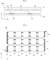
- FIG. 1 is a schematic sectional view of a solar cell module (hereinafter referred to as a "module") according to one embodiment.
- a module 200 shown in FIG. 1 includes a solar cell string in which plurality of solar cells (hereinafter referred to as "cells”) 102, 103 and 104 are electrically connected through wiring members 83 and 84.
- a light-receiving-surface protection member 91 is disposed on the light-receiving side (the upper side in FIG. 1 ) of the solar cell string, and a back-surface protection member 92 is disposed on the back side (the lower side in FIG. 1 ) of the solar cell string.
- the solar cell string is encapsulated by filling the space between the protection members 91 and 92 with an encapsulant 95.
- a back contact solar cell As the cell, a back contact solar cell (back contact cell) is used.
- the back contact cell has a p-type semiconductor layer and an n-type semiconductor layer on the back side of a semiconductor substrate of crystalline silicon or the like, and a metal electrode is disposed on each of the p-type semiconductor layer and the n-type semiconductor layer.
- the metal electrode can be formed by a known method such as printing or plating. For example, an Ag electrode formed by screen printing of an Ag paste, a copper-plated electrode formed by electroplating, or the like is preferred.
- the back contact cell does not have a metal electrode on the light-receiving surface of the semiconductor substrate, and photocarriers (holes and electrons) generated in the semiconductor substrate are collected by the metal electrode disposed on the back side of the semiconductor substrate. Since the back contact cell does not have a metal electrode on the light-receiving surface, the entire surface of the cell is uniformly colored black when the cell is viewed from the light-receiving side, so that an excellent visuality is exhibited.
- Solar cells generally has, though not limited to, a rectangular shape in plan view.
- the term "rectangular shape” includes a square shape and an oblong shape. The "rectangular shape” is not required to be a perfectly square shape or oblong shape, and for example, the semiconductor substrate may have a semi-square shape (a rectangular shape having rounded corners, or a shape having a notched portion).
- the light-receiving surface of the cell preferably has a recessed and projected structure for improving conversion efficiency by increasing the amount of light captured in the semiconductor substrate.
- the shape of the projection is preferably a quadrangular pyramidal shape.
- the quadrangular pyramid-shaped projections are formed by, for example, subjecting a surface of the single-crystalline silicon substrate to anisotropic etching treatment.
- the height of the projection on the light-receiving surface of the cell is, for example, about 0.5 to 10 ⁇ m, preferably about 1 to 5 ⁇ m.
- the back surface of the cell may also have a recessed and projected structure.
- FIG. 2 is plan view of a back surface of a solar cell grid in which a plurality of back contact cells are arranged in a grid shape.
- solar cell strings 100, 110, and 120 in which a plurality of cells are connected along a first direction (x direction) are arranged side by side along a second direction (y direction) orthogonal to the first direction.
- the solar cell string 100 includes a plurality of cells 101 to 105 arranged in a first direction. Electrodes disposed on the back side of cells are electrically connected through wiring members 82 to 85 to form a solar cell string. A plurality of cells is connected in series by connecting the p-side electrode of one of two adjacent cells to the n-side electrode of the other cell through the wiring member. The cells can also be connected in parallel by connecting n-side electrodes or p-side electrodes of adjacent cells.
- the wiring member 81 arranged at one end portion in the first direction includes a lead wire 81a which can be connected to an external circuit.
- the wiring member 86 arranged at the other end portion in the first direction is connected to the solar cell string 110 adjacent in the second direction.
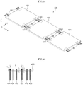
- FIG. 3 is a schematic perspective view of the solar cell string 100.
- adjacent cells are connected by two wiring members.
- the number of wiring members arranged between adjacent cells is appropriately set according to the shape of the electrode pattern of the cell or the like.
- a portion 831, 841 of a wiring member 83, 84 positioned in a gap between adjacent solar cells is exposed to the light-receiving side, and thus is visible from the outside.
- a wiring member which is black on at least the light-receiving side is used, metal reflection of the wiring member is reduced, and the visual impression between the exposed portion of the wiring member and the cell is unified, so that the visuality of the solar cell module is improved.
- the wiring member has a first principal surface, a second principal surface and lateral surfaces.
- the wiring member is a braided wire having a flat-shaped cross-section and composed of a plurality of metal element wires, and has an electroconductive black layer disposed on the entire first principal surface.
- the wiring member is arranged in such a manner that the first principal surface is on the light-receiving side, and the first principal surface of the wiring member is connected to the back electrode of the cell.
- the width of the wiring member is, for example, about 1 mm to 5 mm, and the thickness of the wiring member is, for example, about 50 ⁇ m to 500 ⁇ m.
- the diameter of the metal element wire forming the braided wire is, for example, about 10 to 200 ⁇ m.
- the number of metal element wires forming the braided wire is about 10 to 500.
- the back surfaces of adjacent cells are connected to each other by a wiring member, and therefore shadowing loss does not cause a problem even when the wiring member has a large width (area).
- the contact area between the cell and the wiring member can be increased to reduce contact resistance.
- bonding reliability between the cell and the wiring member is improved, leading to improvement of the durability of the solar cell module.
- a connection failure such as peeling of the wiring member easily occurs due to a difference in linear expansion coefficient between the wiring member and the cell which is caused by a temperature change.
- a braided wire composed of a plurality of element wires is flexible and stretchable, so that stress caused by a difference in linear expansion due to a temperature change can be absorbed and scattered by the wiring member. Thus, even when the contact area between the cell and the wiring member is increased, high bonding reliability can be maintained.
- the braided wire having a flat-shaped cross-section may be formed by knitting a plurality of metal element wires in such a manner as to form a flat shape, or a braided wire obtained by knitting a plurality of element wires into a cylindrical shape may be made to have a flat-shaped cross-section by rolling processing.
- Examples of the method for knitting metal element wires include plain knitting, single braiding, double braiding, triple braiding, Denbigh knitting, cord knitting, atlas knitting, chain knitting, crochet knitting, fourth-carrier braiding, six-carrier braiding, eight-carrier braiding, wickerwork, triaxial weaving, three-thread braiding, right knotting, left knotting, warp knotting, weft knotting, oblique knitting, rubber knitting, moss knitting, stockinette knitting and garter knitting.
- the metal material forming the metal element wire is not particularly limited as long as it is electroconductive.
- the material of the wiring member has a low resistivity for reducing an electrical loss caused by resistance of the wiring member.
- copper or a copper alloy containing copper as a main component is preferable because the material is inexpensive.
- the wiring member has an electroconductive black layer at least on the entire first principal surface.
- the first principal surface is provided with the electroconductive black layer, light reflection at portions 831 and 841 positioned in gaps between cells and exposed to the light-receiving surface is reduced.
- the colors of the exposed portion of the wiring member and the cell are unified.
- the visible light reflectance of the first principal surface of the wiring member is preferably as small as the reflectance of the light-receiving surface of the cell, and is preferably 10% or less.
- the black layer described in this specification a desired visible light reflectance can be attained.
- the black layer is composed of an electroconductive material containing a metal, it is difficult to completely eliminate surface reflection.
- the surface of the braided wire composed of a plurality of metal element wires has irregularities caused by the shape of the metal element wires (generally a circular cross section), light is irregularly reflected at the surface of the wiring member.
- light reflected at the surface of the wiring member is visible as hazy scattered light to the viewer on the light-receiving side, and reflected light with metallic luster is hardly visible. Therefore, even when light reflection at the wiring member cannot be completely inhibited, deterioration of the visuality, which is caused by reflected light from the wiring member hardly occurs.
- reflected light at the light-receiving surface of the cell is closely similar in visual impression to reflected light at the first principal surface of the wiring member including a braided wire, and therefore reflected light from the wiring member is inconspicuous, so that the visuality of the module is improved.
- the electroconductive black layer is formed on the first principal surface in not only the exposed portions 831 and 841 between adjacent cells but also the connection portion to the cell. Since the black layer for anti-reflection has electroconductivity, contact resistance between the electrode of the cell and the wiring member is small, so that the power generation loss in the module can be reduced. Since the electroconductive black layer is formed on the entire first principal surface of the wiring member, precise alignment is not required at the time of connecting the cell to the wiring member. Thus, the productivity and the yield of the solar cell module can be improved.
- the electroconductive black layer may be formed on the lateral surface and the second principal surface of the wiring member as in the case of the first principal surface. In a portion which is not exposed to the surface of the wiring member, there may be a non-blackening-treated region where the electroconductive black layer is not provided.
- a braided wire having an electroconductive black layer can be obtained by, for example, applying electroconductive-blackening-treatment to a braided wire obtained by knitting metal element wires.
- a braided wire may be obtained by knitting metal element wires subjected to electroconductive-blackening-treatment.
- a dry process such as a sputtering method, a CVD method or a vacuum vapor deposition method; or a wet process such as application of a metal paste material or electroplating or electroless plating (autocatalysis plating or displacement plating) is applicable.
- Examples of the material of the electroconductive black layer formed on the surface of the wiring member include alloys of copper and nickel, chromium, zinc, palladium or the like, metallic palladium or palladium alloys, metal oxides, and metals in which a black material such as carbon nanotubes or carbon is dispersed.
- a metal layer containing palladium is formed as the electroconductive black layer because it is excellent in electroconductivity and excellent in adhesion to a metal material such as copper, and has high wettability to solder.
- the method for forming a metal layer containing palladium on a wiring member (or on a metal element wires constituting the wiring member) is preferably electroless plating.
- an electroless plating solution for example, an aqueous solution containing a palladium salt, a halide ion, and a nitrogen-containing compound is used.
- the electroless plating solution is preferably an acidic aqueous solution having a pH of about 0 to 5.
- the palladium salt examples include palladium chloride, palladium sulfate, palladium oxide, palladium iodide, palladium bromide, palladium nitrate, palladium acetate, tetraamine palladium chloride, dinitrodiamine palladium and dichlorodiethylenediamine palladium.
- concentration of palladium in the electroless plating solution is preferably about 0.001 to 5 g/L.
- halide ion examples include a chloride ion, a bromide ion and an iodide ion, with a chloride ion being preferable.
- halide ion source for adding a halide ion in the electroless plating solution include halogenated hydroacids such as hydrochloric acid, hydrobromic acid and hydroiodic acid; alkali metal salts such as sodium chloride and potassium bromide; alkaline earth metal salts such as magnesium chloride and calcium iodide; and ammonium chloride and ammonium bromide.
- concentration of halide ions in the electroless plating solution is preferably about 1 to 300 g/L.
- the nitrogen-containing compound is preferably a polyamine such as an alkylene diamine, polyalkylene polyamine, polyamide polyamine or a crosslinked product of polyamide polyamine.
- the content of the nitrogen-containing compound in the electroless plating solution is preferably about 0.01 to 200 g/L.
- An electroconductive black layer (electroless palladium plated layer) containing palladium is formed by bringing the electroless plating solution into contact with an object for blackening-treatment (wiring member or metal element wire).
- an object for blackening-treatment may be immersed in the electroless plating solution to bring the electroless plating solution into contact with the object for blackening-treatment.
- the electroless plating solution may be sprayed to the surface of the object for blackening-treatment.
- a wiring member is obtained in which an electroconductive black layer is formed on the entire first principal surface, lateral surfaces and second principal surface, i.e . the entire exposed portion to the surfaces of metal element wires.
- the electroconductive black layer is also formed on the portion which is not exposed to the surface of the wiring member of the metal element wire.
- the portion which is not exposed to the braided wire surface of metal element wires is a non-blackening-treated region on which no electroconductive black layer is formed.
- a black layer is formed on a region visible from outside the wiring member (first principal surfaces of exposed portions 831 and 841). Therefore, the portion which is not exposed to the surface of the wiring member of the metal element wires may be either a blackening-treated region or a non-blackening-treated region.
- the treatment temperature in electroless plating is, for example, preferably about 10 to 60°C, more preferably about 20 to 50°C.
- the treatment time is, for example, preferably about 10 seconds to 10 minutes.
- electroconductive-blackening-treatment Before electroconductive-blackening-treatment is performed by electroless plating, degreasing treatment, acid treatment or the like may be performed for the purpose of removing contaminants on the surface and oxide films on the surface of an object for plating treatment as necessary.
- the plated material after electroless plating may be rinsed with water and dried.
- a back contact cell and wiring member including a braided wire subjected to blackening-treatment are prepared, and adjacent cells are connected to each other through the wiring member to prepare a solar cell string.
- a back electrode of the cell is connected to a first principal surface of the wiring member with an electroconductive connection material such as an electroconductive film or an electroconductive paste interposed therebetween.
- solder When solder is used as an electroconductive connection material, solder may be welded onto the first principal surface of the wiring member or the electrode of the cell in advance. When solder is welded onto the first principal surface of the wiring member in advance, metallic luster of the solder is visible from the light-receiving surface of the module, leading to deterioration of the visuality if the solder is deposited on exposed portions 831 and 841 between adjacent cells.
- solder When solder is welded onto the first principal surface of the wiring member in advance, it is necessary that a region of solder welded onto the wiring member be adjusted so as to prevent protrusion of solder to a visible region, and the wiring member and the cell be precisely aligned during solder connection.
- a method in which solder is disposed on the electrode of the cell, and the wiring member is connected onto the solder does not require precise alignment for preventing protrusion of solder to a portion in which the wiring member is exposed between cells.
- welded solder, a solder paste, or the like is disposed on the electrode of the cell, and the electrode is connected to the wiring member.
- a solder connection pad When the cell is connected to the wiring member with solder, a solder connection pad may be disposed in a portion of the peripheral edge in the cell surface where finger electrodes are gathered.
- a wiring member including a braided wire of a plurality of metal element wires molten solder is easily retained in a space between metal element wires due to a capillary phenomenon.
- spreading of solder is suppressed, so that protrusion of solder to the exposed portion of the wiring member between cells hardly occurs. Since solder hardly spreads, the area of the solder connection pad may be reduced.
- a wiring member which is used for a general module and composed of a plate-shaped metal member is rigid, so that it may be difficult to align the wiring member and the solder connection pad when the area of the solder connection pad is reduced.
- a braided wire composed of a plurality of element wires is flexible and stretchable, so that even when positional deviation occurs between adjacent cells, by bending the wiring member, alignment of the wiring member on the solder connection pad can be carried out.
- the wiring member including a braided wire is flexible and stretchable, and therefore can be adapted to alignment in a string connection direction (x direction).
- the wiring member including a braided wire can be bent in cell thickness direction (z direction), so that stress in the thickness direction can be scattered, and even when the cell is warped, defects such as breakage at the time of handling a string after connection of a plurality of cells can be suppressed.
- the solar cell string with a plurality of cells connected by the wiring member is sandwiched between a light-receiving-surface protection member 91 and a back-surface protection member 92 with an encapsulant 95 interposed between each of the protection members and the solar cell string, thereby forming the solar cell module.
- a laminate in which the light-receiving-side encapsulant, the solar cell string, the back-side encapsulant and the back-surface protection member are mounted in this order on the light-receiving-surface protection member is heated at predetermined conditions to cure the encapsulant.
- a plurality of solar cell strings may be connected to form a solar cell grid as shown in FIG. 2 .
- a transparent resin such as a polyethylene-based resin composition mainly composed of an olefin-based elastomer, polypropylene, an ethylene/ ⁇ -olefin copolymer, an ethylene/vinyl acetate copolymer (EVA), an ethylene/vinyl acetate/triallyl isocyanurate (EVAT), polyvinyl butyrate (PVB), silicon, urethane, acrylic or epoxy is used as the encapsulant 95.
- EVA ethylene/vinyl acetate copolymer
- EVAT ethylene/vinyl acetate/triallyl isocyanurate
- PVB polyvinyl butyrate
- silicon urethane
- acrylic or epoxy is used as the encapsulant 95.
- Materials of the encapsulants on the light-receiving side and the back side may be the same or different.
- the light-receiving-surface protection member 91 which is light-transmissive, glass, transparent plastic or the like is used.
- the back-surface protection member 92 a black sheet having a black-color principal surface on the light-receiving side is used.
- a black sheet By using a black sheet as the back-surface protection member, not only cells but also both the wiring member and the back-surface protection member exposed between adjacent cells are uniformly colored black. Therefore, a module which is entirely uniformly colored black, and has an excellent visuality can be obtained.
- the black sheet for example, a sheet including a black resin layer is used.
- the black resin layer has visible light-absorbency, and mainly absorbs visible light having a wavelength of 800 nm or less.
- the visible light transmittance of the black resin layer is preferably 10% or less.
- a resin composition containing a thermoplastic resin such as a polyolefin-based resin, a polyester-based resin, an acryl-based resin, a fluororesin or an ethylene-vinyl acetate resin and a colorant such as a pigment or a dye is preferably used.
- the black sheet to be used as the back-surface protection member 92 may have infrared ray reflectivity while absorbing visible light.
- infrared rays contained in light passing through gaps between adjacent cells and light transmitted through the cells can be reflected to the light-receiving side, and used for power generation.
- the black sheet having infrared ray reflectivity include those obtained by stacking a black resin layer and infrared ray reflecting layer, and those containing a pigment having infrared ray reflectivity in a black resin layer.
- a resin layer composed of a resin composition containing a white pigment having infrared ray reflectivity, such as titanium oxide, a metal foil having infrared ray reflectivity (e.g., aluminum or silver), or the like is used.
- a white pigment having infrared ray reflectivity such as titanium oxide
- a metal foil having infrared ray reflectivity e.g., aluminum or silver
- the allowable tolerance of the patterning accuracy and alignment accuracy of electrodes of the cell can be increased, and breakage during handling can be suppressed, so that the module production efficiency and yield can be improved.
- stress caused by a difference in linear expansion coefficient due to a temperature change can be absorbed and scattered by the wiring member including a braided wire.
- a module is obtained which hardly suffers from a connection failure of a wiring member due to a dimension change, etc. even when subjected to a temperature cycle test, and is excellent in durability.
- a braided wire (width: about 2 mm, thickness: about 200 ⁇ m) having a flat-shaped cross-section and obtained by knitting total 64 copper wires, where four element wires each having a diameter of about 60 ⁇ m and composed of copper were used as a unit, was subjected to blackening-treatment, and evaluated.
- Example 1 the above-described braided wire was immersed in an electroless palladium plating solution containing 0.5 g/L of palladium ("OPC Black Copper” manufactured by Okuno Chemical Industries Co., Ltd.), so that electroless plating was performed at room temperature to obtain a braided wire having an electroconductive black layer on the entire surface. On element wires inside the braided wire, an electroconductive black layer was not formed, and copper was exposed. In the obtained braided wire, the entire surface was black, and favorable solder wettability similar to that of the braided wire before blackening-treatment was exhibited.
- OPC Black Copper manufactured by Okuno Chemical Industries Co., Ltd.
- Example 2 with the braided wire subjected to black chromium treatment, Example 3 with the braided wire subjected to black nickel treatment and Example 4 with the braided wire subjected to black oxide treatment by strong alkali boiling (formation of fine irregular films of copper oxide), evaluation was performed in the same manner as in Example 1.
- Example 2 with the braided wire subjected to black chromium treatment
- Example 3 with the braided wire subjected to black nickel treatment
- Example 4 with the braided wire subjected to black oxide treatment by strong alkali boiling (formation of fine irregular films of copper oxide) evaluation was performed in the same manner as in Example 1.
- the entire surface of the wiring member was black, but solder wetting did not occur.
- FIG. 4 As schematically shown in FIG. 4 , twenty wiring members 401 to 420 were solder-connected at equal intervals in a length direction of a 3 mm-wide belt-shaped copper-plated film 450 to prepare a sample for evaluation of contact resistance.
- One terminal of a two-terminal resistance meter was brought into contact with a contact point 1 between the wiring member 401 and the copper-plated film 450, and the other terminal was brought into contact with a contact point x between another wiring member and the copper-plated film to measure the resistance between the two points.
- the resistance was measured while the position at which the other terminal was brought into contact with the wiring member was sequentially changed to positions on the wiring members 402 to 420, the distance d between the terminals and the resistance were plotted, and linear approximation was performed by the least squares method.
- the contact resistance when a 1.5 mm-wide plate-shaped copper foil was used as a wiring member was 2.3 times the contact resistance when a braided wire which was not subjected to blackening-treatment was used as a wiring member.
- the contact resistance was 1.1 times that of a braided wire which was not subjected to blackening-treatment. There was no significant change in contact resistance before and after the blackening-treatment.
- a wiring member composed of a braided wire has lower contact resistance with an electrode material in solder connection as compared to a plate-shaped wiring member, and even in the case of a braided wire subjected to blackening-treatment with palladium, the property is maintained.
Landscapes
- Photovoltaic Devices (AREA)
Applications Claiming Priority (2)
| Application Number | Priority Date | Filing Date | Title |
|---|---|---|---|
| JP2016238368 | 2016-12-08 | ||
| PCT/JP2017/034557 WO2018105202A1 (fr) | 2016-12-08 | 2017-09-25 | Module de cellules solaires |
Publications (3)
| Publication Number | Publication Date |
|---|---|
| EP3553832A1 true EP3553832A1 (fr) | 2019-10-16 |
| EP3553832A4 EP3553832A4 (fr) | 2020-06-03 |
| EP3553832B1 EP3553832B1 (fr) | 2022-05-18 |
Family
ID=62492185
Family Applications (1)
| Application Number | Title | Priority Date | Filing Date |
|---|---|---|---|
| EP17879377.4A Active EP3553832B1 (fr) | 2016-12-08 | 2017-09-25 | Module de cellules solaires |
Country Status (5)
| Country | Link |
|---|---|
| US (1) | US20190341515A1 (fr) |
| EP (1) | EP3553832B1 (fr) |
| JP (1) | JP7076376B2 (fr) |
| CN (1) | CN110024138B (fr) |
| WO (1) | WO2018105202A1 (fr) |
Cited By (1)
| Publication number | Priority date | Publication date | Assignee | Title |
|---|---|---|---|---|
| CN114649443A (zh) * | 2022-03-03 | 2022-06-21 | 浙江爱旭太阳能科技有限公司 | 背接触太阳能电池串及其制备方法、电池组件及光伏系统 |
Families Citing this family (6)
| Publication number | Priority date | Publication date | Assignee | Title |
|---|---|---|---|---|
| NL2021711B1 (en) * | 2018-09-26 | 2020-05-07 | Atlas Technologies Holding Bv | A method of producing a solar panel curved in two directions. |
| JP2021059697A (ja) * | 2019-10-09 | 2021-04-15 | 日東電工株式会社 | フッ素樹脂シート及び粘着テープ |
| US20240194820A1 (en) * | 2020-12-30 | 2024-06-13 | Risen Energy Co. Ltd | Packaging method for solar cell module, connection method for solar cell string, solar cell module, and preparation method therefor |
| JPWO2023054229A1 (fr) * | 2021-09-28 | 2023-04-06 | ||
| CN222706430U (zh) * | 2024-02-07 | 2025-04-01 | 隆基绿能科技股份有限公司 | 一种光伏组件和光伏系统 |
| JP2026046383A (ja) * | 2024-09-02 | 2026-03-13 | シャープエネルギーソリューション株式会社 | 太陽電池モジュール |
Family Cites Families (25)
| Publication number | Priority date | Publication date | Assignee | Title |
|---|---|---|---|---|
| JPH08330615A (ja) * | 1995-05-30 | 1996-12-13 | Canon Inc | 直列型太陽電池およびその製造方法 |
| JP4526223B2 (ja) * | 2001-06-29 | 2010-08-18 | シャープ株式会社 | 配線部材ならびに太陽電池モジュールおよびその製造方法 |
| JP2005191479A (ja) | 2003-12-26 | 2005-07-14 | Sekisui Jushi Co Ltd | 太陽電池モジュール |
| US7390961B2 (en) | 2004-06-04 | 2008-06-24 | Sunpower Corporation | Interconnection of solar cells in a solar cell module |
| JP2006165148A (ja) * | 2004-12-06 | 2006-06-22 | Canon Inc | 光起電力素子、光起電力素子集合体、光起電力素子モジュール、及び、それらの製造方法 |
| JP2009176782A (ja) | 2008-01-21 | 2009-08-06 | Sanyo Electric Co Ltd | 太陽電池モジュール |
| GB2458961A (en) * | 2008-04-04 | 2009-10-07 | Rec Solar As | Flexible interconnectors comprising conductive fabric between solar cells |
| JP2010087011A (ja) | 2008-09-29 | 2010-04-15 | Kyocera Corp | 太陽電池モジュールおよびその製造方法 |
| JP2010093040A (ja) * | 2008-10-08 | 2010-04-22 | Bridgestone Corp | 光透過性電磁波シールド材及びその製造方法 |
| GB2467361A (en) * | 2009-01-30 | 2010-08-04 | Renewable Energy Corp Asa | Contact and interconnect for a solar cell |
| JP5449849B2 (ja) * | 2009-04-30 | 2014-03-19 | シャープ株式会社 | 太陽電池およびその製造方法 |
| KR101130197B1 (ko) * | 2009-09-28 | 2012-03-30 | 엘지전자 주식회사 | 태양전지 모듈 및 그 제조 방법 |
| KR101145927B1 (ko) * | 2009-09-28 | 2012-05-15 | 엘지전자 주식회사 | 태양전지 모듈 및 그 제조 방법 |
| WO2011148931A1 (fr) * | 2010-05-28 | 2011-12-01 | コニカミノルタホールディングス株式会社 | Électrode pour dispositif électronique organique |
| US8802479B2 (en) * | 2010-06-03 | 2014-08-12 | NuvoSun, Inc. | Solar cell interconnection method using a flat metallic mesh |
| WO2012135052A1 (fr) * | 2011-03-25 | 2012-10-04 | Kevin Michael Coakley | Interconnexion à feuilles pour cellules solaires à contact arrière |
| US9490376B2 (en) | 2011-09-29 | 2016-11-08 | Lg Electronics Inc. | Solar cell module |
| JP2013161855A (ja) | 2012-02-02 | 2013-08-19 | Sharp Corp | 太陽電池用インターコネクタおよびインターコネクタ付き太陽電池セル |
| EP2660878B1 (fr) * | 2012-05-04 | 2014-12-31 | Sol Invictus Energy | Matières tissées hybrides utiles dans la production de cellules solaires à contact arrière |
| CN103972317A (zh) * | 2013-01-31 | 2014-08-06 | 无锡尚德太阳能电力有限公司 | 一种太阳电池用互连条及其制造方法及太阳电池组件 |
| JP5829746B1 (ja) * | 2014-04-04 | 2015-12-09 | キヤノン・コンポーネンツ株式会社 | 導電膜及びその製造方法並びにめっき皮膜付樹脂製品及びその製造方法 |
| WO2016035897A1 (fr) * | 2014-09-05 | 2016-03-10 | 日産化学工業株式会社 | Agent de sous-couche de placage autocatalytique photosensible |
| US10636924B2 (en) * | 2014-11-26 | 2020-04-28 | Sunpower Corporation | Solar module interconnect |
| CN104716208A (zh) | 2014-12-16 | 2015-06-17 | 浙江宝利特新能源股份有限公司 | 一种光伏组件生产制造工艺 |
| WO2016103507A1 (fr) * | 2014-12-26 | 2016-06-30 | 日本テクノリード株式会社 | Substrat maillé métallique, et procédé de fabrication associé |
-
2017
- 2017-09-25 JP JP2018554834A patent/JP7076376B2/ja active Active
- 2017-09-25 US US16/466,739 patent/US20190341515A1/en not_active Abandoned
- 2017-09-25 WO PCT/JP2017/034557 patent/WO2018105202A1/fr not_active Ceased
- 2017-09-25 CN CN201780068451.0A patent/CN110024138B/zh active Active
- 2017-09-25 EP EP17879377.4A patent/EP3553832B1/fr active Active
Cited By (2)
| Publication number | Priority date | Publication date | Assignee | Title |
|---|---|---|---|---|
| CN114649443A (zh) * | 2022-03-03 | 2022-06-21 | 浙江爱旭太阳能科技有限公司 | 背接触太阳能电池串及其制备方法、电池组件及光伏系统 |
| CN114649443B (zh) * | 2022-03-03 | 2024-04-16 | 浙江爱旭太阳能科技有限公司 | 背接触太阳能电池串及其制备方法、电池组件及光伏系统 |
Also Published As
| Publication number | Publication date |
|---|---|
| EP3553832B1 (fr) | 2022-05-18 |
| JP7076376B2 (ja) | 2022-05-27 |
| JPWO2018105202A1 (ja) | 2019-10-24 |
| US20190341515A1 (en) | 2019-11-07 |
| WO2018105202A1 (fr) | 2018-06-14 |
| EP3553832A4 (fr) | 2020-06-03 |
| CN110024138A (zh) | 2019-07-16 |
| CN110024138B (zh) | 2022-12-20 |
Similar Documents
| Publication | Publication Date | Title |
|---|---|---|
| EP3553832B1 (fr) | Module de cellules solaires | |
| JP6697456B2 (ja) | 結晶シリコン太陽電池モジュールおよびその製造方法 | |
| US9728658B2 (en) | Solar cell module | |
| US9691925B2 (en) | Light receiving element module and manufacturing method therefor | |
| CN109819681B (zh) | 太阳能电池模块 | |
| US20200091362A1 (en) | Solar cell module and method for producing same | |
| US20130112234A1 (en) | Solar cell module | |
| US20200098943A1 (en) | Solar cell module and manufacturing method thereof | |
| WO2014002249A1 (fr) | Cellule solaire, module de cellules solaires et procédé de production de cellule solaire | |
| WO2014192272A1 (fr) | Module de cellules solaires | |
| JP6677801B2 (ja) | 結晶シリコン系太陽電池およびその製造方法、ならびに太陽電池モジュール | |
| WO2015166780A1 (fr) | Cellule solaire en silicium cristallin, module de cellule solaire en silicium cristallin, et procédés de fabrication correspondants | |
| JP6745089B2 (ja) | 太陽電池モジュール | |
| CN110943140A (zh) | 一种光伏元件间的连接器、光伏元件组及光伏系统 | |
| JP6937762B2 (ja) | 太陽電池用配線材および太陽電池モジュール | |
| KR20130011328A (ko) | 리본 및 이를 구비한 태양전지 모듈 | |
| JP2016086154A (ja) | 太陽電池モジュール | |
| JP2015185695A (ja) | 太陽電池モジュール及びその製造方法 | |
| US20170092797A1 (en) | Solar cell module | |
| WO2020031574A1 (fr) | Module de cellules solaires | |
| KR20110049669A (ko) | 태양 전지 모듈 | |
| KR20190014880A (ko) | 태양 전지 패널 | |
| KR20140040347A (ko) | 태양 전지 및 이의 제조 방법 |
Legal Events
| Date | Code | Title | Description |
|---|---|---|---|
| STAA | Information on the status of an ep patent application or granted ep patent |
Free format text: STATUS: THE INTERNATIONAL PUBLICATION HAS BEEN MADE |
|
| PUAI | Public reference made under article 153(3) epc to a published international application that has entered the european phase |
Free format text: ORIGINAL CODE: 0009012 |
|
| STAA | Information on the status of an ep patent application or granted ep patent |
Free format text: STATUS: REQUEST FOR EXAMINATION WAS MADE |
|
| 17P | Request for examination filed |
Effective date: 20190627 |
|
| AK | Designated contracting states |
Kind code of ref document: A1 Designated state(s): AL AT BE BG CH CY CZ DE DK EE ES FI FR GB GR HR HU IE IS IT LI LT LU LV MC MK MT NL NO PL PT RO RS SE SI SK SM TR |
|
| AX | Request for extension of the european patent |
Extension state: BA ME |
|
| DAV | Request for validation of the european patent (deleted) | ||
| DAX | Request for extension of the european patent (deleted) | ||
| A4 | Supplementary search report drawn up and despatched |
Effective date: 20200508 |
|
| RIC1 | Information provided on ipc code assigned before grant |
Ipc: H01L 31/05 20140101AFI20200501BHEP |
|
| GRAP | Despatch of communication of intention to grant a patent |
Free format text: ORIGINAL CODE: EPIDOSNIGR1 |
|
| STAA | Information on the status of an ep patent application or granted ep patent |
Free format text: STATUS: GRANT OF PATENT IS INTENDED |
|
| INTG | Intention to grant announced |
Effective date: 20211130 |
|
| GRAS | Grant fee paid |
Free format text: ORIGINAL CODE: EPIDOSNIGR3 |
|
| GRAA | (expected) grant |
Free format text: ORIGINAL CODE: 0009210 |
|
| STAA | Information on the status of an ep patent application or granted ep patent |
Free format text: STATUS: THE PATENT HAS BEEN GRANTED |
|
| AK | Designated contracting states |
Kind code of ref document: B1 Designated state(s): AL AT BE BG CH CY CZ DE DK EE ES FI FR GB GR HR HU IE IS IT LI LT LU LV MC MK MT NL NO PL PT RO RS SE SI SK SM TR |
|
| REG | Reference to a national code |
Ref country code: GB Ref legal event code: FG4D |
|
| REG | Reference to a national code |
Ref country code: CH Ref legal event code: EP |
|
| REG | Reference to a national code |
Ref country code: IE Ref legal event code: FG4D |
|
| REG | Reference to a national code |
Ref country code: DE Ref legal event code: R096 Ref document number: 602017057736 Country of ref document: DE |
|
| REG | Reference to a national code |
Ref country code: AT Ref legal event code: REF Ref document number: 1493641 Country of ref document: AT Kind code of ref document: T Effective date: 20220615 |
|
| REG | Reference to a national code |
Ref country code: LT Ref legal event code: MG9D |
|
| REG | Reference to a national code |
Ref country code: NL Ref legal event code: MP Effective date: 20220518 |
|
| REG | Reference to a national code |
Ref country code: AT Ref legal event code: MK05 Ref document number: 1493641 Country of ref document: AT Kind code of ref document: T Effective date: 20220518 |
|
| PG25 | Lapsed in a contracting state [announced via postgrant information from national office to epo] |
Ref country code: SE Free format text: LAPSE BECAUSE OF FAILURE TO SUBMIT A TRANSLATION OF THE DESCRIPTION OR TO PAY THE FEE WITHIN THE PRESCRIBED TIME-LIMIT Effective date: 20220518 Ref country code: PT Free format text: LAPSE BECAUSE OF FAILURE TO SUBMIT A TRANSLATION OF THE DESCRIPTION OR TO PAY THE FEE WITHIN THE PRESCRIBED TIME-LIMIT Effective date: 20220919 Ref country code: NO Free format text: LAPSE BECAUSE OF FAILURE TO SUBMIT A TRANSLATION OF THE DESCRIPTION OR TO PAY THE FEE WITHIN THE PRESCRIBED TIME-LIMIT Effective date: 20220818 Ref country code: NL Free format text: LAPSE BECAUSE OF FAILURE TO SUBMIT A TRANSLATION OF THE DESCRIPTION OR TO PAY THE FEE WITHIN THE PRESCRIBED TIME-LIMIT Effective date: 20220518 Ref country code: LT Free format text: LAPSE BECAUSE OF FAILURE TO SUBMIT A TRANSLATION OF THE DESCRIPTION OR TO PAY THE FEE WITHIN THE PRESCRIBED TIME-LIMIT Effective date: 20220518 Ref country code: HR Free format text: LAPSE BECAUSE OF FAILURE TO SUBMIT A TRANSLATION OF THE DESCRIPTION OR TO PAY THE FEE WITHIN THE PRESCRIBED TIME-LIMIT Effective date: 20220518 Ref country code: GR Free format text: LAPSE BECAUSE OF FAILURE TO SUBMIT A TRANSLATION OF THE DESCRIPTION OR TO PAY THE FEE WITHIN THE PRESCRIBED TIME-LIMIT Effective date: 20220819 Ref country code: FI Free format text: LAPSE BECAUSE OF FAILURE TO SUBMIT A TRANSLATION OF THE DESCRIPTION OR TO PAY THE FEE WITHIN THE PRESCRIBED TIME-LIMIT Effective date: 20220518 Ref country code: ES Free format text: LAPSE BECAUSE OF FAILURE TO SUBMIT A TRANSLATION OF THE DESCRIPTION OR TO PAY THE FEE WITHIN THE PRESCRIBED TIME-LIMIT Effective date: 20220518 Ref country code: BG Free format text: LAPSE BECAUSE OF FAILURE TO SUBMIT A TRANSLATION OF THE DESCRIPTION OR TO PAY THE FEE WITHIN THE PRESCRIBED TIME-LIMIT Effective date: 20220818 Ref country code: AT Free format text: LAPSE BECAUSE OF FAILURE TO SUBMIT A TRANSLATION OF THE DESCRIPTION OR TO PAY THE FEE WITHIN THE PRESCRIBED TIME-LIMIT Effective date: 20220518 |
|
| PG25 | Lapsed in a contracting state [announced via postgrant information from national office to epo] |
Ref country code: RS Free format text: LAPSE BECAUSE OF FAILURE TO SUBMIT A TRANSLATION OF THE DESCRIPTION OR TO PAY THE FEE WITHIN THE PRESCRIBED TIME-LIMIT Effective date: 20220518 Ref country code: PL Free format text: LAPSE BECAUSE OF FAILURE TO SUBMIT A TRANSLATION OF THE DESCRIPTION OR TO PAY THE FEE WITHIN THE PRESCRIBED TIME-LIMIT Effective date: 20220518 Ref country code: LV Free format text: LAPSE BECAUSE OF FAILURE TO SUBMIT A TRANSLATION OF THE DESCRIPTION OR TO PAY THE FEE WITHIN THE PRESCRIBED TIME-LIMIT Effective date: 20220518 Ref country code: IS Free format text: LAPSE BECAUSE OF FAILURE TO SUBMIT A TRANSLATION OF THE DESCRIPTION OR TO PAY THE FEE WITHIN THE PRESCRIBED TIME-LIMIT Effective date: 20220918 |
|
| PG25 | Lapsed in a contracting state [announced via postgrant information from national office to epo] |
Ref country code: SM Free format text: LAPSE BECAUSE OF FAILURE TO SUBMIT A TRANSLATION OF THE DESCRIPTION OR TO PAY THE FEE WITHIN THE PRESCRIBED TIME-LIMIT Effective date: 20220518 Ref country code: SK Free format text: LAPSE BECAUSE OF FAILURE TO SUBMIT A TRANSLATION OF THE DESCRIPTION OR TO PAY THE FEE WITHIN THE PRESCRIBED TIME-LIMIT Effective date: 20220518 Ref country code: RO Free format text: LAPSE BECAUSE OF FAILURE TO SUBMIT A TRANSLATION OF THE DESCRIPTION OR TO PAY THE FEE WITHIN THE PRESCRIBED TIME-LIMIT Effective date: 20220518 Ref country code: EE Free format text: LAPSE BECAUSE OF FAILURE TO SUBMIT A TRANSLATION OF THE DESCRIPTION OR TO PAY THE FEE WITHIN THE PRESCRIBED TIME-LIMIT Effective date: 20220518 Ref country code: DK Free format text: LAPSE BECAUSE OF FAILURE TO SUBMIT A TRANSLATION OF THE DESCRIPTION OR TO PAY THE FEE WITHIN THE PRESCRIBED TIME-LIMIT Effective date: 20220518 Ref country code: CZ Free format text: LAPSE BECAUSE OF FAILURE TO SUBMIT A TRANSLATION OF THE DESCRIPTION OR TO PAY THE FEE WITHIN THE PRESCRIBED TIME-LIMIT Effective date: 20220518 |
|
| REG | Reference to a national code |
Ref country code: DE Ref legal event code: R097 Ref document number: 602017057736 Country of ref document: DE |
|
| PLBE | No opposition filed within time limit |
Free format text: ORIGINAL CODE: 0009261 |
|
| STAA | Information on the status of an ep patent application or granted ep patent |
Free format text: STATUS: NO OPPOSITION FILED WITHIN TIME LIMIT |
|
| PG25 | Lapsed in a contracting state [announced via postgrant information from national office to epo] |
Ref country code: AL Free format text: LAPSE BECAUSE OF FAILURE TO SUBMIT A TRANSLATION OF THE DESCRIPTION OR TO PAY THE FEE WITHIN THE PRESCRIBED TIME-LIMIT Effective date: 20220518 |
|
| 26N | No opposition filed |
Effective date: 20230221 |
|
| PG25 | Lapsed in a contracting state [announced via postgrant information from national office to epo] |
Ref country code: MC Free format text: LAPSE BECAUSE OF FAILURE TO SUBMIT A TRANSLATION OF THE DESCRIPTION OR TO PAY THE FEE WITHIN THE PRESCRIBED TIME-LIMIT Effective date: 20220518 |
|
| REG | Reference to a national code |
Ref country code: CH Ref legal event code: PL |
|
| GBPC | Gb: european patent ceased through non-payment of renewal fee |
Effective date: 20220925 |
|
| REG | Reference to a national code |
Ref country code: BE Ref legal event code: MM Effective date: 20220930 |
|
| PG25 | Lapsed in a contracting state [announced via postgrant information from national office to epo] |
Ref country code: SI Free format text: LAPSE BECAUSE OF FAILURE TO SUBMIT A TRANSLATION OF THE DESCRIPTION OR TO PAY THE FEE WITHIN THE PRESCRIBED TIME-LIMIT Effective date: 20220518 |
|
| PG25 | Lapsed in a contracting state [announced via postgrant information from national office to epo] |
Ref country code: LU Free format text: LAPSE BECAUSE OF NON-PAYMENT OF DUE FEES Effective date: 20220925 |
|
| PG25 | Lapsed in a contracting state [announced via postgrant information from national office to epo] |
Ref country code: LI Free format text: LAPSE BECAUSE OF NON-PAYMENT OF DUE FEES Effective date: 20220930 Ref country code: FR Free format text: LAPSE BECAUSE OF NON-PAYMENT OF DUE FEES Effective date: 20220930 Ref country code: CH Free format text: LAPSE BECAUSE OF NON-PAYMENT OF DUE FEES Effective date: 20220930 Ref country code: IE Free format text: LAPSE BECAUSE OF NON-PAYMENT OF DUE FEES Effective date: 20220925 |
|
| PG25 | Lapsed in a contracting state [announced via postgrant information from national office to epo] |
Ref country code: BE Free format text: LAPSE BECAUSE OF NON-PAYMENT OF DUE FEES Effective date: 20220930 |
|
| PG25 | Lapsed in a contracting state [announced via postgrant information from national office to epo] |
Ref country code: GB Free format text: LAPSE BECAUSE OF NON-PAYMENT OF DUE FEES Effective date: 20220925 |
|
| PG25 | Lapsed in a contracting state [announced via postgrant information from national office to epo] |
Ref country code: IT Free format text: LAPSE BECAUSE OF FAILURE TO SUBMIT A TRANSLATION OF THE DESCRIPTION OR TO PAY THE FEE WITHIN THE PRESCRIBED TIME-LIMIT Effective date: 20220518 |
|
| PG25 | Lapsed in a contracting state [announced via postgrant information from national office to epo] |
Ref country code: HU Free format text: LAPSE BECAUSE OF FAILURE TO SUBMIT A TRANSLATION OF THE DESCRIPTION OR TO PAY THE FEE WITHIN THE PRESCRIBED TIME-LIMIT; INVALID AB INITIO Effective date: 20170925 |
|
| PG25 | Lapsed in a contracting state [announced via postgrant information from national office to epo] |
Ref country code: CY Free format text: LAPSE BECAUSE OF FAILURE TO SUBMIT A TRANSLATION OF THE DESCRIPTION OR TO PAY THE FEE WITHIN THE PRESCRIBED TIME-LIMIT Effective date: 20220511 |
|
| PG25 | Lapsed in a contracting state [announced via postgrant information from national office to epo] |
Ref country code: MK Free format text: LAPSE BECAUSE OF FAILURE TO SUBMIT A TRANSLATION OF THE DESCRIPTION OR TO PAY THE FEE WITHIN THE PRESCRIBED TIME-LIMIT Effective date: 20220511 |
|
| PG25 | Lapsed in a contracting state [announced via postgrant information from national office to epo] |
Ref country code: MT Free format text: LAPSE BECAUSE OF FAILURE TO SUBMIT A TRANSLATION OF THE DESCRIPTION OR TO PAY THE FEE WITHIN THE PRESCRIBED TIME-LIMIT Effective date: 20220511 |
|
| PG25 | Lapsed in a contracting state [announced via postgrant information from national office to epo] |
Ref country code: BG Free format text: LAPSE BECAUSE OF FAILURE TO SUBMIT A TRANSLATION OF THE DESCRIPTION OR TO PAY THE FEE WITHIN THE PRESCRIBED TIME-LIMIT Effective date: 20220518 |
|
| REG | Reference to a national code |
Ref country code: DE Ref legal event code: R079 Ref document number: 602017057736 Country of ref document: DE Free format text: PREVIOUS MAIN CLASS: H01L0031050000 Ipc: H10F0019900000 |
|
| PG25 | Lapsed in a contracting state [announced via postgrant information from national office to epo] |
Ref country code: BG Free format text: LAPSE BECAUSE OF FAILURE TO SUBMIT A TRANSLATION OF THE DESCRIPTION OR TO PAY THE FEE WITHIN THE PRESCRIBED TIME-LIMIT Effective date: 20220518 |
|
| PGFP | Annual fee paid to national office [announced via postgrant information from national office to epo] |
Ref country code: DE Payment date: 20250730 Year of fee payment: 9 |
|
| PG25 | Lapsed in a contracting state [announced via postgrant information from national office to epo] |
Ref country code: TR Free format text: LAPSE BECAUSE OF FAILURE TO SUBMIT A TRANSLATION OF THE DESCRIPTION OR TO PAY THE FEE WITHIN THE PRESCRIBED TIME-LIMIT Effective date: 20220518 |