EP3553936A1 - Agencement de circuit pour convertisseur à trois points - Google Patents
Agencement de circuit pour convertisseur à trois points Download PDFInfo
- Publication number
- EP3553936A1 EP3553936A1 EP18166543.1A EP18166543A EP3553936A1 EP 3553936 A1 EP3553936 A1 EP 3553936A1 EP 18166543 A EP18166543 A EP 18166543A EP 3553936 A1 EP3553936 A1 EP 3553936A1
- Authority
- EP
- European Patent Office
- Prior art keywords
- transistor
- bridge
- switching state
- point
- potential
- Prior art date
- Legal status (The legal status is an assumption and is not a legal conclusion. Google has not performed a legal analysis and makes no representation as to the accuracy of the status listed.)
- Withdrawn
Links
- 230000000903 blocking effect Effects 0.000 description 5
- 230000007423 decrease Effects 0.000 description 5
- 238000010586 diagram Methods 0.000 description 5
- 239000003990 capacitor Substances 0.000 description 4
- 238000000926 separation method Methods 0.000 description 4
- 238000011144 upstream manufacturing Methods 0.000 description 3
- 101100298227 Arabidopsis thaliana POT4 gene Proteins 0.000 description 2
- 230000008878 coupling Effects 0.000 description 2
- 238000010168 coupling process Methods 0.000 description 2
- 238000005859 coupling reaction Methods 0.000 description 2
- 238000012544 monitoring process Methods 0.000 description 2
- 101100298219 Arabidopsis thaliana POT1B gene Proteins 0.000 description 1
- 101100298224 Arabidopsis thaliana POT2 gene Proteins 0.000 description 1
- 230000003111 delayed effect Effects 0.000 description 1
- 230000007935 neutral effect Effects 0.000 description 1
- 230000003068 static effect Effects 0.000 description 1
- 230000001052 transient effect Effects 0.000 description 1
- 230000001960 triggered effect Effects 0.000 description 1
Images


Classifications
-
- H—ELECTRICITY
- H02—GENERATION; CONVERSION OR DISTRIBUTION OF ELECTRIC POWER
- H02M—APPARATUS FOR CONVERSION BETWEEN AC AND AC, BETWEEN AC AND DC, OR BETWEEN DC AND DC, AND FOR USE WITH MAINS OR SIMILAR POWER SUPPLY SYSTEMS; CONVERSION OF DC OR AC INPUT POWER INTO SURGE OUTPUT POWER; CONTROL OR REGULATION THEREOF
- H02M7/00—Conversion of AC power input into DC power output; Conversion of DC power input into AC power output
- H02M7/42—Conversion of DC power input into AC power output without possibility of reversal
- H02M7/44—Conversion of DC power input into AC power output without possibility of reversal by static converters
- H02M7/48—Conversion of DC power input into AC power output without possibility of reversal by static converters using discharge tubes with control electrode or semiconductor devices with control electrode
- H02M7/483—Converters with outputs that each can have more than two voltages levels
- H02M7/487—Neutral point clamped inverters
-
- H—ELECTRICITY
- H02—GENERATION; CONVERSION OR DISTRIBUTION OF ELECTRIC POWER
- H02M—APPARATUS FOR CONVERSION BETWEEN AC AND AC, BETWEEN AC AND DC, OR BETWEEN DC AND DC, AND FOR USE WITH MAINS OR SIMILAR POWER SUPPLY SYSTEMS; CONVERSION OF DC OR AC INPUT POWER INTO SURGE OUTPUT POWER; CONTROL OR REGULATION THEREOF
- H02M1/00—Details of apparatus for conversion
- H02M1/08—Circuits specially adapted for the generation of control voltages for semiconductor devices incorporated in static converters
-
- H—ELECTRICITY
- H02—GENERATION; CONVERSION OR DISTRIBUTION OF ELECTRIC POWER
- H02M—APPARATUS FOR CONVERSION BETWEEN AC AND AC, BETWEEN AC AND DC, OR BETWEEN DC AND DC, AND FOR USE WITH MAINS OR SIMILAR POWER SUPPLY SYSTEMS; CONVERSION OF DC OR AC INPUT POWER INTO SURGE OUTPUT POWER; CONTROL OR REGULATION THEREOF
- H02M1/00—Details of apparatus for conversion
- H02M1/32—Means for protecting converters other than automatic disconnection
Definitions
- the invention relates to a three-point NPC power converter with an upper half bridge and a lower half bridge according to claim 1, according to claim 2 and claim 3.
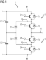
- FIG. 1 a three-point NPC inverter 1 according to the prior art is shown. For clarity, is in FIG. 1 as well as in the following FIGS. 2 to 6 only the circuit for one phase is shown. The described principles can be applied analogously to multiphase inverters.
- NPC neutral point clamped
- the in FIG. 1 illustrated three-point NPC inverter 1 comprises an upper half bridge 2 and a lower half bridge. 3
- the upper half-bridge 2 comprises a capacitor C1, a diode D1, two transistors T1, T2 and two drive circuits S1, S2 for the transistors T1, T2.
- the in FIG. 1 in the drawing level further upstream transistor T1 is an outer transistor T1 of the upper half-bridge 2.
- the lower half-bridge 3 comprises a capacitor C2, a diode D2, two transistors T3, T4 and two drive circuits S3, S4 for the transistors T3, T4.
- the in FIG. 1 in the drawing level further upstream transistor T3 is an inner transistor T3 of the lower half-bridge 3.
- the in FIG. 1 In the drawing plane further down transistor T4 is an outer transistor T4 of the lower half-bridge 3.
- the transistor T2 is switched off independently, without the transistor T1 having already been forcibly switched off. This can be avoided in the prior art by the transistor T2 provides feedback on its current switching state to the higher-level control logic, which then turns off the transistor T1 also. However, this feedback requires a potential separation, which causes costs. Moreover, the impermissible state still persists for a certain time.
- the invention has for its object to provide a three-point NPC power converter, which is protected in a cost effective manner against faulty commutation and avoids the above-mentioned disadvantages of the prior art.
- a three-point NPC power converter having an upper half-bridge and a lower half-bridge, each half-bridge each having an inner transistor and an outer transistor according to claim 1.
- the three-point NPC power converter is characterized in that the inner transistor of the upper half-bridge is formed cooperatively with the outer transistor of the upper half-bridge so that a signal indicative of a switching state of the inner transistor directly into a drive circuit for switching the outer transistor is coupled in and directly influenced a switching state of the outer transistor.
- An "immediate" coupling or influencing means that an action of the signal, which reflects the switching state of the inner transistor, takes place on the switching state of the outer transistor without any potential separation.
- the three-point NPC power converter according to the invention is distinguished from known solutions, in which the inner transistor provides feedback about its current switching state to a higher-order control logic. For this purpose, however, a potential separation is required, which causes costs.
- the previously-discussed impermissible states still persist for a short period of time.
- the three-point NPC power converter is characterized in that the inner transistor of the lower half-bridge is cooperatively formed with the outer transistor of the lower half-bridge so that a signal indicative of a switching state of the inner transistor directly into a drive circuit for switching the outer transistor is coupled in and directly influenced a switching state of the outer transistor.
- the drive circuit has a bridging element, which is designed to interrupt a direct influence on the switching state of the outer transistor by the signal, which reflects the switching state of the internal transistor, for a certain period of time.
- An “immediate” coupling or influencing means by analogy that an action of the signal, which reflects the switching state of the inner transistor, takes place on the switching state of the outer transistor without any potential separation.
- the three-point NPC power converter is characterized in that the upper half-bridge and the lower half-bridge are each configured as described above.
- the three-point NPC power converters according to the invention ensure that the previously-described prohibited switching states (a and b) do not occur with little effort.
- FIG. 2 For clarity, is in FIG. 2 as well as in the following FIGS. 3 to 6 only the circuit for one phase is shown.
- the described principles can be applied analogously to multiphase inverters.
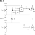
- FIG. 2 an upper half bridge 2 of a three-point NPC inverter 1 according to the invention is shown.
- the upper half bridge 2 comprises a diode D3, two transistors T1, T2 and two drive circuits S1, S2 for the Transistors T1, T2.
- the in FIG. 2 in the drawing level further upstream transistor T1 is an outer transistor T1 of the upper half-bridge 2.
- the in FIG. 2 In the drawing plane further down transistor T2 is an inner transistor T1 of the upper half-bridge 2.
- a signal which reflects the switching state of the internal transistor T2 is coupled into the drive circuit S1 of the external transistor T1.
- Potentials used refer to the potential POT2 in the drawing below.
- a voltage U 1 in the amount of 15 V In a difference of the potential P15T1 and the potential P0T1, which at The point B is applied, it is exemplified by a voltage U 2 in the amount of 15 V.
- the diode D3 connects the potential P15T2 with a logical AND operation 6, in which the drive circuit S1 is coupled. If the diode D3 is conducting, the logical AND operation 6 sends a signal 7 to the external transistor T1, so that it changes to a state "passing".
- the logical AND operation 6 is in a state that passes a signal from the drive circuit S1 as a signal 7 to the outer transistor T1.
- the three-point NPC converter it is possible on the one hand to prevent the outer transistor T1 from blocking before the inner transistor T2 has changed to the "blocking" state. In addition, it can be prevented that the outer transistor T1 is turned on, i. in the state "passing" changes before the internal transistor T2 has changed to the state "passing".
- the diode D3 must be designed to block at least one blocking voltage of the internal transistor T2.
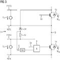
- FIG. 3 is a lower half-bridge 3 of a three-point NPC inverter 1 according to the invention shown.
- Potentials used refer to the potential POT4 in the drawing below.
- a difference between the potential P15T4 and the potential P0T4 is, for example, a voltage U 3 in the amount of 15 V.
- this is an example Voltage U 2 in the amount of 15 V.
- the lower half-bridge 3 comprises a diode D4, two transistors T3, T4 and two drive circuits S3, S4 for the transistors T3, T4.
- the in FIG. 3 in the drawing level further down transistor T4 is an outer transistor T4 of the lower half-bridge 3.
- the in FIG. 3 In the drawing plane above arranged transistor T3 is an inner transistor T3 of the lower half-bridge 3.
- a signal which reflects the switching state of the internal transistor T3 is coupled into the drive circuit S4 of the external transistor T4.
- a bridging element is provided, which is designed to interrupt an influencing of the switching state of the outer transistor T4 by the signal, which reflects the switching state of the internal transistor T3, for a certain period of time.
- the internal transistor T3 turns off, i. he goes into the state "blocking", for example, because of an interruption of its gate supply, the diode blocks D4.
- the potential at point C rises again to a higher value (for example 15 V). This corresponds to a logical zero of the logical AND operation 8, so that it does not forward a control command of the drive circuit S4 to the outer transistor T4.
- the diode D4 must usually be designed to block at least a double reverse voltage of the internal transistor T3 and the external transistor T4.
- a bridging element 9 is provided according to the invention, the function of which is based on FIG. 4 is explained.
- the bridging element 9 is in the present case a bypass switch 9.
- a bypass switch 9 in the function comparable components, such as a MOSFET or a bipolar transistor, or a corresponding logic circuit, as in FIG. 7 is shown to be used as a bridging element 9.
- the logical AND operation 8 is bridged by closing the bypass switch 9 in the case of a positive switching edge of a control signal of the drive circuit S4.
- FIG. 5 An associated waveform U A for the bypass switch 9 is in FIG. 5 shown. It shows FIG. 5 a normalized course of a first, second and third waveform U A1 for the bypass switch 9 and a normalized waveform S4 of the drive signal for the outer transistor T4 over time t.
- the according to the embodiment of the invention according to FIG. 4 relevant waveform is first waveform U A1 .
- the bypass switch 9 After a first (seen from the left side) positive switching edge of the drive signal S4, the bypass switch 9 must be switched on for a period of time T Ü . This ensures that the switching command of the drive signal S4 for the outer transistor T4, regardless of the potential applied at the point C, the transistor T4 turns on.
- the duration T Ü is to be chosen so long that the transistor T4 can safely reduce its reverse voltage within the period T Ü , so that the voltage across the transistor T4 voltage U T4 can fall below a certain value, for example below 5V.
- the transistor T3 is not protected against an overvoltage. If the transistor T3 switches off immediately after the first positive switching edge of the drive signal S4, then the transistor T3 is loaded with an inadmissibly high voltage. Therefore, the period of time T Ü is moreover to be selected so short that the transistor T3 can not be destroyed by the overvoltage during the period T Ü .
- a typical value for the duration TÜ is in the range of one microsecond.
- the transistor T4 After the expiration of the period T Ü , the transistor T4 has turned on and the potential C has fallen below a certain threshold, for example below 5V. Thus, the switching command of the drive circuit S4 is forwarded by the logical AND operation 8 to the transistor T4. In addition, after the time T Ü of the bypass switch 9 is opened for the remaining ON period of the transistor T4. Thus, the monitoring circuit according to the invention is active and the transistor T3 is effectively protected in case of faulty shutdown against a damaging overvoltage.
- the signals Ü A2 and Ü A3 in FIG. 5 represent examples of how the waveform for the bypass switch 9 can be particularly easily generated from the switching command signal of the drive circuit S4.
- the signal Ü A2 provides thereby an inverted and shifted by the period T Ü course of the signal of the drive circuit S4.
- the signal Ü A3 is an inverted form of the signal of the drive circuit S4, where only a negative edge of the signal Ü A3 by the time period T Ü is shifted in time.
- FIG. 6 shows a second embodiment of a lower half-bridge 3 of a three-point NPC inverter 1 according to the invention.
- Potentials used refer to the potential POT4 in the drawing below.
- a difference between the potential P15T4 and the potential P0T4 is, for example, a voltage U 3 in the amount of 15 V.
- this is an example Voltage U 2 in the amount of 15 V.
- FIG. 6 Similar to the first embodiment of the lower half-bridge 3, which is based on the Figures 3 and 4 includes in FIG. 6 shown lower half-bridge 3, a diode D4, two transistors T3, T4 and two drive circuits S3, S4 for the transistors T3, T4.
- transistor T4 is an outer transistor T4 of the lower half-bridge 3.
- transistor T3 is an inner transistor T3 of the lower half-bridge 3.
- the lower half-bridge 3 comprises a capacitor CÜ and a resistor RÜ, which are provided for acting on the bypass switch 9.
- the two components CÜ and RÜ in the in FIG. 6 arrangement shown within the lower half-bridge 3 are referred to herein as differentiators.
- the duration T Ü in which the logical AND gate 8 is bypassed, can be shortened by the provision of the capacitor CÜ and the resistor RÜ so far that it covers only a running time of a drive of the transistor T4 and not a complete duration of the switching edge of the transistor T4.
- a typical value for the duration T Ü in this case is 100 ns.
- the transistor T3 e.g. because the drive signal of the drive circuit S3 is delayed only slightly compared to the drive signal of the drive circuit S4 due to runtime tolerances, the potential at the point E decreases with the turn-on of the transistor T3 and the bypass switch 9 is closed again, so that the transistor T4 according to FIG the signal of the drive circuit S4 turns on. On the other hand, if the transistor T3 remains switched off, then the transistor T4 does not switch on independently of the signal of the drive circuit S4.
- the lower terminal of the resistor RÜ can be connected to other potentials relevant for driving the transistor T4 instead of the potential P15T4. This only causes an offset.
Landscapes
- Engineering & Computer Science (AREA)
- Power Engineering (AREA)
- Inverter Devices (AREA)
Priority Applications (5)
| Application Number | Priority Date | Filing Date | Title |
|---|---|---|---|
| EP18166543.1A EP3553936A1 (fr) | 2018-04-10 | 2018-04-10 | Agencement de circuit pour convertisseur à trois points |
| EP19716853.7A EP3776835B1 (fr) | 2018-04-10 | 2019-04-03 | Agencement de circuit pour convertisseur à trois points |
| CN201980024869.0A CN111989856B (zh) | 2018-04-10 | 2019-04-03 | 三点式变流器的电路布置 |
| PCT/EP2019/058370 WO2019197236A1 (fr) | 2018-04-10 | 2019-04-03 | Circuit pour convertisseur 3 points |
| US17/046,359 US11716031B2 (en) | 2018-04-10 | 2019-04-30 | Circuit assembly for neutral point clamped inverters that are protected from incorrect commutations |
Applications Claiming Priority (1)
| Application Number | Priority Date | Filing Date | Title |
|---|---|---|---|
| EP18166543.1A EP3553936A1 (fr) | 2018-04-10 | 2018-04-10 | Agencement de circuit pour convertisseur à trois points |
Publications (1)
| Publication Number | Publication Date |
|---|---|
| EP3553936A1 true EP3553936A1 (fr) | 2019-10-16 |
Family
ID=61971918
Family Applications (2)
| Application Number | Title | Priority Date | Filing Date |
|---|---|---|---|
| EP18166543.1A Withdrawn EP3553936A1 (fr) | 2018-04-10 | 2018-04-10 | Agencement de circuit pour convertisseur à trois points |
| EP19716853.7A Active EP3776835B1 (fr) | 2018-04-10 | 2019-04-03 | Agencement de circuit pour convertisseur à trois points |
Family Applications After (1)
| Application Number | Title | Priority Date | Filing Date |
|---|---|---|---|
| EP19716853.7A Active EP3776835B1 (fr) | 2018-04-10 | 2019-04-03 | Agencement de circuit pour convertisseur à trois points |
Country Status (4)
| Country | Link |
|---|---|
| US (1) | US11716031B2 (fr) |
| EP (2) | EP3553936A1 (fr) |
| CN (1) | CN111989856B (fr) |
| WO (1) | WO2019197236A1 (fr) |
Citations (4)
| Publication number | Priority date | Publication date | Assignee | Title |
|---|---|---|---|---|
| JP2002165462A (ja) * | 2000-11-20 | 2002-06-07 | Toshiba Corp | 半導体電力変換装置 |
| US20050281065A1 (en) * | 2004-06-22 | 2005-12-22 | Smc Electrical Products, Inc. | Inverter bridge controller implementing short-circuit protection scheme |
| DE102012205080A1 (de) * | 2012-03-29 | 2013-10-02 | Siemens Aktiengesellschaft | Umrichter und Verfahren zur Ansteuerung der Transistoren des Umrichters zum Schutz gegen unerlaubtes Einschalten |
| WO2015133985A1 (fr) * | 2014-03-03 | 2015-09-11 | Schneider Electric It Corporation | Systèmes et procédés permettant d'améliorer l'efficacité d'un onduleur fixé au point neutre |
Family Cites Families (5)
| Publication number | Priority date | Publication date | Assignee | Title |
|---|---|---|---|---|
| JP3102499B2 (ja) * | 1991-02-28 | 2000-10-23 | 株式会社東芝 | 中性点クランプ式電力変換器の制御装置 |
| JP4442348B2 (ja) * | 2004-07-22 | 2010-03-31 | 株式会社日立製作所 | 電力変換装置 |
| JP5324066B2 (ja) * | 2007-07-23 | 2013-10-23 | 東芝三菱電機産業システム株式会社 | 半導体電力変換装置 |
| CN202652100U (zh) * | 2012-06-07 | 2013-01-02 | 常熟开关制造有限公司(原常熟开关厂) | 一种二极管钳位式逆变桥结构 |
| US20150092467A1 (en) * | 2013-09-30 | 2015-04-02 | Infineon Technologies Ag | Driver Circuit for a Pair of Semiconductor Switches in a Leg of a Three-Level Inverter Half-Bridge |
-
2018
- 2018-04-10 EP EP18166543.1A patent/EP3553936A1/fr not_active Withdrawn
-
2019
- 2019-04-03 WO PCT/EP2019/058370 patent/WO2019197236A1/fr not_active Ceased
- 2019-04-03 CN CN201980024869.0A patent/CN111989856B/zh active Active
- 2019-04-03 EP EP19716853.7A patent/EP3776835B1/fr active Active
- 2019-04-30 US US17/046,359 patent/US11716031B2/en active Active
Patent Citations (4)
| Publication number | Priority date | Publication date | Assignee | Title |
|---|---|---|---|---|
| JP2002165462A (ja) * | 2000-11-20 | 2002-06-07 | Toshiba Corp | 半導体電力変換装置 |
| US20050281065A1 (en) * | 2004-06-22 | 2005-12-22 | Smc Electrical Products, Inc. | Inverter bridge controller implementing short-circuit protection scheme |
| DE102012205080A1 (de) * | 2012-03-29 | 2013-10-02 | Siemens Aktiengesellschaft | Umrichter und Verfahren zur Ansteuerung der Transistoren des Umrichters zum Schutz gegen unerlaubtes Einschalten |
| WO2015133985A1 (fr) * | 2014-03-03 | 2015-09-11 | Schneider Electric It Corporation | Systèmes et procédés permettant d'améliorer l'efficacité d'un onduleur fixé au point neutre |
Also Published As
| Publication number | Publication date |
|---|---|
| EP3776835B1 (fr) | 2023-09-27 |
| WO2019197236A1 (fr) | 2019-10-17 |
| CN111989856A (zh) | 2020-11-24 |
| US20210257926A1 (en) | 2021-08-19 |
| EP3776835A1 (fr) | 2021-02-17 |
| CN111989856B (zh) | 2024-05-14 |
| US11716031B2 (en) | 2023-08-01 |
Similar Documents
| Publication | Publication Date | Title |
|---|---|---|
| DE10020981B4 (de) | Motor-Steuergerät mit Fehlerschutzschaltung | |
| EP3151405B1 (fr) | Circuit d'équilibrage des tensions aux bornes des condensateurs d'un circuit intermédiaire à courant continu | |
| EP0060331A1 (fr) | Dispositif de protection contre court-circuit pour un régulateur de courant continu | |
| EP1756926A1 (fr) | Procede de traitement de defaut dans un circuit convertisseur pour la commutation de trois niveaux de tension | |
| DE102015120166B3 (de) | Steuereinrichtung für einen Leistungshalbleiterschalter | |
| DE102004057187A1 (de) | Inverterschaltung | |
| EP2342824B1 (fr) | Circuit en demi-pont protégé contre les courts-circuits avec commutateurs semiconducteurs | |
| DE102021122687A1 (de) | Anordnung und Verfahren zur Entladung eines Zwischenkreiskondensators | |
| DE102015110513B3 (de) | Leistungshalbleiterschaltung mit einem Feldeffekttransistor | |
| DE102011078899A1 (de) | Transistor-Halbbrückensteuerung | |
| DE102012102220B4 (de) | Sicherheitsschaltung und Sicherheitsschaltgerät mit einer Sicherheitsschaltung | |
| DE3905645C2 (fr) | ||
| WO2002001694A2 (fr) | Circuit electronique pour appareil d'alimentation en energie, notamment pour chargeur de batteries | |
| DE19928856C2 (de) | Schaltungsanordnung zum Überlastungsschutz | |
| EP0013710A1 (fr) | Amplificateur d'attaque symétrique dont la sortie peut être reliée directement aux sorties d'autres amplificateurs d'attaque | |
| EP3895312B1 (fr) | Commutateur électronique à régulation du courant | |
| EP3776835B1 (fr) | Agencement de circuit pour convertisseur à trois points | |
| EP1468435A1 (fr) | Circuit electrique muni d'un relais electromagnetique et d'un systeme de couplage monte de maniere parallele a un contact du relais electromagnetique | |
| DE102010015095A1 (de) | Treiberschaltung für eine Last und Baugruppe aus Treiberschaltung und einer Last | |
| DE102004013108B4 (de) | Verfahren zum Betreiben einer Versorgungseinheit für eine Treiberschaltung sowie Versorgungseinheit für eine Treiberschaltung | |
| EP2269296B1 (fr) | Circuit de controle pour un moteur a courant continu avec un pont en h et un circuit de frein moteur | |
| WO2021239173A1 (fr) | Système de circuit électrique et système d'entraînement pour entraîner un véhicule automobile | |
| DE4428115A1 (de) | Steuergerät mit einer Schaltungsanordnung zum Schutz des Steuergerätes bei Unterbrechung der Steuergerätemasse | |
| DE102010046539A1 (de) | Schaltungsanordnung zum Betrieb einer Kaskodenschaltung | |
| WO1999009652A1 (fr) | Circuit de commutation de charges |
Legal Events
| Date | Code | Title | Description |
|---|---|---|---|
| PUAI | Public reference made under article 153(3) epc to a published international application that has entered the european phase |
Free format text: ORIGINAL CODE: 0009012 |
|
| AK | Designated contracting states |
Kind code of ref document: A1 Designated state(s): AL AT BE BG CH CY CZ DE DK EE ES FI FR GB GR HR HU IE IS IT LI LT LU LV MC MK MT NL NO PL PT RO RS SE SI SK SM TR |
|
| AX | Request for extension of the european patent |
Extension state: BA ME |
|
| STAA | Information on the status of an ep patent application or granted ep patent |
Free format text: STATUS: THE APPLICATION IS DEEMED TO BE WITHDRAWN |
|
| 18D | Application deemed to be withdrawn |
Effective date: 20200603 |