EP3555953B1 - Verfahren zum entwurf von schlitzantennen für elektronische wearable-vorrichtungen und leitfähige gehäuse - Google Patents
Verfahren zum entwurf von schlitzantennen für elektronische wearable-vorrichtungen und leitfähige gehäuse Download PDFInfo
- Publication number
- EP3555953B1 EP3555953B1 EP17882182.3A EP17882182A EP3555953B1 EP 3555953 B1 EP3555953 B1 EP 3555953B1 EP 17882182 A EP17882182 A EP 17882182A EP 3555953 B1 EP3555953 B1 EP 3555953B1
- Authority
- EP
- European Patent Office
- Prior art keywords
- antenna
- conductive
- bracket
- slot antenna
- metal
- Prior art date
- Legal status (The legal status is an assumption and is not a legal conclusion. Google has not performed a legal analysis and makes no representation as to the accuracy of the status listed.)
- Active
Links
Images









Classifications
-
- H—ELECTRICITY
- H01—ELECTRIC ELEMENTS
- H01Q—ANTENNAS, i.e. RADIO AERIALS
- H01Q1/00—Details of, or arrangements associated with, antennas
- H01Q1/27—Adaptation for use in or on movable bodies
- H01Q1/273—Adaptation for carrying or wearing by persons or animals
-
- H—ELECTRICITY
- H01—ELECTRIC ELEMENTS
- H01Q—ANTENNAS, i.e. RADIO AERIALS
- H01Q1/00—Details of, or arrangements associated with, antennas
- H01Q1/12—Supports; Mounting means
- H01Q1/22—Supports; Mounting means by structural association with other equipment or articles
-
- H—ELECTRICITY
- H01—ELECTRIC ELEMENTS
- H01Q—ANTENNAS, i.e. RADIO AERIALS
- H01Q1/00—Details of, or arrangements associated with, antennas
- H01Q1/12—Supports; Mounting means
- H01Q1/22—Supports; Mounting means by structural association with other equipment or articles
- H01Q1/2258—Supports; Mounting means by structural association with other equipment or articles used with computer equipment
- H01Q1/2266—Supports; Mounting means by structural association with other equipment or articles used with computer equipment disposed inside the computer
-
- H—ELECTRICITY
- H01—ELECTRIC ELEMENTS
- H01Q—ANTENNAS, i.e. RADIO AERIALS
- H01Q1/00—Details of, or arrangements associated with, antennas
- H01Q1/27—Adaptation for use in or on movable bodies
-
- H—ELECTRICITY
- H01—ELECTRIC ELEMENTS
- H01Q—ANTENNAS, i.e. RADIO AERIALS
- H01Q1/00—Details of, or arrangements associated with, antennas
- H01Q1/36—Structural form of radiating elements, e.g. cone, spiral, umbrella; Particular materials used therewith
- H01Q1/38—Structural form of radiating elements, e.g. cone, spiral, umbrella; Particular materials used therewith formed by a conductive layer on an insulating support
-
- H—ELECTRICITY
- H01—ELECTRIC ELEMENTS
- H01Q—ANTENNAS, i.e. RADIO AERIALS
- H01Q1/00—Details of, or arrangements associated with, antennas
- H01Q1/44—Details of, or arrangements associated with, antennas using equipment having another main function to serve additionally as an antenna, e.g. means for giving an antenna an aesthetic aspect
-
- H—ELECTRICITY
- H01—ELECTRIC ELEMENTS
- H01Q—ANTENNAS, i.e. RADIO AERIALS
- H01Q13/00—Waveguide horns or mouths; Slot antennas; Leaky-waveguide antennas; Equivalent structures causing radiation along the transmission path of a guided wave
- H01Q13/10—Resonant slot antennas
-
- H—ELECTRICITY
- H01—ELECTRIC ELEMENTS
- H01Q—ANTENNAS, i.e. RADIO AERIALS
- H01Q13/00—Waveguide horns or mouths; Slot antennas; Leaky-waveguide antennas; Equivalent structures causing radiation along the transmission path of a guided wave
- H01Q13/10—Resonant slot antennas
- H01Q13/18—Resonant slot antennas the slot being backed by, or formed in boundary wall of, a resonant cavity ; Open cavity antennas
-
- H—ELECTRICITY
- H02—GENERATION; CONVERSION OR DISTRIBUTION OF ELECTRIC POWER
- H02J—ELECTRIC POWER NETWORKS; CIRCUIT ARRANGEMENTS OR SYSTEMS FOR SUPPLYING OR DISTRIBUTING ELECTRIC POWER; SYSTEMS FOR STORING ELECTRIC ENERGY
- H02J7/00—Circuit arrangements for charging or discharging batteries or for supplying loads from batteries
- H02J7/02—Circuit arrangements for charging or discharging batteries or for supplying loads from batteries for charging batteries from AC mains by converters
-
- H—ELECTRICITY
- H01—ELECTRIC ELEMENTS
- H01Q—ANTENNAS, i.e. RADIO AERIALS
- H01Q1/00—Details of, or arrangements associated with, antennas
- H01Q1/12—Supports; Mounting means
- H01Q1/22—Supports; Mounting means by structural association with other equipment or articles
- H01Q1/24—Supports; Mounting means by structural association with other equipment or articles with receiving set
- H01Q1/241—Supports; Mounting means by structural association with other equipment or articles with receiving set used in mobile communications, e.g. GSM
- H01Q1/242—Supports; Mounting means by structural association with other equipment or articles with receiving set used in mobile communications, e.g. GSM specially adapted for hand-held use
- H01Q1/243—Supports; Mounting means by structural association with other equipment or articles with receiving set used in mobile communications, e.g. GSM specially adapted for hand-held use with built-in antennas
-
- H—ELECTRICITY
- H01—ELECTRIC ELEMENTS
- H01Q—ANTENNAS, i.e. RADIO AERIALS
- H01Q1/00—Details of, or arrangements associated with, antennas
- H01Q1/48—Earthing means; Earth screens; Counterpoises
Definitions
- Modern electronic devices frequently include one or more radio-frequency antennas to facilitate wireless communication with other electronic devices.
- the antennas may be configured to fit within a restricted envelope while still providing desirable emission and reception characteristics.
- Some antenna designs exert an upward or outward force on the display window, causing the display window to separate from the metal housing over time, which may cause the device to become no longer water resistant and/or swim proof. Finally, some antenna designs may be undesirably mechanically complex and/or costly. Accordingly, disclosed herein are embodiments of wearable devices and biometric monitoring devices having a monopole-excited slot antenna design that addresses one or more of the above issues.
- the disclosed antenna architectures include two portions.
- the antenna architectures include a monopole antenna having a monopole radiator on a plastic carrier implemented at a top of a display area within a metal housing of the device.
- the monopole radiator is connected through an antenna clip on a printed circuit board (PCB) to a radio frequency (RF) engine.
- the monopole antenna can be implemented as a flex film antenna radiator assembled on, for example, a plastic carrier.
- the monopole radiator can generate electromagnetic fields to induce the slot antenna to transmit or receive radio frequency signals.
- the antenna can be designed to be particularly receptive to (or emissive of) radio frequency energy at frequencies within the frequency band(s) for the wireless communications protocol(s) that the antenna is designed to support, and the antenna can also be designed to not be particularly receptive to (or emissive of) radio frequency energy at frequencies outside of the frequency band(s).
- Antennas may achieve such selectivity by virtue of their physical geometry and the dimensions that define that geometry.
- the monopole antenna portion can be tuned to have a certain length and a matching circuit on the PCB may be utilized to tune the antenna impedance to achieve targeted performance characteristics.
- the metal plate and/or metal housing can be conductive.
- the metal plate and/or metal housing can include one or more materials that include a conductivity of 1E5 Siemens/m and/or higher.
- the disclosed monopole-excited slot antennas reduce the dead band of the display window or provide a desirably or advantageously small dead band at a top of the display window.
- the monopole antenna component that excites the slot antenna can provide a targeted excitation for the slot antenna with a reduced distance between a top side of the metal housing and a display module relative to a pure monopole antenna or inverted-F antenna (IFA) architecture with similar antenna performance.
- IFA inverted-F antenna
- the disclosed monopole-excited slot antennas accommodate a device architecture having a printed circuit board (PCB) mounted close to the bottom of a metal housing.
- PCB printed circuit board
- the PCB may require the PCB to be mounted above the battery to achieve suitable performance, manufacturing costs, and/or mechanical complexity.
- the battery size is reduced relative to devices that incorporate the antenna architectures disclosed herein that allow the battery to be placed above the PCB.
- the disclosed monopole-excited slot antennas function by using a capacitively-coupled monopole antenna radiator to excite an antenna slot.
- the disclosed antenna design may be advantageous due at least in part to being mechanically simpler (e.g., not requiring the using of a coaxial cable or other transmission line from the PCB to the antenna) resulting in a lower cost and increased ease of manufacture.
- the various implementations discussed herein may be used, for example, to provide a monopole-excited slot antenna that provides BLUETOOTH ® functionality, including BLUETOOTH Low Energy (Bluetooth LE or BTLE) functionality.
- BLUETOOTH ® functionality including BLUETOOTH Low Energy (Bluetooth LE or BTLE) functionality.
- BLUETOOTH Low Energy Bluetooth LE or BTLE
- Such a compact and efficient antenna may be of particular use in highly-integrated devices having a small form factor.
- the disclosed antennas can be used in biometric monitoring devices, e.g., wearable devices that track, report, and communicate various biometric measurements, e.g., distance traveled, steps taken, flights of stairs climbed, etc.
- biometric monitoring devices e.g., wearable devices that track, report, and communicate various biometric measurements, e.g., distance traveled, steps taken, flights of stairs climbed, etc.
- Such devices may take the form of a small device that is clipped to a person'
- Such a device may, for example, contain various processors, printed circuit boards, sensors, triaxial accelerometers, triaxial gyroscopes, an altimeter, a display, a vibramotor, a rechargeable battery, a recharging connector, and an input button all within a metal housing that measures approximately between 1.62" and 2" in length, 0.75" and 0.85" in width, and 0.3" and 0.44" in thickness.
- a monopole-excited slot antenna may be used in such a device to provide RF communication in a water resistant and/or swim-proof wearable device, to reduce the dead band of a display window, and/or to provide a more cost-efficient and mechanically simple device.
- monopole-excited slot antennas may provide the ability to offer a more compact communications solution than might otherwise be possible, allowing additional volume within the metal housing to be made available for other purposes, such as a larger battery.
- Such dimensions may prove to be particularly well-suited to RF communications in the BLUETOOTH ® wireless protocol bands, e.g., 2402 MHz to 2480 MHz.
- Monopole-excited slot antenna antennas that support other wireless communications protocols may also be designed using the principles outlined herein.
- the disclosed antenna architectures may be configured or dimensioned to be suitable for use with wireless networks and radio technologies, such as wireless wide area network (WWAN) (e.g., cellular) and/or wireless local area network (WLAN) carriers.
- WWAN wireless wide area network
- WLAN wireless local area network
- wireless networks and radio technologies include but are not limited to Long Term Evolution (LTE) frequency bands or other cellular communications protocol bands, GPS (Global Positioning System) or GNSS (Global Navigation Satellite System) frequency bands, ANT TM , 802.11, and ZigBee TM , for example, as well as frequency bands associated with other communications standards.
- LTE Long Term Evolution
- GPS Global Positioning System
- GNSS Global Navigation Satellite System
- ANT TM TM
- 802.11 Global Navigation Satellite System
- ZigBee TM ZigBee TM
- biometric monitoring device is used herein according to its broad and ordinary meaning, and may be used in various contexts herein to refer to any type of biometric tracking devices, personal health monitoring devices, portable monitoring devices, portable biometric monitoring devices, or the like.
- biometric monitoring devices in accordance with the present disclosure may be wearable devices, such as may be designed to be worn (e.g., continuously) by a person (i.e., "user,” “wearer,” etc.). When worn, such biometric monitoring devices may be configured to gather data regarding activities performed by the wearer, or regarding the wearer's physiological state.
- Such data may include data representative of the ambient environment around the wearer or the wearer's interaction with the environment.
- the data may comprise motion data regarding the wearer's movements, ambient light, ambient noise, air quality, etc., and/or physiological data obtained by measuring various physiological characteristics of the wearer, such as heart rate, perspiration levels, and the like.
- a biometric monitoring device may leverage other devices external to the biometric monitoring device, such as an external heart rate monitor in the form of an EKG sensor for obtaining heart rate data, or a GPS or GNSS receiver in a smartphone may be used to obtain position data, for example.
- the biometric monitoring device may communicate with these external devices using wired or wireless communications connections.
- the concepts disclosed and discussed herein may be applied to both stand-alone biometric monitoring devices as well as biometric monitoring devices that leverage sensors or functionality provided in external devices, e.g., external sensors, sensors or functionality provided by smartphones, etc.
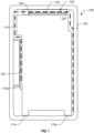
- FIG. 1 illustrates a top view of an example wearable electronic device 100 having a metal plate 110 within a metal housing 105 forming a slot antenna 115 that is excited by a monopole antenna 120.
- the housing (such as a metal housing) 105 may be designed to accommodate a display that will be worn on a person's wrist.
- a wristband (not shown) may be connected to the opposing ends of the metal housing 105, and the completed unit may be worn on someone's wrist.
- the metal housing 105 may be designed to conform better to the cross-sectional curvature of a person's forearm and the interior of the metal housing may be occupied by various electrical components, including a PCB or FPCB (Flexible Printed Circuit Board) that includes, for example, various sensors, processors, power management components, etc.
- the metal housing 105 may include additional features, such as a metal button bracket 107, to support other elements within the metal housing 105.
- the slot antenna 115 is structured as a gap between the metal plate 110 and the metal housing 105 (including the metal button bracket 107) stopped at two ends with grounding contacts 112a, 112b between the metal plate 110 and the metal housing 105.
- the slot antenna 115 can be configured as a half-wavelength slot antenna (e.g., a length of about 6.25 cm for BLUETOOTH ® communication).
- the slot antenna 115 is not directly driven by any element (e.g., an antenna feed or coaxial cable) coupled to the printed circuit board or other similar component.
- the monopole antenna 120 is designed to excite the slot antenna 115 in a targeted mode.
- the monopole antenna 120 includes a flex antenna as the monopole radiator 124 on a monopole antenna carrier 122 made of a plastic mechanical component.
- the flex antenna 124 is assembled on the surface of the carrier 122 and the carrier 122 is placed inside the metal housing 105.
- the carrier 122 can be attached to the metal housing 105 or other component of the device 100.
- the device 100 includes a display window 130 mechanically coupled to the metal housing 105.
- the display window 130 and the metal housing 105 form a sealed enclosure that is water resistant and/or swim proof.
- the device 100 includes a touch module 132 and a display module 134.
- the touch module 132 is configured to detect touch input on the display window 130.
- the display module 134 is configured to display images or information through the display window 130.
- the component layer 141 can include microprocessors, RAM (random access memory), ROM (read only memory), ASICs (application specific integrated circuit), FPGAs (field programmable gate array), surface mounted elements, integrated circuits, and the like.
- the PCB 140 provides electrical components and circuitry that directs and interprets electrical signals for the device 100.
- the PCB 140 is electrically coupled to the display and touch modules 132, 134 to interpret touch input and to provide images or information to display.
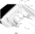
- the PCB 140 is coupled to an antenna feed clip 142 that is electrically coupled to the monopole antenna 120.
- the PCB 140 can include a ground plane area 140a that forms a ground plane for the monopole antenna 120.
- the PCB 140 can include a feed clip area 140b that does not include conductive elements other than where the antenna feed clip 142 is mounted on and electrically coupled to the PCB 140.
- the PCB 140 can include a trace that electrically couples the ground plane area 140a to the feed clip area 140b, the feed clip 142 being electrically coupled to the trace in the feed clip area 140b.
- the ground plane for the monopole antenna 120 may be provided by a large metalized area, conductive traces in a printed circuit board (e.g., the PCB 140) or flexible printed circuit board, a metal plate and/or surface within the metal housing 105, etc.
- the device 100 can also include a vibrating motor 143 to provide haptic feedback or to otherwise mechanically vibrate the device 100.
- the PCB 140 can be grounded to the metal housing 105 through one or more grounding screws that electrically couple the PCB 140 to the metal housing 105.
- the battery 135 can be about 0.05 mm below the metal plate 110.
- a layer of a non-conductive, low RF loss, rigid material may be inserted to fit in the 0.05 mm gap to attach or otherwise mechanically couple the metal plate 110 to the battery 135.
- the battery 135 is between about 0.01 mm and about 0.1 mm below the metal plate 110, between about 0.03 mm and about 0.7 mm below the metal plate 110, or between about 0.04 mm and about 0.06 mm below the metal plate 110.
- the battery 135 can be about 0.48 mm above the component layer 141. In some embodiments, the battery 135 is between about 0.4 mm and about 0.6 mm above the component layer 141, between about 0.42 mm and about 0.55 mm above the component layer 141, or between about 0.45 mm and about 0.5 mm above component layer 141. In some embodiments, as described herein, a plastic bracket can be placed in this gap to support the battery 135 above the component layer 141 of the PCB 140.
- a plastic bracket can be placed in this gap to support the battery 135 above the component layer 141 of the PCB 140.
- the battery 135 can be about 0.53 mm from the right side of the metal housing 105 (e.g., as shown in FIG. 3 ). In some embodiments, the battery 135 is between about 0.4 mm and about 0.6 mm from the right side of the metal housing 105, between about 0.45 mm and about 0.58 mm from the right side of the metal housing 105, or between about 0.5 mm and about 0.55 mm from the right side of the metal housing 105.
- the battery 135 can be about 3.2 mm thick. In some embodiments, the battery 135 can be between about 2.5 mm and about 4 mm thick, between about 2.75 mm and about 3.75 mm thick, or between about 3 mm and about 3.5 mm thick. Although particular values for certain device geometries have been provided, it is to be understood that these dimensions can be changed relative to the size of the metal housing 105.
- the disclosed monopole-excited slot antenna configurations provide a number of advantages, especially when implemented in wearable devices such as biometric monitoring devices. To illustrate one or more advantages, comparison can be made to other antenna configurations. For example, a device having a single monopole or IFA (inverted "F" antenna) antenna design can achieve similar performance by increasing the dead band at the top of the display window. This is undesirable as it detracts from the design and utility of the device. Accordingly, the disclosed antenna design provides reduced dead bands relative to monopole or IFA antenna configurations that provide comparable antenna performance (e.g., transmission and reception strength). In some embodiments, the slot antenna is not directly excited by an antenna feed physically coupled to the PCB.
- IFA inverted "F” antenna
- Another alternative configuration includes a slot antenna that is directly fed from the PCB rather than being coupled to a monopole antenna, with the PCB being placed above the battery. In devices with tapered cross-sections, this may undesirably reduce the size of the battery.
- Another alternative configuration includes a slot antenna that is directly fed from the PCB rather than being coupled to a monopole antenna, with the PCB below the battery.
- a feed line e.g., coaxial cable
- Using a coaxial cable complicates the mechanical implementation and increases the cost of the device.
- the disclosed antenna architectures can be configured to achieve similar performance characteristics as an elevated feed design using a coaxial cable.
- Another alternative configuration includes a monopole or IFA antenna outside the metal housing 105.
- the antenna feed would typically connect the PCB inside the metal housing 105 to the antenna located outside the metal housing 105. Accordingly, the disclosed antenna architectures can be housed entirely within the metal housing 105 to facilitate water resistance of the device 100.
- FIG. 5 illustrates a top view of the wearable electronic device 100 of FIG. 1 with an NFC antenna 145 on top of the metal plate 110.
- the monopole-excited slot antenna 114 can be configured to operate in a way that allows the NFC antenna 145 to continue to operate and may operate with comparable performance.
- the NFC antenna 145 can be about 25.6 mm ⁇ 12.8 mm.
- the NFC antenna 145 can be positioned about 1 mm from the slot antenna 115.
- the device 100 can also include a first flex cable 144a configured to couple to one or more modules (e.g., the touch module 132 or the display module 134) and a second flex cable 144b configured to couple to the battery 135 and/or to the NFC antenna 145.
- the number of flex cables can vary and may be at least 1 flex cable, at least 2 flex cables, at least 3 flex cables, and so forth. It is also to be understood that one or more of the flex cables may be replaced with one or more wires. For example, wires can couple to the battery 135 and/or the NFC antenna 145.
- FIG. 6 illustrates a top view of the wearable electronic device 100 of FIG. 1 with a display module 134 and a touch module 132 shown on top of the metal plate 110 to illustrate a dead band of the display window with the disclosed antenna configuration.
- the dead band of the display is considered to be the non-active area of the display window or where the display module 134 does not display information through the display window. Accordingly, as illustrated in FIG. 6 , the dead band of the display window extends from an edge of the display window (shown here as coinciding with an exterior edge of the metal housing 105) to a point beyond the edge of the display module 134. It should be understood that the display window can extend beyond the metal housing 105 or it can be configured to not extend to the edge of the metal housing 105.
- the distance from the edge of the display module 134 to an active region of the display module 134 contributes to the dead band of the display window and can be about 1 mm in length.
- the RF signal from the slot antenna 115 is radiated through the gap between the metal housing 105 and the edges of the display module 134 and the touch module 132.
- the monopole antenna 120 has a clearance at the top of the device 100 of about 2 mm from the interior of the metal housing 105 to the edge of the display module 134, contributing about 2 mm to the total dead band.
- the contribution to the dead band, or the increase in the dead band relative to a device where the display module is flush with an interior wall of the metal housing 105 can be between about 1 mm and about 3 mm, between about 1.5 mm and about 2.5 mm, or between about 1.75 mm and about 2.25 mm.
- the dead band of the display window can be less than or equal to about 6 mm, less than or equal to about 5 mm, less than or equal to about 4.5 mm, or less than or equal to about 4 mm.
- the dead band of the display overlaps with the dead band of the monopole antenna.
- the dead band of the display and the dead band of the monopole antenna include a space between an interior surface of the metal housing 105 and an edge of the metal plate 110.
- an alternative antenna design is to include a monopole, IFA, or loop antenna placed at the top of the display area.
- simulations indicate that the contribution to the dead band of the display window by the antenna would have to be increased to about 4.8 mm from about 2 mm.
- the disclosed antenna architectures provide desirable or advantageous performance with a relatively small dead band compared to a pure monopole, IFA, or loop antenna implementation.
- the antenna matching circuit can be configured to connect the feed clip 142 to an RF engine chipset on the PCB 140.
- the feed clip 142 may also be provided by structures other than that shown, e.g., by a bonded wire, spring contact pin, a combination of such features or other features that provide for electrically-conductive contact between the monopole radiator and the printed circuit board.
- the monopole radiator 124 is routed in a clockwise pattern for efficient excitation of the slot antenna mode as seen in FIG. 7 . In certain embodiments, the monopole radiator 124 performs better when placed closer to the display window (not shown).
- technologies that can be used to implement the monopole antenna 120 including, but not limited to, laser designated structure (LDS), 2-shot plated, stamped sheet metal, printed antenna, and the like.
- the PCB 140 can be grounded to the metal housing 105 at grounding points, e.g., grounding screws.
- copper layers can be removed from the PCB 140 to improve performance by reducing the capacitive coupling between the PCB and the metal housing 105.
- FIGS. 10A-10B illustrate another example embodiment of a metal bracket 1010 configured to form a slot antenna within a metal housing.
- the metal bracket 1010 can include a metal frame with vertical walls 1013 configured to contain or secure the battery in place and/or to control the radiating slot width.
- the metal bracket 1010 includes a main plate 1011 and side walls 1013 with grounding clips 1012a, 1012b, 1014.
- a thin dielectric spacer can also be used at both side gaps between the metal housing side wall and the metal bracket 1010 to control the variation in radiating slot width.
- the dielectric spacer can be a well-controlled material that is non-conducting, low RF loss, rigid, and capable of holding its thickness.
- a plastic film with controlled thickness can be used with a pressure or spring fit to control spacing.
- tape can be used with the metal bracket 1010 with spring fingers to control spacing.
- FIG. 11 illustrates a cross-section of an example wearable electronic device 1100 having a metal bracket 1110 configured similarly to the metal bracket 1010 of FIGS. 10A-10B .
- the device 1100 is similar to the device 100 described herein with reference to FIGS. 1-9 , except that the metal plate 1110 includes side walls that extend along the sides of the battery 135 to control the gap width of the slot antenna 1115.
- FIG. 12A illustrates an example plastic bracket 1250 to secure the battery in place within a metal housing.
- the plastic bracket 1250 can be positioned between the battery 135 and the component layer of the PCB 141.
- the plastic bracket 1250 can be made of a polycarbonate plastic or other similar material.
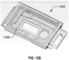
- FIG. 12B illustrates an example metal housing 1305 of a wearable electronic device with a slot antenna as described herein.
- the cavity formed by the metal housing 1305 can provide a volume for components of the electronic device. Generally, the larger the cavity volume, the better antenna efficiency is expected. However, smaller devices may be generally preferred for particular applications, such as biometric monitoring devices for use during fitness activities.
- the surfaces 1306 of the metal housing 1305 capacitively couple to the battery and other PCB components. It is advantageous to use one or more features described herein to control the spacing of the components with respect to the metal housing 1305 to avoid undesired RF shorts.
- FIGS. 13A , 13B , and 13C illustrate simulation results for an example excited slot antenna for wearable electronic device.
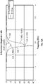
- FIG. 13A illustrates simulation results for S-parameter, S11, over frequency for configurations including a matching circuit and raw antenna impedance (e.g. excluding the matching circuit). Simulation results indicate that this design would achieve S11 better than -15 dB in the BLUETOOTH ® 2.4GHz frequency band.
- FIG. 13B illustrates the simulated antenna impedance in a smith chart of the raw antenna (e.g. no matching circuit) and the antenna with the matching circuit included.
- FIG. 13C illustrates the simulated antenna radiation pattern which has a main beam whose direction is perpendicular to the display window 130 of the wearable electronic device.
- the metal housing 105 shields the user's wrist from the antenna and reduces the electromagnetic energy that is radiated in toward the user's wrist. The antenna impedance and antenna efficiency were observed to change minimally between free space and wrist worn user cases.
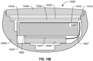
- FIGS. 14A and 14B respectively illustrate a top view and a cross-section along the width of another example wearable electronic device 1400 having a metal plate 1410 within a metal housing 1405 forming a slot antenna 1415 that is excited by a direct feed 1447 from a printed circuit board 1440.
- the direct feed 1447 can be implemented using a coaxial cable or other transmission line to elevate the feed 1447 from the PCB 1440 to the metal plate 1410.
- the feed 1447 can include two or more wires or electrical conductors, one (e.g. the RF feed) being coupled to the metal plate 1410 and the other (e.g. ground) being coupled to the metal housing 1405.
- the feed 1447 is a coaxial cable with the outer conductor (e.g., braided shield) being electrically coupled to the metal plate 1410 and the inner conductor being electrically coupled to the metal housing 1405.
- the metal plate 1410 can include two or more grounding pins or grounding connections that electrically couple the metal plate 1410 to the metal housing 1405 at targeted locations to define the length of the slot antenna 1415 and/or to improve performance (e.g., by reducing undesired resonances in the metal plate 1410).
- the back cavity (and/or the dielectric gap) 1460 can be an area below the battery 1435 and above the PCB 1440 and component layer of the PCB 1441.
- the metal plate 1410 near the display window 1430 of the device 1400.
- the direct feed 1447 allows the metal plate 1410 to be positioned high within the metal housing 1405 while still allowing the PCB 1440 to be placed below the battery 1435. This advantageously allows the battery 1435 to be larger than configurations where the PCB 1440 is above the battery 1435.
- the slot antenna 1415 with direct feed 1447 may increase complexity and cost relative to the monopole-excited slot antennas described herein, the device 1400 can provide similar RF communication performance while providing similar advantages to the monopole-excited slot antenna architecture, such as reduced dead band and water resistance.
- the metal bracket can enclose at least a portion of the battery.
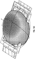
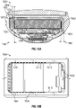
- FIGS 15A, 15B , 15C, and 15D respectively illustrate a cross-section along the width, top view, a perspective view, and cross-section along the length of another example wearable electronic device 1500 having a metal bracket 1504 within a metal housing 1512 forming a slot antenna 1513 that can be excited by a monopole antenna 1510.
- the metal housing 1512 can be designed to be worn on a person's wrist.
- the slot antenna 1513 can extend from a grounding point (e.g. a clip ground) 1514 to another grounding point (e.g. a screw ground) 1518.
- An additional grounding point 1516 can be used to eliminate unwanted resonances.
- the monopole antenna 1510 can excite the slot antenna 1513, for example, by electromagnetic field coupling.
- the slot antenna architecture includes a printed circuit board ("PCB") mounted close to the bottom of a metal housing.
- a battery can be disposed above the PCB and within the metal housing.
- the antenna slot can be excited by a capacitive coupled monopole antenna radiator.
- the monopole antenna 1510 can be placed on a plastic carrier.
- spring force to the cover glass window can be reduced and/or eliminated which can provide benefits for water resistant features.
- the monopole antenna 1510 can comprise a laser direct structuring antenna that can be disposed on a plastic carrier.
- the monopole antenna 1510 can be disposed in the dead band at the top of the display area inside the metal housing 1512.
- the monopole antenna 1510 can be connected through an antenna clip placed on a PCB to the radio frequency engine.
- the metal bracket 1504 is inserted molded into the plastic carrier for the monopole antenna 1510.
- the metal bracket 1504 at least partially surrounds the battery 1502.
- the battery 1502 can be disposed inside the surroundings of a metal bracket 1504.
- the display module can be disposed above the battery 1502.
- An NFC flex antenna can be placed on top of the battery 1502 or below the display module.
- a PCB can be placed below the metal plate 1504.
- the metal bracket 1504 can be disposed at least partially below battery 1502.
- the metal bracket 1504 can be disposed such that the slot gaps between the metal bracket 1504 and the metal housing 1512, and such that the back cavity gap 1568 between the metal bracket 1504 and PCB may not be affected by the size and/or swelling of the battery 1502.
- the metal bracket 1504 can be disposed on the bottom surface of the battery 1502 and extend vertically to be adjacent to at least a portion of the side walls of the battery 1502.
- the slot gaps 1560, 1558, 1562, and 1564 and back cavities 1566 and 1568 can provide channels for slot antenna to radiate signals through, and as such, the effect of battery tolerance to antenna performance can be reduced and/or eliminated based on the structural design of the metal bracket 1504 and the battery 1502.
- the back cavities 1566 and 1568 can be areas below the metal bracket 1504 and above the PCB or the metal housing 1512 where antenna electromagnetic fields resonate.
- the back cavities 1566 and 1568 can be sensitive areas for a slot antenna design in a metal enclosure.
- such structural design can improve isolation of the metal housing 1512, the PCB, and/or the metal bracket 1504 with the back cavities 1566 and 1568. This becomes important because the electromagnetic field inside the back cavities can affect antenna performance if a metal component is disposed inside the back cavities.
- a frequency tuning mechanism is provided.
- the frequency tuning mechanism can provide tuning of the antenna without requiring mechanical changes to the size and/or structure of the device design.
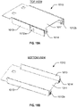
- FIGS. 16A and 16B respectively illustrate metal brackets to facilitate antenna frequency tuning.
- FIG. 16A illustrates metal brackets with an eight-tab structure.
- FIG. 16B illustrates metal brackets with a zero-tab structure.
- a wearable device includes a slot antenna that can be excited by a monopole antenna.
- the length of the slot antenna can follow a path within the wearable device.
- the length of the slot antenna can follow a line that goes around eight metal tab structures.
- the metal tab structure(s) can provide frequency tuning with a certain resolution.
- Each of the teeth or tabs (or combination of tabs) can be removed to provide a frequency shift of the antenna.
- one or more tabs can be removed from the tab structure.
- the tab structure of FIG. 16A can initially begin with eight tabs.
- One or more tabs can be removed by a trimming and/or cutting tool.
- the tab structure allows for quick frequency tuning by simply trimming one or more tabs. This can be advantageous in the development phase and/or for custom designs. Furthermore, such frequency tuning may not require tooling design changes or fixture changes.
- Such a tab structure provides flexibility in optimizing antenna performance while creating a mechanical interlock structure for insert molding.
- the tab structure can prevent the bracket from delaminating and/or separating from the insert molded plastic.
- the tapered tab structure and/or coined edges at the end of one or more tabs can provide interlocking functionality.
- the tab structure can allow for frequency tuning with minimal and/or external structural design changes to the device.
- line 1 represents a single tab configuration
- line 2 represents a two-tab configuration
- line 3 represents a three-tab configuration
- line 4 represents a four-tab configuration
- line 5 represents a five-tab configuration
- line 6 represents a six-tab configuration
- line 7 represents a seven-tab configuration
- line 8 represents an eight-tab configuration
- line 9 represents a zero-tab configuration.
- the tuning range between an eight-tab configuration and a single tab configuration is about 104 MHz.
- Each tab can provide a frequency shift, such as a 13 MHz frequency shift.
- grounding points between the metal bracket and metal housing define the slot length area.
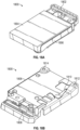
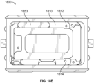
- FIGS. 18A, 18B , 18C, 18D , and 18E illustrate three grounding points 1810, 1814 and 1812 directly in contact with the metal housing.
- the wearable device can include a battery 1804 enclosed at least partially within a metal bracket 1806, the slot antenna 1853 including the tab configuration 1802, the slot antenna that can be excited by a monopole antenna 1808, and three grounding points 1810, 1814 and 1812.
- the first and second grounding points 1810 and 1814 can define the length of the slot antenna.
- the first and second grounding points 1810 and 1814 can be designed to be placed at certain locations to tune the slot length to resonate at the BLUETOOTH ® frequency band.
- the third grounding point 1812 can help improve the performance of the antenna by breaking the gap structure outside the radiation slot.
- the third grounding point 1812 can be designed to prevent unwanted resonances in the rest of the slot area, which could interfere with the slot's radiation efficiency.
- the PCB can be grounded to the metal housing at the three grounding points 1816, 1814 and 1812.
- the second and third grounding points 1814 and 1812, the PCB may not be directly connected to the metal housing but through a PCB bracket.
- Other grounding points can be implemented using other metal components to reduce coupling to the slot antenna.
- the antenna slot length can be changed by moving the first grounding point 1810.
- the location of the first grounding point 1810 can be moved closer to grounding point 1812 which will increase the length of the slot antenna because the length of the slot antenna is defined by the first and second grounding points 1810, 1814.
- the welding clip associated with the first grounding point 1810 can be removed to adjust the length of the slot antenna.
- the welding clip associated with the first grounding point 1810 can be removed 1882 as shown in FIG. 18C . Removing the welding clip associated with the first grounding point 1810 and using the screw grounding 1812 close to the clip at the other end of the slot could achieve additional length on the slot antenna.
- the end bracket can be moved to adjust the length of the slot antenna. For example, the end bracket can be extended closer to the top of the wearable device 1884 as shown in FIG. 18C . Because the length of the slot antenna can be the distance between the first grounding point 1810 and the second grounding point 1814, extending the end bracket towards the end of the device 1884 can achieve a longer length of the slot antenna. In some embodiments, the end bracket can be shortened (moved away from the end of the device 1884) to achieve a shorter length of the slot antenna.
- the device 1900 can include a touch module 1932 and/or a display module 1934.
- the touch module 1932 can be configured to detect touch input on the display window 1930.
- the display module 1934 can be configured to display images or information through the display window 1930.
- a dielectric gap e.g. air or plastic or combination of air and plastic
- the dielectric gap can create a back cavity for the slot antenna within an enclosed metal housing design.
- the dielectric gap can vary in height and/or can insure isolation between the PCB 1940 and to the metal bracket 1910.
- the dielectric gap also can insure isolation between the PCB 1940 and to the metal housing 1905.
- the battery 1950 can be located below the PCB 1940 and not need to be reduced in size.
- the efficiency of the slot antenna 1915 is generally higher when the direct feed 1947 is located closer to display window 1930.
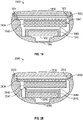
- FIG. 20 illustrate a cross-section along the width of another example wearable electronic device 2000 having a metal bracket 2010 within a metal housing 2005 forming a slot antenna 2015 that is excited by a direct feed 2047 from a printed circuit board 2040, where the direct feed 2047 is connected to the printed circuit board 2040 and the metal bracket 2010 and the dielectric gap 2046 is between the printed circuit board 2040 and the metal bracket 2010.
- the direct feed 2047 can be implemented using a spring clip or pogo pin to connect the feed 2047 from the PCB 2040 to the metal bracket 2010.
- the printed circuit board 2040 can be positioned within the metal housing 2005. For example, the printed circuit board 2040 can be positioned above the metal bracket 2010.
- the metal housing 2005 can include two or more grounding pins or grounding connections that electrically couple the metal housing 2005 at targeted locations to define the length of the slot antenna 2015 and/or to improve performance (e.g., by reducing unwanted resonances).
- the battery 2050 can be positioned below most of the metal bracket 2010.
- a dielectric gap e.g. air or plastic or combination of air and plastic
- the dielectric gap can create a back cavity for the slot antenna within an enclosed metal housing design.
- the dielectric gap can vary in height and/or can insure isolation between the PCB 2040 and to the metal bracket 2010.
- the dielectric gap also can insure isolation between the PCB 2040 and to the metal housing 2005.
- the battery 2050 can be located below the PCB 2040 and not need to be reduced in size.
- the efficiency of the slot antenna 2015 was found to be higher than in the implementation shown in FIG. 19 , possibly because there was lower current and lower loss in the connections between the metal bracket 2010 and the metal housing 2005.
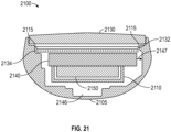
- the metal housing 2105 can include two or more grounding pins or grounding connections that electrically couple the metal housing 2105 at targeted locations to define the length of the slot antenna 2115 and/or to improve performance (e.g., by reducing unwanted resonances).
- the battery 2150 can be positioned above most of the metal bracket 2110.
- the device 2100 can include a touch module 2132 and/or a display module 2134.
- the touch module 2132 can be configured to detect touch input on the display window 2130.
- the display module 2134 can be configured to display images or information through the display window 2130.
- a dielectric gap e.g. air or plastic or combination of air and plastic
- the dielectric gap can create a back cavity for the slot antenna within an enclosed metal housing design.
- the dielectric gap can vary in height and/or can insure isolation between the metal bracket 2110 and to the metal housing 2105.
Landscapes
- Engineering & Computer Science (AREA)
- Computer Hardware Design (AREA)
- General Engineering & Computer Science (AREA)
- Power Engineering (AREA)
- Support Of Aerials (AREA)
- Details Of Aerials (AREA)
Claims (14)
- Computergerät (100), umfassend:ein leitfähiges Gehäuse (105) mit einer oder mehreren Innenflächen;eine Stromquelle (135);eine leitfähige Halterung (110), die eine oder mehrere Kanten oder Oberflächen aufweist, wobei die leitfähige Halterung in dem leitfähigen Gehäuse enthalten ist, die eine oder die mehreren Kanten oder Oberflächen der leitfähigen Halterung und die eine oder die mehreren Innenflächen des leitfähigen Gehäuses einen ersten Spalt dazwischen bilden, und ein Abschnitt des ersten Spalts eine Schlitzantenne (115) bildet;eine Monopolantenne (120);eine Antennenanpassungsschaltung;eine Leiterplatte (140) mit einer oder mehreren Kanten, wobei die eine oder die mehreren Kanten der Leiterplatte und die eine oder die mehreren Innenflächen des leitfähigen Gehäuses einen Spalt dazwischen bilden, wobei die Leiterplatte über die Antennenanpassungsschaltung mit der Monopolantenne gekoppelt ist und konfiguriert ist, die Monopolantenne anzusteuern, wobei die Monopolantenne so konfiguriert ist, dass sie elektromagnetische Felder erzeugt, um die Schlitzantenne zu veranlassen, Hochfrequenzsignale zu übertragen, wobei die Leiterplatte und die leitfähige Halterung ferner einen hinteren Hohlraum dazwischen bilden, wobei der hintere Hohlraum einen dielektrischen Spalt umfasst und eine Resonanz der Schlitzantenne begünstigt; undeine Anzeige (130, 134) innerhalb des leitfähigen Gehäuses, wobei sich eine Totzone der Anzeige mit einer Totzone aufgrund der Monopolantenne überschneidet;wobei sich die Stromquelle, die leitfähige Halterung, die Monopolantenne, die Antennenanpassungsschaltung und die Leiterplatte innerhalb von Wänden des leitfähigen Gehäuses befinden.
- Gerät nach Anspruch 1, wobei die Totzone der Anzeige und die Totzone aufgrund der Monopolantenne jeweils einen Raum zwischen einer Innenfläche des leitfähigen Gehäuses und einer Kante oder Oberfläche der leitfähigen Halterung beinhalten.
- Gerät nach Anspruch 1, wobei die Totzone aufgrund der Monopolantenne innerhalb der Totzone der Anzeige liegt.
- Gerät nach Anspruch 1, wobei die Totzone aufgrund der Monopolantenne innerhalb eines definierten Abstands einer Oberseite der Anzeige angeordnet ist.
- Gerät nach Anspruch 1, wobei die Schlitzantenne an mehr als zwei Kanten oder Oberflächen der leitfähigen Halterung ausgebildet ist.
- Gerät nach Anspruch 1, wobei die Schlitzantenne nicht direkt durch eine Antenneneinspeisung, die physisch mit der Leiterplatte gekoppelt ist, erregt wird.
- Gerät nach Anspruch 1, das ferner eine Nahfeldkommunikationsantenne (145) umfasst, wobei sich die Nahfeldkommunikationsantenne oberhalb der Stromquelle innerhalb des leitfähigen Gehäuses und unterhalb der Anzeige befindet.
- Gerät nach Anspruch 1, wobei die Stromquelle zumindest teilweise von der leitfähigen Halterung umgeben ist, sodass sich eine untere Oberfläche der Stromquelle angrenzend an eine obere Oberfläche der leitfähigen Halterung und innerhalb des leitfähigen Gehäuses befindet, wobei sich die Leiterplatte unterhalb der leitfähigen Halterung befindet.
- Gerät nach Anspruch 1, wobei die leitfähige Halterung einen ersten Erdungsanschluss an einem ersten Ende der Schlitzantenne und einen zweiten Erdungsanschluss an einem zweiten Ende der Schlitzantenne beinhaltet, wobei der erste Erdungsanschluss und der zweite Erdungsanschluss so konfiguriert sind, dass sie die leitfähige Halterung und das leitfähige Gehäuse elektrisch koppeln.
- Gerät nach Anspruch 9, wobei die leitfähige Halterung ferner einen dritten Erdungsstift über den ersten Spalt hinweg zwischen der leitfähigen Halterung und dem leitfähigen Gehäuse beinhaltet, wobei sich der dritte Erdungsstift nicht in einem Abschnitt des ersten Spalts, der die Schlitzantenne bildet, befindet.
- Gerät nach Anspruch 1, wobei die Schlitzantenne vollständig innerhalb des leitfähigen Gehäuses angeordnet ist, um eine Beeinträchtigung einer wasserdichten Dichtung, die zwischen der Anzeige und dem leitfähigen Gehäuse ausgebildet ist, zu verhindern.
- Gerät nach Anspruch 1, das ferner einen Berührungssensor zwischen einem Anzeigefenster und der Anzeige umfasst.
- Gerät nach Anspruch 1, wobei die Leiterplatte an mehreren Punkten um einen Umfang der Leiterplatte mit dem leitfähigen Gehäuse geerdet ist und sich nahe dem Boden des leitfähigen Gehäuses befindet.
- Gerät nach Anspruch 1, wobei die Stromquelle zumindest teilweise von der leitfähigen Halterung umgeben ist, sodass sich eine obere Oberfläche der Stromquelle angrenzend an eine untere Oberfläche der leitfähigen Halterung und innerhalb des leitfähigen Gehäuses befindet, wobei sich die Leiterplatte unterhalb der Stromquelle befindet.
Priority Applications (1)
| Application Number | Priority Date | Filing Date | Title |
|---|---|---|---|
| EP23153633.5A EP4191789A1 (de) | 2016-12-14 | 2017-12-14 | Verfahren für schlitzantennendesign für tragbare elektronische vorrichtungen und leitfähige gehäuse |
Applications Claiming Priority (2)
| Application Number | Priority Date | Filing Date | Title |
|---|---|---|---|
| US201662433994P | 2016-12-14 | 2016-12-14 | |
| PCT/US2017/066494 WO2018112246A1 (en) | 2016-12-14 | 2017-12-14 | Methods for slot antenna design for wearable electronic devices and conductive housings |
Related Child Applications (1)
| Application Number | Title | Priority Date | Filing Date |
|---|---|---|---|
| EP23153633.5A Division EP4191789A1 (de) | 2016-12-14 | 2017-12-14 | Verfahren für schlitzantennendesign für tragbare elektronische vorrichtungen und leitfähige gehäuse |
Publications (3)
| Publication Number | Publication Date |
|---|---|
| EP3555953A1 EP3555953A1 (de) | 2019-10-23 |
| EP3555953A4 EP3555953A4 (de) | 2020-08-12 |
| EP3555953B1 true EP3555953B1 (de) | 2023-02-01 |
Family
ID=62489745
Family Applications (2)
| Application Number | Title | Priority Date | Filing Date |
|---|---|---|---|
| EP17882182.3A Active EP3555953B1 (de) | 2016-12-14 | 2017-12-14 | Verfahren zum entwurf von schlitzantennen für elektronische wearable-vorrichtungen und leitfähige gehäuse |
| EP23153633.5A Pending EP4191789A1 (de) | 2016-12-14 | 2017-12-14 | Verfahren für schlitzantennendesign für tragbare elektronische vorrichtungen und leitfähige gehäuse |
Family Applications After (1)
| Application Number | Title | Priority Date | Filing Date |
|---|---|---|---|
| EP23153633.5A Pending EP4191789A1 (de) | 2016-12-14 | 2017-12-14 | Verfahren für schlitzantennendesign für tragbare elektronische vorrichtungen und leitfähige gehäuse |
Country Status (4)
| Country | Link |
|---|---|
| US (2) | US10320063B2 (de) |
| EP (2) | EP3555953B1 (de) |
| CN (1) | CN110168804B (de) |
| WO (1) | WO2018112246A1 (de) |
Families Citing this family (31)
| Publication number | Priority date | Publication date | Assignee | Title |
|---|---|---|---|---|
| CA2967409C (en) | 2014-11-10 | 2023-08-29 | In-Situ, Inc. | Integrated user interface for status and control of a submersible multi-parameter sonde |
| US10136543B1 (en) | 2016-12-14 | 2018-11-20 | Fitbit, Inc. | Inductance-based user interface elements |
| US10461402B2 (en) * | 2017-02-08 | 2019-10-29 | Intel Corporation | Mobile device with antenna-boosting case coupling |
| US10673127B2 (en) | 2018-05-29 | 2020-06-02 | Apple Inc. | Electronic device wide band antennas |
| US10734708B2 (en) * | 2018-07-11 | 2020-08-04 | Apple Inc. | Antennas formed from conductive display layers |
| CN109216942B (zh) * | 2018-09-11 | 2023-12-19 | 深圳市信维通信股份有限公司 | 基于金属框的5g毫米波移动终端天线系统 |
| US11394129B2 (en) | 2018-12-13 | 2022-07-19 | Fitbit, Inc. | Multiple band antenna structures |
| US10992029B2 (en) * | 2018-12-13 | 2021-04-27 | Fitbit, Inc. | Multiple band antenna structures |
| JP7123784B2 (ja) * | 2018-12-25 | 2022-08-23 | スタンレー電気株式会社 | タッチパネル付き表示装置 |
| JP7217207B2 (ja) * | 2019-07-10 | 2023-02-02 | 株式会社日立製作所 | アンテナ装置およびマンホール蓋の製造方法 |
| CN110459872B (zh) * | 2019-08-19 | 2021-07-16 | Oppo广东移动通信有限公司 | 壳体组件及电子设备 |
| CN110492233B (zh) * | 2019-08-19 | 2021-07-20 | Oppo(重庆)智能科技有限公司 | 壳体组件及电子设备 |
| CN110518332A (zh) * | 2019-08-28 | 2019-11-29 | 信维创科通信技术(北京)有限公司 | 一种基于金属边框缝隙的5gmimo天线系统 |
| US11262966B2 (en) | 2019-09-27 | 2022-03-01 | Apple Inc. | Electromagnetic band gap structures |
| KR102937103B1 (ko) * | 2019-12-31 | 2026-03-09 | 엘지디스플레이 주식회사 | 표시장치 |
| CN113161721B (zh) * | 2020-01-22 | 2023-11-28 | 华为技术有限公司 | 天线装置及电子设备 |
| CN113867122B (zh) * | 2020-06-30 | 2022-12-13 | 华为技术有限公司 | 可穿戴设备 |
| CN114079141B (zh) * | 2020-08-18 | 2025-01-24 | 青岛海信移动通信技术有限公司 | 电子设备 |
| CN111883717B (zh) * | 2020-08-31 | 2025-02-18 | 广东小天才科技有限公司 | 应用于可穿戴设备的电源装置和便携设备 |
| CN112952353B (zh) * | 2021-01-29 | 2024-09-06 | 捷开通讯(深圳)有限公司 | 一种天线结构以及智能设备 |
| CN112928437B (zh) * | 2021-02-05 | 2024-10-01 | 东莞市通锦新材料科技有限公司 | 一种可焊接的多功能天线及蓝牙穿戴设备 |
| KR20220124542A (ko) * | 2021-03-03 | 2022-09-14 | 삼성전자주식회사 | 그립 센싱 패드를 포함하는 전자 장치 |
| US11962069B2 (en) | 2021-03-03 | 2024-04-16 | Samsung Electronics Co., Ltd. | Electronic device including grip sensing pad |
| EP4305705B1 (de) * | 2021-03-12 | 2025-01-15 | Google LLC | Schirm für anzeigevorrichtung mit integrierter antenne |
| GB2605631B (en) * | 2021-04-07 | 2023-11-29 | Continental Automotive Tech Gmbh | Antenna structure for RF devices |
| EP4182772A1 (de) * | 2021-10-07 | 2023-05-24 | Fitbit LLC | Tragbare rechnervorrichtung mit einer oder mehreren biometrischen sensorelektroden auf einer abdeckung für einen anzeigebildschirm |
| US11962074B2 (en) * | 2022-03-04 | 2024-04-16 | Meta Platforms Technologies, Llc | Multi-band antenna architectures for a wearable device and related devices and methods |
| DE102022202761A1 (de) * | 2022-03-21 | 2023-09-21 | Sivantos Pte. Ltd. | Hörgerät |
| US12107328B2 (en) | 2022-05-31 | 2024-10-01 | Apple Inc. | Electronic devices with interconnected ground structures |
| CN115479076B (zh) * | 2022-08-31 | 2025-07-22 | 联想(北京)有限公司 | 转轴结构及电子设备 |
| WO2025216453A1 (ko) * | 2024-04-08 | 2025-10-16 | 삼성전자 주식회사 | 안테나를 포함하는 웨어러블 전자 장치 |
Family Cites Families (28)
| Publication number | Priority date | Publication date | Assignee | Title |
|---|---|---|---|---|
| US4091318A (en) * | 1977-02-16 | 1978-05-23 | Motorola Inc. | Charger/converter console with reel arrangement |
| CN101401258B (zh) | 2006-05-25 | 2012-10-10 | 松下电器产业株式会社 | 可变缝隙天线和其驱动方法 |
| US7876274B2 (en) * | 2007-06-21 | 2011-01-25 | Apple Inc. | Wireless handheld electronic device |
| US8106836B2 (en) * | 2008-04-11 | 2012-01-31 | Apple Inc. | Hybrid antennas for electronic devices |
| US8466839B2 (en) | 2009-07-17 | 2013-06-18 | Apple Inc. | Electronic devices with parasitic antenna resonating elements that reduce near field radiation |
| US8270914B2 (en) * | 2009-12-03 | 2012-09-18 | Apple Inc. | Bezel gap antennas |
| US8599089B2 (en) * | 2010-03-30 | 2013-12-03 | Apple Inc. | Cavity-backed slot antenna with near-field-coupled parasitic slot |
| US20120169547A1 (en) | 2011-01-03 | 2012-07-05 | Palm, Inc. | Multiband antenna with surrounding conductive cosmetic feature |
| US8693204B2 (en) * | 2011-01-10 | 2014-04-08 | Apple Inc. | Electronic devices having multi-purpose cowling structures and a compass mounted on a flex circuit |
| US8860619B2 (en) * | 2011-09-20 | 2014-10-14 | Netgear, Inc. | Wireless device and multi-antenna system having dual open-slot radiators |
| US9318793B2 (en) * | 2012-05-02 | 2016-04-19 | Apple Inc. | Corner bracket slot antennas |
| US9093745B2 (en) * | 2012-05-10 | 2015-07-28 | Apple Inc. | Antenna and proximity sensor structures having printed circuit and dielectric carrier layers |
| US9105899B2 (en) * | 2012-09-07 | 2015-08-11 | Apple Inc. | Electronic device subassemblies |
| US9520638B2 (en) | 2013-01-15 | 2016-12-13 | Fitbit, Inc. | Hybrid radio frequency / inductive loop antenna |
| US9865915B2 (en) * | 2013-02-28 | 2018-01-09 | Apple Inc. | Electronic device with diverse antenna array having soldered connections |
| US9215752B2 (en) | 2013-03-11 | 2015-12-15 | Google Technology Holdings LLC | Electronic device with through-display near field communication capability |
| US9153874B2 (en) * | 2013-03-18 | 2015-10-06 | Apple Inc. | Electronic device having multiport antenna structures with resonating slot |
| US9379427B2 (en) * | 2013-04-26 | 2016-06-28 | Apple Inc. | Methods for manufacturing an antenna tuning element in an electronic device |
| CN104466392B (zh) * | 2013-09-18 | 2018-01-23 | 联想(北京)有限公司 | 天线装置、电子设备和用于设置天线装置的方法 |
| US9196964B2 (en) | 2014-03-05 | 2015-11-24 | Fitbit, Inc. | Hybrid piezoelectric device / radio frequency antenna |
| US9559425B2 (en) * | 2014-03-20 | 2017-01-31 | Apple Inc. | Electronic device with slot antenna and proximity sensor |
| US9680205B2 (en) * | 2014-08-25 | 2017-06-13 | Apple Inc. | Electronic device with peripheral display antenna |
| CN104362427B (zh) * | 2014-11-14 | 2017-07-18 | 深圳市信维通信股份有限公司 | 基于金属框架的lte频段手机天线 |
| CN104538741B (zh) * | 2014-12-17 | 2017-12-26 | 小米科技有限责任公司 | 缝隙天线及具有导电边框的电子设备 |
| US10224602B2 (en) * | 2015-04-22 | 2019-03-05 | Apple Inc. | Electronic device with housing slots for antennas |
| CN204668449U (zh) * | 2015-04-24 | 2015-09-23 | 广州三星通信技术研究有限公司 | 用于电子设备的天线及电子设备 |
| US9876273B2 (en) * | 2015-09-03 | 2018-01-23 | Apple Inc. | Electronic device having antenna on grounded speaker box |
| CN105742794A (zh) * | 2016-02-03 | 2016-07-06 | 珠海市魅族科技有限公司 | 一种天线结构及终端 |
-
2017
- 2017-12-14 US US15/842,689 patent/US10320063B2/en active Active
- 2017-12-14 EP EP17882182.3A patent/EP3555953B1/de active Active
- 2017-12-14 CN CN201780082158.XA patent/CN110168804B/zh active Active
- 2017-12-14 EP EP23153633.5A patent/EP4191789A1/de active Pending
- 2017-12-14 WO PCT/US2017/066494 patent/WO2018112246A1/en not_active Ceased
-
2019
- 2019-01-22 US US16/254,395 patent/US10637129B2/en active Active
Also Published As
| Publication number | Publication date |
|---|---|
| US20190260116A1 (en) | 2019-08-22 |
| CN110168804B (zh) | 2021-12-28 |
| WO2018112246A1 (en) | 2018-06-21 |
| EP4191789A1 (de) | 2023-06-07 |
| CN110168804A (zh) | 2019-08-23 |
| EP3555953A1 (de) | 2019-10-23 |
| EP3555953A4 (de) | 2020-08-12 |
| US10637129B2 (en) | 2020-04-28 |
| US20180166772A1 (en) | 2018-06-14 |
| US10320063B2 (en) | 2019-06-11 |
Similar Documents
| Publication | Publication Date | Title |
|---|---|---|
| EP3555953B1 (de) | Verfahren zum entwurf von schlitzantennen für elektronische wearable-vorrichtungen und leitfähige gehäuse | |
| US10892565B2 (en) | Multiple band antenna structures | |
| US11482773B2 (en) | Multiple band antenna structures | |
| EP3317919B1 (de) | Antennen mit gekoppelten multibändern in drahtlosen wearable-vorrichtungen | |
| US9509054B2 (en) | Compact polarized antenna and methods | |
| CN111755805B (zh) | 天线模组和电子设备 | |
| KR101658766B1 (ko) | 다목적 안테나 | |
| US9647338B2 (en) | Coupled antenna structure and methods | |
| US10079428B2 (en) | Coupled antenna structure and methods | |
| US11853016B2 (en) | Electronic device wide band antennas | |
| US8963794B2 (en) | Distributed loop antennas | |
| US20200259258A1 (en) | Electronic Device Having Multi-Frequency Ultra-Wideband Antennas | |
| US20210098869A1 (en) | Electronic Device Wide Band Antennas | |
| CN115411498B (zh) | 穿戴设备 | |
| KR102951814B1 (ko) | 안테나를 포함하는 전자 장치 | |
| US20150077293A1 (en) | Short-range antenna structure and methods | |
| CN112886206B (zh) | 穿戴式电子设备 | |
| CN112886207B (zh) | 穿戴式电子设备 | |
| CN112886212B (zh) | 穿戴式电子设备 | |
| CN115528418B (zh) | 天线单元和电子设备 | |
| CN120143590A (zh) | 手表 | |
| CN117096595A (zh) | 一种电子设备 |
Legal Events
| Date | Code | Title | Description |
|---|---|---|---|
| STAA | Information on the status of an ep patent application or granted ep patent |
Free format text: STATUS: THE INTERNATIONAL PUBLICATION HAS BEEN MADE |
|
| PUAI | Public reference made under article 153(3) epc to a published international application that has entered the european phase |
Free format text: ORIGINAL CODE: 0009012 |
|
| STAA | Information on the status of an ep patent application or granted ep patent |
Free format text: STATUS: REQUEST FOR EXAMINATION WAS MADE |
|
| 17P | Request for examination filed |
Effective date: 20190605 |
|
| AK | Designated contracting states |
Kind code of ref document: A1 Designated state(s): AL AT BE BG CH CY CZ DE DK EE ES FI FR GB GR HR HU IE IS IT LI LT LU LV MC MK MT NL NO PL PT RO RS SE SI SK SM TR |
|
| AX | Request for extension of the european patent |
Extension state: BA ME |
|
| DAV | Request for validation of the european patent (deleted) | ||
| DAX | Request for extension of the european patent (deleted) | ||
| A4 | Supplementary search report drawn up and despatched |
Effective date: 20200713 |
|
| RIC1 | Information provided on ipc code assigned before grant |
Ipc: H01Q 1/44 20060101ALI20200707BHEP Ipc: H01Q 1/24 20060101ALN20200707BHEP Ipc: H01Q 13/18 20060101ALI20200707BHEP Ipc: H01Q 1/27 20060101AFI20200707BHEP |
|
| GRAP | Despatch of communication of intention to grant a patent |
Free format text: ORIGINAL CODE: EPIDOSNIGR1 |
|
| STAA | Information on the status of an ep patent application or granted ep patent |
Free format text: STATUS: GRANT OF PATENT IS INTENDED |
|
| RIC1 | Information provided on ipc code assigned before grant |
Ipc: H01Q 1/24 20060101ALN20211122BHEP Ipc: H01Q 1/44 20060101ALI20211122BHEP Ipc: H01Q 13/18 20060101ALI20211122BHEP Ipc: H01Q 1/27 20060101AFI20211122BHEP |
|
| RIC1 | Information provided on ipc code assigned before grant |
Ipc: H01Q 1/24 20060101ALN20211130BHEP Ipc: H01Q 1/44 20060101ALI20211130BHEP Ipc: H01Q 13/18 20060101ALI20211130BHEP Ipc: H01Q 1/27 20060101AFI20211130BHEP |
|
| INTG | Intention to grant announced |
Effective date: 20211217 |
|
| RIC1 | Information provided on ipc code assigned before grant |
Ipc: H01Q 1/24 20060101ALN20211207BHEP Ipc: H01Q 1/44 20060101ALI20211207BHEP Ipc: H01Q 13/18 20060101ALI20211207BHEP Ipc: H01Q 1/27 20060101AFI20211207BHEP |
|
| GRAJ | Information related to disapproval of communication of intention to grant by the applicant or resumption of examination proceedings by the epo deleted |
Free format text: ORIGINAL CODE: EPIDOSDIGR1 |
|
| STAA | Information on the status of an ep patent application or granted ep patent |
Free format text: STATUS: REQUEST FOR EXAMINATION WAS MADE |
|
| INTC | Intention to grant announced (deleted) | ||
| RIC1 | Information provided on ipc code assigned before grant |
Ipc: H01Q 1/24 20060101ALN20220519BHEP Ipc: H01Q 1/44 20060101ALI20220519BHEP Ipc: H01Q 13/18 20060101ALI20220519BHEP Ipc: H01Q 1/27 20060101AFI20220519BHEP |
|
| REG | Reference to a national code |
Ref country code: DE Ref legal event code: R079 Ref document number: 602017065917 Country of ref document: DE Free format text: PREVIOUS MAIN CLASS: H01Q0001220000 Ipc: H01Q0001270000 |
|
| GRAP | Despatch of communication of intention to grant a patent |
Free format text: ORIGINAL CODE: EPIDOSNIGR1 |
|
| STAA | Information on the status of an ep patent application or granted ep patent |
Free format text: STATUS: GRANT OF PATENT IS INTENDED |
|
| RIC1 | Information provided on ipc code assigned before grant |
Ipc: H01Q 1/24 20060101ALN20220712BHEP Ipc: H01Q 1/44 20060101ALI20220712BHEP Ipc: H01Q 13/18 20060101ALI20220712BHEP Ipc: H01Q 1/27 20060101AFI20220712BHEP |
|
| INTG | Intention to grant announced |
Effective date: 20220809 |
|
| GRAS | Grant fee paid |
Free format text: ORIGINAL CODE: EPIDOSNIGR3 |
|
| GRAA | (expected) grant |
Free format text: ORIGINAL CODE: 0009210 |
|
| STAA | Information on the status of an ep patent application or granted ep patent |
Free format text: STATUS: THE PATENT HAS BEEN GRANTED |
|
| AK | Designated contracting states |
Kind code of ref document: B1 Designated state(s): AL AT BE BG CH CY CZ DE DK EE ES FI FR GB GR HR HU IE IS IT LI LT LU LV MC MK MT NL NO PL PT RO RS SE SI SK SM TR |
|
| REG | Reference to a national code |
Ref country code: GB Ref legal event code: FG4D |
|
| REG | Reference to a national code |
Ref country code: CH Ref legal event code: EP Ref country code: AT Ref legal event code: REF Ref document number: 1547161 Country of ref document: AT Kind code of ref document: T Effective date: 20230215 |
|
| REG | Reference to a national code |
Ref country code: DE Ref legal event code: R096 Ref document number: 602017065917 Country of ref document: DE |
|
| REG | Reference to a national code |
Ref country code: IE Ref legal event code: FG4D |
|
| REG | Reference to a national code |
Ref country code: LT Ref legal event code: MG9D |
|
| REG | Reference to a national code |
Ref country code: NL Ref legal event code: MP Effective date: 20230201 |
|
| P01 | Opt-out of the competence of the unified patent court (upc) registered |
Effective date: 20230516 |
|
| REG | Reference to a national code |
Ref country code: AT Ref legal event code: MK05 Ref document number: 1547161 Country of ref document: AT Kind code of ref document: T Effective date: 20230201 |
|
| PG25 | Lapsed in a contracting state [announced via postgrant information from national office to epo] |
Ref country code: RS Free format text: LAPSE BECAUSE OF FAILURE TO SUBMIT A TRANSLATION OF THE DESCRIPTION OR TO PAY THE FEE WITHIN THE PRESCRIBED TIME-LIMIT Effective date: 20230201 Ref country code: PT Free format text: LAPSE BECAUSE OF FAILURE TO SUBMIT A TRANSLATION OF THE DESCRIPTION OR TO PAY THE FEE WITHIN THE PRESCRIBED TIME-LIMIT Effective date: 20230601 Ref country code: NO Free format text: LAPSE BECAUSE OF FAILURE TO SUBMIT A TRANSLATION OF THE DESCRIPTION OR TO PAY THE FEE WITHIN THE PRESCRIBED TIME-LIMIT Effective date: 20230501 Ref country code: NL Free format text: LAPSE BECAUSE OF FAILURE TO SUBMIT A TRANSLATION OF THE DESCRIPTION OR TO PAY THE FEE WITHIN THE PRESCRIBED TIME-LIMIT Effective date: 20230201 Ref country code: LV Free format text: LAPSE BECAUSE OF FAILURE TO SUBMIT A TRANSLATION OF THE DESCRIPTION OR TO PAY THE FEE WITHIN THE PRESCRIBED TIME-LIMIT Effective date: 20230201 Ref country code: LT Free format text: LAPSE BECAUSE OF FAILURE TO SUBMIT A TRANSLATION OF THE DESCRIPTION OR TO PAY THE FEE WITHIN THE PRESCRIBED TIME-LIMIT Effective date: 20230201 Ref country code: HR Free format text: LAPSE BECAUSE OF FAILURE TO SUBMIT A TRANSLATION OF THE DESCRIPTION OR TO PAY THE FEE WITHIN THE PRESCRIBED TIME-LIMIT Effective date: 20230201 Ref country code: ES Free format text: LAPSE BECAUSE OF FAILURE TO SUBMIT A TRANSLATION OF THE DESCRIPTION OR TO PAY THE FEE WITHIN THE PRESCRIBED TIME-LIMIT Effective date: 20230201 Ref country code: AT Free format text: LAPSE BECAUSE OF FAILURE TO SUBMIT A TRANSLATION OF THE DESCRIPTION OR TO PAY THE FEE WITHIN THE PRESCRIBED TIME-LIMIT Effective date: 20230201 |
|
| PG25 | Lapsed in a contracting state [announced via postgrant information from national office to epo] |
Ref country code: SE Free format text: LAPSE BECAUSE OF FAILURE TO SUBMIT A TRANSLATION OF THE DESCRIPTION OR TO PAY THE FEE WITHIN THE PRESCRIBED TIME-LIMIT Effective date: 20230201 Ref country code: PL Free format text: LAPSE BECAUSE OF FAILURE TO SUBMIT A TRANSLATION OF THE DESCRIPTION OR TO PAY THE FEE WITHIN THE PRESCRIBED TIME-LIMIT Effective date: 20230201 Ref country code: IS Free format text: LAPSE BECAUSE OF FAILURE TO SUBMIT A TRANSLATION OF THE DESCRIPTION OR TO PAY THE FEE WITHIN THE PRESCRIBED TIME-LIMIT Effective date: 20230601 Ref country code: GR Free format text: LAPSE BECAUSE OF FAILURE TO SUBMIT A TRANSLATION OF THE DESCRIPTION OR TO PAY THE FEE WITHIN THE PRESCRIBED TIME-LIMIT Effective date: 20230502 Ref country code: FI Free format text: LAPSE BECAUSE OF FAILURE TO SUBMIT A TRANSLATION OF THE DESCRIPTION OR TO PAY THE FEE WITHIN THE PRESCRIBED TIME-LIMIT Effective date: 20230201 |
|
| PG25 | Lapsed in a contracting state [announced via postgrant information from national office to epo] |
Ref country code: SM Free format text: LAPSE BECAUSE OF FAILURE TO SUBMIT A TRANSLATION OF THE DESCRIPTION OR TO PAY THE FEE WITHIN THE PRESCRIBED TIME-LIMIT Effective date: 20230201 Ref country code: RO Free format text: LAPSE BECAUSE OF FAILURE TO SUBMIT A TRANSLATION OF THE DESCRIPTION OR TO PAY THE FEE WITHIN THE PRESCRIBED TIME-LIMIT Effective date: 20230201 Ref country code: EE Free format text: LAPSE BECAUSE OF FAILURE TO SUBMIT A TRANSLATION OF THE DESCRIPTION OR TO PAY THE FEE WITHIN THE PRESCRIBED TIME-LIMIT Effective date: 20230201 Ref country code: DK Free format text: LAPSE BECAUSE OF FAILURE TO SUBMIT A TRANSLATION OF THE DESCRIPTION OR TO PAY THE FEE WITHIN THE PRESCRIBED TIME-LIMIT Effective date: 20230201 Ref country code: CZ Free format text: LAPSE BECAUSE OF FAILURE TO SUBMIT A TRANSLATION OF THE DESCRIPTION OR TO PAY THE FEE WITHIN THE PRESCRIBED TIME-LIMIT Effective date: 20230201 |
|
| REG | Reference to a national code |
Ref country code: DE Ref legal event code: R097 Ref document number: 602017065917 Country of ref document: DE |
|
| PG25 | Lapsed in a contracting state [announced via postgrant information from national office to epo] |
Ref country code: SK Free format text: LAPSE BECAUSE OF FAILURE TO SUBMIT A TRANSLATION OF THE DESCRIPTION OR TO PAY THE FEE WITHIN THE PRESCRIBED TIME-LIMIT Effective date: 20230201 |
|
| PLBE | No opposition filed within time limit |
Free format text: ORIGINAL CODE: 0009261 |
|
| STAA | Information on the status of an ep patent application or granted ep patent |
Free format text: STATUS: NO OPPOSITION FILED WITHIN TIME LIMIT |
|
| 26N | No opposition filed |
Effective date: 20231103 |
|
| PG25 | Lapsed in a contracting state [announced via postgrant information from national office to epo] |
Ref country code: SI Free format text: LAPSE BECAUSE OF FAILURE TO SUBMIT A TRANSLATION OF THE DESCRIPTION OR TO PAY THE FEE WITHIN THE PRESCRIBED TIME-LIMIT Effective date: 20230201 |
|
| PG25 | Lapsed in a contracting state [announced via postgrant information from national office to epo] |
Ref country code: IT Free format text: LAPSE BECAUSE OF FAILURE TO SUBMIT A TRANSLATION OF THE DESCRIPTION OR TO PAY THE FEE WITHIN THE PRESCRIBED TIME-LIMIT Effective date: 20230201 |
|
| REG | Reference to a national code |
Ref country code: CH Ref legal event code: PL |
|
| PG25 | Lapsed in a contracting state [announced via postgrant information from national office to epo] |
Ref country code: LU Free format text: LAPSE BECAUSE OF NON-PAYMENT OF DUE FEES Effective date: 20231214 |
|
| PG25 | Lapsed in a contracting state [announced via postgrant information from national office to epo] |
Ref country code: MC Free format text: LAPSE BECAUSE OF FAILURE TO SUBMIT A TRANSLATION OF THE DESCRIPTION OR TO PAY THE FEE WITHIN THE PRESCRIBED TIME-LIMIT Effective date: 20230201 |
|
| GBPC | Gb: european patent ceased through non-payment of renewal fee |
Effective date: 20231214 |
|
| REG | Reference to a national code |
Ref country code: BE Ref legal event code: MM Effective date: 20231231 |
|
| PG25 | Lapsed in a contracting state [announced via postgrant information from national office to epo] |
Ref country code: MC Free format text: LAPSE BECAUSE OF FAILURE TO SUBMIT A TRANSLATION OF THE DESCRIPTION OR TO PAY THE FEE WITHIN THE PRESCRIBED TIME-LIMIT Effective date: 20230201 Ref country code: LU Free format text: LAPSE BECAUSE OF NON-PAYMENT OF DUE FEES Effective date: 20231214 |
|
| REG | Reference to a national code |
Ref country code: IE Ref legal event code: MM4A |
|
| PG25 | Lapsed in a contracting state [announced via postgrant information from national office to epo] |
Ref country code: IE Free format text: LAPSE BECAUSE OF NON-PAYMENT OF DUE FEES Effective date: 20231214 |
|
| PG25 | Lapsed in a contracting state [announced via postgrant information from national office to epo] |
Ref country code: GB Free format text: LAPSE BECAUSE OF NON-PAYMENT OF DUE FEES Effective date: 20231214 |
|
| PG25 | Lapsed in a contracting state [announced via postgrant information from national office to epo] |
Ref country code: BE Free format text: LAPSE BECAUSE OF NON-PAYMENT OF DUE FEES Effective date: 20231231 |
|
| PG25 | Lapsed in a contracting state [announced via postgrant information from national office to epo] |
Ref country code: FR Free format text: LAPSE BECAUSE OF NON-PAYMENT OF DUE FEES Effective date: 20231231 |
|
| PG25 | Lapsed in a contracting state [announced via postgrant information from national office to epo] |
Ref country code: CH Free format text: LAPSE BECAUSE OF NON-PAYMENT OF DUE FEES Effective date: 20231231 |
|
| PG25 | Lapsed in a contracting state [announced via postgrant information from national office to epo] |
Ref country code: IE Free format text: LAPSE BECAUSE OF NON-PAYMENT OF DUE FEES Effective date: 20231214 Ref country code: GB Free format text: LAPSE BECAUSE OF NON-PAYMENT OF DUE FEES Effective date: 20231214 Ref country code: FR Free format text: LAPSE BECAUSE OF NON-PAYMENT OF DUE FEES Effective date: 20231231 Ref country code: CH Free format text: LAPSE BECAUSE OF NON-PAYMENT OF DUE FEES Effective date: 20231231 Ref country code: BE Free format text: LAPSE BECAUSE OF NON-PAYMENT OF DUE FEES Effective date: 20231231 |
|
| PG25 | Lapsed in a contracting state [announced via postgrant information from national office to epo] |
Ref country code: BG Free format text: LAPSE BECAUSE OF FAILURE TO SUBMIT A TRANSLATION OF THE DESCRIPTION OR TO PAY THE FEE WITHIN THE PRESCRIBED TIME-LIMIT Effective date: 20230201 |
|
| PG25 | Lapsed in a contracting state [announced via postgrant information from national office to epo] |
Ref country code: BG Free format text: LAPSE BECAUSE OF FAILURE TO SUBMIT A TRANSLATION OF THE DESCRIPTION OR TO PAY THE FEE WITHIN THE PRESCRIBED TIME-LIMIT Effective date: 20230201 |
|
| PG25 | Lapsed in a contracting state [announced via postgrant information from national office to epo] |
Ref country code: CY Free format text: LAPSE BECAUSE OF FAILURE TO SUBMIT A TRANSLATION OF THE DESCRIPTION OR TO PAY THE FEE WITHIN THE PRESCRIBED TIME-LIMIT; INVALID AB INITIO Effective date: 20171214 |
|
| PG25 | Lapsed in a contracting state [announced via postgrant information from national office to epo] |
Ref country code: HU Free format text: LAPSE BECAUSE OF FAILURE TO SUBMIT A TRANSLATION OF THE DESCRIPTION OR TO PAY THE FEE WITHIN THE PRESCRIBED TIME-LIMIT; INVALID AB INITIO Effective date: 20171214 |
|
| PG25 | Lapsed in a contracting state [announced via postgrant information from national office to epo] |
Ref country code: TR Free format text: LAPSE BECAUSE OF FAILURE TO SUBMIT A TRANSLATION OF THE DESCRIPTION OR TO PAY THE FEE WITHIN THE PRESCRIBED TIME-LIMIT Effective date: 20230201 |
|
| PGFP | Annual fee paid to national office [announced via postgrant information from national office to epo] |
Ref country code: DE Payment date: 20251229 Year of fee payment: 9 |