EP3555962B1 - Radiateur polyvalent à polarisation - Google Patents
Radiateur polyvalent à polarisation Download PDFInfo
- Publication number
- EP3555962B1 EP3555962B1 EP17826059.2A EP17826059A EP3555962B1 EP 3555962 B1 EP3555962 B1 EP 3555962B1 EP 17826059 A EP17826059 A EP 17826059A EP 3555962 B1 EP3555962 B1 EP 3555962B1
- Authority
- EP
- European Patent Office
- Prior art keywords
- layer
- pair
- feed
- dilation
- disposed
- Prior art date
- Legal status (The legal status is an assumption and is not a legal conclusion. Google has not performed a legal analysis and makes no representation as to the accuracy of the status listed.)
- Active
Links
Images


Classifications
-
- H—ELECTRICITY
- H01—ELECTRIC ELEMENTS
- H01Q—ANTENNAS, i.e. RADIO AERIALS
- H01Q21/00—Antenna arrays or systems
- H01Q21/0006—Particular feeding systems
-
- H—ELECTRICITY
- H01—ELECTRIC ELEMENTS
- H01Q—ANTENNAS, i.e. RADIO AERIALS
- H01Q21/00—Antenna arrays or systems
-
- H—ELECTRICITY
- H01—ELECTRIC ELEMENTS
- H01Q—ANTENNAS, i.e. RADIO AERIALS
- H01Q21/00—Antenna arrays or systems
- H01Q21/06—Arrays of individually energised antenna units similarly polarised and spaced apart
-
- H—ELECTRICITY
- H01—ELECTRIC ELEMENTS
- H01Q—ANTENNAS, i.e. RADIO AERIALS
- H01Q21/00—Antenna arrays or systems
- H01Q21/06—Arrays of individually energised antenna units similarly polarised and spaced apart
- H01Q21/061—Two dimensional planar arrays
-
- H—ELECTRICITY
- H01—ELECTRIC ELEMENTS
- H01Q—ANTENNAS, i.e. RADIO AERIALS
- H01Q21/00—Antenna arrays or systems
- H01Q21/24—Combinations of antenna units polarised in different directions for transmitting or receiving circularly and elliptically polarised waves or waves linearly polarised in any direction
-
- H—ELECTRICITY
- H01—ELECTRIC ELEMENTS
- H01Q—ANTENNAS, i.e. RADIO AERIALS
- H01Q9/00—Electrically-short antennas having dimensions not more than twice the operating wavelength and consisting of conductive active radiating elements
- H01Q9/04—Resonant antennas
-
- H—ELECTRICITY
- H01—ELECTRIC ELEMENTS
- H01Q—ANTENNAS, i.e. RADIO AERIALS
- H01Q9/00—Electrically-short antennas having dimensions not more than twice the operating wavelength and consisting of conductive active radiating elements
- H01Q9/04—Resonant antennas
- H01Q9/0407—Substantially flat resonant element parallel to ground plane, e.g. patch antenna
- H01Q9/0414—Substantially flat resonant element parallel to ground plane, e.g. patch antenna in a stacked or folded configuration
Definitions
- RF systems e.g. radar or communication systems
- some RF systems include antennas having radiator elements which are responsive to RF signals having two orthogonal polarizations (so-called dual-polarized radiators).
- AESA antennas find use in a wide range of military and non-military applications including water based (e.g. naval), air-based and land-based applications.
- a cross-polarization isolation characteristic of an RF system refers to the ability of the system to simultaneously receive an RF signal having a first polarization on a first signal channel while isolating an RF signal having a second, orthogonal polarization from the signal channel. The greater the cross-polarization isolation characteristic, the greater the effectiveness with which the RF system can operate.
- a cavity backed aperture coupled dielectrically loaded waveguide radiating element with even mode excitation and wide angle impedance matching is known from US9225070B1 .
- a unit cell of an array antenna comprises an integrated dilation and feed circuit and an associated radiator assembly.
- the integrated dilation and feed circuit includes a dilation layer having first and second transmission lines. One end of each dilation layer transmission lines is configured to be coupled to a transceiver and the other end of each dilation layer transmission line is coupled to an antenna element of a radiator assembly through combiner, feed and slot layers of the integrated dilation and feed circuit.
- the combiner layer includes a pair of reactive combiner circuits.
- the combiner circuit has asymmetric physical features -and a plurality of via holes are provided in the combiner layer between signal paths of the combiner circuit.
- a first port of each reactive combiner circuit is coupled to a respective one of the dilation circuits.
- Second and third ports of each reactive combiner circuit are coupled to a first port of respective ones of four feed circuits symmetrically disposed on a feed layer.
- the feed circuits are configured to couple RF signals to/from a pair of orthogonally disposed slot aperture coupling elements (e.g. slot aperture couplers) symmetrically disposed on the slot layer of the integrated dilation-feed circuit.
- the slot layer couples signals to and from the radiator assembly.
- an integrated dilation-feed circuit having physical symmetry in feed and slot layers and which may be used in a unit cell of a polarization diverse antenna element is provided.
- the radiator assembly includes a symmetric dual-polarized antenna element.
- a symmetric dual-polarized antenna element may be coupled to the symmetric, integrated dilation-feed circuit.
- the physical symmetry of the integrated dilation-feed circuit and the dual-polarized antenna element results in a dual-polarized antenna element unit cell having both physical and electromagnetic field symmetry.
- the integrated dilation-feed circuit and antenna element are responsive to RF signals having any polarization (i.e. a polarization diverse antenna element and integrated dilation and feed circuit is provided) by nature of the vector combination of the two described orthogonal polarizations.
- the integrated dilation-feed circuit and associated radiator assembly together form a polarization diverse antenna unit cell and a plurality of such polarization diverse unit cells may be disposed to provide a polarization diverse array antenna.
- the symmetry in both the integrated dilation-feed circuit and antenna element allows a high degree of polarization isolation to be achieved in a polarization diverse array antenna.
- Such a polarization diverse array antenna may be provided as part of a radar system.
- the polarization diverse array antenna may be provided as a polarization diverse AESA antenna.
- the symmetric integrated dilation-feed circuit aligns an antenna element lattice structure (and thus the unit cell lattice) with a lattice structure of a transmit/receive integrated microwave module (TRIMM).
- TRIMM transmit/receive integrated microwave module
- a polarization diverse radar system comprises a polarization diverse AESA antenna provided from a plurality of unit cells with each of the unit cells comprising a polarization diverse antenna element.
- the radar system is responsive to RF signals having orthogonal circular polarizations as well as signals having orthogonal linear polarizations.
- the polarization diverse antenna is simultaneously responsive to RF signals having orthogonal circular and orthogonal linear polarizations.
- the polarization diverse antenna is simultaneously responsive to RF signals having arbitrary polarization.
- the radar system may be coupled to an RF transceiver and both the polarization diverse antenna and RF transceiver are simultaneously responsive to RF signals having orthogonal circular and orthogonal linear polarizations.
- circuits, systems and techniques described herein may include one or more of the following features independently or in combination with another feature and that elements of different embodiments described herein may be combined to form other embodiments which may not be specifically set forth herein.
- Described herein are concepts, systems, circuits and related techniques directed toward a polarization diverse antenna element (or radiator) and toward array antennas provided from such polarization diverse radiators.
- an array antenna e.g. a polarization diverse array antenna
- a particular array shape and/or size e.g., a particular number of antenna elements
- an array antenna comprised of a particular number of antenna elements e.g., a particular number of antenna elements
- antenna elements may be coupled to form other, larger antennas.
- a grouping of antenna elements into so-called antenna "panels” having a particular geometric shape (e.g. square, rectangular, round) and/or size (e.g., a particular number of antenna elements).
- Such panels may be coupled to form other, larger antennas.
- One of ordinary skill in the art will appreciate that the techniques described herein are applicable to various sizes and shapes of array antennas as well as to various sizes and shapes of panels.
- an array antenna including an antenna element of a particular type, size and/or shape.
- one type of radiating element is a so-called patch antenna element having a square shape and a size compatible with operation at a particular frequency (e.g. 10 GHz) or range of frequencies (e.g. the X-band frequency range).
- a so-called "stacked-patch" antenna element Reference is also sometimes made herein to a so-called "stacked-patch" antenna element.
- stacked-patch antenna element.
- Those of ordinary skill in the art will recognize, of course, that other shapes and types of antenna elements (e.g. an antenna element other than a stacked-patch antenna element) may also be used and that the size of one or more antenna elements may be selected for operation at any frequency in the RF frequency range (e.g.
- the types of radiating elements which may be used in the antenna described herein include, but are not limited to, slot elements, notch elements, dipoles or any other antenna element (regardless of whether the element is a printed circuit element) known to those of ordinary skill in the art. Thus, those of ordinary skill in the art will appreciate that the concepts described herein equally apply to other types of antenna elements.
- the antenna elements or panels can be provided having any one of a plurality of different antenna element lattice arrangements including periodic lattice arrangements (or configurations) such as rectangular, circular square, triangular (e.g. equilateral or isosceles triangular), and spiral configurations as well as non-periodic or other geometric arrangements including arbitrarily shaped lattice arrangements.
- periodic lattice arrangements or configurations
- triangular e.g. equilateral or isosceles triangular
- spiral configurations as well as non-periodic or other geometric arrangements including arbitrarily shaped lattice arrangements.
- the circuits to be described herein below can also utilize embedded circulators; a slot-coupled, polarized egg-crate radiator; a single integrated monolithic microwave integrated circuit (MMIC); and a passive radio frequency (RF) circuit architecture.
- embedded circulators a slot-coupled, polarized egg-crate radiator
- MMIC monolithic microwave integrated circuit
- RF passive radio frequency
- technology described in the following commonly assigned United States Patents can be used in whole or in part and/or adapted to be used with at least some embodiments of the circuits and systems described herein: U.S. Patent no. 6,611,180 , entitled “Embedded Planar Circulator”; U.S. Patent no. 6,624,787 , entitled “Slot Coupled, Polarized, Egg-Crate Radiator”; and/or U.S. Patent no. 6,731,189 , entitled “Multilayer stripline radio frequency circuits and interconnection methods.”
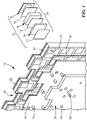
- a portion of a polarization diverse array antenna 10 (or more simply an array 10) comprises a plurality of polarization diverse radiators with a single polarization diverse radiator 12 being shown.
- Radiator 12 is comprised of a patch antenna, here a stacked-patch antenna comprising inner and outer conductors 14, 15 spaced apart by a foam spacer 16 and dielectric substrates 17, 18, 19.
- a conductive frame 20 includes walls 22 which define a plurality of apertures or cavities 24 and this frame 20 is sometime referred to as an "egg-crate frame, or metal frame” or more simply an “egg-crate.”
- Each of the plurality of radiators 12 in array 10 are disposed in a respective one of the cavities 24 provided in conductive frame 20.
- the radiator 12 and frame/cavity 20/24 together form a radiator subassembly 25.
- a substrate 26 having openings provided therein to match the lattice pattern of frame 20 is disposed between a surface of frame 20 and a surface of an integrated dilation and feed circuit 30.
- substrate 26 maybe provided as a thermal substrate, used to conduct heat between the feed subassembly and the metal frame.
- integrated dilation and feed circuit 30 may be provided as a multilayer printed circuit board (PCB).
- Radio frequency (RF) connectors 32 are coupled to dilation and feed circuit 30 and provide a means for RF signals to be coupled to/from the radiator assemblies 25 through integrated dilation and feed circuit 30.
- the RF connectors 32 are disposed through openings 34 in a support plate 36.
- Support plate 36 is disposed over a surface of dilation and feed circuit 30 opposite frame 20 to provide mechanical support to antenna 10, as well as a thermal source or sink, depending on the operating conditions.
- One or more alignment structures 38 are disposed through appropriate ones of openings in both the support plate and the integrated dilation and feed circuit 30 to aid in alignment of at least the two structures 36, 30.
- each radiator assembly 25 is coupled to a particular set of dilation and feed circuitry included in integrated dilation and feed circuit 30.
- the combination of integrated dilation and feed circuit and associated radiator assembly forms a unit cell.
- array 10 is provided from a plurality of individual polarization diverse unit cells.
- the unit cell architecture provided by the combination of radiators 12 and dilation and feed circuit 30 results in an antenna having matched unit cell insertion phases and also having physical symmetry as well as symmetric field symmetry (i.e. electromagnetic field symmetry). Having such symmetry also results in an array antenna capable of achieving a high degree of polarization isolation which is important in an antenna responsive to multiple different polarizations (i.e. a polarization diverse system).
- the combination of the radiator assembly symmetry and integrated dilation and feed circuit symmetry also results in a radiator assembly having low total and ohmic front-end loss.
- the low ohmic loss is the result of at least: minimizing the path length between the RF connector interface and the slot aperture couplers; packaging the dilation and feed networks with the maximum density while avoiding higher-order mode interaction; reducing (and ideally, minimizing) impedance mismatch at all components and their interfaces; the use of reactive, rather than resistive, combiners; and utilizing best practices in the form of the associated transmission lines e.g., conductor surface roughness, reduced (and ideally, minimum) line width allowances, and avoiding reactive field coupling.
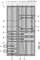
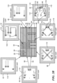
- the integrated dilation and feed circuit layer 30 includes a dilation circuit layer 44 disposed between a pair of ground plane layers 42, 46 (or more simply ground planes 42, 46).
- Dilation circuit layer 44 includes a dilation circuit 48 comprised of dilation circuit signal paths 49, 50.
- the purpose of the dilation circuits is to provide equal electrical path insertion phase for each of the two polarization and all unit cells within the array. It is noteworthy to consider that the dilation path provided differs for the various unit cells because of panel edge conditions and other unit cell differentiations. It should be appreciated that, for clarity, in Fig. 2 the inner patch element and substrate, outer patch element and substrate, cavity and integrated radome are not shown.
- a pair of dielectric substrates 52, 54 are disposed between ground planes 42, 46 and dilation circuit signal paths 49, 50 are disposed on at least one of the substrates (preferably, for at least ease of manufacturing, on the same surface of the same substrate).
- dilation circuit signal paths 49, 50 are disposed on a surface of substrate 52.
- Substrates 52, 54 are bonded or otherwise secured together.
- substrates 52, 54 are bonded via a bond film 55 (e.g. a thermoset based thin film) as is generally known.
- layers 42, 44, 46 and substrates 52, 54 provide dilation circuit as a stripline printed circuit board circuit.
- Respective ones of RF connectors 56, 58 are coupled to first ends 49a, 50a of dilation circuit signal paths 49, 50.
- Second ends 49a, 50a of signal paths 49, 50 are connected through an electrical signal path which passes through ground planes 46, 60 to a combiner circuit layer 62 disposed between a pair of ground plane layers 60, 64 (or more simply ground planes 60, 64).
- Combiner circuit layer 62 includes a pair of reactive combiner circuits 66, 68.
- second ends 49b, 50b, of signal paths 49, 50 are coupled to first ports 66a, 68a of combiner circuits 66, 68.
- interconnections 49a, 50a, 49b, 50b may all use a central conductive via with a surrounding ground via cage, forming a coaxial Transverse ElectroMagnetic (TEM) interface.
- TEM Transverse ElectroMagnetic
- a pair of dielectric substrates 72, 74 are disposed between ground planes 60, 64 and combiner circuits 66, 68 are disposed on at least one of the substrates (preferably, for ease of manufacturing, on the same surface of the same substrate, and for the purpose of creating a stripline transmission line).
- combiner circuits 66, 68 are disposed on a surface of substrate 72.
- Substrates 72, 74 are bonded or otherwise secured together.
- substrates 72, 74 are bonded via a bond film 75 (e.g. a thermoset based thin film) as is generally known.
- layers 60, 62, 64 and substrates 72, 74 provide the combiner circuit as a stripline PCB which is bonded or otherwise secured to the dilation PCB.
- the dilation and combiner PCBs are bonded via a bond film 77 (e.g. a thermoset based thin film) as is generally known.
- Second and third ports 66b, 68b, 66c, 68c of combiner circuits 66, 68 are connected through a TEM electrical signal path which passes through ground plane 64 to respective ones of feed circuits 80-86 on a feed circuit layer 78.
- second and third ports 66b, 68b, 66c, 68c of combiner circuits 66, 68 are coupled to respective ones of feed circuit ports 80a - 86a.
- combiner circuits 66, 68 are provided as reactive combiner circuits. These circuits use physical and electrical symmetry, having a significant impact on the polarization performance, and introduce transmission line impedance matching details in the form of the various stripline conductor widths, as shown.
- Feed circuit layer is disposed over a slot layer 88 having slots 90-96 provided therein.
- slot layer 88 is provided as a conductor and slots 90-96 may be formed, by etching away portions of the conductor 88. It should, of course, be appreciated, however, that any additive or subtractive process may be used to form slots (e.g. in the event that slot layer is provided as a dielectric).
- Feed circuits 80-86 are symmetrically disposed on feed layer 78 such that each feed circuit 80-86 crosses a respective one of the slots 90-96, generally denoted 97, which are symmetrically disposed on a slot layer 88.
- the feed layer 78 comprises four feed circuits 80-86.
- feed circuits may be used, and may cause degraded polarization performance.
- the feed circuits are disposed on a substrate and arranged such that when a first surface of the slot layer is disposed over a first surface of the feed layer, the feed circuits intercept (here, orthogonally cross) the slot apertures. This arrangement enables RF energy to be coupled between the slots in the slot layer and the feed circuits on the feed layer.
- These circuits use physical and electrical symmetry in the form of the four feed points used, having a significant impact on the polarization performance, and introduce central ground conductors to force electrical symmetry.
- each feed circuit is coupled to the second and third ports of reactive combiner/divider circuits provided on a combiner layer.
- the output ports of the combiner circuits are connected via an electrical signal path which passes through a ground layer and to first ends of signal paths on the dilation layer.
- the second ends of the signal paths are configured to be coupled to RF connectors.
- the feed circuits In a transmit mode of operation, the feed circuits excite the slots by means of aperture coupling. In a receive mode of operation, the feed circuits couple RF energy from the slots. The slots couple RF energy to/from (depending upon whether the system is operating in a transmit or receive mode) the radiating elements which are here provided as square patch antenna elements 14, 15 ( Fig. 1 ).
- a dielectric substrate 98 is disposed between ground plane 64 and feed circuits 80-86.
- a dielectric substrate 100 is also disposed between ground plane 64 and feed circuits 80-86 on feed layer 78.
- Feed circuits 80-86 are disposed on at least one surface of substrates 98, 100 (preferably, for ease of manufacturing, on the same surface of the same substrate).
- feed circuits 80 -86 are disposed on a surface of substrate 100.
- the feed layer 78 is configured as an asymmetric stripline circuit in order to facilitate preferred, and ideally, optimal aperture coupling between it and the slot coupler 88.
- Substrate 98 is bonded or otherwise secured to ground plane 64 and substrate 100 is bonded or otherwise secured to substrate 98.
- the substrates 98, 100 are bonded via bond films 102, 104 (e.g. a thermoset based thin film) as is generally known.
- layers 60, 62, 64 and substrates 72, 74 provide the combiner circuit as a stripline PCB circuit which is bonded or otherwise secured to the dilation PCB.
- the dilation and combiner PCBs are bonded via a bond film 77 (e.g. a so-called "thermoset" based thin film) as is generally known.
- the integrated dilation and feed circuit 30 is bi-directional meaning that RF signals may propagate in either direction through the circuit.
- signals introduced to the circuit through slot layer 88 may appear at one or both of RF connectors 56, 58 (depending upon the polarization state and the polarization phase relationship and amplitudes of the RF signals provided to the slot layer and depending upon which ones of slots 90-96 receive the signal(s)).
- signals introduced to the circuit through RF connectors 56, 58 may appear at one or all of slots 90-96 (depending upon the phase relationship and amplitudes of the RF signals provided to RF connectors 56, 58).
- RF signals are introduced into the circuit through RF connectors 56, 58 (which may correspond, for example, to a transmit mode of a radar system in which the integrated dilation and feed circuit 30 is disposed).
- RF signals propagate through connectors 56, 58 into first ends (or ports) 49a, 50a of the dilation signal paths and propagate along signal paths 49, 50 to ports 49b, 50b.
- the signals then propagate from ports 49b, 50b to inputs 66a, 68a of reactive combiners 66, 68.
- the reactive combiners divide the signals and the so-divided signals propagate from respective ones of combiner ports 66b, 66c, 68b, 68c to respective ones of feed circuit ports 80a, 82a, 84a, 86a.
- the feed circuits 80-86 are disposed such that each feed circuit substantially orthogonally intersects a respective one of the slots 90-96 and RF energy is coupled from respective ones the feed circuits 80-86 to respective ones of the slots 90-96.
- the integrated dilation and feed circuit includes a plurality of via holes.
- Via holes 110 are provided in the perimeter of each layer 42, 44, 46, 60, 62, 64 78 and 88. Via holes 110 reduce (and ideally prevent) the number and amplitude of RF signals (i.e. electromagnetic fields) from entering or leaving the unit cell (i.e. the vias 110 reduce, and ideally eliminate, leakage signals from propagating between the unit cells). The vias 110 are thus sometimes said to form an RF cage around each unit cell.
- a plurality of via holes 120 substantially encircle each of the RF ports provided in layers 42, 44, 46, 60, 62, 64 78 and 88.
- Such vias produce and ideally minimize or even eliminate stray RF signals generated, for example, as a result of TEM transitions between ports.
- dilation layer 44 is asymmetric and thus includes a large number of vias 122 to suppress any undesired electromagnetic fields (e.g. RF leakage signals) which may be generated as a result of the asymmetry. It should be appreciated that the vias 122 in dilation layer 44 do not penetrate to the combiner circuit layer, feed circuit layer or the slot layer, and are restricted to the dilation stripline circuit. Thus, the vias 122 are so-called “blind vias" since they do not extend to any visible layer of the integrated dilation and feed PCB.
- the reactive combiner circuits 66, 68 on combiner layer 62 are also asymmetric.
- a plurality of conductive via holes 112 (or more simply vias 112) are provided in the combiner layer between signal path regions 114, 115 and 116, 117 of the combiner circuits 66, 68.
- the vias 112 disposed between at least some signal paths of the combiners reduce, and ideally minimize or even totally prevent, unintentional and undesired coupling of signals (e.g. electromagnetic fields) between signal paths which make up the combiner.
- signals e.g. electromagnetic fields
- Such undesirable fields may be generated, for example, as a result of the asymmetry in the combiner circuit configuration and/or fabrication or from proximity effects of densely packed layers, such as this one.
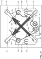
- FIG. 2C an overlay of the combiner, feed and slot layers 62, 78, 88 discussed in conjunction with Figs. 2-2B superimposed over a patch antenna element 130 is shown.
- this arrangement can be used to generate a pair of orthogonal electric field vectors 132, 134, here shown at angles of ⁇ 45° with respect to patch element 130.
- Such orthogonal electric field vectors 132, 134 may be generated when an RF signal is provided to ports 56, 58 and subsequently to ports 66a, 68a of combiner circuits 66, 68.
- the 45° vector orientation also provides orthogonal horizontal and vertical linear polarization products resulting from the 0° or 180° phase relationship between the two excited vectors.
- RF signals having any orthogonal circular polarization e.g. RF signals having left or right circular polarizations, RHCP, LHCP
- any orthogonal linear polarization e.g. RF signals having horizontal and vertical polarizations.
- those two orthogonal sets of polarization are all that is needed to detect signals (e.g. radar return signals or communication signals) having any polarization (i.e. the radar has polarization diversity).
- signals e.g. radar return signals or communication signals
- the radar has polarization diversity.
- the diagonal polarization set of fields created via the circuits and technique described herein allows the system to produce RHCP, LHCP as well as horizontal and vertical polarizations with full radiated power, other than the orthogonal diagonal polarizations, these latter being considered unnecessary for radar operation.
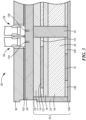
- a unit cell portion 62 of an array antenna 10' which may be the same as or similar to array antenna 10 describe above in conjunction with Fig. 1 , includes support plate 36 having a pair of connectors 56, 58 disposed there through.
- a gap pad 132 is disposed between a surface of support plate 36 and a surface of integrated dilation and feed circuit 30. Gap pad 132 has a thickness and pliability characteristic sufficient to fill gaps between the surfaces of support plate 36 and a surface of integrated dilation and feed circuit 30 (e.g.
- Center conductors (or pins) 134, 136 of RF connectors 56, 58 extend into integrated dilation and feed circuit 30 and provide an RF connect to dilation signal path ports 49a, 50a ( Fig. 2 ).
- the center conductors of the RF connectors extend through dilation and combiner layers 44, 62 but do not extend to feed circuit layer 78.
- Integrated dilation and feed circuit 30 is disposed on a first surface of frame 20 and more particularly on surfaces of frame walls 22.
- Substrate 17 is disposed over a surface of dilation and feed circuit 30 and inner patch 14 is disposed over substrate 17.
- a substrate 18 is disposed over patch 14.
- Substrates 17, 18 are bonded or otherwise screwed together e.g. via bond film 137 (e.g. a thermostat based thing film) as is generally known.
- Foam spacer 16 is disposed between outer patch 15 and dielectric substrate 18.
- a radome 138 is disposed over outer patch 15.
- a bond film 139 secures the radome 138 to foam spacer 16 to thus provide radome 138 as an integrated radome.
- RF energy is coupled through RF connectors 56, 58 and into dilation and feed circuit 30.
- the RF energy propagates through dilation and feed circuit 30 to slots (or apertures) 90-96 and into the radiator cavity 24 ( Fig. 1 ) to the dual-polarized, stacked-patch antenna elements 14, 15.
- RF energy intercepted by the dual stacked-patch antenna elements 14, 15 is coupled into the cavity 24 defined by conductive walls 22 and subsequently through the apertures 90-96 in the slot layer 88 ( Fig. 2 ) to feed circuitry, combiner circuitry and dilation circuitry through which the signals are coupled to RF connectors 56, 58.
- RF signals having two orthogonal polarizations are provided at respective ones of the RF connectors 56, 58.
- the two patches 14, 15, as well as slot and feed layers 88, 78 are provided having as close to perfect physical symmetry as possible.
- Such symmetry provides the radiator assembly having a relatively high cross-polarization characteristic, given the electrical symmetry of the feed circuitry.
- a polarization diverse active electronically scanned array (AESA) 140 is provided from a plurality of polarization diverse radiators, which maybe the same as or similar to the radiators described above in conjunction with Figs. 1-3 .
- each "block" 142 shown in Fig. 4 represents a unit cell which may be the same as or similar to the unit cells described above in conjunction with Figs. 1-3 .
- the radiators and more particularly the unit cells 142 which make up AESA 140 are disposed in a triangular lattice configuration.
- the polarization diverse radiators may be the same as or similar to the radiators described above in conjunction with Figs. 1-3 and are responsive to RF signals having both orthogonal circular and orthogonal linear polarizations.
- the AESA is sequentially responsive to RF signals having orthogonal circular and linear polarizations.
- the AESA is simultaneously response to orthogonal circular and linearly polarized RF signals.
- the AESA 140 is comprised of a plurality of panels, here four panels 142-148, each of which is provided from a plurality of polarization diverse elements included in unit cells 142. It should be appreciated that in this exemplary embodiment, the total number of unit cells 142 comprises the entire array antenna 140. In one embodiment, the total number of unit cells is sixteen. The particular number of unit cells used to provide a complete AESA antenna can be selected in accordance with a variety of factors including, but not limited to, the frequency of operation, array gain, the space available for the array antenna and the particular application for which array antenna 140 is intended to be used.
- unit cells 142 may be grouped into sub-arrays. Those of ordinary skill will also appreciate how to select the number of unit cells included in each sub-array as well as the number of sub-arrays to include in each panel which comprise the complete AESA antenna.
- each panel comprises twelve rows 153a - 153l of antenna elements with each row containing twelve unit cells (and thus twelve radiator assemblies).
- Each of the panels is thus said to be a twelve by twelve (or 12x12) panel.
- Other panel sizes and configurations are also possible (e.g. eight by eight panels or rectangular or triangular shaped panels).
- each panel comprises one hundred forty-four (144) unit cells.
- the array 140 comprises a total of five-hundred and seventy-six (576) unit cells.
- each panel can include any desired number of elements.
- the particular number of elements to include in each of the panels can be selected in accordance with a variety of factors, including but not limited to, the desired frequency of operation, array gain, the space available for array antenna 140 and the particular application for which the array antenna 140 is intended to be used as well as the size of each panel.
- those of ordinary skill in the art will appreciate how to select an appropriate number of radiating elements to include in each panel and/or in the array 140.
- the total number of unit cells 142 included in an antenna array such as antenna array 140 depends upon the number of panels included in the antenna array and the number of antenna elements included in each panel.
- each unit cell may be electrically autonomous (excepting of course any mutual coupling which occurs between elements within a panel and on different panels).
- the RF feed circuitry which couples RF energy to and from each radiator on a panel is incorporated entirely within the unit cell for that radiator (i.e. all of the RF feed circuitry which couples RF signals to and from an antenna element is contained within that element).
- each unit cell includes one or more RF connectors and the RF signals are provided to/from the antenna element through the RF connector(s) provided on each unit cell.
- signal paths for logic signals and signal paths for power signals which couple signals to and from transmit/receive (T/R) circuits are contained within the panel in which the TRIMM modules exist.
- An RF beam for the entire array 140 is formed by an internal or external beamformer (i.e. external to each of the unit cells or to their panel assembly) that combines the RF outputs from each of the unit cells.
- the beamformer may be conventionally implemented as a printed wiring board (e.g. a stripline circuit) that combines N elements into one RF signal port (and hence the beamformer may be referred to as a 1:N beamformer).
- the elements are mechanically fastened or otherwise secured to a mounting structure (e.g. support plate 36 in Fig. 1 ) using conventional techniques such that the array lattice pattern is continuous across each panel which comprises the array antenna.
- the mounting structure may be provided as a "picture frame" to which the elements are secured using fasteners.
- the tolerance between interlocking sections of the panels is selected based upon a variety of factors including but not limited to the frequency of operation and the affect of the tolerance on antenna performance.
- antennas operating in K-band frequency range may require tighter (i.e. smaller) tolerances than antennas operating in the S-band frequency range, for example.
- the elements are mechanically mounted such that the array lattice pattern (which is shown as a triangular lattice pattern in exemplary embodiment of Fig. 4 ) appears electrically continuous across the entire surface (or "face") of the array 140.
- circuits, systems and techniques described herein may include one or more of the features and/or structures describe above in conjunction with Figs. 1-4 and that the features and/or structures may be used independently or in combination with one or more other features and/or structures and that features and/or structures of different embodiments described herein may be combined to form other embodiments which may not be specifically set forth herein.
Landscapes
- Variable-Direction Aerials And Aerial Arrays (AREA)
- Waveguide Aerials (AREA)
Claims (15)
- Circuit intégré de dilatation et d'alimentation (30) comprenant :une couche de dilatation asymétrique (44) comprenant une paire de chemins de signal de circuit de dilatation ;une couche de combineur réactif asymétrique (62) comprenant une paire de circuits de combineur réactif, ladite couche de circuits de combineur réactif asymétrique étant disposée sur ladite couche de dilatation asymétrique de telle sorte que ladite paire de circuits de combineur réactif soit couplée à des chemins de signaux respectifs de ladite paire de chemins de signal de circuit de dilatation ;une couche d'alimentation symétrique (78) ayant une pluralité de circuits d'alimentation disposés symétriquement sur celle-ci ; ladite couche d'alimentation symétrique étant disposée sur ladite couche de combineur réactif asymétrique de sorte que chacun de ladite pluralité de circuits d'alimentation disposés symétriquement est couplé à l'un de ladite paire de circuits de combineur réactif asymétrique ; ladite couche d'alimentation symétrique étant configurée pour être à la fois physiquement et électriquement symétrique ; etune couche de fentes symétriques (88) ayant une pluralité similaire de fentes disposées symétriquement sur celle-ci, ladite couche de fentes symétriques étant disposée sur ladite couche d'alimentation symétrique de sorte que chacun de ladite pluralité de circuits d'alimentation coupe une fente respective de ladite pluralité de fentes, ladite couche de fentes symétriques étant configurée pour être à la fois physiquement et électriquement symétrique.
- Circuit intégré de dilatation et d'alimentation selon la revendication 1, comprenant en outre :une paire de substrats, chacun ayant des première et seconde surfaces opposées ;une paire de plans de masse disposés sur des premières surfaces correspondantes de ladite paire de substrats ; et,ladite couche de dilatation asymétrique étant disposée sur une seconde surface d'un substrat opposé au plan de masse ; ouladite couche de combineur réactif asymétrique étant disposée sur une seconde surface d'un substrat opposé au plan de masse ; ouladite couche d'alimentation symétrique étant disposée sur une seconde surface d'un substrat opposé au plan de masse.
- Circuit intégré de dilatation et d'alimentation selon la revendication 1,ladite couche de fentes étant prévue comme une couche conductrice ayant des fentes prévues dans celle-ci ; ouladite couche de fentes symétriques étant prévue comme une couche conductrice ayant des fentes symétriques prévues dans celle-ci ; ouladite pluralité de circuits d'alimentation croisant symétriquement une fente respective de ladite pluralité de fentes symétriques.
- Circuit intégré de dilatation et d'alimentation selon la revendication 2 comprenant en outre une paire de connecteurs de radiofréquence, RF, disposés sur l'un de ladite paire de plans de masse avec un premier de ladite paire de connecteurs RF et couplé à une première extrémité d'un premier de ladite paire de chemins de signal de circuit de dilatation et un second de ladite paire de connecteurs RF couplé à une première extrémité d'un second de ladite paire de chemins de signal de circuit de dilatation.
- Circuit intégré de dilatation et d'alimentation selon la revendication 1, comprenant en outre :une première paire de substrats, chacun ayant des première et seconde surfaces opposées et une première paire de plans de masse disposés sur des premières surfaces correspondantes de ladite première paire de substrats, ledit circuit de dilatation asymétrique étant disposé sur une seconde surface d'un substrat de ladite première paire de substrats opposée au plan de masse ;une deuxième paire de substrats disposés sur ladite première paire de substrats, chacun de ladite deuxième paire de substrats ayant des première et seconde surfaces opposées et une deuxième paire de plans de masse disposés sur des premières surfaces correspondantes de ladite deuxième paire de substrats, ladite couche de combineur réactif asymétrique étant disposée sur une seconde surface d'un substrat de ladite deuxième paire de substrats opposée au plan de masse ;une troisième paire de substrats ayant chacun des première et seconde surfaces opposées, ladite troisième paire de substrats étant disposée sur ladite deuxième paire de substrats de telle sorte qu'une première surface d'un premier substrat de ladite troisième paire de substrats est disposée sur l'un de la deuxième paire de plans de masse, et ladite couche d'alimentation symétrique étant disposée sur une seconde surface d'un substrat de ladite troisième paire de substrats ; etladite couche de fentes étant prévue comme une couche conductrice disposée sur une surface du second substrat de ladite troisième paire de substrats.
- Circuit intégré de dilatation et d'alimentation selon la revendication 1, comprenant en outre une pluralité de trous d'interconnexion conducteurs prévus dans ladite deuxième paire de substrats et ladite couche de combineur réactif asymétrique, lesdits trous d'interconnexion conducteurs s'étendant entre la deuxième paire de plans de masse, ladite pluralité de trous d'interconnexion conducteurs étant disposée entre les chemins de signaux de ladite paire de circuits de combineur réactif.
- Circuit intégré de dilatation et d'alimentation selon la revendication 6, comprenant en outre une pluralité de trous d'interconnexion conducteurs prévus dans ladite couche de dilatation et disposées à travers ladite couche de dilatation pour supprimer les champs électromagnétiques indésirables dans ladite couche de dilatation.
- Circuit intégré de dilatation et d'alimentation selon la revendication 1, chacun de ladite pluralité de circuits d'alimentation croisant symétriquement une fente respective de ladite pluralité de fentes symétriques.
- Antenne à polarisation diverse comprenant :un circuit intégré de dilatation et d'alimentation selon n'importe quelle revendication précédente ; etun ensemble de radiateurs comprenant au moins un radiateur, ledit ensemble de radiateurs étant disposé sur ledit circuit intégré de dilatation et d'alimentation de sorte que les fentes dans ladite couche de fentes symétriques sont disposées pour coupler les signaux RF entre au moins un radiateur et ladite pluralité de circuits d'alimentation symétriques.
- Antenne selon la revendication 9, ladite pluralité de circuits d'alimentation :étant disposés sur un substrat de telle sorte que lorsqu'une première surface de la couche de fentes est disposée sur une première surface de la couche d'alimentation, ladite pluralité de circuits d'alimentation croise orthogonalement des ouvertures respectives de ladite pluralité d'ouvertures de fentes de telle sorte que l'énergie RF puisse être couplée entre les fentes dans ladite couche de fentes et les circuits d'alimentation sur ladite couche d'alimentation ; oucorrespondant à quatre circuits d'alimentation et ladite pluralité de fentes correspondant à quatre fentes diagonales, et les circuits respectifs desdits quatre circuits d'alimentation croisant les fentes respectives desdites quatre fentes.
- Antenne selon la revendication 10, l'ensemble de radiateurs comprenant :un cadre conducteur ayant des parois qui définissent une cavité ; etun radiateur disposé dans la cavité.
- Antenne selon la revendication 11, ledit radiateur étant fourni comme un élément d'antenne à plaque ;éventuellement, ladite antenne à plaque étant fournie sous la forme d'une antenne à plaque empilée symétrique comprenant des conducteurs internes et externes espacés par une entretoise en mousse et des substrats diélectriques ; etéventuellement, lesdites couches de combineur, d'alimentation et de fente étant disposées par rapport audit élément d'antenne à plaque de manière à générer une paire de vecteurs de champ électrique orthogonaux par rapport audit élément à plaque.
- Antenne selon la revendication 9, comprenant en outre :une première pluralité de trous d'interconnexion conducteurs prévus dans le périmètre de chacune desdites couche de dilatation asymétrique, couche de combineur réactif asymétrique, couche d'alimentation symétrique et couche de fentes symétriques de façon à former une cage RF dans le circuit intégré de dilatation et d'alimentation ;une deuxième pluralité de trous d'interconnexion conducteurs prévues dans ladite couche de dilatation et disposées dans toute ladite couche de dilatation pour supprimer les champs électromagnétiques indésirables dans ladite couche de dilatation, ladite deuxième pluralité de trous d'interconnexion conducteurs ne pénétrant pas dans ladite couche de circuit de combineur, ladite couche de circuit d'alimentation ou ladite couche de fente ; etune troisième pluralité de trous d'interconnexion conducteurs prévus dans ladite couche de combineur réactif asymétrique entre des régions de chemin de signal de ladite paire de circuits de combineur réactif asymétrique.
- Réseau à balayage électronique actif, AESA, comprenant :un cadre en forme de coquille d'oeuf ayant une pluralité de parois électriquement conductrices qui définissent une pluralité de cavités ; etune pluralité de radiateurs à polarisation diverse, chacun desdits radiateurs à polarisation diverse étant disposé à l'intérieur de l'une de la pluralité de cavités dans ledit cadre en forme de coquille d'œuf, chacun de ladite pluralité de radiateurs à polarisation diverse comprenant :un élément d'antenne interne fourni à partir d'un ou plusieurs substrats sur lesquels est disposé un conducteur, chacun du ou des substrats de l'élément d'antenne interne ayant des dimensions telles que ledit élément d'antenne s'adapte à l'intérieur de la cavité ;un élément d'antenne externe fourni à partir d'un ou plusieurs substrats sur lesquels est disposé un conducteur, lesdits un ou plusieurs substrats d'élément d'antenne externe ayant sensiblement les mêmes dimensions que le ou les substrats d'élément d'antenne interne ; etune entretoise diélectrique disposée entre les éléments d'antenne internes et externes, ladite entretoise diélectrique ayant sensiblement les mêmes dimensions que le ou les substrats d'éléments d'antenne internes et externes ; etun circuit intégré de dilatation et d'alimentation disposé sur et couplé à ladite pluralité de radiateurs à polarisation diverse, ledit circuit intégré de dilatation et d'alimentation comprenant les circuits selon l'une quelconque des revendications 1 à 8, chacun de ladite pluralité de circuits d'alimentation coupant une fente respective de ladite pluralité de fentes de sorte que les fentes dans ladite couche de fentes symétriques sont disposées pour coupler des signaux RF entre la pluralité de radiateurs à polarisation diverse et ladite couche d'alimentation symétrique.
- Réseau à balayage électronique actif, AESA, selon la revendication 14, chacun des éléments d'antenne internes et des éléments d'antenne externes étant disposés pour fournir des éléments d'antenne à plaque empilés symétriques, chacun desdits éléments d'antenne à plaque empilés étant disposé symétriquement à l'intérieur d'une cavité respective de la pluralité de cavités ; facultativementles fentes dans la couche de fentes symétriques correspondant à des coupleurs à ouverture fendue, chacun des coupleurs à ouverture fendue ayant une orientation qui est configurée pour fournir un transfert de puissance complet pour des polarisations circulaires orthogonales et des polarisations horizontales et verticales ; etfacultativement, les coupleurs à ouverture fendue étant fournis avec une orientation de 45 degrés de sorte que les coupleurs à ouverture fendue fournissent un transfert de puissance complet pour les champs électriques ayant au moins l'une des polarisations suivantes : des polarisations circulaires orthogonales ;une polarisation horizontale ; et une polarisation verticale.
Applications Claiming Priority (2)
| Application Number | Priority Date | Filing Date | Title |
|---|---|---|---|
| US14/999,923 US12362499B1 (en) | 2016-12-16 | 2016-12-16 | Polarization versatile radiator |
| PCT/US2017/066359 WO2018112175A1 (fr) | 2016-12-16 | 2017-12-14 | Radiateur polyvalent à polarisation |
Publications (2)
| Publication Number | Publication Date |
|---|---|
| EP3555962A1 EP3555962A1 (fr) | 2019-10-23 |
| EP3555962B1 true EP3555962B1 (fr) | 2023-03-15 |
Family
ID=60937916
Family Applications (1)
| Application Number | Title | Priority Date | Filing Date |
|---|---|---|---|
| EP17826059.2A Active EP3555962B1 (fr) | 2016-12-16 | 2017-12-14 | Radiateur polyvalent à polarisation |
Country Status (4)
| Country | Link |
|---|---|
| US (1) | US12362499B1 (fr) |
| EP (1) | EP3555962B1 (fr) |
| JP (1) | JP6896860B2 (fr) |
| WO (1) | WO2018112175A1 (fr) |
Families Citing this family (4)
| Publication number | Priority date | Publication date | Assignee | Title |
|---|---|---|---|---|
| CN110797654B (zh) * | 2019-12-03 | 2025-04-25 | 惠州硕贝德无线科技股份有限公司 | 一种同频带间高隔离度天线及微基站 |
| CN111856407B (zh) * | 2020-06-11 | 2023-09-29 | 南京吉凯微波技术有限公司 | 星载有源相控阵雷达x波段双极化高隔离度微波tr组件 |
| CN113851830B (zh) * | 2021-10-13 | 2023-05-30 | 中国电子科技集团公司第三十八研究所 | 一种轻质多单元天线振子及生产方法 |
| TWM661993U (zh) * | 2024-06-04 | 2024-10-21 | 廣達電腦股份有限公司 | 天線系統 |
Citations (2)
| Publication number | Priority date | Publication date | Assignee | Title |
|---|---|---|---|---|
| US20100117917A1 (en) * | 2008-11-12 | 2010-05-13 | Kindt Rickie W | Wavelength-scaled ultra-wideband antenna array |
| US9614290B1 (en) * | 2015-12-03 | 2017-04-04 | Raytheon Company | Expanding lattice notch array antenna |
Family Cites Families (22)
| Publication number | Priority date | Publication date | Assignee | Title |
|---|---|---|---|---|
| US5268701A (en) * | 1992-03-23 | 1993-12-07 | Raytheon Company | Radio frequency antenna |
| US5786792A (en) * | 1994-06-13 | 1998-07-28 | Northrop Grumman Corporation | Antenna array panel structure |
| JP3468044B2 (ja) | 1997-08-19 | 2003-11-17 | 三菱電機株式会社 | 平面アンテナ |
| US6005531A (en) * | 1998-09-23 | 1999-12-21 | Northrop Grumman Corporation | Antenna assembly including dual channel microwave transmit/receive modules |
| JP2000261235A (ja) | 1999-03-05 | 2000-09-22 | Mitsubishi Electric Corp | トリプレート線路給電型マイクロストリップアンテナ |
| US6507320B2 (en) | 2000-04-12 | 2003-01-14 | Raytheon Company | Cross slot antenna |
| US6542048B1 (en) | 2000-04-13 | 2003-04-01 | Raytheon Company | Suspended transmission line with embedded signal channeling device |
| US6624787B2 (en) * | 2001-10-01 | 2003-09-23 | Raytheon Company | Slot coupled, polarized, egg-crate radiator |
| US6611180B1 (en) | 2002-04-16 | 2003-08-26 | Raytheon Company | Embedded planar circulator |
| US6731189B2 (en) | 2002-06-27 | 2004-05-04 | Raytheon Company | Multilayer stripline radio frequency circuits and interconnection methods |
| US20060038732A1 (en) * | 2003-07-11 | 2006-02-23 | Deluca Mark R | Broadband dual polarized slotline feed circuit |
| JP4404797B2 (ja) | 2005-03-29 | 2010-01-27 | 京セラ株式会社 | 配線基板 |
| US7671696B1 (en) * | 2006-09-21 | 2010-03-02 | Raytheon Company | Radio frequency interconnect circuits and techniques |
| US8279131B2 (en) | 2006-09-21 | 2012-10-02 | Raytheon Company | Panel array |
| GB0811990D0 (en) * | 2008-07-01 | 2008-08-06 | Dockon Ltd | Improvements in and relating to radio frequency combiners/splitters |
| US8350773B1 (en) * | 2009-06-03 | 2013-01-08 | The United States Of America, As Represented By The Secretary Of The Navy | Ultra-wideband antenna element and array |
| US8814601B1 (en) * | 2011-06-06 | 2014-08-26 | Nuvotronics, Llc | Batch fabricated microconnectors |
| US8736505B2 (en) * | 2012-02-21 | 2014-05-27 | Ball Aerospace & Technologies Corp. | Phased array antenna |
| US9225070B1 (en) | 2012-10-01 | 2015-12-29 | Lockheed Martin Corporation | Cavity backed aperture coupled dielectrically loaded waveguide radiating element with even mode excitation and wide angle impedance matching |
| US9520655B2 (en) * | 2014-05-29 | 2016-12-13 | University Corporation For Atmospheric Research | Dual-polarized radiating patch antenna |
| US9806432B2 (en) * | 2015-12-02 | 2017-10-31 | Raytheon Company | Dual-polarized wideband radiator with single-plane stripline feed |
| US9979097B2 (en) * | 2016-03-16 | 2018-05-22 | Raytheon Company | Expanding lattice notch array antenna and method of fabrication |
-
2016
- 2016-12-16 US US14/999,923 patent/US12362499B1/en active Active
-
2017
- 2017-12-14 JP JP2019531935A patent/JP6896860B2/ja active Active
- 2017-12-14 WO PCT/US2017/066359 patent/WO2018112175A1/fr not_active Ceased
- 2017-12-14 EP EP17826059.2A patent/EP3555962B1/fr active Active
Patent Citations (2)
| Publication number | Priority date | Publication date | Assignee | Title |
|---|---|---|---|---|
| US20100117917A1 (en) * | 2008-11-12 | 2010-05-13 | Kindt Rickie W | Wavelength-scaled ultra-wideband antenna array |
| US9614290B1 (en) * | 2015-12-03 | 2017-04-04 | Raytheon Company | Expanding lattice notch array antenna |
Also Published As
| Publication number | Publication date |
|---|---|
| EP3555962A1 (fr) | 2019-10-23 |
| JP6896860B2 (ja) | 2021-06-30 |
| US12362499B1 (en) | 2025-07-15 |
| JP2020524920A (ja) | 2020-08-20 |
| WO2018112175A1 (fr) | 2018-06-21 |
Similar Documents
| Publication | Publication Date | Title |
|---|---|---|
| CA2884886C (fr) | Element rayonnant en plaque a polarisation lineaire double et circulaire | |
| EP3384558B1 (fr) | Radiateur à large bande à double polarisation avec alimentation à micro-ruban à plan unique | |
| US10424847B2 (en) | Wideband dual-polarized current loop antenna element | |
| US6232920B1 (en) | Array antenna having multiple independently steered beams | |
| US9455500B1 (en) | Phase center coincident, dual-polarization BAVA radiating elements for UWB ESA apertures | |
| US9225070B1 (en) | Cavity backed aperture coupled dielectrically loaded waveguide radiating element with even mode excitation and wide angle impedance matching | |
| EP2575213B1 (fr) | Réseau d'antennes à double polarisation et double phase à large bande et grande capacité de balayage | |
| US7532171B2 (en) | Millimeter wave electronically scanned antenna | |
| US20030122724A1 (en) | Planar array antenna | |
| JP2010514373A (ja) | フェーズドアレイアンテナ装置およびその製造方法 | |
| US10741901B2 (en) | Low-profile stacked patch radiator with integrated heating circuit | |
| JP6896860B2 (ja) | 偏波多用途ラジエータ | |
| EP4305709B1 (fr) | Interface de carte de circuit imprimé orthogonale | |
| US20060273973A1 (en) | Millimeter wave passive electronically scanned antenna | |
| US12537314B2 (en) | Active phased array with integrated antennas and circuits on common printed circuit cards | |
| US12394913B1 (en) | Planar dual-polarization antenna | |
| CN119965552B (zh) | 一种宽带双圆极化天线单元及阵列 | |
| US20260142377A1 (en) | Compact radiation pattern decoupling design of two-dimensional mimo microstrip antennas | |
| Koul et al. | Gain Switchable Antenna Modules | |
| CN121642528A (zh) | 基于微带腔体的四端口相模天线及其大角度扫描阵列 | |
| CN121840178A (zh) | 一种天线单元以及通信设备 |
Legal Events
| Date | Code | Title | Description |
|---|---|---|---|
| STAA | Information on the status of an ep patent application or granted ep patent |
Free format text: STATUS: UNKNOWN |
|
| STAA | Information on the status of an ep patent application or granted ep patent |
Free format text: STATUS: THE INTERNATIONAL PUBLICATION HAS BEEN MADE |
|
| PUAI | Public reference made under article 153(3) epc to a published international application that has entered the european phase |
Free format text: ORIGINAL CODE: 0009012 |
|
| STAA | Information on the status of an ep patent application or granted ep patent |
Free format text: STATUS: REQUEST FOR EXAMINATION WAS MADE |
|
| 17P | Request for examination filed |
Effective date: 20190628 |
|
| AK | Designated contracting states |
Kind code of ref document: A1 Designated state(s): AL AT BE BG CH CY CZ DE DK EE ES FI FR GB GR HR HU IE IS IT LI LT LU LV MC MK MT NL NO PL PT RO RS SE SI SK SM TR |
|
| AX | Request for extension of the european patent |
Extension state: BA ME |
|
| RIN1 | Information on inventor provided before grant (corrected) |
Inventor name: SCHUSS, JACK, J. Inventor name: SIKINA, THOMAS, V. Inventor name: ISOM, ROBERT, S. Inventor name: FURMAN, IZABELLA |
|
| DAV | Request for validation of the european patent (deleted) | ||
| DAX | Request for extension of the european patent (deleted) | ||
| GRAP | Despatch of communication of intention to grant a patent |
Free format text: ORIGINAL CODE: EPIDOSNIGR1 |
|
| STAA | Information on the status of an ep patent application or granted ep patent |
Free format text: STATUS: GRANT OF PATENT IS INTENDED |
|
| INTG | Intention to grant announced |
Effective date: 20211112 |
|
| GRAJ | Information related to disapproval of communication of intention to grant by the applicant or resumption of examination proceedings by the epo deleted |
Free format text: ORIGINAL CODE: EPIDOSDIGR1 |
|
| STAA | Information on the status of an ep patent application or granted ep patent |
Free format text: STATUS: REQUEST FOR EXAMINATION WAS MADE |
|
| INTC | Intention to grant announced (deleted) | ||
| GRAP | Despatch of communication of intention to grant a patent |
Free format text: ORIGINAL CODE: EPIDOSNIGR1 |
|
| STAA | Information on the status of an ep patent application or granted ep patent |
Free format text: STATUS: GRANT OF PATENT IS INTENDED |
|
| INTG | Intention to grant announced |
Effective date: 20220921 |
|
| GRAS | Grant fee paid |
Free format text: ORIGINAL CODE: EPIDOSNIGR3 |
|
| GRAA | (expected) grant |
Free format text: ORIGINAL CODE: 0009210 |
|
| STAA | Information on the status of an ep patent application or granted ep patent |
Free format text: STATUS: THE PATENT HAS BEEN GRANTED |
|
| AK | Designated contracting states |
Kind code of ref document: B1 Designated state(s): AL AT BE BG CH CY CZ DE DK EE ES FI FR GB GR HR HU IE IS IT LI LT LU LV MC MK MT NL NO PL PT RO RS SE SI SK SM TR |
|
| REG | Reference to a national code |
Ref country code: CH Ref legal event code: EP Ref country code: GB Ref legal event code: FG4D |
|
| REG | Reference to a national code |
Ref country code: DE Ref legal event code: R096 Ref document number: 602017066872 Country of ref document: DE |
|
| REG | Reference to a national code |
Ref country code: IE Ref legal event code: FG4D |
|
| REG | Reference to a national code |
Ref country code: AT Ref legal event code: REF Ref document number: 1554530 Country of ref document: AT Kind code of ref document: T Effective date: 20230415 |
|
| REG | Reference to a national code |
Ref country code: NO Ref legal event code: T2 Effective date: 20230315 |
|
| REG | Reference to a national code |
Ref country code: LT Ref legal event code: MG9D |
|
| P01 | Opt-out of the competence of the unified patent court (upc) registered |
Effective date: 20230530 |
|
| REG | Reference to a national code |
Ref country code: NL Ref legal event code: MP Effective date: 20230315 |
|
| PG25 | Lapsed in a contracting state [announced via postgrant information from national office to epo] |
Ref country code: RS Free format text: LAPSE BECAUSE OF FAILURE TO SUBMIT A TRANSLATION OF THE DESCRIPTION OR TO PAY THE FEE WITHIN THE PRESCRIBED TIME-LIMIT Effective date: 20230315 Ref country code: LV Free format text: LAPSE BECAUSE OF FAILURE TO SUBMIT A TRANSLATION OF THE DESCRIPTION OR TO PAY THE FEE WITHIN THE PRESCRIBED TIME-LIMIT Effective date: 20230315 Ref country code: LT Free format text: LAPSE BECAUSE OF FAILURE TO SUBMIT A TRANSLATION OF THE DESCRIPTION OR TO PAY THE FEE WITHIN THE PRESCRIBED TIME-LIMIT Effective date: 20230315 Ref country code: HR Free format text: LAPSE BECAUSE OF FAILURE TO SUBMIT A TRANSLATION OF THE DESCRIPTION OR TO PAY THE FEE WITHIN THE PRESCRIBED TIME-LIMIT Effective date: 20230315 |
|
| REG | Reference to a national code |
Ref country code: AT Ref legal event code: MK05 Ref document number: 1554530 Country of ref document: AT Kind code of ref document: T Effective date: 20230315 |
|
| PG25 | Lapsed in a contracting state [announced via postgrant information from national office to epo] |
Ref country code: SE Free format text: LAPSE BECAUSE OF FAILURE TO SUBMIT A TRANSLATION OF THE DESCRIPTION OR TO PAY THE FEE WITHIN THE PRESCRIBED TIME-LIMIT Effective date: 20230315 Ref country code: NL Free format text: LAPSE BECAUSE OF FAILURE TO SUBMIT A TRANSLATION OF THE DESCRIPTION OR TO PAY THE FEE WITHIN THE PRESCRIBED TIME-LIMIT Effective date: 20230315 Ref country code: GR Free format text: LAPSE BECAUSE OF FAILURE TO SUBMIT A TRANSLATION OF THE DESCRIPTION OR TO PAY THE FEE WITHIN THE PRESCRIBED TIME-LIMIT Effective date: 20230616 Ref country code: FI Free format text: LAPSE BECAUSE OF FAILURE TO SUBMIT A TRANSLATION OF THE DESCRIPTION OR TO PAY THE FEE WITHIN THE PRESCRIBED TIME-LIMIT Effective date: 20230315 |
|
| PG25 | Lapsed in a contracting state [announced via postgrant information from national office to epo] |
Ref country code: SM Free format text: LAPSE BECAUSE OF FAILURE TO SUBMIT A TRANSLATION OF THE DESCRIPTION OR TO PAY THE FEE WITHIN THE PRESCRIBED TIME-LIMIT Effective date: 20230315 Ref country code: RO Free format text: LAPSE BECAUSE OF FAILURE TO SUBMIT A TRANSLATION OF THE DESCRIPTION OR TO PAY THE FEE WITHIN THE PRESCRIBED TIME-LIMIT Effective date: 20230315 Ref country code: PT Free format text: LAPSE BECAUSE OF FAILURE TO SUBMIT A TRANSLATION OF THE DESCRIPTION OR TO PAY THE FEE WITHIN THE PRESCRIBED TIME-LIMIT Effective date: 20230717 Ref country code: ES Free format text: LAPSE BECAUSE OF FAILURE TO SUBMIT A TRANSLATION OF THE DESCRIPTION OR TO PAY THE FEE WITHIN THE PRESCRIBED TIME-LIMIT Effective date: 20230315 Ref country code: EE Free format text: LAPSE BECAUSE OF FAILURE TO SUBMIT A TRANSLATION OF THE DESCRIPTION OR TO PAY THE FEE WITHIN THE PRESCRIBED TIME-LIMIT Effective date: 20230315 Ref country code: CZ Free format text: LAPSE BECAUSE OF FAILURE TO SUBMIT A TRANSLATION OF THE DESCRIPTION OR TO PAY THE FEE WITHIN THE PRESCRIBED TIME-LIMIT Effective date: 20230315 Ref country code: AT Free format text: LAPSE BECAUSE OF FAILURE TO SUBMIT A TRANSLATION OF THE DESCRIPTION OR TO PAY THE FEE WITHIN THE PRESCRIBED TIME-LIMIT Effective date: 20230315 |
|
| PG25 | Lapsed in a contracting state [announced via postgrant information from national office to epo] |
Ref country code: SK Free format text: LAPSE BECAUSE OF FAILURE TO SUBMIT A TRANSLATION OF THE DESCRIPTION OR TO PAY THE FEE WITHIN THE PRESCRIBED TIME-LIMIT Effective date: 20230315 Ref country code: PL Free format text: LAPSE BECAUSE OF FAILURE TO SUBMIT A TRANSLATION OF THE DESCRIPTION OR TO PAY THE FEE WITHIN THE PRESCRIBED TIME-LIMIT Effective date: 20230315 Ref country code: IS Free format text: LAPSE BECAUSE OF FAILURE TO SUBMIT A TRANSLATION OF THE DESCRIPTION OR TO PAY THE FEE WITHIN THE PRESCRIBED TIME-LIMIT Effective date: 20230715 |
|
| REG | Reference to a national code |
Ref country code: DE Ref legal event code: R097 Ref document number: 602017066872 Country of ref document: DE |
|
| PLBE | No opposition filed within time limit |
Free format text: ORIGINAL CODE: 0009261 |
|
| STAA | Information on the status of an ep patent application or granted ep patent |
Free format text: STATUS: NO OPPOSITION FILED WITHIN TIME LIMIT |
|
| PG25 | Lapsed in a contracting state [announced via postgrant information from national office to epo] |
Ref country code: SI Free format text: LAPSE BECAUSE OF FAILURE TO SUBMIT A TRANSLATION OF THE DESCRIPTION OR TO PAY THE FEE WITHIN THE PRESCRIBED TIME-LIMIT Effective date: 20230315 Ref country code: DK Free format text: LAPSE BECAUSE OF FAILURE TO SUBMIT A TRANSLATION OF THE DESCRIPTION OR TO PAY THE FEE WITHIN THE PRESCRIBED TIME-LIMIT Effective date: 20230315 |
|
| 26N | No opposition filed |
Effective date: 20231218 |
|
| PG25 | Lapsed in a contracting state [announced via postgrant information from national office to epo] |
Ref country code: IT Free format text: LAPSE BECAUSE OF FAILURE TO SUBMIT A TRANSLATION OF THE DESCRIPTION OR TO PAY THE FEE WITHIN THE PRESCRIBED TIME-LIMIT Effective date: 20230315 |
|
| REG | Reference to a national code |
Ref country code: CH Ref legal event code: PL |
|
| PG25 | Lapsed in a contracting state [announced via postgrant information from national office to epo] |
Ref country code: LU Free format text: LAPSE BECAUSE OF NON-PAYMENT OF DUE FEES Effective date: 20231214 |
|
| PG25 | Lapsed in a contracting state [announced via postgrant information from national office to epo] |
Ref country code: MC Free format text: LAPSE BECAUSE OF FAILURE TO SUBMIT A TRANSLATION OF THE DESCRIPTION OR TO PAY THE FEE WITHIN THE PRESCRIBED TIME-LIMIT Effective date: 20230315 |
|
| REG | Reference to a national code |
Ref country code: BE Ref legal event code: MM Effective date: 20231231 |
|
| PG25 | Lapsed in a contracting state [announced via postgrant information from national office to epo] |
Ref country code: MC Free format text: LAPSE BECAUSE OF FAILURE TO SUBMIT A TRANSLATION OF THE DESCRIPTION OR TO PAY THE FEE WITHIN THE PRESCRIBED TIME-LIMIT Effective date: 20230315 Ref country code: LU Free format text: LAPSE BECAUSE OF NON-PAYMENT OF DUE FEES Effective date: 20231214 |
|
| REG | Reference to a national code |
Ref country code: IE Ref legal event code: MM4A |
|
| PG25 | Lapsed in a contracting state [announced via postgrant information from national office to epo] |
Ref country code: IE Free format text: LAPSE BECAUSE OF NON-PAYMENT OF DUE FEES Effective date: 20231214 |
|
| PG25 | Lapsed in a contracting state [announced via postgrant information from national office to epo] |
Ref country code: BE Free format text: LAPSE BECAUSE OF NON-PAYMENT OF DUE FEES Effective date: 20231231 |
|
| PG25 | Lapsed in a contracting state [announced via postgrant information from national office to epo] |
Ref country code: CH Free format text: LAPSE BECAUSE OF NON-PAYMENT OF DUE FEES Effective date: 20231231 |
|
| PG25 | Lapsed in a contracting state [announced via postgrant information from national office to epo] |
Ref country code: IE Free format text: LAPSE BECAUSE OF NON-PAYMENT OF DUE FEES Effective date: 20231214 Ref country code: CH Free format text: LAPSE BECAUSE OF NON-PAYMENT OF DUE FEES Effective date: 20231231 Ref country code: BE Free format text: LAPSE BECAUSE OF NON-PAYMENT OF DUE FEES Effective date: 20231231 |
|
| PG25 | Lapsed in a contracting state [announced via postgrant information from national office to epo] |
Ref country code: BG Free format text: LAPSE BECAUSE OF FAILURE TO SUBMIT A TRANSLATION OF THE DESCRIPTION OR TO PAY THE FEE WITHIN THE PRESCRIBED TIME-LIMIT Effective date: 20230315 |
|
| PG25 | Lapsed in a contracting state [announced via postgrant information from national office to epo] |
Ref country code: BG Free format text: LAPSE BECAUSE OF FAILURE TO SUBMIT A TRANSLATION OF THE DESCRIPTION OR TO PAY THE FEE WITHIN THE PRESCRIBED TIME-LIMIT Effective date: 20230315 |
|
| PG25 | Lapsed in a contracting state [announced via postgrant information from national office to epo] |
Ref country code: CY Free format text: LAPSE BECAUSE OF FAILURE TO SUBMIT A TRANSLATION OF THE DESCRIPTION OR TO PAY THE FEE WITHIN THE PRESCRIBED TIME-LIMIT; INVALID AB INITIO Effective date: 20171214 |
|
| PG25 | Lapsed in a contracting state [announced via postgrant information from national office to epo] |
Ref country code: HU Free format text: LAPSE BECAUSE OF FAILURE TO SUBMIT A TRANSLATION OF THE DESCRIPTION OR TO PAY THE FEE WITHIN THE PRESCRIBED TIME-LIMIT; INVALID AB INITIO Effective date: 20171214 |
|
| PG25 | Lapsed in a contracting state [announced via postgrant information from national office to epo] |
Ref country code: TR Free format text: LAPSE BECAUSE OF FAILURE TO SUBMIT A TRANSLATION OF THE DESCRIPTION OR TO PAY THE FEE WITHIN THE PRESCRIBED TIME-LIMIT Effective date: 20230315 |
|
| PGFP | Annual fee paid to national office [announced via postgrant information from national office to epo] |
Ref country code: DE Payment date: 20251126 Year of fee payment: 9 |
|
| PGFP | Annual fee paid to national office [announced via postgrant information from national office to epo] |
Ref country code: GB Payment date: 20251119 Year of fee payment: 9 |
|
| PGFP | Annual fee paid to national office [announced via postgrant information from national office to epo] |
Ref country code: NO Payment date: 20251121 Year of fee payment: 9 |
|
| PGFP | Annual fee paid to national office [announced via postgrant information from national office to epo] |
Ref country code: FR Payment date: 20251119 Year of fee payment: 9 |