EP3557618A2 - Dispositif électronique - Google Patents
Dispositif électronique Download PDFInfo
- Publication number
- EP3557618A2 EP3557618A2 EP19169096.5A EP19169096A EP3557618A2 EP 3557618 A2 EP3557618 A2 EP 3557618A2 EP 19169096 A EP19169096 A EP 19169096A EP 3557618 A2 EP3557618 A2 EP 3557618A2
- Authority
- EP
- European Patent Office
- Prior art keywords
- light
- conductive
- insulating layer
- electronic device
- layer
- Prior art date
- Legal status (The legal status is an assumption and is not a legal conclusion. Google has not performed a legal analysis and makes no representation as to the accuracy of the status listed.)
- Granted
Links
Images




Classifications
-
- H—ELECTRICITY
- H10—SEMICONDUCTOR DEVICES; ELECTRIC SOLID-STATE DEVICES NOT OTHERWISE PROVIDED FOR
- H10D—INORGANIC ELECTRIC SEMICONDUCTOR DEVICES
- H10D86/00—Integrated devices formed in or on insulating or conducting substrates, e.g. formed in silicon-on-insulator [SOI] substrates or on stainless steel or glass substrates
- H10D86/40—Integrated devices formed in or on insulating or conducting substrates, e.g. formed in silicon-on-insulator [SOI] substrates or on stainless steel or glass substrates characterised by multiple TFTs
-
- H—ELECTRICITY
- H10—SEMICONDUCTOR DEVICES; ELECTRIC SOLID-STATE DEVICES NOT OTHERWISE PROVIDED FOR
- H10W—GENERIC PACKAGES, INTERCONNECTIONS, CONNECTORS OR OTHER CONSTRUCTIONAL DETAILS OF DEVICES COVERED BY CLASS H10
- H10W90/00—Package configurations
-
- H—ELECTRICITY
- H10—SEMICONDUCTOR DEVICES; ELECTRIC SOLID-STATE DEVICES NOT OTHERWISE PROVIDED FOR
- H10D—INORGANIC ELECTRIC SEMICONDUCTOR DEVICES
- H10D86/00—Integrated devices formed in or on insulating or conducting substrates, e.g. formed in silicon-on-insulator [SOI] substrates or on stainless steel or glass substrates
- H10D86/40—Integrated devices formed in or on insulating or conducting substrates, e.g. formed in silicon-on-insulator [SOI] substrates or on stainless steel or glass substrates characterised by multiple TFTs
- H10D86/60—Integrated devices formed in or on insulating or conducting substrates, e.g. formed in silicon-on-insulator [SOI] substrates or on stainless steel or glass substrates characterised by multiple TFTs wherein the TFTs are in active matrices
-
- H—ELECTRICITY
- H10—SEMICONDUCTOR DEVICES; ELECTRIC SOLID-STATE DEVICES NOT OTHERWISE PROVIDED FOR
- H10H—INORGANIC LIGHT-EMITTING SEMICONDUCTOR DEVICES HAVING POTENTIAL BARRIERS
- H10H20/00—Individual inorganic light-emitting semiconductor devices having potential barriers, e.g. light-emitting diodes [LED]
- H10H20/80—Constructional details
- H10H20/81—Bodies
- H10H20/811—Bodies having quantum effect structures or superlattices, e.g. tunnel junctions
- H10H20/812—Bodies having quantum effect structures or superlattices, e.g. tunnel junctions within the light-emitting regions, e.g. having quantum confinement structures
-
- H—ELECTRICITY
- H10—SEMICONDUCTOR DEVICES; ELECTRIC SOLID-STATE DEVICES NOT OTHERWISE PROVIDED FOR
- H10H—INORGANIC LIGHT-EMITTING SEMICONDUCTOR DEVICES HAVING POTENTIAL BARRIERS
- H10H20/00—Individual inorganic light-emitting semiconductor devices having potential barriers, e.g. light-emitting diodes [LED]
- H10H20/80—Constructional details
- H10H20/85—Packages
- H10H20/852—Encapsulations
- H10H20/853—Encapsulations characterised by their shape
-
- H—ELECTRICITY
- H10—SEMICONDUCTOR DEVICES; ELECTRIC SOLID-STATE DEVICES NOT OTHERWISE PROVIDED FOR
- H10H—INORGANIC LIGHT-EMITTING SEMICONDUCTOR DEVICES HAVING POTENTIAL BARRIERS
- H10H20/00—Individual inorganic light-emitting semiconductor devices having potential barriers, e.g. light-emitting diodes [LED]
- H10H20/80—Constructional details
- H10H20/85—Packages
- H10H20/852—Encapsulations
- H10H20/854—Encapsulations characterised by their material, e.g. epoxy or silicone resins
-
- H—ELECTRICITY
- H10—SEMICONDUCTOR DEVICES; ELECTRIC SOLID-STATE DEVICES NOT OTHERWISE PROVIDED FOR
- H10H—INORGANIC LIGHT-EMITTING SEMICONDUCTOR DEVICES HAVING POTENTIAL BARRIERS
- H10H20/00—Individual inorganic light-emitting semiconductor devices having potential barriers, e.g. light-emitting diodes [LED]
- H10H20/80—Constructional details
- H10H20/85—Packages
- H10H20/852—Encapsulations
-
- H—ELECTRICITY
- H10—SEMICONDUCTOR DEVICES; ELECTRIC SOLID-STATE DEVICES NOT OTHERWISE PROVIDED FOR
- H10H—INORGANIC LIGHT-EMITTING SEMICONDUCTOR DEVICES HAVING POTENTIAL BARRIERS
- H10H20/00—Individual inorganic light-emitting semiconductor devices having potential barriers, e.g. light-emitting diodes [LED]
- H10H20/80—Constructional details
- H10H20/85—Packages
- H10H20/857—Interconnections, e.g. lead-frames, bond wires or solder balls
Definitions
- the present disclosure relates to electronic devices, and in particular to display devices.
- LED light-emitting diode
- the electronic device includes a substrate, a plurality of thin-film transistors disposed on the substrate, and a plurality of light-emitting units.
- One of the light-emitting units has encapsulating glue and at least one light-emitting chip.
- the encapsulating glue is disposed on the light-emitting chip.
- the light-emitting unit is electrically connected to at least one of the thin-film transistors.
- first and second features are formed in direct contact
- additional features may be formed between the first and second features, such that the first and second features may not be in direct contact
- present disclosure may repeatedly use the same reference numerals and/or letters in the various embodiments. This repetition is for simplicity and clarity and does not in itself dictate a relationship between the various embodiments and/or configurations discussed.
- Some embodiments of the present disclosure provide some electronic devices (e.g., display devices).
- the electronic devices of the present disclosure may have a bendable (or flexible) portion, and an insulating layer with good ductility may be included in the bendable portion. Therefore, problems such as cracking are less likely to occur when bending such electronic devices.
- a substantially planar insulating layer is disposed between the light-emitting unit and the substrate of the electronic device, so that the conductive pads configured to connect the light-emitting unit can be located at substantially the same level. Therefore, the problem of the poor bonding between the light-emitting unit and the conductive pads can be alleviated, and thus the yield of the electronic device can be improved.
- FIG. 1 illustrates a partial cross-sectional view of an electronic device (e.g., a display device) 1 of embodiments of the present disclosure.
- the electronic device 1 may include a substrate 4, as shown in FIG. 1 .
- the substrate 4 may include a material with low ductility (e.g., glass), or a material with high ductility (e.g., polyimide (PI), or polyethylene terephthalate (PET)), or another applicable material.
- PI polyimide
- PET polyethylene terephthalate
- the present disclosure is not limited thereto.
- the electronic device 1 may include a gate layer 14 disposed on the substrate 4.
- the gate layer 14 may include scan lines.
- the gate layer 14 may include a metal, another applicable conductive material, or a combination thereof.
- the gate layer 14 may be formed by using a chemical vapor deposition process, a physical vapor deposition process, another applicable process, or a combination thereof, but the present disclosure is not limited thereto.
- the electronic device 1 may include a gate insulating layer 16 disposed on the gate layer 14.
- the gate insulating layer 16 may include silicon oxide, silicon nitride, silicon oxynitride, other applicable materials, or a combination thereof.
- the gate insulating layer 16 may include a high-k dielectric material.
- the gate insulating layer 16 may be formed by using a chemical vapor deposition process, a spin-on coating process, an atomic layer deposition process, another applicable process, or a combination thereof.
- the electronic device 1 may include an active layer 11 disposed on the gate insulating layer 16.
- the active layer 11 may include poly-silicon, and the poly-silicon may be formed by using a low temperature poly-silicon process, but the present disclosure is not limited thereto.
- the active layer 11 may include amorphous silicon, indium gallium zinc oxide (IGZO), other applicable materials, or a combination thereof.
- the active layer 11 may include source/drain regions 11a and a channel region 11b.
- the electronic device 1 may include an insulating layer 17 disposed on the gate insulating layer 16.
- the electronic device 1 may include conductive elements 18.
- the conductive element 18 is electrically connected to the source/drain regions 11a.
- the conductive element 18 may include a metal, a transparent conductive material, another applicable conductive material, or a combination thereof.
- the gate layer 14, the gate insulating layer 16, the active layer 11, and the conductive elements 18 can be together to form a thin-film transistor.
- FIG. 1 illustrates only one thin-film transistor of the electronic device 1. However, in fact, the electronic device 1 can include a plurality of thin-film transistors.
- the electronic device 1 may include a passivation layer 12 disposed on the conductive elements 18.
- the passivation layer 12 may include silicon nitride, silicon oxide, aluminum oxide, another applicable material, or a combination thereof, and the passivation layer 12 may be formed by using a chemical vapor deposition process, a thermal oxidation process, another applicable process, or a combination thereof, but the present disclosure is not limited thereto.
- the electronic device 1 may include an insulating layer 36 disposed on the passivation layer 12.
- the insulating layer 36 includes an organic photoresist material and thus has a good ductility.
- an organic photoresist material with good fluidity is coated on the substrate 4 by a spin-on coating process or a slit coating process, then an applicable patterning process (e.g., a lithography process, an etching process, another applicable process, or a combination thereof) is performed to form the insulating layer 36.
- the insulating layer 36 may be a silicon oxide layer, a silicon nitride layer, or another applicable insulating layer formed by a chemical vapor deposition process or another applicable process.
- the electronic device 1 may include an insulating layer 38 disposed on the insulating layer 36.
- the materials and forming methods of the insulating layer 38 may be the same as or similar to those of the insulating layer 36. In the interest of simplicity and clarity, those details will not be discussed again.
- the electronic device 1 may include a conductive layer 37 disposed between the insulating layer 36 and the insulating layer 38.
- the conductive layer 37 may include a common electrode.
- the conductive layer 37 may include a metal oxide, a metal, or another applicable conductive material.
- the electronic device 1 may include a conductive layer 42 disposed on the insulating layer 38.
- the conductive layer 42 may include conductive lines, other applicable conductive elements, or a combination thereof.
- the conductive layer 42 may include a metal or another applicable conductive material.
- the process for forming the conductive layer 42 may include a physical vapor deposition process, a lithography process, an etching process, another applicable process, or a combination thereof.
- the electronic device 1 may include an insulating layer 44 disposed on the insulating layer 38.
- the insulating layer 44 may have a substantially planar top surface.
- the top surface of the insulating layer 44 may be substantially parallel to the top surface of the substrate 4.
- the present disclosure is not limited thereto.
- the top surface of the insulating layer 44 is substantially planar, so that the conductive pads (e.g., conductive pads 46a and 46b which will be discussed in the following paragraphs) configured to connect the light-emitting unit can be located at substantially the same level, thus alleviating the problem of the poor bonding between the light-emitting unit and the conductive pads and improving the yield of the electronic device.
- the conductive pads e.g., conductive pads 46a and 46b which will be discussed in the following paragraphs
- the insulating layer 44 may include silicon nitride, silicon oxide, another applicable material, or a combination thereof. In some embodiments, the insulating layer 44 may include a polymer material. In some embodiments, the insulating layer 44 may include an organic photoresist material. In some embodiments, the insulating layer 44 may be formed by using a chemical vapor deposition process, a thermal oxidation process, another applicable process, or a combination thereof. In some embodiments, the process for forming the insulating layer 44 may include a spin-on coating process, a curing process, other applicable processes, or a combination thereof.
- the electronic device 1 may include a conductive pad 46a and a conductive pad 46b.
- at least a portion of the insulating layer 44 is located between the conductive pads (e.g., the conductive pad 46a and the conductive pad 46b).
- the top surface of the conductive pad 46a and the top surface of the conductive pad 46b are substantially at the same level.
- the top surface of the conductive pad 46a and the top surface of the conductive pad 46b are coplanar.
- the conductive pad 46a and the conductive pad 46b may extend into the insulating layer 44 from the top surface of the insulating layer 44.
- the conductive pad 46a and the conductive pad 46b may include a metal, another conductive material, or a combination thereof.
- a patterning process (e.g., a lithography process, an etching process, another applicable process, or a combination thereof) may be performed to form appropriate openings in the insulating layer 44, then a physical vapor deposition process, an electroplating process, an electroless plating process, another applicable process, or a combination thereof may be applied to deposit a conductive material in the openings and on the top surface of the insulating layer 44 to form the conductive pad 46a and the conductive pad 46b.
- a patterning process e.g., a lithography process, an etching process, another applicable process, or a combination thereof
- the electronic device 1 may include a light-emitting unit 150 connected to the conductive pad 46a and the conductive pad 46b.
- the electronic device 1 has a plurality of light-emitting units, but FIG. 1 illustrates only one light-emitting unit for simplicity and clarity.
- the light-emitting unit 150 may include a light-emitting diode, an organic light-emitting diode, a micro light-emitting diode (Micro-LED), a quantum-dot light-emitting diode (QLED or QD-LED), a mini light-emitting diode (Mini-LED), other applicable light-emitting units, or a combination thereof.
- the light-emitting unit 150 may be electrically connected to the conductive pad 46a and the conductive pad 46b through a conductive medium 52.
- the conductive medium 52 may include tin, tin alloy, conductive glue (or conductive paste), another applicable material, or a combination thereof.
- the process for bonding the light-emitting unit 150 to the conductive pad 46a and the conductive pad 46b may include a soldering process (e.g., surface-mount technology (SMT)), but the present disclosure is not limited thereto.
- the conductive medium 52 overlaps the conductive pad 46a or the conductive pad 46b in the top view, but the present disclosure is not limited thereto.
- the light-emitting unit 150 may be electrically connected to the conductive element 18 through the conductive medium 52, the conductive pad 46a or 46b, and the conductive layer 42.
- the thin-film transistor discussed above can control the light-emitting performance of the light-emitting unit 150.
- the light-emitting unit 150 is electrically connected to a plurality of thin-film transistors
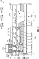
- FIG. 2 illustrates a partial cross-sectional view of an electronic device (e.g., a display device) 10 of embodiments of the present disclosure.
- the electronic device 10 may include a composite substrate 100, as shown in FIG. 2 .
- the composite substrate 100 may include a transparent substrate, but the present disclosure is not limited thereto.
- the composite substrate 100 may include a sub-layer 102, a substrate 104, and thin-film transistors disposed on the substrate 104.
- the thin-film transistors may include an active layer 110, a gate insulating layer 112 and a gate layer 114 which will be discussed in the following paragraphs.
- the composite substrate 100 may include the substrate 104 and the thin-film transistors disposed on the substrate 104, but not include the sub-layer 102.
- the substrate 104 may include a non-bending portion 104a and a bendable (or flexible) portion 104b.
- the bendable portion 104b is adjacent to the non-bending portion 104a.
- the bendable portion 104b of the substrate 104, and the layers and elements formed on the bendable portion 104b of the electronic device 10 may be bent.
- thin-film transistors may be disposed on and/or in the non-bending portion 104a of the substrate 104, and conductive lines may be disposed on and/or in the bendable portion 104b of the substrate 104.
- the present disclosure is not limited thereto.
- the substrate 104 is a flexible layer. In some embodiments, the ductility of the substrate 104 is greater than that of the sub-layer 102. In some embodiments, the strength (e.g., the tensile strength) of the sub-layer 102 is greater than that of the substrate 104.
- the sub-layer 102 and the substrate 104 include different materials.
- the sub-layer 102 may include glass, and the substrate 104 may include polyimide or polyethylene terephthalate, but the present disclosure is not limited thereto.
- the sub-layer 102 and the substrate 104 may include any other applicable materials.
- the substrate 104 may be formed on the sub-layer 102 by using a spin-on coating process, a rolling process, a vacuum laminating process, a chemical vapor deposition process, another applicable process, or a combination thereof, but the present disclosure is not limited thereto.
- one or more openings (or recesses) 102a may be formed under the bendable portion 104b of the substrate 104. Therefore, the problem of cracking due to the low ductility of the sub-layer 102 may be alleviated when the composite substrate 100 is bent.
- the opening (or recess) 102a may expose the substrate 104 of the composite substrate 100, but the present disclosure is not limited thereto. In some other embodiments, the opening (or recess) 102a may not expose the substrate 104 of the composite substrate 100.
- the electronic device 10 may include an insulating layer 106 disposed on the substrate 104.
- the insulating layer 106 may block the moisture and the oxygen to reduce the oxidation of the layers disposed on the insulating layer 106.
- the insulating layer 106 may include silicon nitride, silicon oxide, aluminum oxide, another applicable material, or a combination thereof, and the insulating layer 106 may be formed by using a chemical vapor deposition process, a thermal oxidation process, another applicable process, or a combination thereof, but the present disclosure is not limited thereto.
- a patterning process may be performed on the insulating layer 106 to form a portion of an opening O 1 in the insulating layer 106.
- the opening O 1 may be located on and/or in the bendable portion 104b of the substrate 104.
- the opening O 1 may expose the top surface of the substrate 104.
- the opening O 1 in the top view, may be substantially oval, square, rectangular, round, oblong, triangular, polygonal, irregular shape, another applicable shape, or a combination thereof.
- the patterning process may include a lithography process, an etching process, another applicable process, or a combination thereof.
- the lithography process may include photoresist coating (e.g., spin-on coating), soft baking, mask aligning, exposure, post-exposure, developing photoresist, rising, drying (e.g., hard baking), another applicable process, or a combination thereof.
- the etching process may include a dry etching process (e.g., a plasma etching process), a wet etching process, another applicable process, or a combination thereof.
- the electronic device 10 may include an insulating layer 108 disposed on the insulating layer 106.
- the insulating layer 108 may include silicon nitride, silicon oxide, aluminum oxide, another applicable material, or a combination thereof, and the insulating layer 108 may be formed by using a chemical vapor deposition process, a thermal oxidation process, another applicable process, or a combination thereof, but the present disclosure is not limited thereto.
- the insulating layer 106 and the insulating layer 108 may include the same material, but the present disclosure is not limited thereto.
- the insulating layer 106 and the insulating layer 108 may include different materials (e.g., the insulating layer 106 includes silicon oxide and the insulating layer 108 includes silicon nitride).
- a patterning process may be performed on the insulating layer 108 to form a portion of the opening O 1 in the insulating layer 108.
- the portion of the opening O 1 in the insulating layer 108 is in communication with the portion of the opening O 1 in the insulating layer 106.
- the patterning process may include a lithography process, an etching process, another applicable process, or a combination thereof.
- the electronic device 10 may include an active layer 110 disposed on the insulating layer 108.
- the active layer 110 may include poly-silicon, and the poly-silicon may be formed by using a low temperature poly-silicon (LTPS) process, but the present disclosure is not limited thereto.
- the active layer 110 may include amorphous silicon (a-Si), indium gallium zinc oxide (IGZO), other applicable materials, or a combination thereof.
- the active layer 110 may include source/drain regions 110a and a channel region 110b of a thin-film transistor.
- the source/drain regions 110a are the source/drain regions of a n-type thin-film transistor, and therefore the source/drain regions 110a may be doped with phosphorus, arsenic, antimony, another applicable n-type dopant, or a combination thereof.
- the source/drain regions 110a are the source/drain regions of a p-type thin-film transistor, and therefore the source/drain regions 110a may be doped with boron, indium, another applicable p-type dopant, or a combination thereof.
- an ion implantation process may be used to implant appropriate dopants into the active layer 110 so as to form the source/drain regions 110a of the thin-film transistor.
- the electronic device 10 may include a gate insulating layer 112 disposed on the active layer 110.
- the gate insulating layer 112 may include silicon oxide, silicon nitride, silicon oxynitride, other applicable materials, or a combination thereof.
- the gate insulating layer 112 may include a high-k dielectric material (e.g., LaO, AlO, ZrO, TiO, Ta 2 O 5 , Y 2 O 3 , SrTiO 3 (STO) , BaTiO 3 (BTO), BaZrO, HfO 2 , HfO 3 , HfZrO, HfLaO, HfSiO, HfSiON, LaSiO, AlSiO, HfTaO, HfTiO, HfTaTiO, HfAlON, (Ba,Sr) TiO 3 (BST), Al 2 O 3 , another applicable material, or a combination thereof).
- a high-k dielectric material e.g., LaO, AlO, ZrO, TiO, Ta 2 O 5 , Y 2 O 3 , SrTiO 3 (STO) , BaTiO 3 (BTO), BaZrO, HfO 2 , HfO
- the gate insulating layer 112 may be formed by using a chemical vapor deposition process, a spin-on coating process, an atomic layer deposition process, another applicable process, or a combination thereof.
- a chemical vapor deposition process may include a low pressure chemical vapor deposition (LPCVD) process, a low temperature chemical vapor deposition (LTCVD) process, a rapid thermal chemical vapor deposition (RTCVD) process, a plasma enhanced chemical vapor deposition (PECVD) process, another applicable chemical vapor deposition process, or a combination thereof.
- LPCVD low pressure chemical vapor deposition
- LTCVD low temperature chemical vapor deposition
- RTCVD rapid thermal chemical vapor deposition
- PECVD plasma enhanced chemical vapor deposition
- a patterning process may be performed on the gate insulating layer 112 to form a portion of the opening O 1 in the gate insulating layer 112.
- the portion of the opening O 1 in the gate insulating layer 112 is in communication with the portion of the opening O 1 in the insulating layer 108.
- the patterning process may include a lithography process, an etching process, another applicable process, or a combination thereof.
- the electronic device 10 may include a gate layer 114 disposed on the gate insulating layer 112.
- the active layer 110, the gate insulating layer 112 and the gate layer 114 can be together to form a thin-film transistor.
- the current signal transmitted to the light-emitting unit (e.g., light-emitting unit 150 which will be discussed in the following paragraphs) of the electronic device 10 can be controlled through the thin-film transistor discussed above, such that the light-emitting performance of the light-emitting unit of the electronic device 10 can be controlled.
- the gate layer 114 may include or electrically connect to the scan lines of the electronic device 10.
- the gate layer 114 may include a metal, a metal nitride, a metal oxide, another applicable conductive material, or a combination thereof.
- the metal may include copper, molybdenum, tungsten, titanium, tantalum, platinum, hafnium, another applicable metal, or a combination thereof.
- the metal nitride may include molybdenum nitride, tungsten nitride, titanium nitride, tantalum nitride, another applicable metal nitride, or a combination thereof.
- the metal oxide may include ruthenium oxide, indium tin oxide, another applicable metal oxide, or a combination thereof.
- the gate layer 114 may be formed by using a chemical vapor deposition process, a physical vapor deposition process (e.g., a sputtering process or an evaporation process), another applicable process, or a combination thereof, but the present disclosure is not limited thereto.
- the electronic device 10 may include an insulating layer 116 disposed on the gate layer 114.
- the insulating layer 116 may serve as the insulating layer of a metal-insulator-metal (MIM) capacitor structure.
- the insulating layer 116 may include silicon nitride, silicon oxide, aluminum oxide, another applicable material, or a combination thereof, and may be formed by using a chemical vapor deposition process, a thermal oxidation process, another applicable process, or a combination thereof, but the present disclosure is not limited thereto.
- a patterning process may be performed on the insulating layer 116 to form a portion of the opening O 1 in the insulating layer 116.
- the portion of the opening O 1 in the insulating layer 116 is in communication with the portion of the opening O 1 in the gate insulating layer 112.
- the patterning process may include a lithography process, an etching process, another applicable process, or a combination thereof.
- the electronic device 10 may include a metal layer 118 disposed on the insulating layer 116.
- the gate layer 114, the insulating layer 116 and the metal layer 118 may be together to form a metal-insulator-metal capacitor structure.
- the materials and forming methods of the metal layer 118 may be the same as or similar to those of the gate layer 114. In the interest of simplicity and clarity, the details will not be discussed again.
- the electronic device 10 may include a dielectric layer 120 disposed on the insulating layer 116 and the metal layer 118.
- the dielectric layer 120 may include silicon oxide, silicon nitride, another applicable material, or a combination thereof, and may be formed by using a chemical vapor deposition process, a thermal oxidation process, another applicable process, or a combination thereof, but the present disclosure is not limited thereto.
- a patterning process may be performed on the dielectric layer 120 to form a portion of the opening O 1 in the dielectric layer 120.
- the portion of the opening O 1 in the dielectric layer 120 is in communication with the portion of the opening O 1 in the insulating layer 116.
- the patterning process may include a lithography process, an etching process, another applicable process, or a combination thereof.
- the electronic device 10 may include a conductive layer 124 disposed on the dielectric layer 120.
- the conductive layer 124 may include or electrically connect to the data lines of the electronic device 10.
- the electronic device 10 may include one or more conductive vias penetrating the dielectric layer 120, the insulating layer 116 and/or the gate insulating layer 112, and the conductive layer 124 may be electrically connected to the active layer 110 through the conductive via(s).
- the conductive layer 124 may be in direct contact with the source/drain regions 110a of the active layer 110.
- the metal layer 118 may be electrically connected to the active layer 110 through the conductive layer 124.
- the conductive layer 124 may include copper, molybdenum, tungsten, titanium, aluminum, tantalum, platinum, hafnium, another applicable conductive material, or alloys thereof.
- a patterning process (e.g., a lithography process, an etching process, another applicable process, or a combination thereof) may be utilized to form one or more appropriate openings in the dielectric layer 120, the insulating layer 116 and/or the gate insulating layer 112, and then the one or more openings may be filled with a conductive material to form the conductive layer 124 in the one or more openings by using a physical vapor deposition process (e.g., a sputtering process or an evaporation process), an electroplating process, another applicable process, or a combination thereof.
- a physical vapor deposition process e.g., a sputtering process or an evaporation process
- electroplating process another applicable process, or a combination thereof.
- a physical vapor deposition process e.g., a sputtering process or an evaporation process
- an electroplating process another applicable process, or a combination thereof
- a patterning process e.g., a lithography process, an etching process, another applicable process, or a combination thereof
- the electronic device 10 may include a passivation layer 126 disposed on the conductive layer 124 and the dielectric layer 120.
- the passivation layer 126 may include silicon nitride, silicon oxide, aluminum oxide, other applicable materials, or a combination thereof, and the passivation layer 126 may be formed by using a chemical vapor deposition process, a thermal oxidation process, another applicable process, or a combination thereof, but the present disclosure is not limited thereto.
- a patterning process may be performed on the passivation layer 126 to form a portion of the opening O 1 in the passivation layer 126.
- the portion of the opening O 1 in the passivation layer 126 is in communication with the portion of the opening O 1 in the dielectric layer 120.
- the patterning process may include a lithography process, an etching process, another applicable process, or a combination thereof.
- the electronic device 10 may include one or more bridging elements 128 disposed on the passivation layer 126 and penetrating the passivation layer 126.
- the bridging element 128 and the conductive layer 124 may include different materials, but the present disclosure is not limited thereto.
- the bridging element 128 may include indium tin oxide (ITO), tin oxide (SnO), indium zinc oxide (IZO), indium gallium zinc oxide (IGZO), indium tin zinc oxide (ITZO), antimony tin oxide (ATO), antimony zinc oxide (AZO), another applicable transparent conductive material, or a combination thereof.
- the bridging element 128 may include copper, molybdenum, tungsten, titanium, aluminum, tantalum, platinum, hafnium, another applicable metal, or a combination thereof, but the present disclosure is not limited thereto.
- a patterning process (e.g., a lithography process, an etching process, another applicable process, or a combination thereof) may be utilized to form one or more appropriate openings in the passivation layer 126, and then a physical vapor deposition process (e.g., a sputtering process or an evaporation process), an atomic layer deposition process, another applicable process, or a combination thereof may be utilized to fill the one or more openings with an appropriate conductive material and to form a conductive blanket layer on the passivation layer 126, and then a patterning process (e.g., a lithography process, an etching process, another applicable process, or a combination thereof) may be performed on the conductive blanket layer to form the bridging element 128.
- a physical vapor deposition process e.g., a sputtering process or an evaporation process
- an atomic layer deposition process e.g., another applicable process, or a combination thereof
- the electronic device 10 may include an insulating layer 130 disposed on the passivation layer 126 and the bendable portion 104b.
- the insulating layer 130 may fill the opening O 1 .
- the ductility of the insulating layer 130 including an organic photoresist material is better than the ductility of the insulating layer 106, the insulting layer 108, the gate insulating layer 112, the insulating layer 116, the dielectric layer 120 and/or the passivation layer 126.
- the opening O 1 is filled with the insulating layer 130 (i.e., a portion of the insulating layer 106, a portion of the insulting layer 108, a portion of the gate insulating layer 112, a portion of the insulating layer 116, a portion of the dielectric layer 120 and/or a portion of the passivation layer 126 is replaced with a portion of the insulating layer 130) having better ductility, the occurrence of cracking when bending the electronic device 10 can be reduced.
- the insulating layer 130 i.e., a portion of the insulating layer 106, a portion of the insulting layer 108, a portion of the gate insulating layer 112, a portion of the insulating layer 116, a portion of the dielectric layer 120 and/or a portion of the passivation layer 126 is replaced with a portion of the insulating layer 130
- an organic photoresist material with good fluidity may be coated on the non-bending portion 104a and the bendable portion 104b of the substrate 104 by a spin-on coating process or a slit coating process, then an applicable patterning process (e.g., a lithography process, an etching process, another applicable process, or a combination thereof) may be performed to form the insulating layer 130.
- an applicable patterning process e.g., a lithography process, an etching process, another applicable process, or a combination thereof
- the organic photoresist material used for forming the insulating layer 130 since the organic photoresist material used for forming the insulating layer 130 has good fluidity, it can compensate the height difference of the surfaces of the structure of the layers discussed above to planarize the surface of the structure. Accordingly, the insulating layer 130 may have a substantially planar top surface. In some embodiments, the top surface of the insulating layer 130 may be substantially parallel to the top surface of the substrate 104, but the
- the insulating layer 130 on the non-bending portion 104a of the substrate 104 may have a thickness T 1
- the insulating layer 130 on the bendable portion 104b of the substrate 104 may have a thickness T 2 .
- the thickness T 1 is less than the thickness T 2 , but the present disclosure is not limited thereto.
- the electronic device 10 may include a conductive layer 134 disposed on the insulating layer 130.
- the conductive layer 134 may include conductive lines, conductive pads, other applicable conductive elements, or a combination thereof.
- the electronic device 10 may include one or more conductive vias disposed in the insulating layer 130, and the conductive layer 134 may be electrically connected to the bridging element(s) 128 through the conductive via(s). In some embodiments, the conductive layer 134 is electrically connected to the conductive layer 124 through the bridging element(s) 128.
- the conductive layer 134 may include molybdenum, tungsten, titanium, aluminum, tantalum, platinum, hafnium, copper, another applicable conductive material, or a combination thereof. In some embodiments, the conductive layer 134 may include a stacking structure containing multiple metal layers (e.g., Ti/Al/Ti stacking structure).
- one or more appropriate openings may be formed in the insulating layer 130 by a lithography process, and then a physical vapor deposition process (e.g., a sputtering process or an evaporation process), an electroplating process, another applicable process, or a combination thereof may be used to fill the opening(s) with a conductive material so as to form the conductive layer 134 in the opening(s).
- a physical vapor deposition process e.g., a sputtering process or an evaporation process
- an electroplating process e.g., a conductive material
- another applicable process e.g., a conductive material
- the bridging elements 128 include the transparent conductive material (e.g., ITO) discussed above, since the transparent conductive material is less susceptible to damage by the developer, the bridging elements 128 can reduce the occurrence of the underlying layers (e.g., the conductive layer 124) being damaged by the developer.
- the transparent conductive material e.g., ITO
- a physical vapor deposition process e.g., a sputtering process or an evaporation process
- an electroplating process another applicable process, or a combination thereof
- a patterning process e.g., a lithography process, an etching process, another applicable process, or a combination thereof
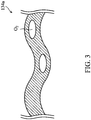
- the conductive layer 134 includes a conductive line 134a and one or more openings O 2 on the bendable portion 104b.
- the opening(s) O 2 may be formed in the conductive line 134a of the conductive layer 134, as shown in FIG. 3 .
- the conductive line 134a has an undulating or wavy edge.
- at least one of the openings O 2 may fully overlap or partially overlap the opening O 1 .
- the conductive line 134a since the conductive line 134a has the undulating edge and/or the opening(s) O 2 , the occurrence of the conductive layer 134 cracking when bending the electronic device 10 can be reduced.
- the opening(s) O 2 may be formed in the conductive layer 134 by using a patterning process (e.g., a lithography process, an etching process, another applicable process, or a combination thereof).
- a patterning process e.g., a lithography process, an etching process, another applicable process, or a combination thereof.
- the opening(s) O 2 in the top view, may be substantially oval, square, rectangular, round, oblong, triangular, polygonal, irregular shape, another applicable shape, or a combination thereof.
- the electronic device 10 may include an insulating layer 136 disposed on the conductive layer 134 and the insulating layer 130.
- the opening(s) O 2 may be filled by the insulating layer 136.
- the materials and forming methods of the insulating layer 136 may be the same as or similar to those of the insulating layer 130. In the interest of simplicity and clarity, the details will not be discussed again.
- the top surface of the insulating layer 136 can be substantially planar. In some embodiments, the top surface of the insulating layer 136 may be substantially parallel to the top surface of the substrate 104, but the present disclosure is not limited thereto.
- the insulating layer 136 may have a thickness T 3 .
- the thickness T 3 may be in a range from about 1 ⁇ m to about 5 ⁇ m, but the present disclosure is not limited thereto.
- the electronic device 10 may include an insulating layer 138.
- the insulating layer 138 may extend from the top surface of the insulating layer 136 into the insulating layer 136.
- the insulating layer 138 may include silicon nitride, another applicable insulating material, or a combination thereof.
- the insulating layer 138 and the insulating layer 136 may include different materials.
- the thickness of the insulating layer 138 may be in a range from about 0.1 ⁇ m to about 1 ⁇ m, but the present disclosure is not limited thereto.
- one or more appropriate openings may be formed in the insulating layer 136 by a lithography process, and then the insulating layer 138 may be formed by depositing an insulating material in the opening(s) and on the top surface of the insulating layer 136 by using a chemical vapor deposition process, another applicable process, or a combination thereof.
- a patterning process may be performed on the insulating layer 138 to form a portion of an opening O 3 in the insulating layer 138.
- the opening O 3 may be located on the bendable portion 104b.
- the opening O 3 in the top view, may fully overlap or partially overlap the opening O 1 .
- the opening O 3 in the top view, may fully overlap or partially overlap at least one of the openings O 2 .
- the opening O 3 in the top view, may be substantially oval, square, rectangular, round, oblong, triangular, polygonal, irregular shape, another applicable shape, or a combination thereof.
- the patterning process may include a lithography process, an etching process, another applicable process, or a combination thereof.
- the electronic device 10 may include a conductive layer 142 disposed on the insulating layer 136.
- the conductive layer 142 may include conductive lines, conductive pads, other applicable conductive elements, or a combination thereof.
- the conductive layer 142 is electrically connected to the conductive layer 134 through the conductive vias.
- the conductive layer 142 may include molybdenum, tungsten, titanium, aluminum, tantalum, platinum, hafnium, copper, chromium, lead, nickel, zinc, indium, gold, alloys thereof, other applicable conductive materials, or a combination thereof.
- the conductive layer 142 may include a stacking structure containing multiple metal layers (e.g., Mo/Cu stacking structure).
- the thickness of the conductive layer 142 may be in a range from about 0.5 ⁇ m to about 5 ⁇ m, but the present disclosure is not limited thereto.
- one or more appropriate openings may be formed in the insulating layer 136 by a lithography process, and then a physical vapor deposition process (e.g., a sputtering process or an evaporation process), an electroplating process, another applicable process, or a combination thereof may be used to fill the opening(s) with a conductive material so as to form the conductive layer 142 in the opening(s).
- a physical vapor deposition process e.g., a sputtering process or an evaporation process
- an electroplating process e.g., a conductive material
- a physical vapor deposition process e.g., a sputtering process or an evaporation process
- an electroplating process another applicable process, or a combination thereof
- a patterning process e.g., a lithography process, an etching process, another applicable process, or a combination thereof
- the insulating layer 138 disposed between the conductive layer 142 and the insulating layer 136 may serve as an adhesive layer, to reduce peeling of the conductive layer 142 from the insulating layer 136.
- the electronic device 10 may include an insulating layer 144 disposed on the insulating layer 138 and the conductive layer 142.
- the top surface of the insulating layer 144 may be substantially planar.
- the top surface of the insulating layer 144 may be substantially parallel to the top surface of the substrate 104, but the present disclosure is not limited thereto.
- the conductive pads e.g., conductive pads 146a and 146b which will be discussed in the following paragraphs
- the conductive pads used for connecting the light-emitting unit may be located at substantially the same level. Therefore, the problem of poor bonding between the light-emitting unit and the conductive pads can be alleviated, and thus the yield of the electronic device can be improved.
- the insulating layer 144 may include silicon nitride, silicon oxide, another applicable material, or a combination thereof. In some embodiments, the insulating layer 144 may include a polymer material. In some embodiments, the insulating layer 144 may include an organic photoresist material.
- the insulating layer 144 may be formed by using a chemical vapor deposition process, a thermal oxidation process, another applicable process, or a combination thereof.
- the process for forming the insulating layer 144 may include a spin-on coating process, a curing process, another applicable process, or a combination thereof.
- a patterning process may be performed on the insulating layer 144 to form a portion of the opening O 3 in the insulating layer 144.
- the portion of the opening O 3 in the insulating layer 144 is in communication with the portion of the opening O 3 in the insulating layer 138.
- the patterning process may include a lithography process, an etching process, another applicable process, or a combination thereof.
- the electronic device 10 may include a conductive pad 146a and a conductive pad 146b.
- at least a portion of the insulating layer 144 is located between the conductive pads (e.g., the conductive pad 146a and the conductive pad 146b).
- the conductive pad 146a and the conductive pad 146b may be located at substantially the same level, thus reducing the problem of the poor bonding between the light-emitting unit (e.g., light-emitting unit 150 which will be discussed in the following paragraphs) and the conductive pads (e.g., conductive pads 146a and 146b) and improving the yield of the electronic device.
- the top surface of the conductive pad 146a and the top surface of the conductive pad 146b may be located at substantially the same level. In some embodiments, the top surface of the conductive pad 146a and the top surface of the conductive pad 146b may be coplanar.
- the conductive pad 146a and the conductive pad 146b may extend from the top surface of the insulating layer 144 into the insulating layer 144.
- the conductive pad 146a and the conductive pad 146b may include molybdenum, tungsten, titanium, aluminum, tantalum, platinum, hafnium, copper, chromium, lead, nickel, zinc, indium, gold, alloys thereof, other applicable conductive materials, or a combination thereof.
- the conductive pad 146a and the conductive pad 146b may include a stacking structure containing multiple metal layers (e.g., a Ni/Au stacking structure).
- the outermost layer of the conductive pad 146a and the conductive pad 146b may be an antioxidation layer including a metal with good oxidation resistance (e.g., Pt, Au, Pd, or a combination thereof), but the present disclosure is not limited thereto.
- a metal with good oxidation resistance e.g., Pt, Au, Pd, or a combination thereof
- a patterning process (e.g., a lithography process, an etching process, another applicable process, or a combination thereof) may be performed to form appropriate openings in the insulating layer 144, then a physical vapor deposition process, an electroplating process, an electroless plating process, another applicable process, or a combination thereof may be applied to deposit a conductive material in the openings and on the top surface of the insulating layer 144 to form the conductive pad 146a and the conductive pad 146b.
- a patterning process e.g., a lithography process, an etching process, another applicable process, or a combination thereof
- the electronic device 10 may include a light-emitting unit 150 connected to the conductive pad 146a and the conductive pad 146b.
- the light-emitting unit 150 may include a light-emitting diode (e.g., a blue light-emitting diode, a red light-emitting diode, or a green light-emitting diode), an organic light-emitting diode, a micro light-emitting diode, a quantum-dot light-emitting diode, a mini light-emitting diode, another applicable light-emitting unit, or a combination thereof.
- a light-emitting diode e.g., a blue light-emitting diode, a red light-emitting diode, or a green light-emitting diode
- an organic light-emitting diode e.g., a micro light-emitting diode, a quantum-do
- the light-emitting unit 150 may be electrically connected to the source/drain regions 110a of the active layer 110 through the conductive pads 146a and 146b, the conductive layer 142, the conductive layer 134, and the conductive layer 124.
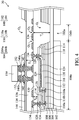
- FIG. 4 illustrates an electronic device (e.g., a display device) 20 according to some embodiments of the present disclosure.
- the light-emitting unit 150 and the active layer 110 of the electronic device 20 are laterally spaced apart from each other.
- the active layer 110 and the light emitting unit 150 do not overlap in the normal direction, and the normal direction may refer to a direction that is perpendicular to the top surface of the substrate 104 in the present disclosure.
- the light-emitting unit 150 and the active layer 110 of the electronic device 20 are laterally spaced apart from each other, occurrences of the active layer 110 being crushed by the light-emitting unit 150 when bonding the light-emitting unit 150 to the conductive pads 146a and 146b can be reduced.
- the light-emitting unit 150 may include a main portion (e.g., light-emitting chip(s) C1 which will be discussed in the following paragraphs) and a connection feature.
- the main portion of the light-emitting unit 150 may include gallium nitride, aluminum gallium nitride, aluminum nitride, gallium arsenide, indium gallium phosphide, aluminum gallium arsenide, indium phosphide, indium aluminum arsenide, indium gallium arsenide, aluminum gallium indium phosphide, another applicable semiconductor material, or a combination thereof, but the present disclosure is not limited thereto.
- the light-emitting unit 150 may be electrically connected to the conductive pads 146a and 146b through its connection feature. In other words, the light-emitting unit 150 may be electrically connected to the thin-film transistor through its connection feature.
- the connection feature of the light-emitting unit 150 may include conductive wiring layers, conductive pads, electrodes, bumps, other applicable connection features, or a combination thereof.
- connection feature of the light-emitting unit 150 may include a metal (e.g., copper, tungsten, silver, tin, nickel, chromium, titanium, lead, gold, bismuth, antimony, zinc, zirconium, magnesium, indium, tellurium, gallium, or another applicable metal), an alloy thereof, another applicable conductive material, or a combination thereof, but the present disclosure is not limited thereto.
- a metal e.g., copper, tungsten, silver, tin, nickel, chromium, titanium, lead, gold, bismuth, antimony, zinc, zirconium, magnesium, indium, tellurium, gallium, or another applicable metal
- an alloy thereof e.g., copper, tungsten, silver, tin, nickel, chromium, titanium, lead, gold, bismuth, antimony, zinc, zirconium, magnesium, indium, tellurium, gallium, or another applicable metal
- the light-emitting unit 150 may be electrically connected to the conductive pads 146a and 146b through a conductive medium 152.
- the conductive medium 152 overlaps the conductive pads 146a and 146b in the normal direction.
- the conductive medium 152 is in direct contact with the conductive pads 146a and 146b and with the connection feature of the light-emitting unit 150.
- the conductive medium 152 may include tin, tin alloy, conductive glue (e.g., anisotropic conductive film), another applicable material, or a combination thereof.
- the process for bonding the light-emitting unit 150 to the conductive pad 146a and the conductive pad 146b may include a soldering process, but the present disclosure is not limited thereto.
- a eutectic bonding process may be performed to cause a eutectic reaction between the connection feature of the light-emitting unit 150 and the conductive pad (e.g., the conductive pads 146a and 146b), so as to bond the light-emitting unit 150 to the conductive pad (e.g., the conductive pads 146a and 146b).
- FIG. 5 illustrates a cross-sectional view of the light-emitting unit 150 according to some embodiments of the present disclosure.
- the light-emitting unit 150 may include a packaging substrate 202, the packaging substrate 202 may be a flat plate, and conductive wiring layers 204 and 206 may be disposed on the surfaces of the packaging substrate 202 and in the packaging substrate 202.
- the light-emitting unit 150 has a light-emitting chip (e.g., a light-emitting diode chip) C1, the light-emitting chip C1 is disposed on the packaging substrate 202 with its conductive end facing downward, and the light-emitting chip C1 may be electrically connected to the conductive wiring layers 204 and 206 of the surfaces of the packaging substrate 202 through bonding pads 210 or another applicable material such as solder balls. In some embodiments, the light-emitting unit 150 may be electrically connected to the conductive pads 146a and 146b directly through the conductive wiring layers 204 and 206 thereof.
- a light-emitting chip e.g., a light-emitting diode chip
- the light-emitting unit 150 may further include conductive pads 150a and 150b disposed under the conductive wiring layers 204 and 206, and the light-emitting unit 150 may be electrically connected to the conductive pads 146a and 146b through the conductive wiring layers 204 and 206 and the conductive pads 150a and 150b.
- Each or the whole of the conductive wiring layer 204, the conductive wiring layer 206, the bonding pads 210, the conductive pad 150a, and the conductive pad 150b may be considered as the connection feature of the light-emitting unit 150.
- the packaging substrate 202 including the conductive wiring layers 204 and 206 may serve as a support structure for supporting the light-emitting chip C1.
- the light-emitting unit 150 of the embodiments illustrated in FIG. 5 has only one light-emitting chip C1, the present disclosure is not limited thereto.
- the light-emitting unit 150 may include a plurality of light-emitting chips.
- the light-emitting unit 150 may have a light-emitting chip C1, a light-emitting chip C2, and a light-emitting chip C3.
- the light-emitting chip C1, the light-emitting chip C2, and the light-emitting chip C3 may respectively emit a red light, a green light, and a blue light.
- the light-emitting unit 150 may also include encapsulating glue 208, and the encapsulating glue 208 may be disposed on the light-emitting chip (e.g., the light-emitting chip C1, the light-emitting chip C2, and the light-emitting chip C3) and the packaging substrate 202.
- the encapsulating glue 208 may be disposed on the light-emitting side of the light-emitting chip.
- the material of the encapsulating glue 208 may be epoxy based resin or silicone, but the present disclosure is not limited thereto.
- a plurality of light-emitting units 150 are disposed on the composite substrate 100 of the electronic device 10.
- the plurality of light-emitting units 150 on the composite substrate 100 are separate from each other, and thus the packaging substrate 202 and the encapsulating glue 208 of a first light-emitting unit 150 are not in direct contact with the packaging substrate 202 and the encapsulating glue 208 of a second light-emitting unit 150 adjacent to the first light-emitting unit 150.
- respective encapsulating glue may be disposed respectively on light-emitting chip C1, C2 or C3.
- FIGS. 7 to 10 illustrate some variant embodiments of the light-emitting unit 150 of the present disclosure.
- the elements and layers the same as or similar to those discussed in the above embodiments will be denoted by the same reference numerals, and the materials and forming methods thereof may also be the same as or similar to those discussed in the above embodiments.
- the number of light-emitting chips packaged in the light-emitting unit 150 is not limited thereto. Further, the light-emitting unit 150 may have any suitable number of light-emitting chips packaged by the encapsulating glue 208 according to the design requirement.
- FIG. 7 illustrates a variant embodiment of the light-emitting unit 150 of the present disclosure.
- the light-emitting chip C1 of the light-emitting unit 150 of the embodiment illustrated in FIG. 7 is disposed on the surface of the packaging substrate 202 with its conductive end facing upward.
- the conductive end (not shown in the figures) of the surface of the light-emitting chip C1 may be electrically connected to the conductive wiring layer 204 and the conductive wiring layer 206 of the surfaces of the packaging substrate 202 through conductive wires 214.
- each or the whole of the conductive wiring layer 204, the conductive wiring layer 206, and the conductive wires 214 may be considered as the connection feature of the light-emitting unit 150.
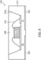
- FIG. 8 illustrates a variant embodiment of the light-emitting unit 150 of the present disclosure.
- a packaging substrate 212 has a sidewall 212a and thus forms a cup-shaped structure surrounding the light-emitting chip C1.
- the light-emitting chip C1 may be disposed in the chamber or recess of the packaging substrate 212, and the light-emitting chip C1 may be electrically connected to the conductive wiring layers 204 and 206 disposed in the packaging substrate 212 through the conductive wires 214.
- the encapsulating glue 208 may be disposed in the chamber or recess of the packaging substrate 212 to overlie and protect the light-emitting chip C1.
- the packaging substrate of the embodiments illustrated in FIG. 7 and FIG. 8 may have high reflectivity to improve the light utilization efficiency.
- the packaging substrate 212 including the conductive wiring layers 204 and 206 may serve as a support structure for supporting the light-emitting chip C1.
- each or the whole of the conductive wiring layer 204, the conductive wiring layer 206, and the conductive wires 214 may be considered as the connection feature of the light-emitting unit 150.
- FIG. 9 illustrates a variant embodiment of the light-emitting unit 150 of the present disclosure.
- the light-emitting chip C1 is packaged with its conductive end facing downward, and the encapsulating glue 208 is disposed on the light-emitting chip C1 to form the light-emitting unit 150.
- the bonding pads 210 are exposed by the encapsulating glue 208, and thus the light-emitting chip C1 can be electrically connected to the conductive pads 146a and 146b directly through the bonding pads 210 without using the cup-shaped support or the packaging substrate 202 of the above embodiments.
- the bonding pads 210 are in direct contact with the conductive pads 146a and 146b.
- each or all of the bonding pads 210 can be considered as the connection feature of the light-emitting unit 150.
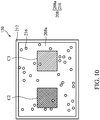
- FIG. 10 illustrates a top plan view showing a variant embodiment of the light-emitting unit 150 of the present disclosure.
- the light-emitting unit 150 includes two light-emitting chips C2 and C3.
- the color of the light emitted by the light-emitting chip C2 is different from the color of the light emitted by the light-emitting chip C3.
- the light-emitting chip C2 may emit blue light
- the light-emitting chip C3 may emit green light.
- the encapsulating glue 208 of the light-emitting unit 150 may include an encapsulating material (e.g., epoxy based resin or silicone) 208a and phosphor powders (e.g., red phosphor powders) 216 dispersed in the encapsulating material 208a.
- an encapsulating material e.g., epoxy based resin or silicone
- phosphor powders e.g., red phosphor powders
- part of the blue light and/or the green light may be converted into red light, and thus the light-emitting unit 150 can generate white light by mixing the green light, the blue light, and the red light.
- the light-emitting unit 150 of the present disclosure only has a blue light-emitting chip, and the encapsulating glue 208 includes yellow phosphor powders therein, and thus the light-emitting unit 150 can generate white light.
- the light-emitting unit 150 of the present disclosure only has a blue light-emitting chip, and the encapsulating glue 208 includes quantum dots with different diameters, and thus the light-emitting unit 150 can generate lights of different colors.
- quantum dots may be disposed on the light-emitting chip of the light-emitting unit 150 of the present disclosure.
- the encapsulating glue 208 of the light-emitting unit 150 of the present disclosure may include light-diffusing particles therein to improve the brightness uniformity when emitting the light.
- the light-emitting units 150 with different encapsulating glues discussed above, or other applicable light-emitting units, may be applied in the embodiments and variant embodiments of the present disclosure. Further details will not be discussed herein.
- the cover plate may include glass, indium tin oxide, polyimide, polyethylene terephthalate, another applicable material, or a combination thereof, but the present disclosure is not limited thereto.
- the optical film may include a diffuser film, a condenser lens, another applicable optical film, or a combination thereof, but the present disclosure is not limited thereto.
- the electronic device 10 can include any suitable number of light-emitting units 150.
- these light-emitting units 150 have corresponding encapsulating glues 208, and some of the corresponding encapsulating glues 208 are separated from each other.
- these light-emitting units 150 have corresponding packaging substrates 202, and some of the corresponding packaging substrates 202 are separated from each other, but the encapsulating glues 208 are connected to each other.
- the electronic device 10 e.g., a display device
- a curved electronic device e.g., a curved display device
- the curved electronic devices in these embodiments may include technical features the same as or similar to those of the electronic device 10, and they should be included in the scope of the present disclosure.
- an electronic device e.g., a display device
- a big size may be formed by assembling a plurality of the electronic devices (e.g., a display device) 10 in some embodiments, and it should be included in the scope of the present disclosure.
- composite substrate 100 and the layers and elements on the composite substrate 100 of the electronic device 10 may serve as a back light unit or back light module.
- an insulating layer with a good ductility may be disposed on the substrate of the electronic device of the present disclosure, thus reducing the occurrence of cracking when bending the electronic device.
- a substantially planar insulating layer may be disposed between the light-emitting unit and the substrate of the electronic device, so that the conductive pads used for connecting the light-emitting unit can be located at substantially the same level, thus reducing the occurrence of the poor bonding between the light-emitting unit and the conductive pads and improving the yield of the electronic device.
Landscapes
- Electroluminescent Light Sources (AREA)
- Thin Film Transistor (AREA)
- Led Device Packages (AREA)
Applications Claiming Priority (2)
| Application Number | Priority Date | Filing Date | Title |
|---|---|---|---|
| US201862659794P | 2018-04-19 | 2018-04-19 | |
| CN201811178409.7A CN110391252A (zh) | 2018-04-19 | 2018-10-10 | 电子装置 |
Publications (3)
| Publication Number | Publication Date |
|---|---|
| EP3557618A2 true EP3557618A2 (fr) | 2019-10-23 |
| EP3557618A3 EP3557618A3 (fr) | 2020-01-15 |
| EP3557618B1 EP3557618B1 (fr) | 2022-10-26 |
Family
ID=66175323
Family Applications (1)
| Application Number | Title | Priority Date | Filing Date |
|---|---|---|---|
| EP19169096.5A Active EP3557618B1 (fr) | 2018-04-19 | 2019-04-12 | Dispositif électronique |
Country Status (2)
| Country | Link |
|---|---|
| US (1) | US20190326329A1 (fr) |
| EP (1) | EP3557618B1 (fr) |
Cited By (1)
| Publication number | Priority date | Publication date | Assignee | Title |
|---|---|---|---|---|
| US12593554B2 (en) | 2019-11-21 | 2026-03-31 | Semiconductor Energy Laboratory Co., Ltd. | Display unit, display module, electronic device, and method for manufacturing the display unit |
Families Citing this family (9)
| Publication number | Priority date | Publication date | Assignee | Title |
|---|---|---|---|---|
| CN113270443B (zh) * | 2020-02-17 | 2026-01-23 | 群创光电股份有限公司 | 电子装置 |
| CN111584534A (zh) * | 2020-05-14 | 2020-08-25 | 深圳市华星光电半导体显示技术有限公司 | 一种mini LED显示面板及其制备方法 |
| CN112242413B (zh) * | 2020-10-10 | 2022-10-04 | 武汉华星光电技术有限公司 | 灯板及显示装置 |
| CN112363350B (zh) * | 2020-11-10 | 2023-02-21 | 合肥鑫晟光电科技有限公司 | 背板、背光模组及背板的制备方法 |
| CN113745263B (zh) * | 2021-08-18 | 2023-03-31 | 深圳市华星光电半导体显示技术有限公司 | 显示面板、其制作方法及显示装置 |
| US20240379631A1 (en) * | 2021-10-22 | 2024-11-14 | Boe Technology Group Co., Ltd. | Light-emitting substrate and display device |
| JP2023085830A (ja) * | 2021-12-09 | 2023-06-21 | ローム株式会社 | 半導体発光装置 |
| KR20250033386A (ko) * | 2023-08-28 | 2025-03-10 | 삼성디스플레이 주식회사 | 표시 장치 및 타일형 표시 장치 |
| KR20250047522A (ko) * | 2023-09-27 | 2025-04-04 | 삼성디스플레이 주식회사 | 디스플레이 장치 |
Family Cites Families (8)
| Publication number | Priority date | Publication date | Assignee | Title |
|---|---|---|---|---|
| US10910350B2 (en) * | 2014-05-24 | 2021-02-02 | Hiphoton Co., Ltd. | Structure of a semiconductor array |
| US9349758B2 (en) * | 2014-09-30 | 2016-05-24 | Lg Display Co., Ltd. | Flexible display device with divided power lines and manufacturing method for the same |
| KR102402999B1 (ko) * | 2015-08-31 | 2022-05-30 | 삼성디스플레이 주식회사 | 디스플레이 장치 및 이의 제조 방법 |
| US9472734B1 (en) * | 2015-09-07 | 2016-10-18 | Mikro Mesa Technology Co., Ltd. | Light-emitting diode display |
| US10304813B2 (en) * | 2015-11-05 | 2019-05-28 | Innolux Corporation | Display device having a plurality of bank structures |
| KR102587229B1 (ko) * | 2016-04-22 | 2023-10-12 | 삼성디스플레이 주식회사 | 표시 장치 |
| WO2017217703A1 (fr) * | 2016-06-13 | 2017-12-21 | Seoul Semiconductor Co., Ltd | Appareil d'affichage et procédé de fabrication associé |
| US10217678B2 (en) * | 2016-06-14 | 2019-02-26 | Innolux Corporation | Display device and method of manufacturing the display device |
-
2019
- 2019-03-21 US US16/360,521 patent/US20190326329A1/en not_active Abandoned
- 2019-04-12 EP EP19169096.5A patent/EP3557618B1/fr active Active
Non-Patent Citations (1)
| Title |
|---|
| None |
Cited By (1)
| Publication number | Priority date | Publication date | Assignee | Title |
|---|---|---|---|---|
| US12593554B2 (en) | 2019-11-21 | 2026-03-31 | Semiconductor Energy Laboratory Co., Ltd. | Display unit, display module, electronic device, and method for manufacturing the display unit |
Also Published As
| Publication number | Publication date |
|---|---|
| US20190326329A1 (en) | 2019-10-24 |
| EP3557618A3 (fr) | 2020-01-15 |
| EP3557618B1 (fr) | 2022-10-26 |
Similar Documents
| Publication | Publication Date | Title |
|---|---|---|
| EP3557618B1 (fr) | Dispositif électronique | |
| US12125960B2 (en) | Electronic device | |
| KR20190122150A (ko) | 전자 장치 | |
| US12040425B2 (en) | Self-aligned display appartus | |
| US8115260B2 (en) | Wafer level stack die package | |
| US20200028044A1 (en) | Light-emitting device and manufacturing method thereof | |
| CN112913020B (zh) | 阵列基板、显示设备和制造阵列基板的方法 | |
| WO2021142716A1 (fr) | Élément électroluminescent semi-conducteur à puce retournée à haute tension | |
| CN114242702A (zh) | 显示基板及显示装置 | |
| US20230170353A1 (en) | Display apparatus, method of manufacturing display apparatus, and electronic apparatus | |
| US20230028984A1 (en) | Chip structure and manufacturing method therefor, display apparatus | |
| US11916047B2 (en) | Display apparatus | |
| US20240413174A1 (en) | Display device and method for manufacturing the same | |
| US12328892B2 (en) | Two-dimensional semiconductor and manufacturing method thereof | |
| EP4686350A1 (fr) | Dispositif d'affichage | |
| US12439741B2 (en) | Semiconductor light-emitting device package and display device comprising same | |
| CN119096370A (zh) | 薄膜晶体管、阵列基板及显示装置 | |
| KR20250012012A (ko) | 표시 장치 및 이의 제조 방법 | |
| WO2024168573A1 (fr) | Diode électroluminescente, substrat électroluminescent et appareil d'affichage | |
| CN117320480A (zh) | 显示面板及其制备方法、显示装置 |
Legal Events
| Date | Code | Title | Description |
|---|---|---|---|
| PUAI | Public reference made under article 153(3) epc to a published international application that has entered the european phase |
Free format text: ORIGINAL CODE: 0009012 |
|
| STAA | Information on the status of an ep patent application or granted ep patent |
Free format text: STATUS: THE APPLICATION HAS BEEN PUBLISHED |
|
| AK | Designated contracting states |
Kind code of ref document: A2 Designated state(s): AL AT BE BG CH CY CZ DE DK EE ES FI FR GB GR HR HU IE IS IT LI LT LU LV MC MK MT NL NO PL PT RO RS SE SI SK SM TR |
|
| AX | Request for extension of the european patent |
Extension state: BA ME |
|
| PUAL | Search report despatched |
Free format text: ORIGINAL CODE: 0009013 |
|
| AK | Designated contracting states |
Kind code of ref document: A3 Designated state(s): AL AT BE BG CH CY CZ DE DK EE ES FI FR GB GR HR HU IE IS IT LI LT LU LV MC MK MT NL NO PL PT RO RS SE SI SK SM TR |
|
| AX | Request for extension of the european patent |
Extension state: BA ME |
|
| RIC1 | Information provided on ipc code assigned before grant |
Ipc: H01L 25/075 20060101AFI20191209BHEP Ipc: H01L 25/16 20060101ALI20191209BHEP |
|
| STAA | Information on the status of an ep patent application or granted ep patent |
Free format text: STATUS: REQUEST FOR EXAMINATION WAS MADE |
|
| 17P | Request for examination filed |
Effective date: 20200714 |
|
| RBV | Designated contracting states (corrected) |
Designated state(s): AL AT BE BG CH CY CZ DE DK EE ES FI FR GB GR HR HU IE IS IT LI LT LU LV MC MK MT NL NO PL PT RO RS SE SI SK SM TR |
|
| STAA | Information on the status of an ep patent application or granted ep patent |
Free format text: STATUS: EXAMINATION IS IN PROGRESS |
|
| 17Q | First examination report despatched |
Effective date: 20210212 |
|
| GRAP | Despatch of communication of intention to grant a patent |
Free format text: ORIGINAL CODE: EPIDOSNIGR1 |
|
| STAA | Information on the status of an ep patent application or granted ep patent |
Free format text: STATUS: GRANT OF PATENT IS INTENDED |
|
| INTG | Intention to grant announced |
Effective date: 20220610 |
|
| RAP3 | Party data changed (applicant data changed or rights of an application transferred) |
Owner name: INNOLUX CORPORATION |
|
| RIN1 | Information on inventor provided before grant (corrected) |
Inventor name: CHEN, YUN-SHENG Inventor name: LIN, MING-CHANG Inventor name: FAN, CHUN-CHIN |
|
| GRAS | Grant fee paid |
Free format text: ORIGINAL CODE: EPIDOSNIGR3 |
|
| GRAA | (expected) grant |
Free format text: ORIGINAL CODE: 0009210 |
|
| STAA | Information on the status of an ep patent application or granted ep patent |
Free format text: STATUS: THE PATENT HAS BEEN GRANTED |
|
| AK | Designated contracting states |
Kind code of ref document: B1 Designated state(s): AL AT BE BG CH CY CZ DE DK EE ES FI FR GB GR HR HU IE IS IT LI LT LU LV MC MK MT NL NO PL PT RO RS SE SI SK SM TR |
|
| REG | Reference to a national code |
Ref country code: GB Ref legal event code: FG4D |
|
| REG | Reference to a national code |
Ref country code: CH Ref legal event code: EP |
|
| REG | Reference to a national code |
Ref country code: AT Ref legal event code: REF Ref document number: 1527683 Country of ref document: AT Kind code of ref document: T Effective date: 20221115 |
|
| REG | Reference to a national code |
Ref country code: DE Ref legal event code: R096 Ref document number: 602019020968 Country of ref document: DE |
|
| REG | Reference to a national code |
Ref country code: IE Ref legal event code: FG4D |
|
| REG | Reference to a national code |
Ref country code: LT Ref legal event code: MG9D |
|
| REG | Reference to a national code |
Ref country code: NL Ref legal event code: MP Effective date: 20221026 |
|
| REG | Reference to a national code |
Ref country code: AT Ref legal event code: MK05 Ref document number: 1527683 Country of ref document: AT Kind code of ref document: T Effective date: 20221026 |
|
| PG25 | Lapsed in a contracting state [announced via postgrant information from national office to epo] |
Ref country code: NL Free format text: LAPSE BECAUSE OF FAILURE TO SUBMIT A TRANSLATION OF THE DESCRIPTION OR TO PAY THE FEE WITHIN THE PRESCRIBED TIME-LIMIT Effective date: 20221026 |
|
| PG25 | Lapsed in a contracting state [announced via postgrant information from national office to epo] |
Ref country code: SE Free format text: LAPSE BECAUSE OF FAILURE TO SUBMIT A TRANSLATION OF THE DESCRIPTION OR TO PAY THE FEE WITHIN THE PRESCRIBED TIME-LIMIT Effective date: 20221026 Ref country code: PT Free format text: LAPSE BECAUSE OF FAILURE TO SUBMIT A TRANSLATION OF THE DESCRIPTION OR TO PAY THE FEE WITHIN THE PRESCRIBED TIME-LIMIT Effective date: 20230227 Ref country code: NO Free format text: LAPSE BECAUSE OF FAILURE TO SUBMIT A TRANSLATION OF THE DESCRIPTION OR TO PAY THE FEE WITHIN THE PRESCRIBED TIME-LIMIT Effective date: 20230126 Ref country code: LT Free format text: LAPSE BECAUSE OF FAILURE TO SUBMIT A TRANSLATION OF THE DESCRIPTION OR TO PAY THE FEE WITHIN THE PRESCRIBED TIME-LIMIT Effective date: 20221026 Ref country code: FI Free format text: LAPSE BECAUSE OF FAILURE TO SUBMIT A TRANSLATION OF THE DESCRIPTION OR TO PAY THE FEE WITHIN THE PRESCRIBED TIME-LIMIT Effective date: 20221026 Ref country code: ES Free format text: LAPSE BECAUSE OF FAILURE TO SUBMIT A TRANSLATION OF THE DESCRIPTION OR TO PAY THE FEE WITHIN THE PRESCRIBED TIME-LIMIT Effective date: 20221026 Ref country code: AT Free format text: LAPSE BECAUSE OF FAILURE TO SUBMIT A TRANSLATION OF THE DESCRIPTION OR TO PAY THE FEE WITHIN THE PRESCRIBED TIME-LIMIT Effective date: 20221026 |
|
| PG25 | Lapsed in a contracting state [announced via postgrant information from national office to epo] |
Ref country code: RS Free format text: LAPSE BECAUSE OF FAILURE TO SUBMIT A TRANSLATION OF THE DESCRIPTION OR TO PAY THE FEE WITHIN THE PRESCRIBED TIME-LIMIT Effective date: 20221026 Ref country code: PL Free format text: LAPSE BECAUSE OF FAILURE TO SUBMIT A TRANSLATION OF THE DESCRIPTION OR TO PAY THE FEE WITHIN THE PRESCRIBED TIME-LIMIT Effective date: 20221026 Ref country code: LV Free format text: LAPSE BECAUSE OF FAILURE TO SUBMIT A TRANSLATION OF THE DESCRIPTION OR TO PAY THE FEE WITHIN THE PRESCRIBED TIME-LIMIT Effective date: 20221026 Ref country code: IS Free format text: LAPSE BECAUSE OF FAILURE TO SUBMIT A TRANSLATION OF THE DESCRIPTION OR TO PAY THE FEE WITHIN THE PRESCRIBED TIME-LIMIT Effective date: 20230226 Ref country code: HR Free format text: LAPSE BECAUSE OF FAILURE TO SUBMIT A TRANSLATION OF THE DESCRIPTION OR TO PAY THE FEE WITHIN THE PRESCRIBED TIME-LIMIT Effective date: 20221026 Ref country code: GR Free format text: LAPSE BECAUSE OF FAILURE TO SUBMIT A TRANSLATION OF THE DESCRIPTION OR TO PAY THE FEE WITHIN THE PRESCRIBED TIME-LIMIT Effective date: 20230127 |
|
| REG | Reference to a national code |
Ref country code: DE Ref legal event code: R097 Ref document number: 602019020968 Country of ref document: DE |
|
| PG25 | Lapsed in a contracting state [announced via postgrant information from national office to epo] |
Ref country code: SM Free format text: LAPSE BECAUSE OF FAILURE TO SUBMIT A TRANSLATION OF THE DESCRIPTION OR TO PAY THE FEE WITHIN THE PRESCRIBED TIME-LIMIT Effective date: 20221026 Ref country code: RO Free format text: LAPSE BECAUSE OF FAILURE TO SUBMIT A TRANSLATION OF THE DESCRIPTION OR TO PAY THE FEE WITHIN THE PRESCRIBED TIME-LIMIT Effective date: 20221026 Ref country code: EE Free format text: LAPSE BECAUSE OF FAILURE TO SUBMIT A TRANSLATION OF THE DESCRIPTION OR TO PAY THE FEE WITHIN THE PRESCRIBED TIME-LIMIT Effective date: 20221026 Ref country code: DK Free format text: LAPSE BECAUSE OF FAILURE TO SUBMIT A TRANSLATION OF THE DESCRIPTION OR TO PAY THE FEE WITHIN THE PRESCRIBED TIME-LIMIT Effective date: 20221026 Ref country code: CZ Free format text: LAPSE BECAUSE OF FAILURE TO SUBMIT A TRANSLATION OF THE DESCRIPTION OR TO PAY THE FEE WITHIN THE PRESCRIBED TIME-LIMIT Effective date: 20221026 |
|
| PG25 | Lapsed in a contracting state [announced via postgrant information from national office to epo] |
Ref country code: SK Free format text: LAPSE BECAUSE OF FAILURE TO SUBMIT A TRANSLATION OF THE DESCRIPTION OR TO PAY THE FEE WITHIN THE PRESCRIBED TIME-LIMIT Effective date: 20221026 Ref country code: AL Free format text: LAPSE BECAUSE OF FAILURE TO SUBMIT A TRANSLATION OF THE DESCRIPTION OR TO PAY THE FEE WITHIN THE PRESCRIBED TIME-LIMIT Effective date: 20221026 |
|
| PLBE | No opposition filed within time limit |
Free format text: ORIGINAL CODE: 0009261 |
|
| STAA | Information on the status of an ep patent application or granted ep patent |
Free format text: STATUS: NO OPPOSITION FILED WITHIN TIME LIMIT |
|
| 26N | No opposition filed |
Effective date: 20230727 |
|
| PG25 | Lapsed in a contracting state [announced via postgrant information from national office to epo] |
Ref country code: SI Free format text: LAPSE BECAUSE OF FAILURE TO SUBMIT A TRANSLATION OF THE DESCRIPTION OR TO PAY THE FEE WITHIN THE PRESCRIBED TIME-LIMIT Effective date: 20221026 |
|
| REG | Reference to a national code |
Ref country code: CH Ref legal event code: PL |
|
| PG25 | Lapsed in a contracting state [announced via postgrant information from national office to epo] |
Ref country code: LU Free format text: LAPSE BECAUSE OF NON-PAYMENT OF DUE FEES Effective date: 20230412 |
|
| REG | Reference to a national code |
Ref country code: BE Ref legal event code: MM Effective date: 20230430 |
|
| PG25 | Lapsed in a contracting state [announced via postgrant information from national office to epo] |
Ref country code: MC Free format text: LAPSE BECAUSE OF FAILURE TO SUBMIT A TRANSLATION OF THE DESCRIPTION OR TO PAY THE FEE WITHIN THE PRESCRIBED TIME-LIMIT Effective date: 20221026 |
|
| PG25 | Lapsed in a contracting state [announced via postgrant information from national office to epo] |
Ref country code: MC Free format text: LAPSE BECAUSE OF FAILURE TO SUBMIT A TRANSLATION OF THE DESCRIPTION OR TO PAY THE FEE WITHIN THE PRESCRIBED TIME-LIMIT Effective date: 20221026 Ref country code: LI Free format text: LAPSE BECAUSE OF NON-PAYMENT OF DUE FEES Effective date: 20230430 Ref country code: CH Free format text: LAPSE BECAUSE OF NON-PAYMENT OF DUE FEES Effective date: 20230430 |
|
| REG | Reference to a national code |
Ref country code: IE Ref legal event code: MM4A |
|
| PG25 | Lapsed in a contracting state [announced via postgrant information from national office to epo] |
Ref country code: BE Free format text: LAPSE BECAUSE OF NON-PAYMENT OF DUE FEES Effective date: 20230430 |
|
| PG25 | Lapsed in a contracting state [announced via postgrant information from national office to epo] |
Ref country code: IE Free format text: LAPSE BECAUSE OF NON-PAYMENT OF DUE FEES Effective date: 20230412 |
|
| PG25 | Lapsed in a contracting state [announced via postgrant information from national office to epo] |
Ref country code: IE Free format text: LAPSE BECAUSE OF NON-PAYMENT OF DUE FEES Effective date: 20230412 |
|
| PG25 | Lapsed in a contracting state [announced via postgrant information from national office to epo] |
Ref country code: IT Free format text: LAPSE BECAUSE OF FAILURE TO SUBMIT A TRANSLATION OF THE DESCRIPTION OR TO PAY THE FEE WITHIN THE PRESCRIBED TIME-LIMIT Effective date: 20221026 |
|
| PG25 | Lapsed in a contracting state [announced via postgrant information from national office to epo] |
Ref country code: BG Free format text: LAPSE BECAUSE OF FAILURE TO SUBMIT A TRANSLATION OF THE DESCRIPTION OR TO PAY THE FEE WITHIN THE PRESCRIBED TIME-LIMIT Effective date: 20221026 |
|
| REG | Reference to a national code |
Ref country code: DE Ref legal event code: R079 Ref document number: 602019020968 Country of ref document: DE Free format text: PREVIOUS MAIN CLASS: H01L0025075000 Ipc: H10H0029240000 |
|
| PG25 | Lapsed in a contracting state [announced via postgrant information from national office to epo] |
Ref country code: BG Free format text: LAPSE BECAUSE OF FAILURE TO SUBMIT A TRANSLATION OF THE DESCRIPTION OR TO PAY THE FEE WITHIN THE PRESCRIBED TIME-LIMIT Effective date: 20221026 |
|
| PGFP | Annual fee paid to national office [announced via postgrant information from national office to epo] |
Ref country code: DE Payment date: 20250402 Year of fee payment: 7 |
|
| PGFP | Annual fee paid to national office [announced via postgrant information from national office to epo] |
Ref country code: FR Payment date: 20250401 Year of fee payment: 7 |
|
| PG25 | Lapsed in a contracting state [announced via postgrant information from national office to epo] |
Ref country code: CY Free format text: LAPSE BECAUSE OF FAILURE TO SUBMIT A TRANSLATION OF THE DESCRIPTION OR TO PAY THE FEE WITHIN THE PRESCRIBED TIME-LIMIT; INVALID AB INITIO Effective date: 20190412 |
|
| PG25 | Lapsed in a contracting state [announced via postgrant information from national office to epo] |
Ref country code: HU Free format text: LAPSE BECAUSE OF FAILURE TO SUBMIT A TRANSLATION OF THE DESCRIPTION OR TO PAY THE FEE WITHIN THE PRESCRIBED TIME-LIMIT; INVALID AB INITIO Effective date: 20190412 |
|
| PG25 | Lapsed in a contracting state [announced via postgrant information from national office to epo] |
Ref country code: TR Free format text: LAPSE BECAUSE OF FAILURE TO SUBMIT A TRANSLATION OF THE DESCRIPTION OR TO PAY THE FEE WITHIN THE PRESCRIBED TIME-LIMIT Effective date: 20221026 |
|
| PGFP | Annual fee paid to national office [announced via postgrant information from national office to epo] |
Ref country code: GB Payment date: 20260324 Year of fee payment: 8 |