EP3560767B1 - Système de communication - Google Patents
Système de communication Download PDFInfo
- Publication number
- EP3560767B1 EP3560767B1 EP19165668.5A EP19165668A EP3560767B1 EP 3560767 B1 EP3560767 B1 EP 3560767B1 EP 19165668 A EP19165668 A EP 19165668A EP 3560767 B1 EP3560767 B1 EP 3560767B1
- Authority
- EP
- European Patent Office
- Prior art keywords
- slave
- slave devices
- master device
- ch2n
- setting
- Prior art date
- Legal status (The legal status is an assumption and is not a legal conclusion. Google has not performed a legal analysis and makes no representation as to the accuracy of the status listed.)
- Active
Links
Images
Classifications
-
- H—ELECTRICITY
- H04—ELECTRIC COMMUNICATION TECHNIQUE
- H04L—TRANSMISSION OF DIGITAL INFORMATION, e.g. TELEGRAPHIC COMMUNICATION
- H04L12/00—Data switching networks
- H04L12/28—Data switching networks characterised by path configuration, e.g. LAN [Local Area Networks] or WAN [Wide Area Networks]
- H04L12/40—Bus networks
- H04L12/40006—Architecture of a communication node
- H04L12/40019—Details regarding a bus master
-
- B—PERFORMING OPERATIONS; TRANSPORTING
- B60—VEHICLES IN GENERAL
- B60R—VEHICLES, VEHICLE FITTINGS, OR VEHICLE PARTS, NOT OTHERWISE PROVIDED FOR
- B60R16/00—Electric or fluid circuits specially adapted for vehicles and not otherwise provided for; Arrangement of elements of electric or fluid circuits specially adapted for vehicles and not otherwise provided for
- B60R16/02—Electric or fluid circuits specially adapted for vehicles and not otherwise provided for; Arrangement of elements of electric or fluid circuits specially adapted for vehicles and not otherwise provided for electric constitutive elements
- B60R16/03—Electric or fluid circuits specially adapted for vehicles and not otherwise provided for; Arrangement of elements of electric or fluid circuits specially adapted for vehicles and not otherwise provided for electric constitutive elements for supply of electrical power to vehicle subsystems or for
-
- B—PERFORMING OPERATIONS; TRANSPORTING
- B60—VEHICLES IN GENERAL
- B60R—VEHICLES, VEHICLE FITTINGS, OR VEHICLE PARTS, NOT OTHERWISE PROVIDED FOR
- B60R16/00—Electric or fluid circuits specially adapted for vehicles and not otherwise provided for; Arrangement of elements of electric or fluid circuits specially adapted for vehicles and not otherwise provided for
- B60R16/02—Electric or fluid circuits specially adapted for vehicles and not otherwise provided for; Arrangement of elements of electric or fluid circuits specially adapted for vehicles and not otherwise provided for electric constitutive elements
- B60R16/023—Electric or fluid circuits specially adapted for vehicles and not otherwise provided for; Arrangement of elements of electric or fluid circuits specially adapted for vehicles and not otherwise provided for electric constitutive elements for transmission of signals between vehicle parts or subsystems
-
- B—PERFORMING OPERATIONS; TRANSPORTING
- B60—VEHICLES IN GENERAL
- B60R—VEHICLES, VEHICLE FITTINGS, OR VEHICLE PARTS, NOT OTHERWISE PROVIDED FOR
- B60R16/00—Electric or fluid circuits specially adapted for vehicles and not otherwise provided for; Arrangement of elements of electric or fluid circuits specially adapted for vehicles and not otherwise provided for
- B60R16/02—Electric or fluid circuits specially adapted for vehicles and not otherwise provided for; Arrangement of elements of electric or fluid circuits specially adapted for vehicles and not otherwise provided for electric constitutive elements
- B60R16/03—Electric or fluid circuits specially adapted for vehicles and not otherwise provided for; Arrangement of elements of electric or fluid circuits specially adapted for vehicles and not otherwise provided for electric constitutive elements for supply of electrical power to vehicle subsystems or for
- B60R16/0315—Electric or fluid circuits specially adapted for vehicles and not otherwise provided for; Arrangement of elements of electric or fluid circuits specially adapted for vehicles and not otherwise provided for electric constitutive elements for supply of electrical power to vehicle subsystems or for using multiplexing techniques
-
- G—PHYSICS
- G06—COMPUTING OR CALCULATING; COUNTING
- G06F—ELECTRIC DIGITAL DATA PROCESSING
- G06F13/00—Interconnection of, or transfer of information or other signals between, memories, input/output devices or central processing units
- G06F13/14—Handling requests for interconnection or transfer
- G06F13/36—Handling requests for interconnection or transfer for access to common bus or bus system
-
- G—PHYSICS
- G06—COMPUTING OR CALCULATING; COUNTING
- G06F—ELECTRIC DIGITAL DATA PROCESSING
- G06F13/00—Interconnection of, or transfer of information or other signals between, memories, input/output devices or central processing units
- G06F13/38—Information transfer, e.g. on bus
- G06F13/40—Bus structure
- G06F13/4004—Coupling between buses
- G06F13/4022—Coupling between buses using switching circuits, e.g. switching matrix, connection or expansion network
-
- H—ELECTRICITY
- H04—ELECTRIC COMMUNICATION TECHNIQUE
- H04L—TRANSMISSION OF DIGITAL INFORMATION, e.g. TELEGRAPHIC COMMUNICATION
- H04L12/00—Data switching networks
- H04L12/28—Data switching networks characterised by path configuration, e.g. LAN [Local Area Networks] or WAN [Wide Area Networks]
- H04L12/40—Bus networks
- H04L12/40169—Flexible bus arrangements
- H04L12/40176—Flexible bus arrangements involving redundancy
- H04L12/40202—Flexible bus arrangements involving redundancy by using a plurality of master stations
-
- H—ELECTRICITY
- H04—ELECTRIC COMMUNICATION TECHNIQUE
- H04L—TRANSMISSION OF DIGITAL INFORMATION, e.g. TELEGRAPHIC COMMUNICATION
- H04L41/00—Arrangements for maintenance, administration or management of data switching networks, e.g. of packet switching networks
- H04L41/08—Configuration management of networks or network elements
- H04L41/0803—Configuration setting
- H04L41/0806—Configuration setting for initial configuration or provisioning, e.g. plug-and-play
-
- H—ELECTRICITY
- H04—ELECTRIC COMMUNICATION TECHNIQUE
- H04L—TRANSMISSION OF DIGITAL INFORMATION, e.g. TELEGRAPHIC COMMUNICATION
- H04L67/00—Network arrangements or protocols for supporting network services or applications
- H04L67/01—Protocols
- H04L67/12—Protocols specially adapted for proprietary or special-purpose networking environments, e.g. medical networks, sensor networks, networks in vehicles or remote metering networks
-
- H—ELECTRICITY
- H04—ELECTRIC COMMUNICATION TECHNIQUE
- H04L—TRANSMISSION OF DIGITAL INFORMATION, e.g. TELEGRAPHIC COMMUNICATION
- H04L12/00—Data switching networks
- H04L12/28—Data switching networks characterised by path configuration, e.g. LAN [Local Area Networks] or WAN [Wide Area Networks]
- H04L12/40—Bus networks
- H04L2012/40208—Bus networks characterized by the use of a particular bus standard
- H04L2012/40215—Controller Area Network CAN
-
- H—ELECTRICITY
- H04—ELECTRIC COMMUNICATION TECHNIQUE
- H04L—TRANSMISSION OF DIGITAL INFORMATION, e.g. TELEGRAPHIC COMMUNICATION
- H04L12/00—Data switching networks
- H04L12/28—Data switching networks characterised by path configuration, e.g. LAN [Local Area Networks] or WAN [Wide Area Networks]
- H04L12/40—Bus networks
- H04L2012/40267—Bus for use in transportation systems
- H04L2012/40273—Bus for use in transportation systems the transportation system being a vehicle
-
- H—ELECTRICITY
- H04—ELECTRIC COMMUNICATION TECHNIQUE
- H04L—TRANSMISSION OF DIGITAL INFORMATION, e.g. TELEGRAPHIC COMMUNICATION
- H04L2101/00—Indexing scheme associated with group H04L61/00
- H04L2101/60—Types of network addresses
- H04L2101/618—Details of network addresses
- H04L2101/627—Controller area network [CAN] identifiers
Definitions
- the present invention relates to a communication system.
- Various loads such as lamps and power windows are mounted on vehicles such as passenger cars and freight cars.
- a technique has been proposed for controlling the loads by using communication between a slave device to which a plurality of loads is connected and a master device controlling a plurality of slave devices.
- ID identification information
- the master device sends an ID to the slave device every time when a slave device not set with ID is connected to the in-vehicle LAN, and the slave device stores the ID.
- Patent Literature 1 JP 2010-184575 A
- DE 11 2012 002587 T5 relates to a power saving method performed in a communication system comprising a master and multiple slave devices, wherein the master device mimics the communication of a slave device in a case where the slave device is switched off.
- the present invention has been made in view of the above-described background, and it is an object of the present invention to provide a communication system capable of shortening setting time of identification information and reducing erroneous setting.
- a communication system including a plurality of slave devices and a master device that communicates with the plurality of slave devices,
- the communication system Preferably, there is provided the communication system,
- the communication system Preferably, there is provided the communication system,
- a master device communicating with a plurality of slave devices, including:
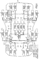
- FIG. 1 is a block diagram showing an in-vehicle network 1 as a communication system of the present invention.
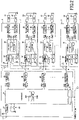
- FIG. 2 is a block diagram showing a configuration of a master device 2 and a slave device 3 constituting the in-vehicle network 1 shown in FIG. 1 .
- the in-vehicle network 1 shown in FIG. 1 is mounted in a vehicle 10.
- the in-vehicle network 1 includes a plurality of master devices 2 and a plurality of slave devices 3.
- the plurality of master devices 2 are arranged in each area of the vehicle 10.
- the master devices 2 are disposed at five locations, the center of the front of the vehicle 10, the right side of the front, the left side of the front, the right side of the rear, and the left side of the rear.
- the five master devices 2 are communicably connected to each other through a communication line L1. Further, the master devices 2 are connected to each other via a +B power supply line L2 connected to a battery (not shown), and power is supplied via the +B power supply line L2.
- each of the five master devices 2 is communicably connected to a plurality of slave devices 3 arranged in the own area through a communication line L1.
- the master device 2 and the slave devices 3 are connected one to many.
- the master device 2 controls the operations of the plurality of slave devices 3 by communicating with the plurality of slave devices 3.
- the slave device 3 is connected to a plurality of loads 20 ( FIG. 2 ) such as lamps, seat motors, door motors and the like disposed in the own area, and controls the driving of the loads 20 in accordance with communication with the master device 2.
- the slave devices 3 in the respective areas are used for +B connected to the load 20 that can be driven at all times, for ACC connected to the load 20 that can be driven when an accessory is used, and for IG connected to the load 20 that can be driven at the time of ignition.
- the plurality of master devices 2 has the same configuration, and each of the plurality of master devices 2 has an interface (hereinafter referred to as I/F) 21, a power supply circuit 22, a plurality of local SWs 23, a microcomputer 24, a plurality of semiconductor relays CH21 to C2n as a switch.
- I/F interface
- I/F power supply circuit
- microcomputer microcomputer
- the I/F 21 is a communication interface for communicating with another master device 2 and a plurality of slave devices 3.
- the I/F 21 is an interface capable of inputting and outputting signals corresponding to various communications (CAN, LIN, and other communication methods).
- the power supply circuit 22 is a circuit that generates a power supply for the microcomputer 24 to be described later from the power supplied from the +B power supply line L2 and supplies power to the microcomputer 24.
- the local SW 23 is operated by the user to operate the load 20.
- the microcomputer 24 is composed of a well-known CPU (Central Processing Unit) 24A and a flash ROM (Read Only Memory) 24B.
- the CPU 24A controls the entire master device 2 and performs various processes according to the processing program.
- the flash ROM 24B is a memory for storing the ID of the slave device 3 connected to the master device 2, the program of processing to be executed by the CPU 24A, and the like.
- the semiconductor relays CH21 to CH2n are provided for each of the plurality of slave devices 3 in a one-to-one correspondence.
- the semiconductor relays CH21 to CH2n are connected to the slave devices 3 for +B, ACC, and IG via the +B power supply line L3, the ACC power supply line L4, and the IG power supply line L5.
- the semiconductor relays CH21 to CH2n are turned on when a drive signal is outputted from the microcomputer 24 to supply power from the +B power supply line L2 via the +B power supply line L3, the ACC power supply line L4, and the IG power supply line L5 to the corresponding slave device 3.
- the semiconductor relays CH21 to CH2n have a current detection function for detecting a current flowing in the semiconductor relays CH21 to CH2n, and the detected currents are input to the microcomputer 24.
- the plurality of slave devices 3 has the same configuration and each has an I/F 31, a power supply circuit 32, a microcomputer 33, a plurality of local SWs 34, and a plurality of semiconductor relays CH31 to CH38.
- the I/F 31 is an interface for communicating with the master device 2, and capable of inputting and outputting signals corresponding to various communications (CAN, LIN, and other communication methods).
- the power supply circuit 32 is a circuit that generates a power supply for a microcomputer 33 to be described later from power supplied from the +B power supply line L3, the ACC power supply line L4, and the IG power supply line L5 and supplies power to the microcomputer 33.
- the microcomputer 33 is composed of a CPU 33A and a flash ROM 33B.
- the CPU 33A controls the entire slave device 3 and performs various processes according to the processing program.
- the flash ROM 33B is a memory for storing an initial ID, a program, a variable, and a setting value of processing to be executed by the CPU 33A, and in the initial state, the same contents are written in all the slave devices 3.
- the initial ID is a temporary ID, and a transmission initial ID and a reception initial ID are set.
- the processing program of the CPU 33A includes a communication program for communicating with the master device 2 connected via the communication line L1 and a system operation program necessary for system operation.
- the operation program of the load 20 is not written in the flash ROM 33B in the initial state, but is written after setting the ID.
- the plurality of local SWs 34 are connected to the microcomputer 33 and input ON/OFF information to the microcomputer 33.
- the plurality of semiconductor relays CH31 to CH38 are connected between the microcomputer 33 and the loads 20, respectively, and are turned on and off in accordance with a drive signal from the microcomputer 33. When the semiconductor relays CH31 to CH38 turn on, the power from the +B power supply line L3, the ACC power supply line L4, and the IG power supply line L5 are supplied to the loads 20.
- the semiconductor relays CH31 to CH38 have a current detection function for detecting the current flowing in the semiconductor relays CH31 to CH38, and the detected currents are input to the microcomputer 33.
- the number of the semiconductor relays CH31 to CH38 provided for the slave device 3 is eight as an example, but the present invention is not limited to this and any number may be used. All the slave devices 3 have the same number of semiconductor relays CH1 to CH8.
- the first bit10 to bit0 represents the identification information (ID) of the slave device 3.
- ID the identification information
- the identification information is allocated to all the slave devices 3 arranged in the vehicle 10 without overlapping.
- the identification information is composed of installation information, reserve information, transmission/reception information, and slave type information.
- Bit10 to bit7 are allocated to the installation information.
- Bit10 to bit9 represent installation positions in the traveling direction of the vehicle, and become “01” if the installation position of the slave device 3 is on the front side of the vehicle, “10” if on the rear side, and “11” if at the center in the traveling direction.
- Bit8 to bit7 represent installation positions in the left-right direction of the vehicle 10, and become “01” if the installation position of the slave device 3 is on the right side of the vehicle 10, "10” in the case of the left side, and “11” in the case of the center in the left-right direction.
- Bit6 is allocated to reserve information,.
- the reserve information is always "0".
- Bit5 is allocated to the transmission/reception information, becomes “1" when the slave device 3 transmits to the master device 2, and becomes “0" when the slave device 3 receives from the master device 2.
- Bit4 to bit0 are allocated to the slave type information.
- the slave type information is information that is allocated without overlapping with a plurality of slave devices 3 connected to the same master device 2 (but may overlap between the slave devices 3 connected to different master devices 2).
- Bit7 to bit0 following the ID indicate load control information after ID setting.
- Bit 7 to bit 0 are allocated to the semiconductor relays CH38 to CH31 respectively.
- each bit n (n is any integer from 0 to 7) is “0”, it represents “off” of the semiconductor relay CH 3n+1 assigned to the bit n.
- each bit n (n is any integer from 0 to 7) is “1”, it represents "on” of the semiconductor relay CH 3n+1 assigned to the bit n.
- bit 7 indicates success (OK) and failure (NG) of ID setting which will be described later, and bit 6 to bit 0 are blank.
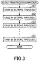
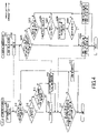
- the ID setting operation of the in-vehicle network 1 having the above-described configuration will be described with reference to the flowcharts of FIGS. 3 to 4 .
- the same initial ID in the initial state (ID is not set), the same initial ID (initial reception ID, initial transmission ID) is set in all the slave devices 3 and stored in the ID area of the flash ROM 33B.
- IDs set in the slave device 3 There are two types of IDs set in the slave device 3: a reception ID and a transmission ID, but since the difference between the two is only the transmission/reception information (bit5 of ID) as shown in Table 1, If either is determined, the transmission/reception ID is naturally determined.
- the setting of the reception ID will be described, and as the initial reception ID, it is assumed that "00000011111" which is "0" for bit10 to bit5 and "1" for bit4 to bit0 is set as shown in the following Table 2.
- ID installation information reserve transmission /reception slave type information bit10 bit9 bit8 bit7 bit6 bit5 bit4 bit3 bit2 bit1 bit0 0 0 0 0 0 0 0 1 1 1 1
- the reception ID and the transmission ID corresponding to the semiconductor relays CH21 to CH2n are stored in the flash ROM 24B or the like in advance in all the master devices 2.
- the installation information of the reception ID and the transmission ID are all set to the same value regardless of the semiconductor relays CH21 to CH2n.
- the installation information of the ID is "0101" as shown in the following Tables 3 and 4.
- values corresponding to the semiconductor relays CH21 to CH2n are stored. For example, "00001”, “00010”,... are set as slave type information corresponding to the semiconductor relays CH21, CH22. In this case, as shown in Tables 3 and 4 above, "01010000001”, “01010000010”,... are stored as the reception IDs corresponding to the semiconductor relays CH21, CH22 ..., and "01010100001”, “01010100010” ... are stored as the transmission IDs.
- the microcomputer 24 (hereinafter may be simply referred to as the master device 2) of the master device 2 executes the ID setting process shown in FIG. 3 after starting, and the ID setting processing (steps S1 to Sn) of the slave devices 3 connected to the semiconductor relays CH21 to CH2n in order.
- the master device 2 In the ID setting process of the slave device 3 connected to the semiconductor relay CH21, the master device 2 first turns on the semiconductor relay CH21 (step S1 in FIG. 3 ). Power is supplied to the slave device 3 connected to the semiconductor relay CH21 in response to turning on of the semiconductor relay CH21.
- the microcomputer 33 (hereinafter may be simply referred to as the slave device 3) of the slave device 3 connected to the semiconductor relay CH21 is activated when power is supplied and executes the ID setting process shown in FIG. 4 .
- the slave device 3 first reads its own ID stored in the ID area of the flash ROM 33B (step S 201). Next, the slave device 3 transmits the read ID (step S202).
- step S12 If the master device 2 cannot receive the ID within the predetermined time T1 after turning on the semiconductor relay CH21 in step S11 (step S12), the master device 2 determines that there is no slave device 3 connected to the semiconductor relay CH21, and after stopping the ID setting (Step S18), and ends the process. On the other hand, when receiving the ID within the predetermined time T1 (Y in step S12), the master device 2 determines whether the received ID is the initial ID (step S13).
- the master device 2 determines whether the received ID is different from the ID (01010000001 in the example shown in Table 3) corresponding to the semiconductor relay CH21 stored in the flash ROM 24B (Step S14). If the two match (N in step S14), the ID setting unnecessary signal is transmitted with the matching ID "01010000001" (step S15), and the flow proceeds to step S17.
- the ID setting unnecessary signal is a signal in which the bit 7 of the byte is set to "1" and the bit 6 to the bit 0 to "0" to the matched ID as shown in the following Table 5.
- ID installation information reserve transmission /reception slave type information bit10 bit9 bit8 bit7 bit6 bit5 bit4 bit3 bit2 bit1 bit0 0 1 0 1 0 0 0 0 0 0 0 1 byte bit7 bit6 bit5 bit4 bit3 bit2 bit1 bit0 1 0 0 0 0 0 0 0 0 0 0 0
- step S13 if the ID received in step S13 is the initial ID (Y in step S13), the master device 2 proceeds to step S16. Even if the received ID and the ID corresponding to the semiconductor relay CH 21 stored in the flash ROM 24B are different (Y in step S 14), the master device 2 also proceeds to step S16.
- step S16 the CPU 24A of the master device 2 functions as a transmitter, reads the ID corresponding to the semiconductor relay CH21 from the flash ROM 24B, and transmits the read ID.
- the CPU 24A sets the bit 7 of the byte to be transmitted together with the ID to "0".
- ID installation information reserve transmission /reception slave type information bit10 bit9 bit8 bit7 bit6 bit5 bit4 bit3 bit2 bit1 bit0 0 1 0 1 0 0 0 0 0 0 0 1 byte bit7 bit6 bit5 bit4 bit3 bit1 bit0 0 0 0 0 0 0 0 0 0 0 0 0 0 0 0 0 0
- the slave device 3 When the slave device 3 receives an ID setting unnecessary signal (that is, a signal of which bit 7 of byte is "1") within a predetermined time T2 after transmitting the ID (Y in step S 203), the slave device 3 transmits the ID written in the ID area (ID setting OK) (step 204), and finishes the ID setting process.
- ID setting OK has the same configuration as the ID setting unnecessary signal shown in Table 5, and is a signal with bit 7 of byte set to "1".
- the slave device 3 when receiving the ID (that is, the signal of bit 7 of byte being "0") within the predetermined time T2 (Y at step S 205), the slave device 3 erases the initial ID from the ID area of the flash ROM 33B S206). When the erasure of the ID area of the flash ROM 33B succeeds (Y in step S207), the CPU 33A of the slave device 3 functions as a setting unit and writes the received reception ID in the ID area of the flash ROM 33B (step S208).
- step S209 when the received ID matches the received ID written in the flash ROM 33B and the writing is determined to be successful (Y in step S209), the slave device 3 proceeds to step S204.
- step S204 the slave device 3 transmits an ID setting end signal (ID setting OK) with the ID written in the flash ROM 33B.
- the ID setting end signal (ID setting OK) is a signal whose bit 7 of the byte is "1" as shown in Table 5.
- step S205 when the slave device 3 cannot receive the ID within the predetermined time T2 (N in step S205), when the erasure of the flash ROM 33B fails (N in step S207), or when the ID writing fails (N in step S209), the process proceeds to step S210.
- step S210 the slave device 3 transmits an ID setting end signal (ID setting NG) with the initial ID.
- the ID setting end signal (ID setting NG) is a signal whose bit 7 of the byte is "0" as shown in the following Table 7.
- ID installation information reserve transmission /reception slave type information bit10 bit9 bit8 bit7 bit6 bit5 bit4 bit3 bit2 bit1 bit0 0 0 0 0 0 0 0 1 1 1 1 1 byte bit7 bit6 bit5 bit4 bit3 bit2 bit1 bit0 0 0 0 1 0 0 0 0 0 0 0
- the master device 2 When the master device 2 receives the ID setting end signal (ID setting OK) within the predetermined time T3 after transmitting the ID or the ID setting unnecessary signal, if the ID matches the ID transmitted in the steps S16 and S15 (step Y in S17), the processing is terminated.
- ID setting OK the ID setting end signal
- step S18 when the master device 2 cannot receive the ID setting end signal (ID setting OK) within the predetermined time T3 or if the ID does not match the ID transmitted in S16 and S15 even if the ID can be received (N in step S17), the ID setting is canceled (step S18), and the process is terminated.
- ID setting OK the ID setting end signal
- step S2 to Sn the ID setting process (steps S2 to Sn) of the slave device 3 connected to the semiconductor relays CH22 to CH2n will be described.
- the master device 2 is the same as the ID setting process of the slave device 3 connected to the semiconductor relay CH21 and therefore will be briefly described.
- the master device 2 turns on the semiconductor relays CH22 to CH2n instead of turning on the semiconductor relay CH21 in step S11.
- the slave device 3 executes the above-described ID setting process.
- the master device 2 is provided with a plurality of semiconductor relays CH21 to CH2n provided for each of the plurality of slave devices 3 and supplying power to the corresponding slave device 3, and the flash ROM 24B that stores an ID corresponding to the plurality of semiconductor relays CH21 to CH2n.
- the master device 2 turned on the semiconductor relays CH21 to CH2n sequentially and transmits the corresponding ID each time the semiconductor relays CH21 to CH2n are turned on.
- the slave device 3 sets the ID received after power supply as its own ID. That is, according to the present embodiment, after the master device 2 and the slave device 3 are assembled and connected to the in-vehicle network 1, ID setting can be performed by turning on and off the semiconductor relays CH21 to CH2n. Thereby, since it is not necessary to assign an ID each time the slave device 3 is connected (assembled), it is possible to shorten the setting time of the ID and to reduce erroneous settings.
- the master device 2 is installed in the vehicle 10, and the plurality of slave devices 3 are connected to the plurality of loads 20.
- the plurality of loads 20 are classified into a load 20 that can be driven at all times, a load 20 that can be driven when an accessory is used, and a load 20 that can be driven at the time of ignition. Then, the same kind of load 20 is connected to one slave device 3.
- a plurality of master devices 2 are installed in the vehicle 10, and the IDs stored in the flash ROM 24B include installation information indicating the installation position of the master device 2 in the vehicle.
- the IDs stored in the flash ROM 24B include installation information indicating the installation position of the master device 2 in the vehicle.
Landscapes
- Engineering & Computer Science (AREA)
- Computer Networks & Wireless Communication (AREA)
- Signal Processing (AREA)
- Theoretical Computer Science (AREA)
- Physics & Mathematics (AREA)
- General Engineering & Computer Science (AREA)
- Mechanical Engineering (AREA)
- General Physics & Mathematics (AREA)
- Mathematical Physics (AREA)
- Computer Hardware Design (AREA)
- Medical Informatics (AREA)
- General Health & Medical Sciences (AREA)
- Computing Systems (AREA)
- Health & Medical Sciences (AREA)
- Small-Scale Networks (AREA)
- Remote Monitoring And Control Of Power-Distribution Networks (AREA)
- Selective Calling Equipment (AREA)
Claims (4)
- Système de communication comprenant une pluralité de dispositifs esclaves (3) et un dispositif maître (2) qui communique avec la pluralité de dispositifs esclaves (3),dans lequel le dispositif maître (2) comprend :une pluralité de commutateurs (CH21-CH2n) fournis pour chacun de la pluralité de dispositifs esclaves (3), pour alimenter en courant les dispositifs esclaves (3) correspondants ;une unité de stockage (24B) destinée au stockage d'informations d'identification correspondant à la pluralité de commutateurs (3) ; etune unité de transmission (24A) ;caractérisé en ce quel'unité de transmission (24A) transmet des informations d'identification correspondantes chaque fois que le commutateur (CH21-CH2n) est activé par activation séquentielle du commutateur (CH21-CH2n), etdans lequel la pluralité de dispositifs esclaves (3) possède une unité de réglage (33A) qui établit les informations d'identification reçues après l'alimentation en courant en tant que ses propres informations d'identification.
- Système de communication selon la revendication 1,dans lequel le dispositif maître (2) est installé dans un véhicule,dans lequel la pluralité de dispositifs esclaves (3) est connectée à une pluralité de charges (20),dans lequel les charges de la pluralité de charges (20) sont classées en charge qui peut être entraînée à tout moment, charge qui peut être entraînée lorsqu'un accessoire est utilisé, et charge qui peut être entraînée au moment de l'allumage, etdans lequel les charges (20) du même type sont connectées à l'un des dispositifs esclaves (3).
- Système de communication selon la revendication 1 ou 2,dans lequel une pluralité des dispositifs maîtres (2) est installée dans un véhicule, etdans lequel les informations d'identification stockées dans l'unité de stockage (23B) comprennent des informations d'installation indiquant une position d'installation du dispositif maître (2) dans le véhicule.
- Dispositif maître communiquant avec une pluralité de dispositifs esclaves (3), comprenant :une pluralité de commutateurs (CH21-CH2n) fournis pour chacun de la pluralité de dispositifs esclaves (3) et alimentant en courant les dispositifs esclaves (3) correspondants ;une unité de stockage (24B) destinée au stockage d'informations d'identification correspondant à la pluralité de commutateurs (3) ; etune unité de transmission (24A) ;caractérisé en ce quel'unité de transmission (24A) transmet des informations d'identification correspondantes qui correspondent aux commutateurs (CH21-CH2n) chaque fois que les commutateurs (CH21-CH2n) sont activés par activation séquentielle des commutateurs (CH21-CH2n).
Applications Claiming Priority (1)
| Application Number | Priority Date | Filing Date | Title |
|---|---|---|---|
| JP2018084309A JP7046700B2 (ja) | 2018-04-25 | 2018-04-25 | 通信システム |
Publications (2)
| Publication Number | Publication Date |
|---|---|
| EP3560767A1 EP3560767A1 (fr) | 2019-10-30 |
| EP3560767B1 true EP3560767B1 (fr) | 2022-05-04 |
Family
ID=65995621
Family Applications (1)
| Application Number | Title | Priority Date | Filing Date |
|---|---|---|---|
| EP19165668.5A Active EP3560767B1 (fr) | 2018-04-25 | 2019-03-28 | Système de communication |
Country Status (4)
| Country | Link |
|---|---|
| US (1) | US11153114B2 (fr) |
| EP (1) | EP3560767B1 (fr) |
| JP (1) | JP7046700B2 (fr) |
| CN (1) | CN110401690B (fr) |
Families Citing this family (1)
| Publication number | Priority date | Publication date | Assignee | Title |
|---|---|---|---|---|
| DE102020124549A1 (de) * | 2020-09-21 | 2022-03-24 | Bayerische Motoren Werke Aktiengesellschaft | System zur datenübertragung in einem kraftfahrzeug, kraftfahrzeug und verfahren |
Family Cites Families (40)
| Publication number | Priority date | Publication date | Assignee | Title |
|---|---|---|---|---|
| IT1232090B (it) * | 1989-05-04 | 1992-01-23 | Sgs Thomson Microelectronics | Sistema di collegamento tra un unita di elaborazione principale e del le unita periferiche |
| US5053964A (en) * | 1989-07-17 | 1991-10-01 | Utdc, Inc. | On-board integrated vehicle control and communication system |
| US5305316A (en) * | 1990-09-04 | 1994-04-19 | Nissan Motor Co., Ltd. | Multiplex communication system |
| JPH04326897A (ja) * | 1991-04-26 | 1992-11-16 | Pioneer Electron Corp | 車載用データ通信システム |
| JP3578058B2 (ja) * | 2000-07-13 | 2004-10-20 | 株式会社デンソー | 多重通信システム |
| DE10236879B4 (de) * | 2001-08-14 | 2013-10-24 | Denso Corporation | Hindernis-Detektionsgerät und damit in Beziehung stehendes Kommunikationsgerät |
| DE60301752T9 (de) * | 2002-04-16 | 2006-11-23 | Robert Bosch Gmbh | Verfahren zur Überwachung einer Zugriffsablaufsteuerung für ein Kommunikationsmedium einer Kommunikationssteuerung eines Kommunikationssystems |
| JP3988753B2 (ja) * | 2004-07-02 | 2007-10-10 | 株式会社デンソー | 通信装置 |
| JP2007215102A (ja) * | 2006-02-13 | 2007-08-23 | Denso Corp | 通信装置 |
| JP4656421B2 (ja) * | 2006-02-28 | 2011-03-23 | 株式会社デンソー | バス通信システム |
| JP4737049B2 (ja) * | 2006-11-27 | 2011-07-27 | 株式会社デンソー | 通信システム及び電子制御装置 |
| US20080239984A1 (en) * | 2007-03-26 | 2008-10-02 | Kevin Le | Energy Saving System/Network |
| JP2009292290A (ja) * | 2008-06-04 | 2009-12-17 | Fujitsu Ten Ltd | 制御装置及び制御方法 |
| US20100262296A1 (en) * | 2008-06-25 | 2010-10-14 | HID Laboratories, Inc. | Lighting control system and method |
| JP2010184575A (ja) | 2009-02-12 | 2010-08-26 | Sanden Corp | 車載機器制御システム |
| CN101559744A (zh) * | 2009-05-21 | 2009-10-21 | 南京工业职业技术学院 | 蓝牙技术在汽车门控和点火系统中的应用 |
| DE102010053803B3 (de) * | 2010-12-08 | 2012-02-23 | Brose Fahrzeugteile Gmbh & Co. Kommanditgesellschaft, Hallstadt | Verfahren zum Betrieb eines Bordnetzes eines Kraftfahrzeugs sowie danach arbeitendes Bussystem |
| KR101814487B1 (ko) * | 2011-06-07 | 2018-01-04 | 현대모비스 주식회사 | 카메라 위치 판별 장치 및 방법 |
| JP5598429B2 (ja) | 2011-06-22 | 2014-10-01 | 株式会社オートネットワーク技術研究所 | 電源制御システム、電源制御装置及び電源制御方法 |
| AU2011226785A1 (en) * | 2011-09-21 | 2013-04-04 | Imprenditore Pty Limited | Power Monitoring and Signal Unit |
| CN103946829B (zh) * | 2011-10-05 | 2016-09-21 | 美国亚德诺半导体公司 | 用于高速数据和电力分配的双线通信系统 |
| US9727511B2 (en) * | 2011-12-30 | 2017-08-08 | Bedrock Automation Platforms Inc. | Input/output module with multi-channel switching capability |
| JP5741496B2 (ja) * | 2012-03-14 | 2015-07-01 | 株式会社オートネットワーク技術研究所 | 車載通信システム |
| US9946675B2 (en) * | 2013-03-13 | 2018-04-17 | Atieva, Inc. | Fault-tolerant loop for a communication bus |
| CN111181732B (zh) * | 2014-05-08 | 2024-10-01 | 松下电器(美国)知识产权公司 | 车载网络系统、电子控制单元及不正常检测方法 |
| EP3152666B1 (fr) * | 2014-06-04 | 2021-05-19 | Moduware PTY LTD | Système super concentrateur et procédé correspondant |
| JP6430749B2 (ja) * | 2014-08-18 | 2018-11-28 | ラピスセミコンダクタ株式会社 | 電源供給システム |
| JP6503911B2 (ja) * | 2015-06-17 | 2019-04-24 | マツダ株式会社 | 車両用情報通信システム |
| JP6477281B2 (ja) * | 2015-06-17 | 2019-03-06 | 株式会社オートネットワーク技術研究所 | 車載中継装置、車載通信システム及び中継プログラム |
| US10116749B2 (en) * | 2015-08-31 | 2018-10-30 | The Boeing Company | Method for providing flight management system data to peripheral devices |
| JP6487814B2 (ja) * | 2015-09-09 | 2019-03-20 | 株式会社Soken | 車両用検知システム |
| CN105416209B (zh) * | 2015-12-07 | 2017-11-10 | 安徽江淮汽车集团股份有限公司 | 一种自动预置用户车辆个性化配置的车载系统及方法 |
| CN107025191A (zh) * | 2016-01-30 | 2017-08-08 | 鸿富锦精密电子(重庆)有限公司 | 电子装置连接系统 |
| CN107025194A (zh) * | 2016-01-30 | 2017-08-08 | 鸿富锦精密电子(重庆)有限公司 | 电子装置供电系统 |
| KR102400730B1 (ko) * | 2016-02-23 | 2022-05-20 | 현대자동차주식회사 | 네트워크에서 통신 노드들 간의 시간 동기화 방법 |
| WO2018026030A1 (fr) * | 2016-08-03 | 2018-02-08 | 엘지전자 주식회사 | Véhicule, et procédé de commande associé |
| US12164456B2 (en) * | 2016-08-25 | 2024-12-10 | Analog Devices, Inc. | Systems and techniques for remote bus enable |
| JP2018120422A (ja) * | 2017-01-25 | 2018-08-02 | ルネサスエレクトロニクス株式会社 | 車載通信システム、ドメインマスタ、及びファームウェア更新方法 |
| US10430358B2 (en) * | 2017-03-30 | 2019-10-01 | Mitac Computing Technology Corporation | High-definition multimedia interface apparatus capable of communication with slave/master apparatus utilizing the same HDMI port and method for controlling the same |
| CN107147994B (zh) * | 2017-06-09 | 2020-05-05 | 厦门盈趣科技股份有限公司 | 基于语音终端的zigbee网关装置 |
-
2018
- 2018-04-25 JP JP2018084309A patent/JP7046700B2/ja active Active
-
2019
- 2019-02-15 US US16/277,369 patent/US11153114B2/en active Active
- 2019-03-28 EP EP19165668.5A patent/EP3560767B1/fr active Active
- 2019-04-25 CN CN201910338309.4A patent/CN110401690B/zh active Active
Also Published As
| Publication number | Publication date |
|---|---|
| CN110401690B (zh) | 2022-06-10 |
| JP2019193113A (ja) | 2019-10-31 |
| US11153114B2 (en) | 2021-10-19 |
| CN110401690A (zh) | 2019-11-01 |
| JP7046700B2 (ja) | 2022-04-04 |
| US20190334739A1 (en) | 2019-10-31 |
| EP3560767A1 (fr) | 2019-10-30 |
Similar Documents
| Publication | Publication Date | Title |
|---|---|---|
| EP3561683B1 (fr) | Attribution d'identifications dans un système de communication | |
| US11082253B2 (en) | Communication system | |
| US10887128B2 (en) | In-vehicle network system | |
| US7668991B2 (en) | Address assignment to plurality of connecting elements in a bus system | |
| US20160288741A1 (en) | Wireless Electrical Interface System | |
| US20190098558A1 (en) | Communication managing device and communication system | |
| EP4018331B1 (fr) | Procédé et système d'auto-adressage de noeuds sur un bus de communication | |
| US20220029855A1 (en) | Relay device system | |
| EP3560767A1 (fr) | Système de communication | |
| US10812288B2 (en) | Communication system | |
| US10848378B2 (en) | Setting device and computer | |
| US10972307B2 (en) | Communication system | |
| EP0917991B1 (fr) | Système de communication multiplexé de vehicule et méthode de fabrication | |
| EP4289154B1 (fr) | Système et procédé de communication | |
| US5583770A (en) | Electronic control apparatus for failure diagnosis | |
| JP4591383B2 (ja) | バス通信システム | |
| AU730730B2 (en) | Control device for an authorisation system | |
| JP2010095134A (ja) | 通信中継装置 | |
| KR100478784B1 (ko) | 시스템 간의 내부 통신장치 | |
| EP4102779A1 (fr) | Système de communication, dispositif de commande supérieur et dispositif de commande subordonné | |
| US7917738B2 (en) | Method and base chip for monitoring the operation of a microcontroller unit | |
| JP2016208474A (ja) | 通信システム及び通信制御装置 | |
| JP2022135493A (ja) | 通信システム、管理装置、端末装置 |
Legal Events
| Date | Code | Title | Description |
|---|---|---|---|
| PUAI | Public reference made under article 153(3) epc to a published international application that has entered the european phase |
Free format text: ORIGINAL CODE: 0009012 |
|
| STAA | Information on the status of an ep patent application or granted ep patent |
Free format text: STATUS: REQUEST FOR EXAMINATION WAS MADE |
|
| 17P | Request for examination filed |
Effective date: 20190328 |
|
| AK | Designated contracting states |
Kind code of ref document: A1 Designated state(s): AL AT BE BG CH CY CZ DE DK EE ES FI FR GB GR HR HU IE IS IT LI LT LU LV MC MK MT NL NO PL PT RO RS SE SI SK SM TR |
|
| AX | Request for extension of the european patent |
Extension state: BA ME |
|
| RBV | Designated contracting states (corrected) |
Designated state(s): AL AT BE BG CH CY CZ DE DK EE ES FI FR GB GR HR HU IE IS IT LI LT LU LV MC MK MT NL NO PL PT RO RS SE SI SK SM TR |
|
| GRAP | Despatch of communication of intention to grant a patent |
Free format text: ORIGINAL CODE: EPIDOSNIGR1 |
|
| STAA | Information on the status of an ep patent application or granted ep patent |
Free format text: STATUS: GRANT OF PATENT IS INTENDED |
|
| INTG | Intention to grant announced |
Effective date: 20211222 |
|
| RAP3 | Party data changed (applicant data changed or rights of an application transferred) |
Owner name: YAZAKI CORPORATION |
|
| GRAS | Grant fee paid |
Free format text: ORIGINAL CODE: EPIDOSNIGR3 |
|
| GRAA | (expected) grant |
Free format text: ORIGINAL CODE: 0009210 |
|
| STAA | Information on the status of an ep patent application or granted ep patent |
Free format text: STATUS: THE PATENT HAS BEEN GRANTED |
|
| AK | Designated contracting states |
Kind code of ref document: B1 Designated state(s): AL AT BE BG CH CY CZ DE DK EE ES FI FR GB GR HR HU IE IS IT LI LT LU LV MC MK MT NL NO PL PT RO RS SE SI SK SM TR |
|
| REG | Reference to a national code |
Ref country code: GB Ref legal event code: FG4D |
|
| REG | Reference to a national code |
Ref country code: CH Ref legal event code: EP |
|
| REG | Reference to a national code |
Ref country code: AT Ref legal event code: REF Ref document number: 1488741 Country of ref document: AT Kind code of ref document: T Effective date: 20220515 |
|
| REG | Reference to a national code |
Ref country code: DE Ref legal event code: R096 Ref document number: 602019014330 Country of ref document: DE |
|
| REG | Reference to a national code |
Ref country code: IE Ref legal event code: FG4D |
|
| REG | Reference to a national code |
Ref country code: LT Ref legal event code: MG9D |
|
| REG | Reference to a national code |
Ref country code: NL Ref legal event code: MP Effective date: 20220504 |
|
| REG | Reference to a national code |
Ref country code: AT Ref legal event code: MK05 Ref document number: 1488741 Country of ref document: AT Kind code of ref document: T Effective date: 20220504 |
|
| PG25 | Lapsed in a contracting state [announced via postgrant information from national office to epo] |
Ref country code: SE Free format text: LAPSE BECAUSE OF FAILURE TO SUBMIT A TRANSLATION OF THE DESCRIPTION OR TO PAY THE FEE WITHIN THE PRESCRIBED TIME-LIMIT Effective date: 20220504 Ref country code: PT Free format text: LAPSE BECAUSE OF FAILURE TO SUBMIT A TRANSLATION OF THE DESCRIPTION OR TO PAY THE FEE WITHIN THE PRESCRIBED TIME-LIMIT Effective date: 20220905 Ref country code: NO Free format text: LAPSE BECAUSE OF FAILURE TO SUBMIT A TRANSLATION OF THE DESCRIPTION OR TO PAY THE FEE WITHIN THE PRESCRIBED TIME-LIMIT Effective date: 20220804 Ref country code: NL Free format text: LAPSE BECAUSE OF FAILURE TO SUBMIT A TRANSLATION OF THE DESCRIPTION OR TO PAY THE FEE WITHIN THE PRESCRIBED TIME-LIMIT Effective date: 20220504 Ref country code: LT Free format text: LAPSE BECAUSE OF FAILURE TO SUBMIT A TRANSLATION OF THE DESCRIPTION OR TO PAY THE FEE WITHIN THE PRESCRIBED TIME-LIMIT Effective date: 20220504 Ref country code: HR Free format text: LAPSE BECAUSE OF FAILURE TO SUBMIT A TRANSLATION OF THE DESCRIPTION OR TO PAY THE FEE WITHIN THE PRESCRIBED TIME-LIMIT Effective date: 20220504 Ref country code: GR Free format text: LAPSE BECAUSE OF FAILURE TO SUBMIT A TRANSLATION OF THE DESCRIPTION OR TO PAY THE FEE WITHIN THE PRESCRIBED TIME-LIMIT Effective date: 20220805 Ref country code: FI Free format text: LAPSE BECAUSE OF FAILURE TO SUBMIT A TRANSLATION OF THE DESCRIPTION OR TO PAY THE FEE WITHIN THE PRESCRIBED TIME-LIMIT Effective date: 20220504 Ref country code: ES Free format text: LAPSE BECAUSE OF FAILURE TO SUBMIT A TRANSLATION OF THE DESCRIPTION OR TO PAY THE FEE WITHIN THE PRESCRIBED TIME-LIMIT Effective date: 20220504 Ref country code: BG Free format text: LAPSE BECAUSE OF FAILURE TO SUBMIT A TRANSLATION OF THE DESCRIPTION OR TO PAY THE FEE WITHIN THE PRESCRIBED TIME-LIMIT Effective date: 20220804 Ref country code: AT Free format text: LAPSE BECAUSE OF FAILURE TO SUBMIT A TRANSLATION OF THE DESCRIPTION OR TO PAY THE FEE WITHIN THE PRESCRIBED TIME-LIMIT Effective date: 20220504 |
|
| PG25 | Lapsed in a contracting state [announced via postgrant information from national office to epo] |
Ref country code: RS Free format text: LAPSE BECAUSE OF FAILURE TO SUBMIT A TRANSLATION OF THE DESCRIPTION OR TO PAY THE FEE WITHIN THE PRESCRIBED TIME-LIMIT Effective date: 20220504 Ref country code: PL Free format text: LAPSE BECAUSE OF FAILURE TO SUBMIT A TRANSLATION OF THE DESCRIPTION OR TO PAY THE FEE WITHIN THE PRESCRIBED TIME-LIMIT Effective date: 20220504 Ref country code: LV Free format text: LAPSE BECAUSE OF FAILURE TO SUBMIT A TRANSLATION OF THE DESCRIPTION OR TO PAY THE FEE WITHIN THE PRESCRIBED TIME-LIMIT Effective date: 20220504 Ref country code: IS Free format text: LAPSE BECAUSE OF FAILURE TO SUBMIT A TRANSLATION OF THE DESCRIPTION OR TO PAY THE FEE WITHIN THE PRESCRIBED TIME-LIMIT Effective date: 20220904 |
|
| PG25 | Lapsed in a contracting state [announced via postgrant information from national office to epo] |
Ref country code: SM Free format text: LAPSE BECAUSE OF FAILURE TO SUBMIT A TRANSLATION OF THE DESCRIPTION OR TO PAY THE FEE WITHIN THE PRESCRIBED TIME-LIMIT Effective date: 20220504 Ref country code: SK Free format text: LAPSE BECAUSE OF FAILURE TO SUBMIT A TRANSLATION OF THE DESCRIPTION OR TO PAY THE FEE WITHIN THE PRESCRIBED TIME-LIMIT Effective date: 20220504 Ref country code: RO Free format text: LAPSE BECAUSE OF FAILURE TO SUBMIT A TRANSLATION OF THE DESCRIPTION OR TO PAY THE FEE WITHIN THE PRESCRIBED TIME-LIMIT Effective date: 20220504 Ref country code: EE Free format text: LAPSE BECAUSE OF FAILURE TO SUBMIT A TRANSLATION OF THE DESCRIPTION OR TO PAY THE FEE WITHIN THE PRESCRIBED TIME-LIMIT Effective date: 20220504 Ref country code: DK Free format text: LAPSE BECAUSE OF FAILURE TO SUBMIT A TRANSLATION OF THE DESCRIPTION OR TO PAY THE FEE WITHIN THE PRESCRIBED TIME-LIMIT Effective date: 20220504 Ref country code: CZ Free format text: LAPSE BECAUSE OF FAILURE TO SUBMIT A TRANSLATION OF THE DESCRIPTION OR TO PAY THE FEE WITHIN THE PRESCRIBED TIME-LIMIT Effective date: 20220504 |
|
| REG | Reference to a national code |
Ref country code: DE Ref legal event code: R097 Ref document number: 602019014330 Country of ref document: DE |
|
| PLBE | No opposition filed within time limit |
Free format text: ORIGINAL CODE: 0009261 |
|
| STAA | Information on the status of an ep patent application or granted ep patent |
Free format text: STATUS: NO OPPOSITION FILED WITHIN TIME LIMIT |
|
| PG25 | Lapsed in a contracting state [announced via postgrant information from national office to epo] |
Ref country code: AL Free format text: LAPSE BECAUSE OF FAILURE TO SUBMIT A TRANSLATION OF THE DESCRIPTION OR TO PAY THE FEE WITHIN THE PRESCRIBED TIME-LIMIT Effective date: 20220504 |
|
| 26N | No opposition filed |
Effective date: 20230207 |
|
| PG25 | Lapsed in a contracting state [announced via postgrant information from national office to epo] |
Ref country code: SI Free format text: LAPSE BECAUSE OF FAILURE TO SUBMIT A TRANSLATION OF THE DESCRIPTION OR TO PAY THE FEE WITHIN THE PRESCRIBED TIME-LIMIT Effective date: 20220504 |
|
| PG25 | Lapsed in a contracting state [announced via postgrant information from national office to epo] |
Ref country code: MC Free format text: LAPSE BECAUSE OF FAILURE TO SUBMIT A TRANSLATION OF THE DESCRIPTION OR TO PAY THE FEE WITHIN THE PRESCRIBED TIME-LIMIT Effective date: 20220504 |
|
| REG | Reference to a national code |
Ref country code: CH Ref legal event code: PL |
|
| GBPC | Gb: european patent ceased through non-payment of renewal fee |
Effective date: 20230328 |
|
| REG | Reference to a national code |
Ref country code: BE Ref legal event code: MM Effective date: 20230331 |
|
| PG25 | Lapsed in a contracting state [announced via postgrant information from national office to epo] |
Ref country code: LU Free format text: LAPSE BECAUSE OF NON-PAYMENT OF DUE FEES Effective date: 20230328 |
|
| REG | Reference to a national code |
Ref country code: IE Ref legal event code: MM4A |
|
| PG25 | Lapsed in a contracting state [announced via postgrant information from national office to epo] |
Ref country code: GB Free format text: LAPSE BECAUSE OF NON-PAYMENT OF DUE FEES Effective date: 20230328 |
|
| PG25 | Lapsed in a contracting state [announced via postgrant information from national office to epo] |
Ref country code: LI Free format text: LAPSE BECAUSE OF NON-PAYMENT OF DUE FEES Effective date: 20230331 Ref country code: IT Free format text: LAPSE BECAUSE OF FAILURE TO SUBMIT A TRANSLATION OF THE DESCRIPTION OR TO PAY THE FEE WITHIN THE PRESCRIBED TIME-LIMIT Effective date: 20220504 Ref country code: IE Free format text: LAPSE BECAUSE OF NON-PAYMENT OF DUE FEES Effective date: 20230328 Ref country code: GB Free format text: LAPSE BECAUSE OF NON-PAYMENT OF DUE FEES Effective date: 20230328 Ref country code: FR Free format text: LAPSE BECAUSE OF NON-PAYMENT OF DUE FEES Effective date: 20230331 Ref country code: CH Free format text: LAPSE BECAUSE OF NON-PAYMENT OF DUE FEES Effective date: 20230331 |
|
| PG25 | Lapsed in a contracting state [announced via postgrant information from national office to epo] |
Ref country code: BE Free format text: LAPSE BECAUSE OF NON-PAYMENT OF DUE FEES Effective date: 20230331 |
|
| PG25 | Lapsed in a contracting state [announced via postgrant information from national office to epo] |
Ref country code: BG Free format text: LAPSE BECAUSE OF FAILURE TO SUBMIT A TRANSLATION OF THE DESCRIPTION OR TO PAY THE FEE WITHIN THE PRESCRIBED TIME-LIMIT Effective date: 20220504 |
|
| PG25 | Lapsed in a contracting state [announced via postgrant information from national office to epo] |
Ref country code: BG Free format text: LAPSE BECAUSE OF FAILURE TO SUBMIT A TRANSLATION OF THE DESCRIPTION OR TO PAY THE FEE WITHIN THE PRESCRIBED TIME-LIMIT Effective date: 20220504 |
|
| PG25 | Lapsed in a contracting state [announced via postgrant information from national office to epo] |
Ref country code: CY Free format text: LAPSE BECAUSE OF FAILURE TO SUBMIT A TRANSLATION OF THE DESCRIPTION OR TO PAY THE FEE WITHIN THE PRESCRIBED TIME-LIMIT; INVALID AB INITIO Effective date: 20190328 |
|
| PG25 | Lapsed in a contracting state [announced via postgrant information from national office to epo] |
Ref country code: HU Free format text: LAPSE BECAUSE OF FAILURE TO SUBMIT A TRANSLATION OF THE DESCRIPTION OR TO PAY THE FEE WITHIN THE PRESCRIBED TIME-LIMIT; INVALID AB INITIO Effective date: 20190328 |
|
| PG25 | Lapsed in a contracting state [announced via postgrant information from national office to epo] |
Ref country code: TR Free format text: LAPSE BECAUSE OF FAILURE TO SUBMIT A TRANSLATION OF THE DESCRIPTION OR TO PAY THE FEE WITHIN THE PRESCRIBED TIME-LIMIT Effective date: 20220504 |
|
| PGFP | Annual fee paid to national office [announced via postgrant information from national office to epo] |
Ref country code: DE Payment date: 20260204 Year of fee payment: 8 |