EP3561685B1 - Dispositif et procédé pour commander un transfert d'informations à partir d'une pluralité de composants électroniques par l'intermédiaire d'un bus de communication vers un dispositif hôte - Google Patents
Dispositif et procédé pour commander un transfert d'informations à partir d'une pluralité de composants électroniques par l'intermédiaire d'un bus de communication vers un dispositif hôte Download PDFInfo
- Publication number
- EP3561685B1 EP3561685B1 EP18169882.0A EP18169882A EP3561685B1 EP 3561685 B1 EP3561685 B1 EP 3561685B1 EP 18169882 A EP18169882 A EP 18169882A EP 3561685 B1 EP3561685 B1 EP 3561685B1
- Authority
- EP
- European Patent Office
- Prior art keywords
- electronic components
- signal
- flop
- input
- processing blocks
- Prior art date
- Legal status (The legal status is an assumption and is not a legal conclusion. Google has not performed a legal analysis and makes no representation as to the accuracy of the status listed.)
- Active
Links
Images


Classifications
-
- G—PHYSICS
- G06—COMPUTING OR CALCULATING; COUNTING
- G06F—ELECTRIC DIGITAL DATA PROCESSING
- G06F13/00—Interconnection of, or transfer of information or other signals between, memories, input/output devices or central processing units
- G06F13/38—Information transfer, e.g. on bus
- G06F13/42—Bus transfer protocol, e.g. handshake; Synchronisation
- G06F13/4247—Bus transfer protocol, e.g. handshake; Synchronisation on a daisy chain bus
- G06F13/4256—Bus transfer protocol, e.g. handshake; Synchronisation on a daisy chain bus using a clocked protocol
-
- G—PHYSICS
- G06—COMPUTING OR CALCULATING; COUNTING
- G06F—ELECTRIC DIGITAL DATA PROCESSING
- G06F13/00—Interconnection of, or transfer of information or other signals between, memories, input/output devices or central processing units
- G06F13/14—Handling requests for interconnection or transfer
- G06F13/36—Handling requests for interconnection or transfer for access to common bus or bus system
- G06F13/362—Handling requests for interconnection or transfer for access to common bus or bus system with centralised access control
- G06F13/3625—Handling requests for interconnection or transfer for access to common bus or bus system with centralised access control using a time dependent access
-
- G—PHYSICS
- G06—COMPUTING OR CALCULATING; COUNTING
- G06F—ELECTRIC DIGITAL DATA PROCESSING
- G06F1/00—Details not covered by groups G06F3/00 - G06F13/00 and G06F21/00
- G06F1/04—Generating or distributing clock signals or signals derived directly therefrom
- G06F1/10—Distribution of clock signals, e.g. skew
-
- G—PHYSICS
- G06—COMPUTING OR CALCULATING; COUNTING
- G06F—ELECTRIC DIGITAL DATA PROCESSING
- G06F13/00—Interconnection of, or transfer of information or other signals between, memories, input/output devices or central processing units
- G06F13/38—Information transfer, e.g. on bus
- G06F13/42—Bus transfer protocol, e.g. handshake; Synchronisation
- G06F13/4282—Bus transfer protocol, e.g. handshake; Synchronisation on a serial bus, e.g. I2C bus, SPI bus
- G06F13/4291—Bus transfer protocol, e.g. handshake; Synchronisation on a serial bus, e.g. I2C bus, SPI bus using a clocked protocol
-
- H—ELECTRICITY
- H04—ELECTRIC COMMUNICATION TECHNIQUE
- H04N—PICTORIAL COMMUNICATION, e.g. TELEVISION
- H04N25/00—Circuitry of solid-state image sensors [SSIS]; Control thereof
- H04N25/40—Extracting pixel data from image sensors by controlling scanning circuits, e.g. by modifying the number of pixels sampled or to be sampled
-
- H—ELECTRICITY
- H04—ELECTRIC COMMUNICATION TECHNIQUE
- H04N—PICTORIAL COMMUNICATION, e.g. TELEVISION
- H04N25/00—Circuitry of solid-state image sensors [SSIS]; Control thereof
- H04N25/47—Image sensors with pixel address output; Event-driven image sensors; Selection of pixels to be read out based on image data
Definitions
- each of the processing blocks comprises one or multiple pairs of complementary transistors.
- the processing blocks may in particular be made in complementary metal-oxide-semiconductor (CMOS) technology.
- CMOS complementary metal-oxide-semiconductor
- MOSFETs metal oxide semiconductor field effect transistors
- the two transistors in the complementary pair may be symmetrical, in particular have the same or substantially the same threshold voltage. Substantially the same may mean that a process-related or application-related threshold discrepancy may exist, wherein for example the n-type transistor has a slightly lower threshold than the p-type transistor. In case of a realization in CMOS, this is regularly referred to as complementary-symmetry metal-oxide-semiconductor (or COS-MOS).
- COS-MOS complementary-symmetry metal-oxide-semiconductor
- the service path contains a Present flip-flop, a Past flip-flop, and a switching signal detector, the Present Input to the switching signal detector has a lower switching threshold than the input to the Past flip-flop, in order to avoid an omission failure.
- the service path contains a Present flip-flop and a Past flip-flop, the input to the Present flip-flop and to the skip path has a higher switching threshold than the input to the Past flip-flop, in order to prevent a collision failure.
- switching threshold refers to a threshold of an input to a complementary switching element pair that needs to be surpassed in order to allow the input signal to be registered and passed through as such by the circuit.
- this switching threshold is an unsigned, absolute value. For a rising edge authorization signal, the switching threshold is measured from the logical ,,0" value (e.g. at 0 Volts), while for a falling edge authorization signal, the switching threshold of the "upside down” circuit should be measured from the logical "1" (e.g. at 1.2 Volts).
- “higher switching threshold” means that the signal value at which a switching signal is detected is closer to 0.
- the electronic components may be arranged in a two-dimensional array.
- a first chain of processing blocks each associated with a column of electronic components of the plurality of electronic components and a second chain of processing blocks, each associated with a row of electronic components of the plurality of electronic components, may be provided.
- Fig. 1 shows a two-dimensional (2D) array 3 of electronic components, which is connected to a communication bus 4, on or through which information from each electronic component can be sent to a host (not shown in the figures) in a time-multiplexed fashion.
- the communication bus 4 is also connected to a column encoder (in the following: x encoder), which supplies the host with a column indicator (x_addr), and a row encoder (in the following: y encoder), which supplies the host with a row indicator (y_addr).
- x_addr and y_addr specify the specific electronic component which at a given time has gained access to the communication bus 4 for sending its information value to the host.
- Both the column and the row encoder can also be connected to the host device through the communication bus 4, in order to submit x_addr and y_addr through the communication bus 4 to the host device.
- a column request signal x_req(i) and a column select signal x_sel(i) are shared by all the electronic components in this column.
- the x_req(1:X) bus is updated by the signal x_sample (derived from a host generated row clock signal y_clk).
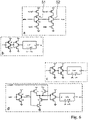
- Fig. 5 shows the service paths and the rising edge detectors of two processing blocks, the service paths of which the authorization signal travels consecutively. These are a processing block m in the chain 1, 2 of processing blocks, shown in Fig. 5a , and a next processing block n in that chain 1, 2, shown in Fig. 5b .
- the connection between the processing blocks m and n is indicated with a dotted line, in order to clarify that the there could be none or several other processing blocks in between the processing blocks m and n, as along as the authorization signal only propagates through the skip paths of these several processing blocks. Based on the above assumption, there are two ways the chain 1, 2 of processing blocks could fail due to metastable conditions: 1.
Landscapes
- Engineering & Computer Science (AREA)
- Theoretical Computer Science (AREA)
- Physics & Mathematics (AREA)
- General Engineering & Computer Science (AREA)
- General Physics & Mathematics (AREA)
- Multimedia (AREA)
- Signal Processing (AREA)
- Information Transfer Systems (AREA)
- Bus Control (AREA)
- Transforming Light Signals Into Electric Signals (AREA)
- Small-Scale Networks (AREA)
- Logic Circuits (AREA)
Claims (11)
- Un dispositif de contrôle d'un transfert d'informations d'une pluralité de composants électroniques (3) via un bus de communication (4) vers un dispositif hôte, comprenant une chaîne (1, 2) de blocs de traitement (5) connectés à la pluralité de composants électroniques (3), chacun des blocs de traitement (5) associés à l'un des composants électroniques (3) ou à un ensemble de composants électroniques de la pluralité des composants électroniques (3), dans lequel les blocs de traitement (5) sont disposés de telle sorte que, au cours du transfert d'informations, un signal d'autorisation se propage à travers la chaîne (1, 2) des blocs de traitement (5) et, lorsque le signal d'autorisation rencontre un bloc de traitement (5) associé à l'un des composants électroniques (3) ou à l'un des ensembles de composants électroniques (3) qui contient une valeur d'information à transférer, effectuant le transfert de la valeur de l'information via le bus de communication (4) vers le dispositif hôte, dans lequel les blocs de traitement (5) sont disposés pour coordonner leur traitement conformément à un signal d'horloge généré indépendamment d'un état de propagation du signal d'autorisation au sein de la chaîne (1, 2) des blocs de traitement (5), dans lequel chaque bloc de traitement comprend un chemin de service et un chemin de saut pour que le signal d'autorisation se propage le long de manière sélective, dans lequel le signal d'autorisation se propage par le chemin de service si le bloc de traitement est associé à l'un des composants électroniques ou à l'un des ensembles de composants électroniques, qui contient une valeur d'information à transférer, et se propage autrement par la voie du chemin de saut,caractérisé en ce que le chemin de service contient une bascule présente ayant une entrée et une sortie, une bascule passée ayant une entrée et une sortie, et un détecteur de signal de commutation, qui comprend une entrée présente connectée à la sortie de la bascule présente et une entrée passée connectée à la sortie de la bascule passée pour comparer la sortie de la bascule présente et la sortie de la bascule passée,dans lequel l'entrée présente du détecteur de signal de commutation a un seuil de commutation inférieur à l'entrée de la bascule passée, afin d'éviter une défaillance par omission, et/ou dans lequel l'entrée de la bascule passée a un seuil de commutation inférieur à l'entrée de la bascule présente et à l'entrée du chemin de saut, afin d'éviter une défaillance par collision.
- Le dispositif selon la revendication 1, caractérisé en ce que les blocs de traitement (5) sont disposés pour coordonner leur traitement conformément à un signal d'horloge reçu du dispositif hôte.
- Le dispositif selon la revendication 1 ou 2, caractérisé en ce que les blocs de traitement (5) sont disposés de telle sorte que le signal d'autorisation se propage à travers le bloc de traitement associé à l'un des composants électroniques ou à l'un des ensembles de composants électroniques, qui contient une valeur d'information à transférer, coordonné par le signal d'horloge reçu du dispositif hôte.
- Le dispositif selon la revendication 3, caractérisé en ce que les blocs de traitement sont disposés de telle sorte que le signal d'autorisation est propagé à travers au plus un bloc de traitement associé à l'un des composants électroniques, qui contient une valeur d'information à transférer, pour chaque cycle d'horloge du signal d'horloge.
- Le dispositif selon l'une des revendications précédentes, caractérisé en ce que le signal d'autorisation est un signal de bord de commutation.
- Le dispositif selon l'une des revendications précédentes, caractérisé en ce que chacun des blocs de traitement comprend une ou plusieurs paires de transistors complémentaires.
- Le dispositif selon la revendication 6, caractérisé en ce que dans au moins une des paires de transistors complémentaires l'un des transistors présente un seuil différent de l'autre des transistors.
- Le dispositif selon la revendication 7, caractérisé en ce qu'au moins une paire de transistors complémentaires comprend un transistor à bas seuil et/ou un transistor à haut seuil.
- Le dispositif selon l'une des revendications précédentes, caractérisé par une première chaîne (1) de blocs de traitement, chacun associé à une colonne de composants électroniques de la pluralité (3) de composants électroniques, et une seconde chaîne (2) de blocs de traitement, chacun associé à une ligne de composants électroniques de la pluralité (3) de composants électroniques, dans lequel les première et deuxième chaînes de blocs de traitement sont disposées de telle sorte que le signal d'autorisation est propagé à travers la deuxième chaîne (2) de blocs de traitement du bloc de traitement associé à une ligne de composants électroniques au bloc de traitement associé à une ligne suivante de composants électroniques, et pour chaque ligne des composants électroniques, le signal d'autorisation est propagé à travers la première chaîne (1) de blocs de traitement du bloc de traitement associé à une colonne de composants électroniques au bloc de traitement associé à une colonne suivante de composants électroniques.
- Le dispositif selon l'une des revendications précédentes, caractérisé en ce qu'effectuer le transfert de la valeur d'information à travers le bus de communication (4) vers le dispositif hôte est réalisé en donnant accès du bus de communication (4) au composant électronique, qui contient la valeur d'information, et en envoyant un identifiant du composant électronique, qui contient la valeur d'information, à l'hôte.
- Un procédé de contrôle d'un transfert d'informations d'une pluralité de composants électroniques (3) via un bus de communication (4) vers un dispositif hôte, dans lequel dans une chaîne (1, 2) de blocs de traitement (5) chacun des blocs de traitement est associé à l'un des composants électroniques ou à un ensemble de composants électroniques de la pluralité (3) de composants électroniques, dans lequel, au cours du transfert d'informations, un signal d'autorisation se propage à travers la chaîne (1, 2) de blocs de traitement et, lorsque le signal d'autorisation rencontre un bloc de traitement associé à l'un des composants électroniques ou à l'un des ensembles de composants électroniques, qui contient une valeur d'information à transférer, la valeur de l'information est transférée via le bus de communication (4) au dispositif hôte, dans lequel le traitement des blocs de traitement est coordonné conformément à un signal d'horloge reçu du dispositif hôte généré indépendamment d'un état de propagation du signal d'autorisation au sein de la chaîne (1, 2) des blocs de traitement (5), dans lequel chaque bloc de traitement comprend un chemin de service et un chemin de saut pour que le signal d'autorisation se propage le long de manière sélective, dans lequel le signal d'autorisation se propage par le chemin de service si le bloc de traitement est associé à l'un des composants électroniques ou à l'un des ensembles de composants électroniques, qui contient une valeur d'information à transférer, et se propage autrement par la voie du chemin de saut,caractérisé en ce que le chemin de service contient une bascule présente ayant une entrée et une sortie, une bascule passée ayant une entrée et une sortie, et un détecteur de signal de commutation, qui comprend une entrée présente connectée à la sortie de la bascule présente et une entrée passée connectée à la sortie de la bascule passée, dans laquelle le détecteur de signal de commutation compare la sortie de la bascule présente et la sortie de la bascule passée,dans lequel l'entrée présente du détecteur de signal de commutation a un seuil de commutation inférieur à celui de l'entrée de la bascule passée, afin d'éviter une défaillance par omission, et/ou dans lequel l'entrée de la bascule passée a un seuil de commutation inférieur à l'entrée de la bascule présente et à l'entrée du chemin de saut, afin d'éviter une défaillance de collision.
Priority Applications (6)
| Application Number | Priority Date | Filing Date | Title |
|---|---|---|---|
| EP18169882.0A EP3561685B1 (fr) | 2018-04-27 | 2018-04-27 | Dispositif et procédé pour commander un transfert d'informations à partir d'une pluralité de composants électroniques par l'intermédiaire d'un bus de communication vers un dispositif hôte |
| KR1020207031414A KR102444167B1 (ko) | 2018-04-27 | 2019-04-15 | 호스트 장치로 통신 버스를 통해 복수의 전자 부품들로부터 정보 전달을 제어하기 위한 장치 및 방법 |
| PCT/EP2019/059706 WO2019206724A2 (fr) | 2018-04-27 | 2019-04-15 | Dispositif et procédé de commande d'un transfert d'informations d'une pluralité de composants électroniques à un dispositif hôte au moyen d'un bus de communication |
| CN201980028812.8A CN112055852B (zh) | 2018-04-27 | 2019-04-15 | 用于控制信息通过通信总线传输的设备和方法 |
| US17/051,100 US11449448B2 (en) | 2018-04-27 | 2019-04-15 | Device and method for controlling a transfer of information from a plurality of electronic components through a communication bus to a host device |
| JP2021508064A JP7175048B2 (ja) | 2018-04-27 | 2019-04-15 | 複数の電子コンポーネントからの、通信バスを通したホストデバイスへの情報の転送を制御するためのデバイスおよび方法 |
Applications Claiming Priority (1)
| Application Number | Priority Date | Filing Date | Title |
|---|---|---|---|
| EP18169882.0A EP3561685B1 (fr) | 2018-04-27 | 2018-04-27 | Dispositif et procédé pour commander un transfert d'informations à partir d'une pluralité de composants électroniques par l'intermédiaire d'un bus de communication vers un dispositif hôte |
Publications (2)
| Publication Number | Publication Date |
|---|---|
| EP3561685A1 EP3561685A1 (fr) | 2019-10-30 |
| EP3561685B1 true EP3561685B1 (fr) | 2022-06-01 |
Family
ID=62089652
Family Applications (1)
| Application Number | Title | Priority Date | Filing Date |
|---|---|---|---|
| EP18169882.0A Active EP3561685B1 (fr) | 2018-04-27 | 2018-04-27 | Dispositif et procédé pour commander un transfert d'informations à partir d'une pluralité de composants électroniques par l'intermédiaire d'un bus de communication vers un dispositif hôte |
Country Status (6)
| Country | Link |
|---|---|
| US (1) | US11449448B2 (fr) |
| EP (1) | EP3561685B1 (fr) |
| JP (1) | JP7175048B2 (fr) |
| KR (1) | KR102444167B1 (fr) |
| CN (1) | CN112055852B (fr) |
| WO (1) | WO2019206724A2 (fr) |
Families Citing this family (2)
| Publication number | Priority date | Publication date | Assignee | Title |
|---|---|---|---|---|
| EP3962069B1 (fr) | 2020-08-31 | 2024-10-16 | IniVation AG | Capteur d'événements et procédé de génération d'un flux de signal comprenant des données d'événements |
| EP4064686B1 (fr) | 2021-03-22 | 2024-05-01 | IniVation AG | Capteur d'événements et procédé de production d'un flux de signal de données d'événements |
Family Cites Families (14)
| Publication number | Priority date | Publication date | Assignee | Title |
|---|---|---|---|---|
| US4458357A (en) * | 1981-08-17 | 1984-07-03 | Basic Four Corporation | Circuit board identity generator |
| US5051985A (en) * | 1988-10-28 | 1991-09-24 | International Business Machines Corporation | Contention resolution in a communications ring |
| US5404556A (en) | 1992-06-15 | 1995-04-04 | California Institute Of Technology | Apparatus for carrying out asynchronous communication among integrated circuits |
| US6311284B1 (en) * | 1999-03-15 | 2001-10-30 | Advanced Micro Devices, Inc. | Using an independent clock to coordinate access to registers by a peripheral device and a host system |
| JP2006317828A (ja) * | 2005-05-16 | 2006-11-24 | Mitsubishi Electric Corp | 表示装置およびタイミングコントローラ |
| DE602005015327D1 (de) | 2005-10-04 | 2009-08-20 | Suisse Electronique Microtech | Vorrichtung und Verfahren zum Lesen von Daten in einer Ansammlung von elektronischen Bauteilen, die mit einem Kommunikationsbus verbunden sind, angewendet auf das Lesen einer Matrix von Pixeln |
| US7436217B2 (en) * | 2006-06-27 | 2008-10-14 | Allegro Microsystems, Inc. | Methods and apparatus for serially connected devices |
| TWI423033B (zh) * | 2009-12-22 | 2014-01-11 | Ind Tech Res Inst | 可串接之序列匯流排卡裝置及其管理方法及串接方法 |
| KR20140056986A (ko) * | 2012-11-02 | 2014-05-12 | 삼성전자주식회사 | 모션 센서 어레이 장치, 상기 모선 센서 어레이를 이용한 거리 센싱 시스템, 및 거리 센싱 방법 |
| JP6261210B2 (ja) | 2013-07-05 | 2018-01-17 | キヤノン株式会社 | 走査回路、光電変換装置、および撮像システム |
| KR102327749B1 (ko) * | 2013-09-16 | 2021-11-17 | 프로페시 | 동적 단일 광다이오드 픽셀 회로 및 그 동작 방법 |
| US10579580B2 (en) * | 2013-12-18 | 2020-03-03 | Qorvo Us, Inc. | Start of sequence detection for one wire bus |
| JP6424448B2 (ja) * | 2014-03-28 | 2018-11-21 | 株式会社ソシオネクスト | 半導体記憶装置 |
| KR102421141B1 (ko) | 2015-10-30 | 2022-07-14 | 삼성전자주식회사 | 이벤트 신호 및 영상의 저장 방법 및 저장 장치, 저장 장치로 이벤트 신호를 전송하는 비전 센서의 동작 방법 |
-
2018
- 2018-04-27 EP EP18169882.0A patent/EP3561685B1/fr active Active
-
2019
- 2019-04-15 KR KR1020207031414A patent/KR102444167B1/ko active Active
- 2019-04-15 WO PCT/EP2019/059706 patent/WO2019206724A2/fr not_active Ceased
- 2019-04-15 JP JP2021508064A patent/JP7175048B2/ja active Active
- 2019-04-15 US US17/051,100 patent/US11449448B2/en active Active
- 2019-04-15 CN CN201980028812.8A patent/CN112055852B/zh active Active
Also Published As
| Publication number | Publication date |
|---|---|
| KR20200138368A (ko) | 2020-12-09 |
| JP2021528930A (ja) | 2021-10-21 |
| WO2019206724A2 (fr) | 2019-10-31 |
| WO2019206724A3 (fr) | 2020-01-02 |
| EP3561685A1 (fr) | 2019-10-30 |
| CN112055852A (zh) | 2020-12-08 |
| CN112055852B (zh) | 2024-01-12 |
| KR102444167B1 (ko) | 2022-09-15 |
| JP7175048B2 (ja) | 2022-11-18 |
| US20210232519A1 (en) | 2021-07-29 |
| US11449448B2 (en) | 2022-09-20 |
Similar Documents
| Publication | Publication Date | Title |
|---|---|---|
| US4503490A (en) | Distributed timing system | |
| US9170769B2 (en) | Crosstalk mitigation in on-chip interfaces | |
| US6647027B1 (en) | Method and apparatus for multi-channel data delay equalization | |
| CA1193687A (fr) | Circuit d'acces a un bus partage a la demande | |
| US5298866A (en) | Clock distribution circuit with active de-skewing | |
| US5987081A (en) | Method and apparatus for a testable high frequency synchronizer | |
| US9001950B2 (en) | Information processing apparatus, serial communication system, method of initialization of communication therefor, and serial communication apparatus | |
| JP3693974B2 (ja) | マルチチップ超伝導体回路用の高感度自己クロック式受信機 | |
| US4674086A (en) | Token ring access control protocol circuit | |
| US10721055B2 (en) | Communication device | |
| EP3561685B1 (fr) | Dispositif et procédé pour commander un transfert d'informations à partir d'une pluralité de composants électroniques par l'intermédiaire d'un bus de communication vers un dispositif hôte | |
| US9762224B2 (en) | Timing prediction circuit and method | |
| CN112369012B (zh) | 图像传感器、记录设备以及复位方法 | |
| US6704882B2 (en) | Data bit-to-clock alignment circuit with first bit capture capability | |
| US20240380993A1 (en) | Monitoring an event queue in an event-based vision sensor to account for event bursts | |
| US6697974B2 (en) | Method and apparatus for adaptively compensating skews during data transmission on a bus | |
| US20230297525A1 (en) | High speed interface for multi image sensor device | |
| KR100382669B1 (ko) | 메모리시스템 | |
| EP0609874B1 (fr) | Circuit de mémoire ayant une pluralité de signaux d'entrées | |
| CN107993606B (zh) | 驱动电路及其驱动方法、电子装置 | |
| US20100040122A1 (en) | Simultaneous bi-directional data transfer | |
| US20070255867A1 (en) | Early HSS Rx Data Sampling | |
| SU1203540A1 (ru) | Устройство дл проверки электрического монтажа | |
| Takahashi et al. | Implementation of a high-speed asynchronous data-transfer chip based on multiple-valued current-signal multiplexing | |
| SU1174925A1 (ru) | Многоканальное асинхронное устройство приоритета |
Legal Events
| Date | Code | Title | Description |
|---|---|---|---|
| PUAI | Public reference made under article 153(3) epc to a published international application that has entered the european phase |
Free format text: ORIGINAL CODE: 0009012 |
|
| STAA | Information on the status of an ep patent application or granted ep patent |
Free format text: STATUS: THE APPLICATION HAS BEEN PUBLISHED |
|
| AK | Designated contracting states |
Kind code of ref document: A1 Designated state(s): AL AT BE BG CH CY CZ DE DK EE ES FI FR GB GR HR HU IE IS IT LI LT LU LV MC MK MT NL NO PL PT RO RS SE SI SK SM TR |
|
| AX | Request for extension of the european patent |
Extension state: BA ME |
|
| STAA | Information on the status of an ep patent application or granted ep patent |
Free format text: STATUS: REQUEST FOR EXAMINATION WAS MADE |
|
| 17P | Request for examination filed |
Effective date: 20200408 |
|
| RBV | Designated contracting states (corrected) |
Designated state(s): AL AT BE BG CH CY CZ DE DK EE ES FI FR GB GR HR HU IE IS IT LI LT LU LV MC MK MT NL NO PL PT RO RS SE SI SK SM TR |
|
| STAA | Information on the status of an ep patent application or granted ep patent |
Free format text: STATUS: EXAMINATION IS IN PROGRESS |
|
| 17Q | First examination report despatched |
Effective date: 20200623 |
|
| RAP1 | Party data changed (applicant data changed or rights of an application transferred) |
Owner name: INIVATION AG |
|
| GRAP | Despatch of communication of intention to grant a patent |
Free format text: ORIGINAL CODE: EPIDOSNIGR1 |
|
| STAA | Information on the status of an ep patent application or granted ep patent |
Free format text: STATUS: GRANT OF PATENT IS INTENDED |
|
| INTG | Intention to grant announced |
Effective date: 20211129 |
|
| GRAS | Grant fee paid |
Free format text: ORIGINAL CODE: EPIDOSNIGR3 |
|
| GRAA | (expected) grant |
Free format text: ORIGINAL CODE: 0009210 |
|
| STAA | Information on the status of an ep patent application or granted ep patent |
Free format text: STATUS: THE PATENT HAS BEEN GRANTED |
|
| AK | Designated contracting states |
Kind code of ref document: B1 Designated state(s): AL AT BE BG CH CY CZ DE DK EE ES FI FR GB GR HR HU IE IS IT LI LT LU LV MC MK MT NL NO PL PT RO RS SE SI SK SM TR |
|
| REG | Reference to a national code |
Ref country code: GB Ref legal event code: FG4D |
|
| REG | Reference to a national code |
Ref country code: AT Ref legal event code: REF Ref document number: 1495879 Country of ref document: AT Kind code of ref document: T Effective date: 20220615 Ref country code: CH Ref legal event code: EP Ref country code: DE Ref legal event code: R096 Ref document number: 602018036106 Country of ref document: DE |
|
| REG | Reference to a national code |
Ref country code: IE Ref legal event code: FG4D |
|
| REG | Reference to a national code |
Ref country code: LT Ref legal event code: MG9D |
|
| REG | Reference to a national code |
Ref country code: NL Ref legal event code: MP Effective date: 20220601 |
|
| PG25 | Lapsed in a contracting state [announced via postgrant information from national office to epo] |
Ref country code: SE Free format text: LAPSE BECAUSE OF FAILURE TO SUBMIT A TRANSLATION OF THE DESCRIPTION OR TO PAY THE FEE WITHIN THE PRESCRIBED TIME-LIMIT Effective date: 20220601 Ref country code: NO Free format text: LAPSE BECAUSE OF FAILURE TO SUBMIT A TRANSLATION OF THE DESCRIPTION OR TO PAY THE FEE WITHIN THE PRESCRIBED TIME-LIMIT Effective date: 20220901 Ref country code: LT Free format text: LAPSE BECAUSE OF FAILURE TO SUBMIT A TRANSLATION OF THE DESCRIPTION OR TO PAY THE FEE WITHIN THE PRESCRIBED TIME-LIMIT Effective date: 20220601 Ref country code: HR Free format text: LAPSE BECAUSE OF FAILURE TO SUBMIT A TRANSLATION OF THE DESCRIPTION OR TO PAY THE FEE WITHIN THE PRESCRIBED TIME-LIMIT Effective date: 20220601 Ref country code: GR Free format text: LAPSE BECAUSE OF FAILURE TO SUBMIT A TRANSLATION OF THE DESCRIPTION OR TO PAY THE FEE WITHIN THE PRESCRIBED TIME-LIMIT Effective date: 20220902 Ref country code: FI Free format text: LAPSE BECAUSE OF FAILURE TO SUBMIT A TRANSLATION OF THE DESCRIPTION OR TO PAY THE FEE WITHIN THE PRESCRIBED TIME-LIMIT Effective date: 20220601 Ref country code: ES Free format text: LAPSE BECAUSE OF FAILURE TO SUBMIT A TRANSLATION OF THE DESCRIPTION OR TO PAY THE FEE WITHIN THE PRESCRIBED TIME-LIMIT Effective date: 20220601 Ref country code: BG Free format text: LAPSE BECAUSE OF FAILURE TO SUBMIT A TRANSLATION OF THE DESCRIPTION OR TO PAY THE FEE WITHIN THE PRESCRIBED TIME-LIMIT Effective date: 20220901 |
|
| REG | Reference to a national code |
Ref country code: AT Ref legal event code: MK05 Ref document number: 1495879 Country of ref document: AT Kind code of ref document: T Effective date: 20220601 |
|
| PG25 | Lapsed in a contracting state [announced via postgrant information from national office to epo] |
Ref country code: RS Free format text: LAPSE BECAUSE OF FAILURE TO SUBMIT A TRANSLATION OF THE DESCRIPTION OR TO PAY THE FEE WITHIN THE PRESCRIBED TIME-LIMIT Effective date: 20220601 Ref country code: PL Free format text: LAPSE BECAUSE OF FAILURE TO SUBMIT A TRANSLATION OF THE DESCRIPTION OR TO PAY THE FEE WITHIN THE PRESCRIBED TIME-LIMIT Effective date: 20220601 Ref country code: LV Free format text: LAPSE BECAUSE OF FAILURE TO SUBMIT A TRANSLATION OF THE DESCRIPTION OR TO PAY THE FEE WITHIN THE PRESCRIBED TIME-LIMIT Effective date: 20220601 |
|
| PG25 | Lapsed in a contracting state [announced via postgrant information from national office to epo] |
Ref country code: NL Free format text: LAPSE BECAUSE OF FAILURE TO SUBMIT A TRANSLATION OF THE DESCRIPTION OR TO PAY THE FEE WITHIN THE PRESCRIBED TIME-LIMIT Effective date: 20220601 |
|
| PG25 | Lapsed in a contracting state [announced via postgrant information from national office to epo] |
Ref country code: SM Free format text: LAPSE BECAUSE OF FAILURE TO SUBMIT A TRANSLATION OF THE DESCRIPTION OR TO PAY THE FEE WITHIN THE PRESCRIBED TIME-LIMIT Effective date: 20220601 Ref country code: SK Free format text: LAPSE BECAUSE OF FAILURE TO SUBMIT A TRANSLATION OF THE DESCRIPTION OR TO PAY THE FEE WITHIN THE PRESCRIBED TIME-LIMIT Effective date: 20220601 Ref country code: RO Free format text: LAPSE BECAUSE OF FAILURE TO SUBMIT A TRANSLATION OF THE DESCRIPTION OR TO PAY THE FEE WITHIN THE PRESCRIBED TIME-LIMIT Effective date: 20220601 Ref country code: PT Free format text: LAPSE BECAUSE OF FAILURE TO SUBMIT A TRANSLATION OF THE DESCRIPTION OR TO PAY THE FEE WITHIN THE PRESCRIBED TIME-LIMIT Effective date: 20221003 Ref country code: EE Free format text: LAPSE BECAUSE OF FAILURE TO SUBMIT A TRANSLATION OF THE DESCRIPTION OR TO PAY THE FEE WITHIN THE PRESCRIBED TIME-LIMIT Effective date: 20220601 Ref country code: CZ Free format text: LAPSE BECAUSE OF FAILURE TO SUBMIT A TRANSLATION OF THE DESCRIPTION OR TO PAY THE FEE WITHIN THE PRESCRIBED TIME-LIMIT Effective date: 20220601 Ref country code: AT Free format text: LAPSE BECAUSE OF FAILURE TO SUBMIT A TRANSLATION OF THE DESCRIPTION OR TO PAY THE FEE WITHIN THE PRESCRIBED TIME-LIMIT Effective date: 20220601 |
|
| PG25 | Lapsed in a contracting state [announced via postgrant information from national office to epo] |
Ref country code: IS Free format text: LAPSE BECAUSE OF FAILURE TO SUBMIT A TRANSLATION OF THE DESCRIPTION OR TO PAY THE FEE WITHIN THE PRESCRIBED TIME-LIMIT Effective date: 20221001 |
|
| REG | Reference to a national code |
Ref country code: DE Ref legal event code: R097 Ref document number: 602018036106 Country of ref document: DE |
|
| PG25 | Lapsed in a contracting state [announced via postgrant information from national office to epo] |
Ref country code: AL Free format text: LAPSE BECAUSE OF FAILURE TO SUBMIT A TRANSLATION OF THE DESCRIPTION OR TO PAY THE FEE WITHIN THE PRESCRIBED TIME-LIMIT Effective date: 20220601 |
|
| PLBE | No opposition filed within time limit |
Free format text: ORIGINAL CODE: 0009261 |
|
| STAA | Information on the status of an ep patent application or granted ep patent |
Free format text: STATUS: NO OPPOSITION FILED WITHIN TIME LIMIT |
|
| PG25 | Lapsed in a contracting state [announced via postgrant information from national office to epo] |
Ref country code: DK Free format text: LAPSE BECAUSE OF FAILURE TO SUBMIT A TRANSLATION OF THE DESCRIPTION OR TO PAY THE FEE WITHIN THE PRESCRIBED TIME-LIMIT Effective date: 20220601 |
|
| 26N | No opposition filed |
Effective date: 20230302 |
|
| PG25 | Lapsed in a contracting state [announced via postgrant information from national office to epo] |
Ref country code: SI Free format text: LAPSE BECAUSE OF FAILURE TO SUBMIT A TRANSLATION OF THE DESCRIPTION OR TO PAY THE FEE WITHIN THE PRESCRIBED TIME-LIMIT Effective date: 20220601 |
|
| PG25 | Lapsed in a contracting state [announced via postgrant information from national office to epo] |
Ref country code: LU Free format text: LAPSE BECAUSE OF NON-PAYMENT OF DUE FEES Effective date: 20230427 |
|
| REG | Reference to a national code |
Ref country code: BE Ref legal event code: MM Effective date: 20230430 |
|
| PG25 | Lapsed in a contracting state [announced via postgrant information from national office to epo] |
Ref country code: MC Free format text: LAPSE BECAUSE OF FAILURE TO SUBMIT A TRANSLATION OF THE DESCRIPTION OR TO PAY THE FEE WITHIN THE PRESCRIBED TIME-LIMIT Effective date: 20220601 |
|
| PG25 | Lapsed in a contracting state [announced via postgrant information from national office to epo] |
Ref country code: MC Free format text: LAPSE BECAUSE OF FAILURE TO SUBMIT A TRANSLATION OF THE DESCRIPTION OR TO PAY THE FEE WITHIN THE PRESCRIBED TIME-LIMIT Effective date: 20220601 Ref country code: IT Free format text: LAPSE BECAUSE OF FAILURE TO SUBMIT A TRANSLATION OF THE DESCRIPTION OR TO PAY THE FEE WITHIN THE PRESCRIBED TIME-LIMIT Effective date: 20220601 |
|
| REG | Reference to a national code |
Ref country code: IE Ref legal event code: MM4A |
|
| PG25 | Lapsed in a contracting state [announced via postgrant information from national office to epo] |
Ref country code: BE Free format text: LAPSE BECAUSE OF NON-PAYMENT OF DUE FEES Effective date: 20230430 |
|
| PG25 | Lapsed in a contracting state [announced via postgrant information from national office to epo] |
Ref country code: IE Free format text: LAPSE BECAUSE OF NON-PAYMENT OF DUE FEES Effective date: 20230427 |
|
| PG25 | Lapsed in a contracting state [announced via postgrant information from national office to epo] |
Ref country code: IE Free format text: LAPSE BECAUSE OF NON-PAYMENT OF DUE FEES Effective date: 20230427 |
|
| PG25 | Lapsed in a contracting state [announced via postgrant information from national office to epo] |
Ref country code: BG Free format text: LAPSE BECAUSE OF FAILURE TO SUBMIT A TRANSLATION OF THE DESCRIPTION OR TO PAY THE FEE WITHIN THE PRESCRIBED TIME-LIMIT Effective date: 20220601 |
|
| PG25 | Lapsed in a contracting state [announced via postgrant information from national office to epo] |
Ref country code: BG Free format text: LAPSE BECAUSE OF FAILURE TO SUBMIT A TRANSLATION OF THE DESCRIPTION OR TO PAY THE FEE WITHIN THE PRESCRIBED TIME-LIMIT Effective date: 20220601 |
|
| PGFP | Annual fee paid to national office [announced via postgrant information from national office to epo] |
Ref country code: DE Payment date: 20250422 Year of fee payment: 8 |
|
| PGFP | Annual fee paid to national office [announced via postgrant information from national office to epo] |
Ref country code: FR Payment date: 20250422 Year of fee payment: 8 |
|
| PGFP | Annual fee paid to national office [announced via postgrant information from national office to epo] |
Ref country code: CH Payment date: 20250501 Year of fee payment: 8 |
|
| PG25 | Lapsed in a contracting state [announced via postgrant information from national office to epo] |
Ref country code: CY Free format text: LAPSE BECAUSE OF FAILURE TO SUBMIT A TRANSLATION OF THE DESCRIPTION OR TO PAY THE FEE WITHIN THE PRESCRIBED TIME-LIMIT; INVALID AB INITIO Effective date: 20180427 |
|
| PG25 | Lapsed in a contracting state [announced via postgrant information from national office to epo] |
Ref country code: HU Free format text: LAPSE BECAUSE OF FAILURE TO SUBMIT A TRANSLATION OF THE DESCRIPTION OR TO PAY THE FEE WITHIN THE PRESCRIBED TIME-LIMIT; INVALID AB INITIO Effective date: 20180427 |
|
| PG25 | Lapsed in a contracting state [announced via postgrant information from national office to epo] |
Ref country code: TR Free format text: LAPSE BECAUSE OF FAILURE TO SUBMIT A TRANSLATION OF THE DESCRIPTION OR TO PAY THE FEE WITHIN THE PRESCRIBED TIME-LIMIT Effective date: 20220601 |
|
| PGFP | Annual fee paid to national office [announced via postgrant information from national office to epo] |
Ref country code: GB Payment date: 20260327 Year of fee payment: 9 |