EP3561981A1 - Procédé de réduction de montée en température dans un élément de commutation recommandable - Google Patents
Procédé de réduction de montée en température dans un élément de commutation recommandable Download PDFInfo
- Publication number
- EP3561981A1 EP3561981A1 EP18169794.7A EP18169794A EP3561981A1 EP 3561981 A1 EP3561981 A1 EP 3561981A1 EP 18169794 A EP18169794 A EP 18169794A EP 3561981 A1 EP3561981 A1 EP 3561981A1
- Authority
- EP
- European Patent Office
- Prior art keywords
- switching element
- current
- switch
- temperature
- determined
- Prior art date
- Legal status (The legal status is an assumption and is not a legal conclusion. Google has not performed a legal analysis and makes no representation as to the accuracy of the status listed.)
- Withdrawn
Links
Images
Classifications
-
- H—ELECTRICITY
- H02—GENERATION; CONVERSION OR DISTRIBUTION OF ELECTRIC POWER
- H02H—EMERGENCY PROTECTIVE CIRCUIT ARRANGEMENTS
- H02H9/00—Emergency protective circuit arrangements for limiting excess current or voltage without disconnection
- H02H9/001—Emergency protective circuit arrangements for limiting excess current or voltage without disconnection limiting speed of change of electric quantities, e.g. soft switching on or off
-
- H—ELECTRICITY
- H02—GENERATION; CONVERSION OR DISTRIBUTION OF ELECTRIC POWER
- H02H—EMERGENCY PROTECTIVE CIRCUIT ARRANGEMENTS
- H02H9/00—Emergency protective circuit arrangements for limiting excess current or voltage without disconnection
- H02H9/02—Emergency protective circuit arrangements for limiting excess current or voltage without disconnection responsive to excess current
- H02H9/025—Current limitation using field effect transistors
-
- H—ELECTRICITY
- H03—ELECTRONIC CIRCUITRY
- H03K—PULSE TECHNIQUE
- H03K17/00—Electronic switching or gating, i.e. not by contact-making and –breaking
- H03K17/08—Modifications for protecting switching circuit against overcurrent or overvoltage
- H03K17/082—Modifications for protecting switching circuit against overcurrent or overvoltage by feedback from the output to the control circuit
- H03K17/0822—Modifications for protecting switching circuit against overcurrent or overvoltage by feedback from the output to the control circuit in field-effect transistor switches
-
- H—ELECTRICITY
- H02—GENERATION; CONVERSION OR DISTRIBUTION OF ELECTRIC POWER
- H02H—EMERGENCY PROTECTIVE CIRCUIT ARRANGEMENTS
- H02H9/00—Emergency protective circuit arrangements for limiting excess current or voltage without disconnection
- H02H9/02—Emergency protective circuit arrangements for limiting excess current or voltage without disconnection responsive to excess current
-
- H—ELECTRICITY
- H03—ELECTRONIC CIRCUITRY
- H03K—PULSE TECHNIQUE
- H03K17/00—Electronic switching or gating, i.e. not by contact-making and –breaking
- H03K17/08—Modifications for protecting switching circuit against overcurrent or overvoltage
- H03K2017/0806—Modifications for protecting switching circuit against overcurrent or overvoltage against excessive temperature
Definitions
- the subject invention generally relates to the field of electrical engineering, in particular the field of power electronics and power electronic circuits.
- the present invention relates to a method for reducing or limiting a temperature rise in a controllable switching element of an electronic fuse when switching on a load, in particular a load with a capacitive component or a capacitive load.
- the switching element is driven by means of a drive signal.
- Electronic fuses are now used in a variety of devices, in particular between a voltage and / or power supply and an electrical load, as a protective device.
- a current flow into the thus secured load or component eg a controller, a programmable logic circuit, a processor, etc.
- an electronic fuse usually comprises a switching element - usually a semiconductor-based switch, through which the circuit is interrupted.
- Such an electronic fuse or monitoring unit for power supplies is for example from the Scriptures EP 1 236 257 B1 known.
- this load can be switched to a voltage and / or power source when the power is switched on or switched on (usually a DC voltage source) caused by the capacitive share inrush currents.
- such current pulses are limited, for example, at least by the parasitic, ohmic components of the lines, ohmic components of the switching element, an equivalent series resistance (ESR), in which the ohmic conduction losses and dielectric reversal losses of the capacitor are combined, etc.
- ESR equivalent series resistance
- inrush currents can still reach values which can cause damage to the switching element, for example due to a thermal load, or in which an optionally optional further protective device (eg fuse, etc.) of the electronic fuse is unintentionally caused to trip.
- the inrush currents are limited, for example, by appropriate wiring of the switching element to a value which represents no danger to the switching element or which lies below a cut-off current value of an optional additional safety device (for example additional fuse).
- the switching element is connected, for example, such that it is used, for example, as a controlled current source - ie, when using a transistor (eg MOS-FETs) as a switching element, the transistor is operated in the so-called linear operation.
- a transistor eg MOS-FETs
- the transistor is neither completely blocked or completely switched through.
- the voltage jump when turning on the load is converted into a constant current, through which the capacitive load component is charged until an operational output or load current sets.
- This is for example from the Scriptures US 6,225,797 B1 a circuit for limiting an inrush current through a transistor known.
- a dimensioning of the switching element or of the transistor has proven to be difficult.
- high-performance components are necessary for use in practice, from which the requirements of an industrial application are met, but whose costs must still have a reasonable level.
- thermistor or NTC resistors can be used, which are attached, for example, in series with the switching element.
- NTC thermistor NTC resistor which changes its conductivity with increasing temperature, for example, at high torque can reduce a high inrush current at power-on.
- PTC resistors or PTC resistors can be used serially to the switching element for a current limit in the switch-on.
- the PTC thermistors have the disadvantage that they have to be deactivated for normal operation because of their conductance, especially at high temperatures, for example by means of a parallel path (eg consisting of a transistor or relay).
- a parallel path eg consisting of a transistor or relay.
- thermally sensitive resistors such as thermistor or PTC thermistor is also in the required size. In order for the thermally sensitive resistor to absorb a loss energy which occurs at relatively high inrush currents and can be dissipated, relatively large resistance diameters are usually necessary. However, the production of such thermally sensitive resistors is relatively complicated and expensive.
- the inrush currents can be limited by means of a circuit of the switching element such that damage to the switching element is prevented by specifying a limit temperature or a predetermined temperature. That Although the current resulting from the limitation would thermally overload the switching element after a limiting time, but by prescribing a limit temperature or a permissible temperature stroke, the switching element is switched off before e.g. Damage to the switching element may occur.
- an electronic switch in which by means of a control device, a current through a MOS-FET is limited to a predetermined reference value. In addition, the temperature of the MOS-FET is monitored and the switch is switched off when a predetermined temperature value is exceeded.
- Both the electronic switch from the font DE 203 02 275 U1 as well as the electronic fuse from the script DE 10 2012 103 551 B4 remain switched off when the specified temperature threshold is exceeded. But it is possible, for example, turn on the switching element after a defined cooling time again until, for example, the predetermined temperature threshold is reached again. By such a repeated switching on and off of the switching element, for example, the capacitive component of the load is charged. The inrush current peaks or the current pulses when the switching element is switched on are thereby reduced until a continuous operating current, such as the current or the rated current specified at the output of the electronic fuse, sets.
- the invention is therefore based on the object to provide a method by which in a simple and cost-saving manner, a thermal load of an electronic fuse, in particular a switching element when turning on a load, in particular a capacitive load, reduced and a lifetime of the electronic fuse is substantially increased ,
- the steps a to b are run through until a value is reached from the determined curve of the output voltage at which a predefinable difference is undershot with respect to an input voltage of the electronic fuse - that is, from a difference between the input voltage and the determined output voltage of the electronic fuse a predefinable difference or a predefinable threshold value is exceeded.
- a passage through the steps a to b can be terminated if the determined course of the output current falls below a prescribable, maximum continuous current.
- the default values for the switch-on duration of the switch element and / or switch-off current and the switch-off duration of the switch element continue to be maintained, based on the determined characteristic of the output voltage and / or the output current and / or the temperature the switching element new default values for the duty cycle of the switching element and / or off current and off duration of the switching element have been determined.
- the main aspect of the proposed solution according to the invention is that a current increase and thus a temperature rise when switching on the load is slowed down and limited by the drive signal. That is, the switching element is driven so that it starts to drive the switching element initially in a linear operation.
- the current pulse occurring when switching on a load, in particular with a capacitive component is limited in its amplitude and its edge steepness is reduced.
- switch-off current or duty cycle in which the switching element is turned off, a current pulse is so kept short that the temperature increase or the temperature increase is kept as low as possible in the switching element.
- the energy dissipated in the switching element which results from the charging of the capacitive components of the load, can be distributed to a larger thermal mass. That is, the loss energy arising when switching on the load with a capacitive component in the form of heat can be emitted more efficiently by the switching element to the immediate environment, such as housing and subsequently to cooling devices (eg heat sink, copper surfaces, etc.). Thus, more total energy can be absorbed by the switching element and so, for example, a load with a larger capacitive component can be switched without the switching element being damaged, for example.
- the life of the switching element or the electronic fuse is increased.
- an optionally optionally available additional protection device for example, a fuse
- a fault e.g., short circuit, etc.
- Such an additional protection device should trigger in the event of a fault (e.g., short circuit, etc.) in accordance with requirements such as protection of the cables, etc., but fail to respond in the event of inrush current spikes.
- a fault e.g., short circuit, etc.
- inrush current spikes By reducing the current amplitudes when the load is switched on or switched on, more cost-effective variants or products can be used for such a protective device.
- time is gained by the slower rise of the output current in the switching element to be able to determine parallel to the switching of the switching element a time profile of the output current and / or the output voltage and / or optionally the temperature of the switching element.
- new default values for switch-off current and / or switch-on duration and switch-off duration of the switch element can then be derived, and the control signal can be adapted to the new conditions.
- the inrush current peaks are reduced due to the charging of the capacitive load components - until a specifiable maximum continuous current is reached when the capacitive load components are fully charged, the default values can be adapted accordingly. That is, the duty cycle of the switching element can, for example, be extended and / or the turn-off current increased, for example, and and the turn-off of the switching element, for example, be shortened.
- the respectively ascertained time profile of the output voltage, the output current and / or the temperature of the switching element is averaged, for example, over a determination period of the new default values and thus, for example, Generate useful values for the investigation.
- Averaging the respective time profile can be achieved, for example, by means of mathematical methods, such as e.g. Formation of arithmetic mean values, formation of rms values, etc.
- the means may e.g. also by filtering (for example by means of a low-pass filter or high-pass filter of arbitrary order) or by exclusion or selection or selection of values from the respectively ascertained, temporal course
- first default values for the switch-on duration and / or the switch-off current as well as the switch-off duration on the basis of a thermal model of the switching element be determined.
- a thermal model for the switching element for example, a so-called Cauer network or a so-called Foster network can be used, through which a thermal characterization of at least the switching element or the electrical fuse can be made.
- thermally relevant layers in the heat path are represented, for example, by thermal resistances and heat capacities, it is possible, for example, to estimate or calculate temperature temps in an electronic system such as an electrical switching element very rapidly.
- first default values for switch-on duration and / or switch-off current and switch-off duration of the switch element as starting values for the method according to the invention, where, for example, thermal conditions of the switching element used in each case in the electronic fuse (eg junction temperature at a transistor as a switching element, thermal capacitances of the switching element, forward conductivity of the loss energy or heat, etc.) can be estimated and taken into account.
- thermal conditions of the switching element used in each case in the electronic fuse eg junction temperature at a transistor as a switching element, thermal capacitances of the switching element, forward conductivity of the loss energy or heat, etc.
- the maximum possible increase in current of the output current at the switching element can be taken into account by the drive signal, this current increase being predetermined or limited by the drive signal.
- This can be estimated in a simple manner dependent on the current increase development of energy loss or heat in the switching element or in the electronic fuse and a temperature development the maximum possible current increase.
- the first default values for the switch-on duration and / or the switch-off current and the switch-off duration as start values for the method according to the invention can thus be adapted to a maximum possible current increase.
- the drive signal can be configured ramp-shaped, for example, and thus a current input at the switching element can be controlled.
- the determined time profile of the temperature of the switching element or on the switching element can be compared with a predeterminable limit temperature.
- a predeterminable limit temperature can also be determined advantageously based on the thermal model of the switching element.
- the temperature of the switching element can thereby directly -. be determined directly in the switching element - or indirectly on a housing of the switching element.
- an indirect temperature determination e.g. a temperature measured on the housing or in a direct environment of the switching element. Based on the measured temperature values can then be deduced to a temperature within the switching element.
- a switching element with integrated temperature measurement can be used, in which e.g. directly a junction temperature is determined.
- a junction temperature is determined.
- a preferred embodiment of the invention provides that the drive signal is derived from a default signal.
- This default signal is ideally determined from the respectively determined, temporal course of the output voltage and / or the output current and / or the temperature of the switching element and generated in an advantageous manner by an evaluation unit. That is to say that the evaluation unit uses the time profile of the output voltage, the output current and / or the temperature during the method according to the invention to determine or adapt the new default values adapted to the respective conditions (eg state of charge of the capacitive load components, current temperature of the switching element, etc.) ., Calculated and passed on the basis of the default signal to a drive unit. From the drive unit is then from the default signal, the drive signal for the switching element (eg ramp signal for gate-source voltage) generated. In this case, the output current flowing through the switching element is limited in the increase di (t) / dt and / or in the current value achieved in such a way that the temperature rise ideally remains limited to a minimum.
- the drive signal for the switching element
- An expedient development of the invention provides that a monitoring unit is provided for determining the time profile of at least the output voltage applied to the load and / or the output current flowing into the load and / or the temperature of the switching element.
- a monitoring unit e.g. values of output voltage, output current and / or temperature determined in an advantageous manner by means of different measuring units are summarized in time profiles and, if appropriate, mean values, e.g. be determined over a calculation period.
- the gradients and / or values determined by the monitoring unit can then be used for further use, such as e.g. the calculation of new default values are forwarded to the evaluation value unit.
- an impedance is additionally mounted in series with the switching element.
- an impedance which is e.g. is designed as a resistor with a fixed or variable resistance
- the current increase when switching on the load can be additionally attenuated and delayed.
- the temperature rise in the switching element is also slowed down and a current-limiting effect of e.g. parasitic losses (e.g., line losses, internal resistance of the switching element, etc.) amplified.
- the impedance can also be designed as an inductance, by means of which a too rapid increase in current is prevented when the switching element is switched on.
- MOS-FET belongs to the field-effect transistors isolated gate, in which the control via a control voltage (gate-source voltage) takes place as a drive signal.
- control voltage gate-source voltage
- MOS-FET represents a simple and cost-effective implementation of the switching element, wherein MOS-FET can have a relatively high switching speed.
- a special embodiment of the method according to the invention provides that the switching element is designed together with the monitoring unit and the drive unit as a so-called integrated component. As a result, the circuit of the electronic fuse can be made simpler and the size can be further reduced.
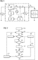
- FIG. 1 shows by way of example and in schematic form an electronic fuse SI with at least one controllable switching element SE, which is set up to carry out the method according to the invention for reducing a temperature rise in the switching element SE.
- the electronic fuse For example, SI can be switched between a supply source and an electrical load L as a protection device.
- a supply source for example, a voltage source is used, from which an input voltage U E is supplied.
- the electrical load L comprises, for example, an ohmic component R L and a capacitive component C L , which leads to relatively high inrush currents when the switching element SE of the electrical fuse SI is switched on or at the moment of switch-on.
- the electrical load can also have an inductive component, for example.
- An output voltage U A of the electrical fuse SI is applied to the load L and an output current I A of the electrical fuse SI flows into the load L, wherein a maximum permissible continuous current I L can be set for a running operation of the fuse.
- This continuous current I L may, for example, correspond to a so-called rated current for the electrical load L or may assume a predeterminable value, usually below the rated current.
- line losses, copper and line losses of the fuse SI, internal resistance of the supply source, etc. are shown as parasitic, ohmic resistance R p , by which the inrush currents or the current pulse at least slightly limited at power.
- R p parasitic, ohmic resistance
- the inrush currents or the current pulse at least slightly limited at power.
- one mounted with the switching element SE in series - in FIG. 1 not shown - impedance can be provided.
- This impedance can be designed, for example, as an ohmic resistor with a fixed or variable resistance value (eg as a thermistor).
- the electrical fuse SI may optionally have an additional protection device SV in addition to the controllable switching element SE.
- an additional protection device SV for example, a fuse can be used, which in the event of a fault (eg in the case of a short circuit, etc.) should respond, but should not be triggered when the power is turned on by the resulting current pulses or inrush currents.
- a switching element SE can in the electrical fuse, for example, a transistor - in particular a so-called metal-oxide-semiconductor field effect transistor or MOS-FET - are used. Ideally, an n-channel MOS-FET is used.
- the switching element SE is driven by a drive signal AS, which is applied as a switching element SE, for example as a so-called gate-source voltage in a MOS-FET.
- the drive signal AS also limits a maximum possible current increase di A (t) / dt of the output current I A flowing into the load L when the load L is switched on.
- the drive signal AS is generated from a default signal VS by means of a drive unit AE and is, for example - as in FIG.
- the default signal VS is determined by an evaluation unit AW on the basis of a time profile of the output current I A and / or the output voltage U A and / or a temperature of the switching element SE. That is, for the generation of the default signal VS, which also includes default values such as switch-off, duty cycle and / or switch-off for the inventive method, at least one of the time profiles of output current I A or output voltage U A or temperature of the switching element SE is used as a reference variable.
- the default signal VS can be configured as a pulse-width-modulated square-wave signal and predetermines the respective configuration of the drive signal AS (eg slope and length of the ramp shape) by taking into account the default values.
- a monitoring unit UE is provided for determining the time profiles of the output current I A and / or the output voltage U A and / or the temperature of the switching element SE. For example, measured values of output current I A and / or output voltage U A and / or temperature of switching element SE are collected by monitoring unit UE, which are determined, for example, by corresponding sensor or measuring devices T SE , A, V.
- T SE sensor or measuring devices
- the temperature of the switching element SE - as exemplified in FIG. 1 shown - directly determined directly on the switching element SE.
- the temperature of the switching element SE can also be determined indirectly on a housing of the switching element SE.
- the switching element SE can be embodied as an integrated component, wherein this integrated component can comprise at least the monitoring unit UE and the control unit AW and optionally existing sensor or measuring devices T SE , A, V for eg temperature, current and / or voltage.
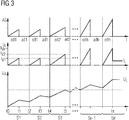
- FIG. 2 shows by way of example a preferred sequence of the method according to the invention for reducing the temperature rise in a controllable switching element SE of an electrical fuse SI as exemplified in FIG. 1 shown.
- the method begins with an initialization or calibration step 100.
- a thermal model of the switching element SE for example the so-called Cauer network or the so-called Foster network, first default values for a switch-on duration of the switching element SE and / or a switch-off current are determined and determined as start values for a switch-off duration of the switching element SE.
- the maximum permissible junction temperature can be taken into account.
- the maximum possible current increase of the output current I A and, if appropriate, a maximum permissible temperature deviation of the junction temperature can be derived. That is, in the calibration step 100, for example, from the thermal model of the switching element SE for an unfavorable combination of the ohmic components R L and the capacitive component C L of the load L, a maximum possible or permissible current increase di A (t) / dt of the output current I A or optionally determined a maximum allowable temperature of the junction temperature.
- the default signal VS - based on the first default values - is then forwarded to the drive unit AE and used to generate the first drive signal AS for the switching element SE, for example, as a ramp-shaped drive signal AS.
- a switch-on step 101 the switching element SE is controlled by the drive signal AS turned on.
- the switching element SE is controlled by the drive signal AS such that the current flowing in the load L output current I A or the corresponding current increase di A (t) / dt when turning on the load L is limited so that a time course of the junction temperature of Switching element SE does not exceed a critical value of the junction temperature or no damage to the switching element SE occurs.
- Parallel to the switching-on step 101 at least one of the time profiles of the output current I A and / or the output voltage U A and / or the temperature of the switching element SE is monitored in a measuring step 102, for example by means of sensor or measuring devices T SE , A, V, with the aid of the monitoring unit UE determined.
- Averaging of the individual ascertained time profiles of the output current I A and / or output voltage U A and / or temperature of the switching element SE can be carried out mathematically, for example by forming the respective arithmetic mean or by forming rms values, or alternatively by means of filtering (for example with Low-pass or high-pass filters of any order) or by excluding or selecting determined values from the respective time profile.
- the measuring step 102 and the determining step 103 are performed parallel to or substantially independent of other steps for carrying out the method according to the invention. However, it is checked in a default checking step 109 whether the evaluation unit AW has determined new default values for the switch-on duration and / or the switch-off current and the switch-off duration.
- a demolition test step 104 it is then checked whether a determined value of the determined, temporal course of the output voltage U A has been reached at which a predefinable difference is undershot with respect to the input voltage U E of the electronic fuse SI. That is, for example, it is checked whether a difference between the input voltage U E and the output voltage U A (eg, an average value from the ascertained time profile) falls below a predefinable tolerance value.
- the demolition check step 104 it can also be checked whether the determined, time course of the Output current I A falls below a predetermined maximum continuous current I L.
- an average value from the determined, time course of the output current I A can be used.
- the demolition test step 104 can be performed, for example, by the evaluation unit AW.
- the time profiles of output voltage U A and output current I A can be determined, for example, in measuring step 102.
- the switching element SE remains switched on until it is determined in a switching test step 106 that the default value of the switch-on duration is at least the starting value for the switch-on duration of the switching element SE, for example in the case of a first switching cycle of the switching element SE is reached.
- the switching test step 106 it is also possible to check whether the predetermined value or, in the first switching cycle of the switching element SE, the predetermined start value of the switch-off current is at least reached or exceeded by the respective output current I A currently determined in the measuring step 102.
- the switching test step 106 can be carried out, for example, by the evaluation unit AW.
- the time profile of the temperature of the switching element SE ascertained in the measuring step 102 can be compared with a predefinable limit temperature for the switching element SE.
- the predeterminable limit temperature for the switching element SE for example be derived from the thermal model of the switching element SE.
- the switch element SE is switched off in a switch-off step 107. Additionally or alternatively, reaching or exceeding the predeterminable limit temperature by the determined, temporal course of the temperature at the switching element SE for performing the Ausschalt suitss 107 and for switching off the switching element SE lead.
- the switching element SE then remains switched off until the preset value of the switch-off duration or, in the first switch cycle, the starting value or first setpoint value of the switch-off duration is at least reached or exceeded.
- the achievement of the predetermined switch-off duration is checked in a switch-off test step 108. If the predetermined switch-off duration has been reached, then it can be determined in the default checking step 109 whether new default values for the switch-on duration and / or the switch-off current and the switch-off duration in the determining step 103 are determined by the evaluation unit AW on the basis of the ascertained, temporal course of the output current I A and / or output voltage U A and / or the temperature of the switching element SE have been determined.
- the previous default values will continue to be used at least for the next switching cycle of the switching element SE or the process.
- the switching element SE is then turned on again in the turn-on step 101, wherein the default values and thus the drive signal AS remain unchanged.
- the previous default values are replaced by the new default values in an exchange step 110 and used for the default signal VS or spent with this. That is, the default signal VS is adapted, for example, by the evaluation unit AW on the basis of the new default values and converted via the control unit into a new or adapted control signal AS for the switching element SE.
- the switching element SE is then turned on in the turn-on step 101 with the adjusted drive signal AS. As a result, for example, a possible current increase di A (t) / dt be changed or regulated by the switching element SE - as exemplified in FIG. 3 shown.
- the default checking step 109 may be performed before the turn-off checking step 108. That Before the test, whether the default value of the switch-off of the switching element SE in Ausschaltprüf Republic 108 is reached, the phonessprüf intimid 109 and optionally in the presence of new default values for duty and / or switch-off and Ausschaltdauer the switching element DE, the replacement step 110 performed.
- the inventive method is then carried out until it is determined in Abbruchsprüf Colour 104 that one of the termination conditions is met, and finished with the final step 105, wherein the switching element SE remains operationally turned on.
- FIG. 3 are exemplary and schematically a time course of the drive signal AS for the switching element SE and corresponding, temporal courses of the output current I A and the output voltage U A during the course of several repetitions of the method according to the invention to a termination by the demolition test step 104 and the Final step 105 shown, wherein in a top diagram, the time profile of the drive signal AS, in a middle diagram, the time profile of the output current I A and in a lowermost diagram, the time profile of the output voltage U A are shown by way of example.
- On the respective x-axis is the time t and on the respective y-axis, the drive signal AS for the switching element SE, a corresponding curve of the output current I A and the output voltage U A applied.
- S1 through Sn cycles of the method according to the invention or S1 through Sn switching cycles are run through by the switching element SE.
- a first default value ed1 for the switch-on duration, a first default value ad1 for the switch-off duration and / or a first default value I V1 for the switch-off current are specified for the method on the basis of the thermal model of the switching element SE.
- the switching element is turned on at a first time t0 by means of the drive signal AS and thus a first switching cycle S1 is started.
- the drive signal AS can have a ramp shape for this purpose.
- a current increase di A (t) / dt of the output current I A is limited by the switching element SE - as shown by the example shown in the middle diagram, time course of the output current I A. That is, the current through the switching element SE or the output current I A increases in proportion to or regulated by the drive signal AS.
- the switch element SE is switched off by the drive signal AS 107 switched off. That is, the drive signal AS is terminated as shown in the top diagram, whereby, as shown in the middle diagram, the output current I A passes through the switching element to a value of zero.
- the output voltage U A decreases as in the bottom diagram from, since after switching off the switching element SE, the capacitive component C L of the load L - is discharged, for example, by the ohmic portion R L of the load L again.
- the temperature of the switching element SE also decreases, since during the switch-off ad1 a heat generated during the switch-on ed1 at least partially eg to the environment such as housing and subsequently to cooling devices (eg heatsink, copper surfaces, etc.) are delivered.
- a heat generated during the switch-on ed1 at least partially eg to the environment such as housing and subsequently to cooling devices (eg heatsink, copper surfaces, etc.) are delivered.
- the charging of the capacitive component C L of the load or the increase of the output voltage U A has the consequence that less energy loss is converted in the switching element SE.
- the default values for the switch-on duration and / or switch-off current and the switch-off duration can be adapted for at least one subsequent switch cycle S2 and thus the drive signal AS.
- at least one of the time profiles of output current I A and / or output voltage U A and / or temperature of the switching element SE is used and it can be calculated by the evaluation AW new default values.
- the switching element SE is turned on by the turn-on step 101 for a second switching cycle S2 at a third time t2. Since it was determined in the default test step 109 that, for example, there are still no new default values for switch-on duration and / or switch-off current and switch-off duration or have been calculated by the evaluation unit AW, the first preset values ed1, ad1, I V1 continue to be used for the second switch cycle S2. That is, as shown in the top diagram, the course of the drive signal AS in the second switching cycle S2 corresponds to the course in the first switching cycle S1.
- the switching element SE is switched off by the drive signal AS 107 again switched off - until the fifth predetermined value ad1 of the switch-off duration is reached in a fifth time t4.
- the replacement values for a third switch cycle S3 in the replacement step 110 are the new default values ed2, Ad2, I V2 adopted.
- a new default signal VS and thus a new drive signal AS - as exemplarily in the top diagram for the third switching cycle S3 - is generated.
- the switching element SE is then switched on again in the switch-on step 101 with the new drive signal AS.
- the switching element SE is in a sixth time t5 - when reaching the new default value ed2 of the duty cycle or when reaching the new default value I V2 of the breaking current in the switching step 107 off again until the new default ad2 of the off period is reached.
- the method is run through until, for example, in an nth switching cycle of the switching element SE at a time tn in the demolition test step 104, it is determined that a value has been reached from the determined, temporal profile of the output voltage U A , with respect to the input voltage U E the electronic fuse SI a predetermined difference is exceeded. This means that an output voltage U A or U L sets in which approximates the input voltage U E the electrical fuse SI corresponds.
- the demolition test step 104 it can also be checked whether a predefinable, maximum continuous current I L is reached or undershot, respectively, from the determined, temporal course of the output current I A.
- the self-adjusting output current I A or I L corresponds to the self-adjusting output voltage U L divided by the ohmic component R L of the load.
- the capacitive component C L of the load L is fully charged at time tn. Either a value is reached by the time curve of the output voltage U A , in which with respect to the input voltage U E of the electronic fuse SI a predetermined difference is exceeded, or from the time course of the output current I A reaches a predetermined maximum continuous current I L or undershoot, the inventive method is terminated or terminated in a final step 105 and the switching element SE remains switched on for ongoing operation.
Landscapes
- Engineering & Computer Science (AREA)
- Power Engineering (AREA)
- Electronic Switches (AREA)
- Power Conversion In General (AREA)
- Dc-Dc Converters (AREA)
Priority Applications (6)
| Application Number | Priority Date | Filing Date | Title |
|---|---|---|---|
| EP18169794.7A EP3561981A1 (fr) | 2018-04-27 | 2018-04-27 | Procédé de réduction de montée en température dans un élément de commutation recommandable |
| CN201980043097.5A CN112292793B (zh) | 2018-04-27 | 2019-03-29 | 用于减小可控开关元件的热载荷的方法 |
| EP19716825.5A EP3776783A1 (fr) | 2018-04-27 | 2019-03-29 | Procédé de réduction d'une contrainte thermique d'un élément de commutation commandable |
| US17/050,644 US11349472B2 (en) | 2018-04-27 | 2019-03-29 | Method for reducing a thermal load on a controllable switching element |
| PCT/EP2019/058037 WO2019206564A1 (fr) | 2018-04-27 | 2019-03-29 | Procédé de réduction d'une contrainte thermique d'un élément de commutation commandable |
| PCT/EP2019/060466 WO2019206964A1 (fr) | 2018-04-27 | 2019-04-24 | Procédé de réduction d'une élévation de température dans un élément de commutation commandable |
Applications Claiming Priority (1)
| Application Number | Priority Date | Filing Date | Title |
|---|---|---|---|
| EP18169794.7A EP3561981A1 (fr) | 2018-04-27 | 2018-04-27 | Procédé de réduction de montée en température dans un élément de commutation recommandable |
Publications (1)
| Publication Number | Publication Date |
|---|---|
| EP3561981A1 true EP3561981A1 (fr) | 2019-10-30 |
Family
ID=62089611
Family Applications (2)
| Application Number | Title | Priority Date | Filing Date |
|---|---|---|---|
| EP18169794.7A Withdrawn EP3561981A1 (fr) | 2018-04-27 | 2018-04-27 | Procédé de réduction de montée en température dans un élément de commutation recommandable |
| EP19716825.5A Pending EP3776783A1 (fr) | 2018-04-27 | 2019-03-29 | Procédé de réduction d'une contrainte thermique d'un élément de commutation commandable |
Family Applications After (1)
| Application Number | Title | Priority Date | Filing Date |
|---|---|---|---|
| EP19716825.5A Pending EP3776783A1 (fr) | 2018-04-27 | 2019-03-29 | Procédé de réduction d'une contrainte thermique d'un élément de commutation commandable |
Country Status (4)
| Country | Link |
|---|---|
| US (1) | US11349472B2 (fr) |
| EP (2) | EP3561981A1 (fr) |
| CN (1) | CN112292793B (fr) |
| WO (2) | WO2019206564A1 (fr) |
Cited By (1)
| Publication number | Priority date | Publication date | Assignee | Title |
|---|---|---|---|---|
| DE102022130544A1 (de) | 2022-11-18 | 2024-05-23 | Bayerische Motoren Werke Aktiengesellschaft | Thermisch lebensdaueroptimierte leistungselektronische Einrichtung, Betriebsverfahren und Kraftfahrzeug |
Families Citing this family (12)
| Publication number | Priority date | Publication date | Assignee | Title |
|---|---|---|---|---|
| DE102020116424A1 (de) * | 2020-06-22 | 2021-12-23 | Bayerische Motoren Werke Aktiengesellschaft | Verfahren und elektronische Einrichtung zur Temperaturüberwachung einer Leistungselektronik und Kraftfahrzeug |
| EP4009063A1 (fr) * | 2020-12-01 | 2022-06-08 | Siemens Aktiengesellschaft | Module de sortie et procédé de fonctionnement |
| US12136913B2 (en) | 2021-06-18 | 2024-11-05 | Aptiv Technologies AG | Solid-state multi-channel protection circuit |
| DE102022129958A1 (de) * | 2021-11-18 | 2023-05-25 | Elmos Semiconductor Se | Elektronische Sicherung mit Übermittlung spezieller Daten |
| US11870428B1 (en) * | 2022-08-26 | 2024-01-09 | Infineon Technologies Austria Ag | System and method for pulsed gate control of a transistor |
| US12122251B2 (en) | 2022-09-28 | 2024-10-22 | BorgWarner US Technologies LLC | Systems and methods for bidirectional message architecture for inverter for electric vehicle |
| WO2024069457A1 (fr) * | 2022-09-28 | 2024-04-04 | Delphi Technologies Ip Limited | Systèmes et procédés de décharge active contrôlée pour onduleur pour véhicule électrique |
| DE102024100121B4 (de) * | 2024-01-03 | 2026-08-20 | Infineon Technologies Ag | Intelligenter elektronischer schalter |
| DE102024200963A1 (de) * | 2024-02-02 | 2025-08-07 | Ellenberger & Poensgen Gmbh | Verfahren zum Betrieb eines Schutzschalters und Schutzschalter |
| EP4730652A1 (fr) * | 2024-10-21 | 2026-04-22 | Aptiv Technologies AG | Procédé de charge capacitive |
| EP4734310A1 (fr) * | 2024-10-24 | 2026-04-29 | Aptiv Technologies AG | Circuit d'entrée d'alimentation pour gérer des courants d'appel |
| US20260163353A1 (en) * | 2024-12-09 | 2026-06-11 | Semiconductor Components Industries, Llc | Simplified thermal model for electronic fuse |
Citations (8)
| Publication number | Priority date | Publication date | Assignee | Title |
|---|---|---|---|---|
| US6225797B1 (en) | 1999-12-30 | 2001-05-01 | Lockheed Martin Corporation | Circuit for limiting inrush current through a transistor |
| EP1236257A2 (fr) | 1999-12-01 | 2002-09-04 | Siemens AG Österreich | Unite de surveillance pour alimentations electriques |
| US6552889B1 (en) * | 2001-07-17 | 2003-04-22 | Vishay Siliconix | Current limiting technique for hybrid power MOSFET circuits |
| DE20302275U1 (de) | 2002-02-14 | 2003-06-05 | Ellenberger & Poensgen GmbH, 90518 Altdorf | Elektronischer Schalter |
| EP1384303A2 (fr) | 2001-04-06 | 2004-01-28 | Siemens AG Österreich | Alimentation en courant avec securite coupe-circuit |
| WO2011107314A1 (fr) * | 2010-03-02 | 2011-09-09 | Siemens Aktiengesellschaft | Coupe-circuit électronique |
| DE102012103551A1 (de) | 2012-04-23 | 2013-10-24 | Block Transformatoren-Elektronik Gmbh | Elektronische Sicherungsvorrichtung und elektronisches Sicherungsverfahren |
| US20150303917A1 (en) * | 2014-04-18 | 2015-10-22 | International Business Machines Corporation | Controlling turn on fets of a hot plug device |
Family Cites Families (21)
| Publication number | Priority date | Publication date | Assignee | Title |
|---|---|---|---|---|
| US6281669B1 (en) * | 1997-09-02 | 2001-08-28 | Siemens Aktiengesellschaft | Circuit arrangement and method for limiting current for consumers of alternating current |
| US6347028B1 (en) * | 1999-06-21 | 2002-02-12 | Lutron Electronics Co., Inc. | Load control system having an overload protection circuit |
| US7064946B2 (en) * | 2003-12-18 | 2006-06-20 | International Rectifier Corporation | Electronic fuse |
| US20060028257A1 (en) * | 2004-08-03 | 2006-02-09 | Hong Huang | System and method for over-temperature protection sensing employing MOSFET on-resistance Rds_on |
| JP4995647B2 (ja) * | 2007-06-12 | 2012-08-08 | 矢崎総業株式会社 | 過熱保護機能付き半導体装置の制御回路 |
| US8582263B2 (en) * | 2009-10-20 | 2013-11-12 | Intrinsic Audio Solutions, Inc. | Digitally controlled AC protection and attenuation circuit |
| DE102009060346A1 (de) * | 2009-12-24 | 2011-06-30 | Merten GmbH & Co. KG, 51674 | Elektrische Schaltung zum Schalten und/oder Dimmen von Lasten |
| KR101541632B1 (ko) * | 2011-01-14 | 2015-08-03 | 파나소닉 주식회사 | 반도체 스위치 소자의 구동 장치 |
| EP2676369A1 (fr) * | 2011-02-18 | 2013-12-25 | Freescale Semiconductor, Inc. | Dispositif de protection contre les surcharges et procédé de fonctionnement d'un commutateur d'alimentation |
| FR2985115B1 (fr) * | 2011-12-21 | 2014-03-07 | Continental Automotive France | Commande d'une charge inductive avec mecanisme de reduction de courant sensible a la temperature |
| ITMI20130001A1 (it) * | 2013-01-03 | 2014-07-04 | St Microelectronics Srl | SISTEMA ELETTRICO COMPRENDENTE UN APPARATO DI PILOTAGGIO DI UN CARICO CON AUTO-RIAVVIO E METODO DI FUNZIONAMENTO DELLÂeuro¿APPARATO |
| CN108736867B (zh) * | 2013-11-14 | 2022-03-18 | 三菱电机株式会社 | 半导体开关元件的驱动电路 |
| DE202014011366U1 (de) * | 2014-08-28 | 2019-10-18 | Ellenberger & Poensgen Gmbh | Elektronischer Schutzschalter |
| JP6291432B2 (ja) * | 2015-02-04 | 2018-03-14 | 矢崎総業株式会社 | 突入電流抑制回路 |
| DE102015114460B4 (de) | 2015-08-31 | 2022-06-09 | Infineon Technologies Ag | Versorgungslast mit Einschaltstromverhalten |
| DE102015121194A1 (de) * | 2015-12-04 | 2017-06-08 | Infineon Technologies Ag | Vorrichtung mit integriertem Schutzverlauf und Verfahren |
| US10965120B2 (en) * | 2016-04-08 | 2021-03-30 | Infineon Technologies Ag | Electronic switching and protection circuit with test mode function |
| US11404866B2 (en) * | 2016-04-08 | 2022-08-02 | Infineon Technologies Ag | Electronic switching and protection circuit with several operation modes |
| US10170905B2 (en) * | 2016-04-08 | 2019-01-01 | Infineon Technologies Ag | Electronic switching and protection circuit with wakeup function |
| CN107749713B (zh) * | 2017-10-16 | 2020-01-21 | 成都芯源系统有限公司 | 负载响应改善单元、开关型功率变换器及其控制方法 |
| DE102019125122A1 (de) * | 2019-09-18 | 2021-03-18 | Infineon Technologies Ag | Intelligenter elektronischer schalter |
-
2018
- 2018-04-27 EP EP18169794.7A patent/EP3561981A1/fr not_active Withdrawn
-
2019
- 2019-03-29 WO PCT/EP2019/058037 patent/WO2019206564A1/fr not_active Ceased
- 2019-03-29 EP EP19716825.5A patent/EP3776783A1/fr active Pending
- 2019-03-29 CN CN201980043097.5A patent/CN112292793B/zh active Active
- 2019-03-29 US US17/050,644 patent/US11349472B2/en active Active
- 2019-04-24 WO PCT/EP2019/060466 patent/WO2019206964A1/fr not_active Ceased
Patent Citations (8)
| Publication number | Priority date | Publication date | Assignee | Title |
|---|---|---|---|---|
| EP1236257A2 (fr) | 1999-12-01 | 2002-09-04 | Siemens AG Österreich | Unite de surveillance pour alimentations electriques |
| US6225797B1 (en) | 1999-12-30 | 2001-05-01 | Lockheed Martin Corporation | Circuit for limiting inrush current through a transistor |
| EP1384303A2 (fr) | 2001-04-06 | 2004-01-28 | Siemens AG Österreich | Alimentation en courant avec securite coupe-circuit |
| US6552889B1 (en) * | 2001-07-17 | 2003-04-22 | Vishay Siliconix | Current limiting technique for hybrid power MOSFET circuits |
| DE20302275U1 (de) | 2002-02-14 | 2003-06-05 | Ellenberger & Poensgen GmbH, 90518 Altdorf | Elektronischer Schalter |
| WO2011107314A1 (fr) * | 2010-03-02 | 2011-09-09 | Siemens Aktiengesellschaft | Coupe-circuit électronique |
| DE102012103551A1 (de) | 2012-04-23 | 2013-10-24 | Block Transformatoren-Elektronik Gmbh | Elektronische Sicherungsvorrichtung und elektronisches Sicherungsverfahren |
| US20150303917A1 (en) * | 2014-04-18 | 2015-10-22 | International Business Machines Corporation | Controlling turn on fets of a hot plug device |
Cited By (2)
| Publication number | Priority date | Publication date | Assignee | Title |
|---|---|---|---|---|
| DE102022130544A1 (de) | 2022-11-18 | 2024-05-23 | Bayerische Motoren Werke Aktiengesellschaft | Thermisch lebensdaueroptimierte leistungselektronische Einrichtung, Betriebsverfahren und Kraftfahrzeug |
| WO2024104715A1 (fr) | 2022-11-18 | 2024-05-23 | Bayerische Motoren Werke Aktiengesellschaft | Dispositif électronique de puissance à durée de vie optimisée thermiquement, procédé de fonctionnement et véhicule à moteur |
Also Published As
| Publication number | Publication date |
|---|---|
| US20210044288A1 (en) | 2021-02-11 |
| WO2019206964A1 (fr) | 2019-10-31 |
| CN112292793A (zh) | 2021-01-29 |
| CN112292793B (zh) | 2022-12-13 |
| EP3776783A1 (fr) | 2021-02-17 |
| US11349472B2 (en) | 2022-05-31 |
| WO2019206564A1 (fr) | 2019-10-31 |
Similar Documents
| Publication | Publication Date | Title |
|---|---|---|
| WO2019206964A1 (fr) | Procédé de réduction d'une élévation de température dans un élément de commutation commandable | |
| EP3224631B1 (fr) | Procédé de détermination d'un vieillissement de modules semi-conducteurs de puissance, dispositif et circuit | |
| DE60005186T2 (de) | Last-steuerungssystem mit einer überlast-schutzschaltung | |
| EP3078105B1 (fr) | Système d'alimentation électrique et procédé de limitation du courant de sortie d'un système d'alimentation électrique | |
| DE112013007331B4 (de) | Motorsteuerungsvorrichtung | |
| EP2562896A2 (fr) | Circuit de commande destiné à limiter un courant de charge, commutation de charge et véhicule automobile | |
| DE102014200946B4 (de) | Überlast-Überwachungsvorrichtung und Verfahren zur Überlast-Überwachung | |
| DE102017107520A1 (de) | Elektronische Schalt- und Schutzschaltung mit einem logarithmischen ADC | |
| DE102017107522A1 (de) | Elektronische Schalt- und Schutzschaltung mit Testbetriebsfunktion | |
| DE102009003206A1 (de) | Vorrichtung zum Detektieren eines Betriebszustands eines Leistungshalbleiterbauelements | |
| DE102020125642B4 (de) | System, Verfahren und Computerprogrammprodukt zur Überwachung der Kühlleistung für einen Halbleiter-Pulswechselrichter | |
| DE102014202717B3 (de) | System zur Kapazitätsbestimmung eines Zwischenkreiskondensators und Verfahren zum Ansteuern eines Wechselrichters | |
| DE10351843A1 (de) | Verfahren und elektrische Schaltungen zur Ermittlung einer Temperatur eines Leistungshalbleiters | |
| DE102020203123A1 (de) | Verfahren und Vorrichtung zur Bestimmung der Schaltverlustleistung | |
| EP3281266A1 (fr) | Procédé et dispositif pour l'alimentation en énergie d'une charge à basse tension | |
| DE102014012828A1 (de) | Elektronischer Schutzschalter | |
| DE102020116424A1 (de) | Verfahren und elektronische Einrichtung zur Temperaturüberwachung einer Leistungselektronik und Kraftfahrzeug | |
| DE102016207014A1 (de) | Elektronische Sicherung für ein Fahrzeug | |
| EP4012926B1 (fr) | Commutateur à courant continu | |
| DE102007018829A1 (de) | Verfahren und Vorrichtung zur Ansteuerung einer Leistungsschaltereinheit | |
| EP3364512B1 (fr) | Procédé et dispositif de protection d'un moteur électrique contre la surchauffe | |
| DE102013208326B4 (de) | Verfahren zum Betreiben eines Wechselrichters, Wechselrichter | |
| DE3539646C2 (de) | Schaltungsanordnung zum Schutz gegen Überlast | |
| EP3895312B1 (fr) | Commutateur électronique à régulation du courant | |
| EP2639949A1 (fr) | Alimentation en courant avec circuit intermédiaire |
Legal Events
| Date | Code | Title | Description |
|---|---|---|---|
| PUAI | Public reference made under article 153(3) epc to a published international application that has entered the european phase |
Free format text: ORIGINAL CODE: 0009012 |
|
| STAA | Information on the status of an ep patent application or granted ep patent |
Free format text: STATUS: THE APPLICATION HAS BEEN PUBLISHED |
|
| AK | Designated contracting states |
Kind code of ref document: A1 Designated state(s): AL AT BE BG CH CY CZ DE DK EE ES FI FR GB GR HR HU IE IS IT LI LT LU LV MC MK MT NL NO PL PT RO RS SE SI SK SM TR |
|
| AX | Request for extension of the european patent |
Extension state: BA ME |
|
| STAA | Information on the status of an ep patent application or granted ep patent |
Free format text: STATUS: THE APPLICATION IS DEEMED TO BE WITHDRAWN |
|
| 18D | Application deemed to be withdrawn |
Effective date: 20200603 |