EP3563418B1 - Dispositif optoélectronique à diodes électroluminescentes - Google Patents
Dispositif optoélectronique à diodes électroluminescentes Download PDFInfo
- Publication number
- EP3563418B1 EP3563418B1 EP17822341.8A EP17822341A EP3563418B1 EP 3563418 B1 EP3563418 B1 EP 3563418B1 EP 17822341 A EP17822341 A EP 17822341A EP 3563418 B1 EP3563418 B1 EP 3563418B1
- Authority
- EP
- European Patent Office
- Prior art keywords
- light
- photoluminescent
- radiation
- wavelength
- optoelectronic device
- Prior art date
- Legal status (The legal status is an assumption and is not a legal conclusion. Google has not performed a legal analysis and makes no representation as to the accuracy of the status listed.)
- Active
Links
Images



Classifications
-
- F—MECHANICAL ENGINEERING; LIGHTING; HEATING; WEAPONS; BLASTING
- F21—LIGHTING
- F21K—NON-ELECTRIC LIGHT SOURCES USING LUMINESCENCE; LIGHT SOURCES USING ELECTROCHEMILUMINESCENCE; LIGHT SOURCES USING CHARGES OF COMBUSTIBLE MATERIAL; LIGHT SOURCES USING SEMICONDUCTOR DEVICES AS LIGHT-GENERATING ELEMENTS; LIGHT SOURCES NOT OTHERWISE PROVIDED FOR
- F21K9/00—Light sources using semiconductor devices as light-generating elements, e.g. using light-emitting diodes [LED] or lasers
- F21K9/60—Optical arrangements integrated in the light source, e.g. for improving the colour rendering index or the light extraction
- F21K9/64—Optical arrangements integrated in the light source, e.g. for improving the colour rendering index or the light extraction using wavelength conversion means distinct or spaced from the light-generating element, e.g. a remote phosphor layer
-
- H—ELECTRICITY
- H10—SEMICONDUCTOR DEVICES; ELECTRIC SOLID-STATE DEVICES NOT OTHERWISE PROVIDED FOR
- H10H—INORGANIC LIGHT-EMITTING SEMICONDUCTOR DEVICES HAVING POTENTIAL BARRIERS
- H10H29/00—Integrated devices, or assemblies of multiple devices, comprising at least one light-emitting semiconductor element covered by group H10H20/00
- H10H29/10—Integrated devices comprising at least one light-emitting semiconductor component covered by group H10H20/00
- H10H29/14—Integrated devices comprising at least one light-emitting semiconductor component covered by group H10H20/00 comprising multiple light-emitting semiconductor components
- H10H29/142—Two-dimensional arrangements, e.g. asymmetric LED layout
-
- F—MECHANICAL ENGINEERING; LIGHTING; HEATING; WEAPONS; BLASTING
- F21—LIGHTING
- F21K—NON-ELECTRIC LIGHT SOURCES USING LUMINESCENCE; LIGHT SOURCES USING ELECTROCHEMILUMINESCENCE; LIGHT SOURCES USING CHARGES OF COMBUSTIBLE MATERIAL; LIGHT SOURCES USING SEMICONDUCTOR DEVICES AS LIGHT-GENERATING ELEMENTS; LIGHT SOURCES NOT OTHERWISE PROVIDED FOR
- F21K9/00—Light sources using semiconductor devices as light-generating elements, e.g. using light-emitting diodes [LED] or lasers
- F21K9/60—Optical arrangements integrated in the light source, e.g. for improving the colour rendering index or the light extraction
- F21K9/68—Details of reflectors forming part of the light source
-
- F—MECHANICAL ENGINEERING; LIGHTING; HEATING; WEAPONS; BLASTING
- F21—LIGHTING
- F21K—NON-ELECTRIC LIGHT SOURCES USING LUMINESCENCE; LIGHT SOURCES USING ELECTROCHEMILUMINESCENCE; LIGHT SOURCES USING CHARGES OF COMBUSTIBLE MATERIAL; LIGHT SOURCES USING SEMICONDUCTOR DEVICES AS LIGHT-GENERATING ELEMENTS; LIGHT SOURCES NOT OTHERWISE PROVIDED FOR
- F21K9/00—Light sources using semiconductor devices as light-generating elements, e.g. using light-emitting diodes [LED] or lasers
- F21K9/90—Methods of manufacture
-
- F—MECHANICAL ENGINEERING; LIGHTING; HEATING; WEAPONS; BLASTING
- F21—LIGHTING
- F21V—FUNCTIONAL FEATURES OR DETAILS OF LIGHTING DEVICES OR SYSTEMS THEREOF; STRUCTURAL COMBINATIONS OF LIGHTING DEVICES WITH OTHER ARTICLES, NOT OTHERWISE PROVIDED FOR
- F21V13/00—Producing particular characteristics or distribution of the light emitted by means of a combination of elements specified in two or more of main groups F21V1/00 - F21V11/00
- F21V13/12—Combinations of only three kinds of elements
- F21V13/14—Combinations of only three kinds of elements the elements being filters or photoluminescent elements, reflectors and refractors
-
- H—ELECTRICITY
- H10—SEMICONDUCTOR DEVICES; ELECTRIC SOLID-STATE DEVICES NOT OTHERWISE PROVIDED FOR
- H10H—INORGANIC LIGHT-EMITTING SEMICONDUCTOR DEVICES HAVING POTENTIAL BARRIERS
- H10H20/00—Individual inorganic light-emitting semiconductor devices having potential barriers, e.g. light-emitting diodes [LED]
- H10H20/80—Constructional details
- H10H20/81—Bodies
- H10H20/822—Materials of the light-emitting regions
- H10H20/824—Materials of the light-emitting regions comprising only Group III-V materials, e.g. GaP
- H10H20/825—Materials of the light-emitting regions comprising only Group III-V materials, e.g. GaP containing nitrogen, e.g. GaN
-
- H—ELECTRICITY
- H10—SEMICONDUCTOR DEVICES; ELECTRIC SOLID-STATE DEVICES NOT OTHERWISE PROVIDED FOR
- H10H—INORGANIC LIGHT-EMITTING SEMICONDUCTOR DEVICES HAVING POTENTIAL BARRIERS
- H10H20/00—Individual inorganic light-emitting semiconductor devices having potential barriers, e.g. light-emitting diodes [LED]
- H10H20/80—Constructional details
- H10H20/85—Packages
- H10H20/8506—Containers
-
- H—ELECTRICITY
- H10—SEMICONDUCTOR DEVICES; ELECTRIC SOLID-STATE DEVICES NOT OTHERWISE PROVIDED FOR
- H10W—GENERIC PACKAGES, INTERCONNECTIONS, CONNECTORS OR OTHER CONSTRUCTIONAL DETAILS OF DEVICES COVERED BY CLASS H10
- H10W90/00—Package configurations
-
- F—MECHANICAL ENGINEERING; LIGHTING; HEATING; WEAPONS; BLASTING
- F21—LIGHTING
- F21Y—INDEXING SCHEME ASSOCIATED WITH SUBCLASSES F21K, F21L, F21S and F21V, RELATING TO THE FORM OR THE KIND OF THE LIGHT SOURCES OR OF THE COLOUR OF THE LIGHT EMITTED
- F21Y2105/00—Planar light sources
- F21Y2105/10—Planar light sources comprising a two-dimensional [2D] array of point-like light-generating elements
- F21Y2105/14—Planar light sources comprising a two-dimensional [2D] array of point-like light-generating elements characterised by the overall shape of the two-dimensional [2D] array
- F21Y2105/16—Planar light sources comprising a two-dimensional [2D] array of point-like light-generating elements characterised by the overall shape of the two-dimensional [2D] array square or rectangular, e.g. for light panels
-
- F—MECHANICAL ENGINEERING; LIGHTING; HEATING; WEAPONS; BLASTING
- F21—LIGHTING
- F21Y—INDEXING SCHEME ASSOCIATED WITH SUBCLASSES F21K, F21L, F21S and F21V, RELATING TO THE FORM OR THE KIND OF THE LIGHT SOURCES OR OF THE COLOUR OF THE LIGHT EMITTED
- F21Y2115/00—Light-generating elements of semiconductor light sources
- F21Y2115/10—Light-emitting diodes [LED]
-
- F—MECHANICAL ENGINEERING; LIGHTING; HEATING; WEAPONS; BLASTING
- F21—LIGHTING
- F21Y—INDEXING SCHEME ASSOCIATED WITH SUBCLASSES F21K, F21L, F21S and F21V, RELATING TO THE FORM OR THE KIND OF THE LIGHT SOURCES OR OF THE COLOUR OF THE LIGHT EMITTED
- F21Y2115/00—Light-generating elements of semiconductor light sources
- F21Y2115/30—Semiconductor lasers
-
- H—ELECTRICITY
- H10—SEMICONDUCTOR DEVICES; ELECTRIC SOLID-STATE DEVICES NOT OTHERWISE PROVIDED FOR
- H10H—INORGANIC LIGHT-EMITTING SEMICONDUCTOR DEVICES HAVING POTENTIAL BARRIERS
- H10H20/00—Individual inorganic light-emitting semiconductor devices having potential barriers, e.g. light-emitting diodes [LED]
- H10H20/01—Manufacture or treatment
- H10H20/036—Manufacture or treatment of packages
- H10H20/0361—Manufacture or treatment of packages of wavelength conversion means
-
- H—ELECTRICITY
- H10—SEMICONDUCTOR DEVICES; ELECTRIC SOLID-STATE DEVICES NOT OTHERWISE PROVIDED FOR
- H10H—INORGANIC LIGHT-EMITTING SEMICONDUCTOR DEVICES HAVING POTENTIAL BARRIERS
- H10H20/00—Individual inorganic light-emitting semiconductor devices having potential barriers, e.g. light-emitting diodes [LED]
- H10H20/80—Constructional details
- H10H20/85—Packages
- H10H20/851—Wavelength conversion means
- H10H20/8511—Wavelength conversion means characterised by their material, e.g. binder
- H10H20/8512—Wavelength conversion materials
-
- H—ELECTRICITY
- H10—SEMICONDUCTOR DEVICES; ELECTRIC SOLID-STATE DEVICES NOT OTHERWISE PROVIDED FOR
- H10H—INORGANIC LIGHT-EMITTING SEMICONDUCTOR DEVICES HAVING POTENTIAL BARRIERS
- H10H20/00—Individual inorganic light-emitting semiconductor devices having potential barriers, e.g. light-emitting diodes [LED]
- H10H20/80—Constructional details
- H10H20/85—Packages
- H10H20/851—Wavelength conversion means
- H10H20/8514—Wavelength conversion means characterised by their shape, e.g. plate or foil
Definitions
- the present disclosure relates to an optoelectronic device, particularly a display screen or an image projection device, with light-emitting components, particularly light-emitting diodes, based on semiconductor materials and their manufacturing methods.
- a pixel of an image corresponds to the unit element of the image displayed by the optoelectronic device.
- the optoelectronic device is a color image display optoelectronic device, it generally comprises for the display of each pixel of the image at least three components, also called display sub-pixels, which each emit a light radiation substantially in a single color (for example, red, green, and blue).
- the superposing of the radiations emitted by the three display sub-pixels provides the observer with the color sensation corresponding to the pixel of the displayed image.
- the assembly formed by the three sub-display pixels used to display a pixel of an image is called display pixel of the optoelectronic device.
- each diode comprising a stack of semiconductor layers for example comprising at least one group-III element and one group-V element, called III-V compound hereafter, particularly gallium nitride (GaN).
- III-V compound particularly gallium nitride (GaN).
- known light-emitting diodes comprising a stack of semiconductor layers, for example comprising a III-V compound, and emitting a red light show poor internal quantum efficiency (IQE) for conventional III-N based structures.
- IQE internal quantum efficiency
- Blocks of photoluminescent materials may be formed on at least some of the light-emitting diodes. Each photoluminescent block is adapted to convert the radiation emitted by the associated light-emitting diode into a desired radiation.
- Known photoluminescent blocks comprise micrometer-range photoluminescent particles or quantum dots. However, known materials used to form micrometer-range photoluminescent particles show poor internal quantum efficiency. Moreover, quantum dots show reduced lifetime.
- Document EP 3 024 030 discloses an optoelectronic device with light-emitting diodes and photoluminescent blocks.
- An object of an embodiment aims at overcoming all or part of the disadvantages of the previously-described optoelectronic devices comprising light-emitting diodes.
- Another object of an embodiment is that the internal quantum efficiency of the photoluminescent blocks is increased.
- Another object of an embodiment is that the lifetime of the photoluminescent blocks is increased.
- the light-emitting diodes comprise a stack of semiconductor layers, for example mainly comprising a III-V compound.
- Another object of an embodiment is that all the light-emitting diodes of the optoelectronic device show high internal quantum efficiency.
- Another object of an embodiment is that the photoluminescent blocks of the optoelectronic device show high internal quantum efficiency.
- active area of a light-emitting diode designates the region of the light-emitting diode from which most of the electromagnetic radiation provided by the light-emitting diode is emitted.
- microwire designates a three-dimensional structure of elongated shape along a preferred direction, having at least two dimensions, called minor dimensions, in the range from 5 nm to 2.5 ⁇ m, preferably from 50 nm to 2.5 um, the third dimension, called major dimension, being greater than or equal to 1 time, preferably greater than or equal to 5 times, and more preferably still greater than or equal to 10 times, the largest minor dimension.
- the minor dimensions may be smaller than or equal to approximately 1 ⁇ m, preferably in the range from 100 nm to 1 ⁇ m, more preferably from 100 nm to 800 nm.
- the height of each microwire or nanowire may be greater than or equal to 500 nm, preferably in the range from 1 um to 50 um.
- the cross-section of the wires may have different shapes, such as, for example, an oval, circular, or polygonal shape, particularly triangular, rectangular, square, or hexagonal. It should thus be understood that term "diameter” mentioned in relation with a cross-section of a wire or of a layer deposited on this wire designates a quantity associated with the surface area of the targeted structure in this cross-section, corresponding, for example, to the diameter of the disk having the same surface area as the wire cross-section.
- wire is used to mean “microwire or nanowire”.
- the median line of the wire which runs through the centers of gravity of the cross-sections, in planes perpendicular to the preferred direction of the wire is substantially rectilinear and is called “axis" of the wire hereafter.
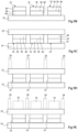
- Figures 1 and 2 show an embodiment according to the present invention of an optoelectronic device 10, for example corresponding to a display screen or to an image projection device.
- Device 10 comprises two integrated circuits 12, 14.
- First integrated circuit 12 comprises light-emitting components 16, for example light-emitting diodes, and is called optoelectronic circuit or optoelectronic chip in the following description.
- Second integrated circuit 14 comprises electronic components, not shown, especially transistors, used to control light-emitting diodes 16 of first integrated circuit 12.
- Second integrated circuit 14 is called control circuit or control chip in the following description.
- Optoelectronic circuit 12 is bonded to control circuit 14. According to the bonding type, bounding pads, not shown, may be present between optoelectronic chip 12 and control chip 14.
- a light-emitting component 16 is provided for each display subpixel Pix of electronic device 10.
- Each light-emitting components 16 comprises two opposite faces 18, 20, faces 20 of light-emitting components 16 being bounded to control circuit 14.
- Preferably all light-emitting components 16 have the same structure.
- Optoelectronic circuit 12 also comprises a substrate 22 covering light-emitting components 16 on the opposite side to control circuit 14.
- Substrate 22 has opposite faces 24, 26, face 24 being in contact with light-emitting components 16.
- Optoelectronic circuit 12 also comprises walls 28 on substrate 22. Walls 28 delimit openings 30 that expose parts of face 26.
- each opening 30 is opposite to a light-emitting component 16.
- walls 28 form a grid and openings 30 are arranged in rows and columns.
- nine subpixels Pix are shown in Figure 2 . Openings 30 have a square shape in Figure 2 . However, the shape of openings 30 may be different.
- Optoelectronic circuit 12 also comprises photoluminescent blocks 32 which are located in at least some of the openings 30, preferably in contact with face 26. Preferably, there is a photoluminescent block 32 in each opening 30. Each photoluminescent block 32 comprises a stack of semiconductor layers.
- optoelectronic circuit 12 comprises at least three types of photoluminescent blocks 32. For each pixel of the image to be displayed, optoelectronic circuit 12 comprises subpixels with photoluminescent blocks 32 of the three types. Photoluminescent blocks 32 of the first type are adapted to convert the radiation at the first wavelength into a radiation at a second wavelength by optical pumping. Photoluminescent blocks 32 of the second type are adapted to convert the radiation at the first wavelength into a radiation at a third wavelength by optical pumping. Photoluminescent blocks 32 of the third type are adapted to convert the radiation at the first wavelength into a radiation at a fourth wavelength by optical pumping.
- first, second, third and fourth wavelengths are different.
- the first wavelength corresponds to ultraviolet radiation, and is in the range from 350 nm to 430 nm.
- the second wavelength corresponds to blue light and is in the range from 440 nm to 490 nm.
- the third wavelength corresponds to green light and is in the range from 510 nm to 570 nm.
- the fourth wavelength corresponds to red light and is in a range from 600 nm to 720 nm.
- optoelectronic circuit 12 comprises photoluminescent blocks 32 of a fourth type.
- Photoluminescent blocks 32 of the fourth type are adapted to convert the radiation at the first wavelength into a radiation at a fifth wavelength by optical pumping.
- fifth wavelength corresponds to yellow light and is in a range from 570 nm to 600 nm.
- first, second, third, fourth and fifth wavelengths are different.
- optoelectronic circuit 12 comprises subpixels with photoluminescent blocks 32 of the four types.
- Optoelectronic circuit 12 also comprises a filter 33 which rests on walls 28.
- Filter 33 is adapted to block the radiation emitted from light-emitting components 16 and which has not been converted by photoluminescent blocks 32.
- Filter 33 is adapted to give way to the radiations emitted by photoluminescent blocks 32.
- the full sheet filter is non-patterned for ease of device fabrication, thus reducing manufacturing cost.
- a filling material may be present in openings 30 between walls 28, photoluminescent blocks 32 and filter 33.
- substrate 22 is made of an electrically conductive material and each light-emitting diode 16 comprises an electrically conductive element 42 running along the lateral side of light-emitting diode 16 and in contact with control circuit 14 and with substrate 22.
- Conductive element 42 is electrically insulated from light-emitting diode 16 by an electrically insulating layer 44.
- conductive elements 42 and insulating layers 44 may not be present.
- Figure 3 shows an embodiment of light-emitting diode 16 formed by a stack 35 of semiconductor layers.
- Stack 35 comprises, from bottom to top in Figure 4 :
- Figure 4 shows another embodiment of light-emitting diode 16 comprising all the elements shown in Figure 3 with the difference that substrate 20 comprises a doped semiconductor layer 40' of the second conductivity type delimiting face 24.
- Semiconductor layer 40' is made of the same material as semiconductor layers 40 of light-emitting diodes 16 and forms a structurally continuous medium with semiconductor layers 40. Semiconductor layer 40' improves current spreading into semiconductor layers 40 of light-emitting diodes 16.
- FIG. 5 shows an embodiment, that is not according to the invention and are present for illustration purposes only, of photoluminescent block 32 formed by a stack of semiconductor layers.
- Photoluminescent block 32 can be formed on substrate 22 by means of bonding via an optically transparent medium.
- Photoluminescent block 32 may comprise confinement means.
- Photoluminescent block 32 may comprise a single quantum well or multiple quantum wells.
- Photoluminescent block 32 may also comprise a buffer layer or a substrate in order to provide mechanical support to the structure.
- photoluminescent block 32 comprises a single quantum well, it may comprise an active semiconductor layer in sandwich between first and second semiconductor layers. Active semiconductor layer is made of a semiconductor material different from the semiconductor material forming first and second layers and having a bandgap smaller than that of first and second layers.
- photoluminescent block 32 may comprise multiple quantum wells. It then comprises a stack of semiconductor layers forming an alternation of quantum wells 58 and of barrier layers 60.
- the materials of the layers of photoluminescent block 32 depend on the desired wavelength of the radiation emitted by photoluminescent block 32 and the wavelength of the radiation received by photoluminescent block 32. Photoluminescent blocks with an internal quantum efficiency higher than 50% may be obtained. Moreover, photoluminescent blocks with a long lifespan may be obtained.
- photoluminescent blocks 32 emitting a radiation at the second wavelength of 450 nm may be formed of an alternation of GaN and InGaN layers having respective thicknesses from 3 nm to 30 nm (for example, 6 nm) and from 1 nm to 30 nm (for example, 2.5 nm), InGaN layers having a proportion of 170 ⁇ 5% of In.
- photoluminescent blocks 32 emitting a radiation at the third wavelength of 530 nm may be formed of an alternation of GaN and InGaN layers having respective thicknesses from 3 nm to 30 nm (for example, 6 nm) and from 1 nm to 30 nm (for example, 2.5 nm), InGaN layers having a proportion of 28% ⁇ 5% of In.
- photoluminescent blocks 32 emitting a radiation at the third wavelength of 630 nm may be formed of an alternation of (Al)InGaP and (Al)GaInP layers having respective thicknesses from 3 nm to 20 nm (for example, 6 nm) and from 1 nm to 30 nm (for example, 2.5 nm), AlInGaP layers having a proportion of 50% ⁇ 10% of In and a proportion of 25% ⁇ 5% of Al.
- photoluminescent blocks 32 emitting a radiation at the fourth wavelength of 630 nm may be formed of an alternation of GaN and InGaN layers having respective thicknesses from 3 nm to 30 nm (for example, 6 nm) and from 1 nm to 30 nm (for example, 2.5 nm), InGaN layers having a proportion of 40% ⁇ 5% of In.
- photoluminescent blocks 32 emitting a radiation at the fifth wavelength of 580 nm may be formed of an alternation of GaN and InGaN layers having respective thicknesses from 3 nm to 30 nm (for example, 6 nm) and from 1 nm to 30 nm (for example, 2.5 nm), InGaN layers having a proportion of 32% ⁇ 5% of In.
- Photoluminescent block 32 converts at least part of the radiation emitted by associated light-emitting diode 16 into the desired radiation. Walls 28 reduce crosstalk between adjacent subpixels Pix. In an embodiment, all light-emitting diodes 16 emit at the same first wavelength.
- the non-patterned filter 33 which is adapted to block the radiation emitted from light-emitting components 16 and which has not been converted by photoluminescent blocks 32, advantageously covers all optoelectronic circuit 12.
- Substrate 22 is substantially transparent to the radiation emitted by light-emitting diodes 16.
- Substrate 22 is in a material adapted to the formation of light-emitting diodes 16.
- Substrate 22 is for example a semiconductor substrate, such as a sapphire, silicon carbide, zinc oxide, glass or aluminum nitride, substrate. Faces 24, 26 may be planar and parallel.
- Semiconductor layers 36, 40 and wires 52 are at least partly made of at least one semiconductor material.
- the semiconductor material may be silicon, germanium, silicon carbide, a III-V compound, a II-VI compound, or a combination of at least two of these compounds.
- the thickness of semiconductor layer 36 is in the range from 50 nm to 1 um.
- the thickness of semiconductor layer 40 is in the range from 50 nm to 10 ⁇ m.
- Semiconductor layers 36, 40 and wires 52 may be at least partly made of semiconductor materials mainly comprising a III-V compound, for example, a III-N compound or phosphide-based compound.
- group-III elements comprise gallium (Ga), indium (In), or aluminum (Al).
- III-N compounds are GaN, AlN, InN, InGaN, AlGaN, or AlInGaN.
- phosphide-based elements comprise aluminium (Al), gallium (Ga), indium (In) and phosphorus (P).
- Examples of phosphide-based compounds are AlInGaP, InGaP, GaP, or AlGaP.
- Other group-V elements may also be used, for example, phosphorus or arsenic.
- the elements in the III-V compound may be combined with different molar fractions.
- Semiconductor layers 36 and 40 may be at least partly made of semiconductor materials mainly comprising a II-VI compound.
- group-II elements comprise group-IIA elements, particularly beryllium (Be) and magnesium (Mg), and group-IIB elements, particularly zinc (Zn), cadmium (Cd), and mercury (Hg).
- group-VI elements comprise group-VIA elements, particularly oxygen (O) and tellurium (Te).
- II-VI compounds are ZnO, ZnMgO, CdZnO, CdZnMgO, CdHgTe, CdTe, or HgTe.
- the elements in the II-VI compound may be combined with different molar fractions.
- Active area of light-emitting diode 16 is the layer having most of the radiation supplied by light-emitting diode 16 emitted therefrom.
- the active area may comprise confinement means.
- Active area may comprise a single quantum well, multiple quantum wells or a double heterostructure. It may then comprise a semiconductor material different from the semiconductor material forming semiconductor layers 36 and 40 and having a bandgap smaller than that of semiconductor layers 36 and 40. Active area may comprise multiple quantum wells. It then comprises a stack of semiconductor layers forming an alternation of quantum wells and of barrier layers.
- walls 28 may be made of a reflecting material or covered by a reflecting coating for the wavelengths of the radiations emitted by photoluminescent blocks 32.
- Walls 28 may be made of a conductive material, for example a metal such as aluminum, silver, copper, or zinc.
- the height of walls 28, measured in a direction orthogonal to face 26, is in the range from 1 ⁇ m to 200 ⁇ m, preferably from 5 um to 30 um.
- the thickness of walls 28, measured in a direction parallel to face 26, is in the range from 100 nm to 50 ⁇ m, preferably from 1 um to 10 um.
- the area of opening 30 corresponds to the area of a square having a side ranging from 1 um to 100 ⁇ m, preferably from 3 um to 15 ⁇ m.
- Conductive elements 42 are made of a conductive material, for example a metal such as aluminum, silver, copper, or zinc.
- Conductive elements 42 may be made of a transparent and conductive material such as graphene or a transparent conductive oxide (TCO), for example, indium tin oxide (ITO), gallium zinc oxide (GZO) or aluminum zinc oxide (AZO).
- TCO transparent conductive oxide
- ITO indium tin oxide
- GZO gallium zinc oxide
- AZO aluminum zinc oxide
- conductive elements 42 have a thickness in the range from 5 nm to 1000 nm, preferably from 20 nm to 50 nm.
- Insulating layers 44 may be made of a dielectric material, for example, of silicon oxide (SiO 2 ), of silicon nitride (Si x N y , where x is approximately equal to 3 and y is approximately equal to 4, for example, Si 3 N 4 ), of silicon oxynitride (particularly of general formula SiO x N y , for example, Si 2 ON 2 ), of aluminum oxide (Al 2 O 3 ), of hafnium oxide (HfO 2 ), or of diamond.
- silicon oxide SiO 2
- Si x N y silicon nitride
- x silicon nitride
- x N y silicon nitride
- x silicon nitride
- y silicon nitride
- silicon oxynitride particularly of general formula SiO x N y , for example, Si 2 ON 2
- Al 2 O 3 aluminum oxide
- HfO 2 hafnium oxide
- the height of photoluminescent blocks 32 measured in a direction orthogonal to face 26, is in the range from 50 nm to 500 um.
- the height of photoluminescent blocks 32 is preferably inferior to the height of walls 28.
- the non-patterned filter 33 may have a multilayer structure.
- filter 33 may be a band pass filter allowing only wavelengths in the range of 440 nm to 720 nm.
- FIG 6 is a partial simplified cross-section view of an embodiment according to the present invention of an optoelectronic device 65 comprising light-emitting components.
- Optoelectronic device 65 comprises the same elements as optoelectronic device 10 shown in Figure 1 with the difference that control circuit 14 is replaced by a substrate 66 adapted for the formation of light-emitting components 16, in that photoluminescent blocks 32 directly rest on light-emitting components 16 and in that walls 28 rest on substrate 66 and surround both light-emitting components 16 and photoluminescent blocks 32.
- Photoluminescent blocks 32 can be attached to light emitting components 16 through bonding with an optically transparent medium.
- Optoelectronic device 65 further comprises, for each light-emitting component 16, an electrically conductive element 68 running along the lateral side of light-emitting component 16 and in contact with substrate 66 and with face 18 of the light-emitting component 16 and electrically insulated from the lateral side of light-emitting component 16 by an electrically insulating layer not shown.
- Conductive element 68 may be made of the previously described materials for conductive element 42.
- light-emitting components 16 correspond to light-emitting diodes.
- Each light-emitting diode 16 may comprise a stack comprising successively a N-type semiconductor layer resting on substrate 66 and preferably in contact with substrate 66, an active area, and a P-type semiconductor layer, conductive element 66 being in contact with P-type semiconductor layer.
- substrate 66 comprises a layer in contact with light-emitting diodes 16 which is made of the same material as the N-type layer of light-emitting diodes 16.
- semiconductor layers of light-emitting diodes 16 are formed by epitaxy steps on substrate 66.
- FIG 7 is a partial simplified cross-section view of an embodiment, according to the present invention, of an optoelectronic device 70 comprising light-emitting components 16.
- Optoelectronic device 70 comprises the same elements as optoelectronic device 10 shown in Figure 1 , each photoluminescent block 32 comprising photoluminescent nanowires or microwires 72.
- the nanowires or microwires 72 are formed on a transparent substrate 74 and pick and placed to their pre-defined slots in the cavity enclosed by walls 28.
- Each wire 72 may have the same structure as the structures previously disclosed for photoluminescent blocks 32. This embodiment may be advantageous in terms of higher IQE achievable for green and red nanowires compared to a planar structure on photoluminescent blocks 32.
- nanowires or microwires 72 are formed directly on face 26 of substrate 22, preferentially using growth method at low temperature, for example molecular-beam epitaxy (MBE), hydride vapor phase epitaxy (HVPE) or metal-organic chemical vapor deposition (MOCVD).
- MBE molecular-beam epitaxy
- HVPE hydride vapor phase epitaxy
- MOCVD metal-organic chemical vapor deposition
- Each wire 72 may have the same structure as the structures previously disclosed for photoluminescent blocks 32.
- each wire 72 may comprise a core having an elongated form and covered by a shell comprising a stack of semiconductor layers, the shell covering the lateral faces and the top face of the core or covering only the top face of the core.
- FIG 8 is a partial simplified cross-section view of an embodiment according to the present invention of an optoelectronic device 75 comprising light-emitting components 16.
- Optoelectronic device 75 comprises the same elements as optoelectronic device 10 shown in Figure 1 with the difference that photoluminescent blocks 32 directly rest on light-emitting components 16 and in that walls 28 rest on control circuit 14 and surround both light-emitting components 16 and photoluminescent blocks 32.
- Optoelectronic device 75 further comprises, for each light-emitting component 16, an electrically conductive element 76 running along the lateral side of light-emitting component 16, in contact with control circuit 14 and with face 18 of light-emitting component 16 and electrically insulated from the lateral side of light-emitting component 16 by an electrically insulating layer not shown.
- Conductive elements 76 may be made of the previously described materials for conductive elements 42.
- light-emitting components 16 correspond to light-emitting diodes having the structure disclosed in Figure 3 , N-type semiconductor layer 40 being shown on Figure 7 .
- Photoluminescent blocks 32 can be attached to semiconductor layer 40 through bonding with an optically transparent medium.
- light-emitting components 16 correspond to vertical-cavity surface-emitting laser, or VCSEL.
- Figures 9A to 9F are partial simplified cross-section views of the structures obtained at successive steps of an embodiment of a method of manufacturing optoelectronic device 10 shown in Figure 1 in which the light-emitting components 16 have the structure shown in Figure 3 .
- Figure 9A shows the structure obtained after the steps of:
- Layer 84 is made of the same material as layer 40. Active area 86 has the same structure as active area 38. Layer 88 is made of the same material as layer 36. Layer 84, active area 86 and layer 88 may be grown by a method such as chemical vapor deposition (CVD) or metal-organic chemical vapor deposition (MOCVD), also known as metal-organic vapor phase epitaxy (MOVPE).
- CVD chemical vapor deposition
- MOCVD metal-organic chemical vapor deposition
- MOVPE metal-organic vapor phase epitaxy
- MBE molecular-beam epitaxy
- GSMBE gas-source MBE
- MOMBE metal-organic MBE
- PAMBE plasma-assisted MBE
- ALE atomic layer epitaxy
- HVPE hydride vapor phase epitaxy
- electrochemical processes may be used, for example, chemical bath deposition (CBD), hydrothermal processes, liquid aerosol pyrolysis, or electro-deposition.
- layer 84 is linked to substrate 22 by an epitaxial relationship
- first formed layer of active area 86 is linked to layer 84 by an epitaxial relationship
- layer 88 is linked to last formed layer of active area 86 by an epitaxial relationship.
- Figure 9B shows the structure obtained after having separated light-emitting diodes 16. This may be done by etching trenches through layer 88, active area 86 and layer 84 up to substrate 22 to delimit, for each light-emitting diode 16, layer 36, active area 38 and layer 40. This etching is stopped on substrate 22 or in substrate 22. In another embodiment, the etching is stopped on layer 84 or partially through layer 84 to obtain the structure shown in Figure 4 .
- the implemented etching may be a dry etching, for example via a plasma based on Cl 2 or a reactive ion etching (RIE).
- Figure 9C shows the structure obtained after having bonded control chip 14 to light-emitting diodes 16 on layers 36 at the opposite side of substrate 22.
- the bonding of control chip 14 to light-emitting diodes 16 may be performed with use of inserts such as connection microbeads, not shown.
- the bonding of control chip 14 to light-emitting diodes 16 may be performed by direct bonding, with no use of inserts.
- the direct bonding may comprise a direct metal-to-metal bonding of metal areas of light-emitting diodes 16 and of metal areas of control chip 14 and a dielectric-to-dielectric bonding of the dielectric areas at the surface of light-emitting diodes 16 and of the dielectric areas at the surface of control chip 14.
- the bonding of control chip 14 to light-emitting diodes 16 may be performed by a thermocompression method where light-emitting diodes 16 are placed against control chip 14, with a pressure and a heating being applied.
- Figure 9D shows the structure obtained after having formed walls 28 on substrate 22.
- Walls 28 may be made by electroplating or lift-off techniques.
- Figure 9E shows the structure obtained after having pick and placed the first, second and third photoluminescent blocks 32 onto their pre-defined slots on substrate 22.
- Substrate 22 can be thinned down to ensure minimal cross-talk between sub-pixels.
- Substrate 22 is substantially transparent to the radiation emitted by light-emitting diodes 16.
- substrate 22 is withdrawn before the bounding step and photoluminescent blocks 32 are placed directly on the light-emitting diodes 16.
- Photoluminescent blocks 32 are made independently from the steps disclosed in relation to Figures 9A-9D .
- the layers forming each photoluminescent block 32 may be grown by a method such as CVD, MOCVD, MBE, GSMBE, MOMBE, PAMBE, ALE, HVPE or ALD.
- electrochemical processes may be used, for example, CBD, hydrothermal processes, liquid aerosol pyrolysis, or electro-deposition.
- the layers of first photoluminescent blocks 32 destined to emit radiations at the second wavelength are grown on a substrate and then etched to delimit first photoluminescent blocks 32.
- the first photoluminescent blocks of the second wavelength are then pick and placed onto pre-defined cavity sections surrounded by walls 28.
- the layers of second photoluminescent blocks 32 destined to emit radiations at the third wavelength are grown on a substrate and then etched to delimit second photoluminescent blocks 32.
- the second photoluminescent blocks of the third wavelength are then pick and placed onto the pre-defined cavity sections surrounded by walls 28. The same operations are repeated for third photoluminescent blocks 32 destined to emit radiations at the fourth wavelength.
- Figure 9F shows the structure obtained after having placed the non-patterned filter 33 over the walls 28 to cover all the photoluminescent blocks 32.
- walls 28 have lateral faces that are substantially orthogonal to face 26, lateral faces of walls 28 may be profiled, for example inclined with respect to face 26.
- light-emitting components 16 of optoelectronic devices 65, 70 and 75 may have the structure previously described in relation to Figure 3 or 4 .
Landscapes
- Engineering & Computer Science (AREA)
- General Engineering & Computer Science (AREA)
- Physics & Mathematics (AREA)
- Microelectronics & Electronic Packaging (AREA)
- Optics & Photonics (AREA)
- Manufacturing & Machinery (AREA)
- Led Devices (AREA)
- Led Device Packages (AREA)
- Semiconductor Lasers (AREA)
Claims (12)
- Dispositif optoélectronique (70) comprenant :des composants émettant de la lumière (16), chaque composant émettant de la lumière étant adapté à émettre un premier rayonnement à une première longueur d'onde ; etdes blocs photoluminescents (32), chaque bloc photoluminescent faisant face à au moins un composant émettant de la lumière, les blocs photoluminescents étant répartis en premiers, deuxièmes, et troisièmes blocs photoluminescents, les premiers blocs photoluminescents étant adaptés à convertir par pompage optique le premier rayonnement en un deuxième rayonnement à une deuxième longueur d'onde,pour chaque bloc photoluminescent (32), un substrat (74) transparent pour le premier rayonnement ; etdes murs (28) délimitant des ouvertures (30), lesdites ouvertures faisant face aux composants émettant de la lumière (16), chaque ouverture comprenant au moins l'un des blocs photoluminescents (32),caractérisé en ce que les deuxièmes blocs photoluminescents sont adaptés à convertir par pompage optique le premier rayonnement en un troisième rayonnement à une troisième longueur d'onde et les troisièmes blocs photoluminescents sont adaptés à convertir par pompage optique le premier rayonnement en un quatrième rayonnement à une quatrième longueur d'onde,et en ce que chaque bloc photoluminescent (32) comprend des nanofils ou microfils (72) photoluminescents, comprenant chacun un puits quantique unique ou des puits quantiques multiples (38), les nanofils ou microfils (72) du bloc photoluminescent (32) étant formés sur le substrat (72).
- Dispositif optoélectronique selon la revendication 1, dans lequel lesdits murs (28) sont au moins en partie en un matériau réfléchissant au moins les deuxième, troisième et quatrième rayonnements, lesdits murs délimitant les ouvertures (30) .
- Dispositif optoélectronique selon la revendication 1 ou 2, comprenant en outre un filtre pleine plaque sans motif (33) recouvrant les blocs photoluminescents (32) du côté des blocs photoluminescents opposé aux composants émettant de la lumière (16) et adapté à bloquer le premier rayonnement et à laisser passer les deuxième, troisième et quatrième rayonnements.
- Dispositif optoélectronique selon l'une quelconque des revendications 1 à 3, dans lequel les composants émettant de la lumière (16) comprennent des diodes électroluminescentes.
- Dispositif optoélectronique selon l'une quelconque des revendications 1 à 3, dans lequel les composants émettant de la lumière (16) comprennent des diodes laser à cavité verticale émettant par la surface.
- Dispositif optoélectronique selon l'une quelconque des revendications 1 à 5, dans lequel la première longueur d'onde est dans la plage de 350 nm à 430 nm, dans lequel la deuxième longueur d'onde est dans la plage de 440 nm à 490 nm, dans lequel la troisième longueur d'onde est dans la plage de 510 nm à 570 nm et dans lequel la quatrième longueur d'onde est dans la plage de 600 nm à 720 nm.
- Dispositif optoélectronique selon l'une quelconque des revendications 1 à 6, dans lequel les blocs photoluminescents (32) comprennent en outre des quatrièmes blocs photoluminescents adaptés à convertir par pompage optique le premier rayonnement en un cinquième rayonnement à une cinquième longueur d'onde.
- Dispositif optoélectronique selon la revendication 7, dans lequel la cinquième longueur d'onde est dans la plage de 570 nm à 600 nm.
- Dispositif optoélectronique selon l'une quelconque des revendications 1 à 7, dans lequel les blocs photoluminescents (32) sont fixés aux composants émettant de la lumière (16) par un milieu de liaison transparent au premier rayonnement.
- Dispositif optoélectronique selon la revendication 9, dans lequel les murs (28) entourent les composants émettant de la lumière (16).
- Procédé de fabrication d'un dispositif optoélectronique (10 ; 65 ; 70 ; 75) selon l'une quelconque des revendications 1 à 10, comprenant les étapes suivantes :a) fournir un premier substrat (80) ;b) former les composants émettant de la lumière (16) sur le premier substrat ;c) former les blocs photoluminescents (32) sur un deuxième substrat (74) ; etd) prendre et placer les blocs photoluminescents (32) dans les ouvertures (30) et fixer les blocs photoluminescents (32) aux composants émettant de la lumière (16).
- Procédé selon la revendication 11, comprenant en outre l'étape de :
e) former un filtre pleine plaque sans motif (33) sur les blocs photoluminescents (32) adapté à bloquer le premier rayonnement.
Applications Claiming Priority (2)
| Application Number | Priority Date | Filing Date | Title |
|---|---|---|---|
| FR1663500A FR3061605B1 (fr) | 2016-12-29 | 2016-12-29 | Dispositif optoélectronique à diodes électroluminescentes |
| PCT/EP2017/084780 WO2018122357A1 (fr) | 2016-12-29 | 2017-12-28 | Dispositif optoélectronique à diodes électroluminescentes |
Publications (2)
| Publication Number | Publication Date |
|---|---|
| EP3563418A1 EP3563418A1 (fr) | 2019-11-06 |
| EP3563418B1 true EP3563418B1 (fr) | 2023-06-14 |
Family
ID=58707676
Family Applications (1)
| Application Number | Title | Priority Date | Filing Date |
|---|---|---|---|
| EP17822341.8A Active EP3563418B1 (fr) | 2016-12-29 | 2017-12-28 | Dispositif optoélectronique à diodes électroluminescentes |
Country Status (4)
| Country | Link |
|---|---|
| US (1) | US11662066B2 (fr) |
| EP (1) | EP3563418B1 (fr) |
| FR (1) | FR3061605B1 (fr) |
| WO (1) | WO2018122357A1 (fr) |
Families Citing this family (5)
| Publication number | Priority date | Publication date | Assignee | Title |
|---|---|---|---|---|
| FR3111472B1 (fr) * | 2020-06-12 | 2022-09-02 | Commissariat Energie Atomique | Dispositif d’emission de lumiere, pixel comportant plusieurs tels dispositifs, matrice de pixels et procedes de fabrication associes |
| US11094846B1 (en) | 2020-08-31 | 2021-08-17 | 4233999 Canada Inc. | Monolithic nanocolumn structures |
| FR3137242B1 (fr) * | 2022-06-28 | 2025-06-20 | Aledia | Dispositif optoélectronique et procédé de fabrication |
| US11799054B1 (en) | 2023-02-08 | 2023-10-24 | 4233999 Canada Inc. | Monochromatic emitters on coalesced selective area growth nanocolumns |
| CN120283460A (zh) * | 2023-11-07 | 2025-07-08 | 京东方科技集团股份有限公司 | 发光装置及其制作方法、显示面板、显示装置 |
Citations (1)
| Publication number | Priority date | Publication date | Assignee | Title |
|---|---|---|---|---|
| WO2011008476A1 (fr) * | 2009-06-30 | 2011-01-20 | 3M Innovative Properties Company | Construction de semi-conducteurs à réémission sans cadmium |
Family Cites Families (29)
| Publication number | Priority date | Publication date | Assignee | Title |
|---|---|---|---|---|
| US7385262B2 (en) * | 2001-11-27 | 2008-06-10 | The Board Of Trustees Of The Leland Stanford Junior University | Band-structure modulation of nano-structures in an electric field |
| TWI220319B (en) * | 2002-03-11 | 2004-08-11 | Solidlite Corp | Nano-wire light emitting device |
| DE10234976B4 (de) * | 2002-07-31 | 2012-05-03 | Osram Opto Semiconductors Gmbh | Oberflächenemittierender Halbleiterlaserchip und Verfahren zu dessen Herstellung |
| US7346251B2 (en) * | 2005-04-18 | 2008-03-18 | The Trustees Of Columbia University In The City Of New York | Light emission using quantum dot emitters in a photonic crystal |
| KR101106134B1 (ko) * | 2005-07-11 | 2012-01-20 | 서울옵토디바이스주식회사 | 나노와이어 형광체를 채택한 발광소자 |
| DE102005053274A1 (de) * | 2005-09-30 | 2007-04-12 | Osram Opto Semiconductors Gmbh | Verfahren zum Herstellen einer Mehrzahl von Halbleiterchips und Halbleiterbauelement |
| US7968359B2 (en) * | 2006-03-10 | 2011-06-28 | Stc.Unm | Thin-walled structures |
| KR101019941B1 (ko) * | 2006-03-10 | 2011-03-09 | 에스티씨. 유엔엠 | Gan 나노선의 펄스 성장 및 ⅲ 족 질화물 반도체 기판 물질과 디바이스에서의 어플리케이션 |
| US7830926B1 (en) * | 2006-11-13 | 2010-11-09 | Kim Matthew H | Tunable device, method of manufacture, and method of tuning a laser |
| EP2115782A1 (fr) * | 2007-01-30 | 2009-11-11 | Solasta, Inc. | Cellule photovoltaique et son procede de fabrication |
| US7989800B2 (en) * | 2008-10-14 | 2011-08-02 | George Mason Intellectual Properties, Inc. | Nanowire field effect junction diode |
| WO2010062644A2 (fr) * | 2008-10-28 | 2010-06-03 | The Regents Of The University Of California | Nanofils verticaux des groupes iii à v sur du si, hétérostructures, matrices flexibles et fabrication |
| US8339029B2 (en) * | 2009-02-19 | 2012-12-25 | Cree, Inc. | Light emitting devices and systems having tunable chromaticity |
| DE102009020127B4 (de) * | 2009-03-25 | 2025-12-31 | OSRAM Opto Semiconductors Gesellschaft mit beschränkter Haftung | Leuchtdiode |
| EP2433314A1 (fr) * | 2009-04-20 | 2012-03-28 | 3M Innovative Properties Company | Convertisseur de longueur d'onde pompé de façon non rayonnante |
| CN102341740B (zh) * | 2009-06-22 | 2015-09-16 | 财团法人工业技术研究院 | 发光单元阵列、其制造方法和投影设备 |
| US8355418B2 (en) * | 2009-09-17 | 2013-01-15 | Soraa, Inc. | Growth structures and method for forming laser diodes on {20-21} or off cut gallium and nitrogen containing substrates |
| WO2011150321A1 (fr) * | 2010-05-28 | 2011-12-01 | Massachusetts Institute Of Technology | Détecteur de photons fondé sur des nanofils supraconducteurs |
| JP2012199218A (ja) * | 2010-09-09 | 2012-10-18 | Mitsubishi Chemicals Corp | 発光装置、照明システム及び照明方法 |
| WO2012035243A1 (fr) * | 2010-09-14 | 2012-03-22 | Commissariat A L'energie Atomique Et Aux Energies Alternatives | Dispositif optoelectronique a base de nanofils pour l'émission de lumière |
| KR20130022595A (ko) * | 2011-08-25 | 2013-03-07 | 서울옵토디바이스주식회사 | 고전류 구동용 발광 소자 |
| FR2988904B1 (fr) * | 2012-04-02 | 2015-01-16 | Commissariat Energie Atomique | Structure semiconductrice optoelectronique a nanofils et procede de fabrication d'une telle structure |
| JP6164038B2 (ja) * | 2013-10-16 | 2017-07-19 | 豊田合成株式会社 | 発光装置 |
| JP6441576B2 (ja) * | 2014-02-03 | 2018-12-19 | デクセリアルズ株式会社 | 透明導電膜及びその製造方法、情報入力装置、並びに、電子機器 |
| FR3028672B1 (fr) * | 2014-11-18 | 2018-01-26 | Commissariat A L'energie Atomique Et Aux Energies Alternatives | Dispositif optoelectronique a diodes electroluminescentes |
| US9834456B2 (en) * | 2015-06-08 | 2017-12-05 | Rayvio Corporation | Ultraviolet disinfection system |
| US9540252B1 (en) * | 2015-06-08 | 2017-01-10 | Rayvio Corporation | Ultraviolet disinfection system |
| FR3061607B1 (fr) * | 2016-12-29 | 2019-05-31 | Aledia | Dispositif optoelectronique a diodes electroluminescentes |
| FR3068173B1 (fr) * | 2017-06-27 | 2020-05-15 | Aledia | Dispositif optoelectronique |
-
2016
- 2016-12-29 FR FR1663500A patent/FR3061605B1/fr active Active
-
2017
- 2017-12-28 US US16/474,004 patent/US11662066B2/en active Active
- 2017-12-28 EP EP17822341.8A patent/EP3563418B1/fr active Active
- 2017-12-28 WO PCT/EP2017/084780 patent/WO2018122357A1/fr not_active Ceased
Patent Citations (1)
| Publication number | Priority date | Publication date | Assignee | Title |
|---|---|---|---|---|
| WO2011008476A1 (fr) * | 2009-06-30 | 2011-01-20 | 3M Innovative Properties Company | Construction de semi-conducteurs à réémission sans cadmium |
Also Published As
| Publication number | Publication date |
|---|---|
| FR3061605A1 (fr) | 2018-07-06 |
| FR3061605B1 (fr) | 2019-05-31 |
| US11662066B2 (en) | 2023-05-30 |
| WO2018122357A1 (fr) | 2018-07-05 |
| EP3563418A1 (fr) | 2019-11-06 |
| US20200300422A1 (en) | 2020-09-24 |
Similar Documents
| Publication | Publication Date | Title |
|---|---|---|
| JP7146827B2 (ja) | アキシャル構成の三次元半導体構造を備えた光電子デバイス | |
| US10916579B2 (en) | Optoelectronic device with light-emitting diodes | |
| US10916580B2 (en) | Optoelectronic device with light-emitting diodes | |
| EP3563418B1 (fr) | Dispositif optoélectronique à diodes électroluminescentes | |
| US10734442B2 (en) | Optoelectronic device with light-emitting diodes | |
| US12514051B2 (en) | Process for manufacturing a three-dimensional LED-based emissive display screen | |
| US11581294B2 (en) | Optoelectronic device with light-emitting diodes | |
| TW201322483A (zh) | 光電半導體晶片及其製造方法 | |
| EP3646382B1 (fr) | Dispositif optoélectronique comprenant des diodes électroluminescentes | |
| WO2023099709A1 (fr) | Couche de convertisseur à croissance épitaxiale, agencement optoélectronique et son procédé de production | |
| US20250185417A1 (en) | Optoelectronic component and method for producing an optoelectronic component |
Legal Events
| Date | Code | Title | Description |
|---|---|---|---|
| STAA | Information on the status of an ep patent application or granted ep patent |
Free format text: STATUS: UNKNOWN |
|
| STAA | Information on the status of an ep patent application or granted ep patent |
Free format text: STATUS: THE INTERNATIONAL PUBLICATION HAS BEEN MADE |
|
| PUAI | Public reference made under article 153(3) epc to a published international application that has entered the european phase |
Free format text: ORIGINAL CODE: 0009012 |
|
| STAA | Information on the status of an ep patent application or granted ep patent |
Free format text: STATUS: REQUEST FOR EXAMINATION WAS MADE |
|
| 17P | Request for examination filed |
Effective date: 20190718 |
|
| AK | Designated contracting states |
Kind code of ref document: A1 Designated state(s): AL AT BE BG CH CY CZ DE DK EE ES FI FR GB GR HR HU IE IS IT LI LT LU LV MC MK MT NL NO PL PT RO RS SE SI SK SM TR |
|
| AX | Request for extension of the european patent |
Extension state: BA ME |
|
| DAV | Request for validation of the european patent (deleted) | ||
| DAX | Request for extension of the european patent (deleted) | ||
| STAA | Information on the status of an ep patent application or granted ep patent |
Free format text: STATUS: EXAMINATION IS IN PROGRESS |
|
| 17Q | First examination report despatched |
Effective date: 20200917 |
|
| RAP1 | Party data changed (applicant data changed or rights of an application transferred) |
Owner name: ALEDIA |
|
| GRAP | Despatch of communication of intention to grant a patent |
Free format text: ORIGINAL CODE: EPIDOSNIGR1 |
|
| STAA | Information on the status of an ep patent application or granted ep patent |
Free format text: STATUS: GRANT OF PATENT IS INTENDED |
|
| INTG | Intention to grant announced |
Effective date: 20230203 |
|
| GRAS | Grant fee paid |
Free format text: ORIGINAL CODE: EPIDOSNIGR3 |
|
| GRAA | (expected) grant |
Free format text: ORIGINAL CODE: 0009210 |
|
| STAA | Information on the status of an ep patent application or granted ep patent |
Free format text: STATUS: THE PATENT HAS BEEN GRANTED |
|
| AK | Designated contracting states |
Kind code of ref document: B1 Designated state(s): AL AT BE BG CH CY CZ DE DK EE ES FI FR GB GR HR HU IE IS IT LI LT LU LV MC MK MT NL NO PL PT RO RS SE SI SK SM TR |
|
| REG | Reference to a national code |
Ref country code: CH Ref legal event code: EP |
|
| REG | Reference to a national code |
Ref country code: DE Ref legal event code: R096 Ref document number: 602017070262 Country of ref document: DE |
|
| REG | Reference to a national code |
Ref country code: AT Ref legal event code: REF Ref document number: 1579856 Country of ref document: AT Kind code of ref document: T Effective date: 20230715 |
|
| REG | Reference to a national code |
Ref country code: LT Ref legal event code: MG9D |
|
| REG | Reference to a national code |
Ref country code: NL Ref legal event code: MP Effective date: 20230614 |
|
| PG25 | Lapsed in a contracting state [announced via postgrant information from national office to epo] |
Ref country code: SE Free format text: LAPSE BECAUSE OF FAILURE TO SUBMIT A TRANSLATION OF THE DESCRIPTION OR TO PAY THE FEE WITHIN THE PRESCRIBED TIME-LIMIT Effective date: 20230614 Ref country code: NO Free format text: LAPSE BECAUSE OF FAILURE TO SUBMIT A TRANSLATION OF THE DESCRIPTION OR TO PAY THE FEE WITHIN THE PRESCRIBED TIME-LIMIT Effective date: 20230914 Ref country code: ES Free format text: LAPSE BECAUSE OF FAILURE TO SUBMIT A TRANSLATION OF THE DESCRIPTION OR TO PAY THE FEE WITHIN THE PRESCRIBED TIME-LIMIT Effective date: 20230614 |
|
| REG | Reference to a national code |
Ref country code: AT Ref legal event code: MK05 Ref document number: 1579856 Country of ref document: AT Kind code of ref document: T Effective date: 20230614 |
|
| PG25 | Lapsed in a contracting state [announced via postgrant information from national office to epo] |
Ref country code: RS Free format text: LAPSE BECAUSE OF FAILURE TO SUBMIT A TRANSLATION OF THE DESCRIPTION OR TO PAY THE FEE WITHIN THE PRESCRIBED TIME-LIMIT Effective date: 20230614 Ref country code: NL Free format text: LAPSE BECAUSE OF FAILURE TO SUBMIT A TRANSLATION OF THE DESCRIPTION OR TO PAY THE FEE WITHIN THE PRESCRIBED TIME-LIMIT Effective date: 20230614 Ref country code: LV Free format text: LAPSE BECAUSE OF FAILURE TO SUBMIT A TRANSLATION OF THE DESCRIPTION OR TO PAY THE FEE WITHIN THE PRESCRIBED TIME-LIMIT Effective date: 20230614 Ref country code: LT Free format text: LAPSE BECAUSE OF FAILURE TO SUBMIT A TRANSLATION OF THE DESCRIPTION OR TO PAY THE FEE WITHIN THE PRESCRIBED TIME-LIMIT Effective date: 20230614 Ref country code: HR Free format text: LAPSE BECAUSE OF FAILURE TO SUBMIT A TRANSLATION OF THE DESCRIPTION OR TO PAY THE FEE WITHIN THE PRESCRIBED TIME-LIMIT Effective date: 20230614 Ref country code: GR Free format text: LAPSE BECAUSE OF FAILURE TO SUBMIT A TRANSLATION OF THE DESCRIPTION OR TO PAY THE FEE WITHIN THE PRESCRIBED TIME-LIMIT Effective date: 20230915 |
|
| PG25 | Lapsed in a contracting state [announced via postgrant information from national office to epo] |
Ref country code: FI Free format text: LAPSE BECAUSE OF FAILURE TO SUBMIT A TRANSLATION OF THE DESCRIPTION OR TO PAY THE FEE WITHIN THE PRESCRIBED TIME-LIMIT Effective date: 20230614 |
|
| PG25 | Lapsed in a contracting state [announced via postgrant information from national office to epo] |
Ref country code: SK Free format text: LAPSE BECAUSE OF FAILURE TO SUBMIT A TRANSLATION OF THE DESCRIPTION OR TO PAY THE FEE WITHIN THE PRESCRIBED TIME-LIMIT Effective date: 20230614 |
|
| PG25 | Lapsed in a contracting state [announced via postgrant information from national office to epo] |
Ref country code: IS Free format text: LAPSE BECAUSE OF FAILURE TO SUBMIT A TRANSLATION OF THE DESCRIPTION OR TO PAY THE FEE WITHIN THE PRESCRIBED TIME-LIMIT Effective date: 20231014 |
|
| PG25 | Lapsed in a contracting state [announced via postgrant information from national office to epo] |
Ref country code: SM Free format text: LAPSE BECAUSE OF FAILURE TO SUBMIT A TRANSLATION OF THE DESCRIPTION OR TO PAY THE FEE WITHIN THE PRESCRIBED TIME-LIMIT Effective date: 20230614 Ref country code: SK Free format text: LAPSE BECAUSE OF FAILURE TO SUBMIT A TRANSLATION OF THE DESCRIPTION OR TO PAY THE FEE WITHIN THE PRESCRIBED TIME-LIMIT Effective date: 20230614 Ref country code: RO Free format text: LAPSE BECAUSE OF FAILURE TO SUBMIT A TRANSLATION OF THE DESCRIPTION OR TO PAY THE FEE WITHIN THE PRESCRIBED TIME-LIMIT Effective date: 20230614 Ref country code: PT Free format text: LAPSE BECAUSE OF FAILURE TO SUBMIT A TRANSLATION OF THE DESCRIPTION OR TO PAY THE FEE WITHIN THE PRESCRIBED TIME-LIMIT Effective date: 20231016 Ref country code: IS Free format text: LAPSE BECAUSE OF FAILURE TO SUBMIT A TRANSLATION OF THE DESCRIPTION OR TO PAY THE FEE WITHIN THE PRESCRIBED TIME-LIMIT Effective date: 20231014 Ref country code: EE Free format text: LAPSE BECAUSE OF FAILURE TO SUBMIT A TRANSLATION OF THE DESCRIPTION OR TO PAY THE FEE WITHIN THE PRESCRIBED TIME-LIMIT Effective date: 20230614 Ref country code: CZ Free format text: LAPSE BECAUSE OF FAILURE TO SUBMIT A TRANSLATION OF THE DESCRIPTION OR TO PAY THE FEE WITHIN THE PRESCRIBED TIME-LIMIT Effective date: 20230614 Ref country code: AT Free format text: LAPSE BECAUSE OF FAILURE TO SUBMIT A TRANSLATION OF THE DESCRIPTION OR TO PAY THE FEE WITHIN THE PRESCRIBED TIME-LIMIT Effective date: 20230614 |
|
| PG25 | Lapsed in a contracting state [announced via postgrant information from national office to epo] |
Ref country code: PL Free format text: LAPSE BECAUSE OF FAILURE TO SUBMIT A TRANSLATION OF THE DESCRIPTION OR TO PAY THE FEE WITHIN THE PRESCRIBED TIME-LIMIT Effective date: 20230614 |
|
| REG | Reference to a national code |
Ref country code: DE Ref legal event code: R097 Ref document number: 602017070262 Country of ref document: DE |
|
| PLBE | No opposition filed within time limit |
Free format text: ORIGINAL CODE: 0009261 |
|
| STAA | Information on the status of an ep patent application or granted ep patent |
Free format text: STATUS: NO OPPOSITION FILED WITHIN TIME LIMIT |
|
| PG25 | Lapsed in a contracting state [announced via postgrant information from national office to epo] |
Ref country code: DK Free format text: LAPSE BECAUSE OF FAILURE TO SUBMIT A TRANSLATION OF THE DESCRIPTION OR TO PAY THE FEE WITHIN THE PRESCRIBED TIME-LIMIT Effective date: 20230614 |
|
| PG25 | Lapsed in a contracting state [announced via postgrant information from national office to epo] |
Ref country code: SI Free format text: LAPSE BECAUSE OF FAILURE TO SUBMIT A TRANSLATION OF THE DESCRIPTION OR TO PAY THE FEE WITHIN THE PRESCRIBED TIME-LIMIT Effective date: 20230614 |
|
| 26N | No opposition filed |
Effective date: 20240315 |
|
| PG25 | Lapsed in a contracting state [announced via postgrant information from national office to epo] |
Ref country code: SI Free format text: LAPSE BECAUSE OF FAILURE TO SUBMIT A TRANSLATION OF THE DESCRIPTION OR TO PAY THE FEE WITHIN THE PRESCRIBED TIME-LIMIT Effective date: 20230614 Ref country code: IT Free format text: LAPSE BECAUSE OF FAILURE TO SUBMIT A TRANSLATION OF THE DESCRIPTION OR TO PAY THE FEE WITHIN THE PRESCRIBED TIME-LIMIT Effective date: 20230614 |
|
| REG | Reference to a national code |
Ref country code: CH Ref legal event code: PL |
|
| PG25 | Lapsed in a contracting state [announced via postgrant information from national office to epo] |
Ref country code: LU Free format text: LAPSE BECAUSE OF NON-PAYMENT OF DUE FEES Effective date: 20231228 |
|
| PG25 | Lapsed in a contracting state [announced via postgrant information from national office to epo] |
Ref country code: MC Free format text: LAPSE BECAUSE OF FAILURE TO SUBMIT A TRANSLATION OF THE DESCRIPTION OR TO PAY THE FEE WITHIN THE PRESCRIBED TIME-LIMIT Effective date: 20230614 |
|
| REG | Reference to a national code |
Ref country code: BE Ref legal event code: MM Effective date: 20231231 |
|
| PG25 | Lapsed in a contracting state [announced via postgrant information from national office to epo] |
Ref country code: MC Free format text: LAPSE BECAUSE OF FAILURE TO SUBMIT A TRANSLATION OF THE DESCRIPTION OR TO PAY THE FEE WITHIN THE PRESCRIBED TIME-LIMIT Effective date: 20230614 Ref country code: LU Free format text: LAPSE BECAUSE OF NON-PAYMENT OF DUE FEES Effective date: 20231228 |
|
| REG | Reference to a national code |
Ref country code: IE Ref legal event code: MM4A |
|
| PG25 | Lapsed in a contracting state [announced via postgrant information from national office to epo] |
Ref country code: IE Free format text: LAPSE BECAUSE OF NON-PAYMENT OF DUE FEES Effective date: 20231228 |
|
| PG25 | Lapsed in a contracting state [announced via postgrant information from national office to epo] |
Ref country code: BE Free format text: LAPSE BECAUSE OF NON-PAYMENT OF DUE FEES Effective date: 20231231 |
|
| PG25 | Lapsed in a contracting state [announced via postgrant information from national office to epo] |
Ref country code: CH Free format text: LAPSE BECAUSE OF NON-PAYMENT OF DUE FEES Effective date: 20231231 |
|
| PG25 | Lapsed in a contracting state [announced via postgrant information from national office to epo] |
Ref country code: IE Free format text: LAPSE BECAUSE OF NON-PAYMENT OF DUE FEES Effective date: 20231228 Ref country code: CH Free format text: LAPSE BECAUSE OF NON-PAYMENT OF DUE FEES Effective date: 20231231 Ref country code: BE Free format text: LAPSE BECAUSE OF NON-PAYMENT OF DUE FEES Effective date: 20231231 |
|
| PG25 | Lapsed in a contracting state [announced via postgrant information from national office to epo] |
Ref country code: BG Free format text: LAPSE BECAUSE OF FAILURE TO SUBMIT A TRANSLATION OF THE DESCRIPTION OR TO PAY THE FEE WITHIN THE PRESCRIBED TIME-LIMIT Effective date: 20230614 |
|
| REG | Reference to a national code |
Ref country code: DE Ref legal event code: R079 Ref document number: 602017070262 Country of ref document: DE Free format text: PREVIOUS MAIN CLASS: H01L0027150000 Ipc: H10H0029140000 |
|
| PG25 | Lapsed in a contracting state [announced via postgrant information from national office to epo] |
Ref country code: BG Free format text: LAPSE BECAUSE OF FAILURE TO SUBMIT A TRANSLATION OF THE DESCRIPTION OR TO PAY THE FEE WITHIN THE PRESCRIBED TIME-LIMIT Effective date: 20230614 |
|
| PG25 | Lapsed in a contracting state [announced via postgrant information from national office to epo] |
Ref country code: CY Free format text: LAPSE BECAUSE OF FAILURE TO SUBMIT A TRANSLATION OF THE DESCRIPTION OR TO PAY THE FEE WITHIN THE PRESCRIBED TIME-LIMIT; INVALID AB INITIO Effective date: 20171228 |
|
| PG25 | Lapsed in a contracting state [announced via postgrant information from national office to epo] |
Ref country code: HU Free format text: LAPSE BECAUSE OF FAILURE TO SUBMIT A TRANSLATION OF THE DESCRIPTION OR TO PAY THE FEE WITHIN THE PRESCRIBED TIME-LIMIT; INVALID AB INITIO Effective date: 20171228 |
|
| PG25 | Lapsed in a contracting state [announced via postgrant information from national office to epo] |
Ref country code: TR Free format text: LAPSE BECAUSE OF FAILURE TO SUBMIT A TRANSLATION OF THE DESCRIPTION OR TO PAY THE FEE WITHIN THE PRESCRIBED TIME-LIMIT Effective date: 20230614 |
|
| PGFP | Annual fee paid to national office [announced via postgrant information from national office to epo] |
Ref country code: DE Payment date: 20251211 Year of fee payment: 9 |
|
| PGFP | Annual fee paid to national office [announced via postgrant information from national office to epo] |
Ref country code: GB Payment date: 20251219 Year of fee payment: 9 |
|
| PGFP | Annual fee paid to national office [announced via postgrant information from national office to epo] |
Ref country code: FR Payment date: 20251229 Year of fee payment: 9 |