EP3565097A1 - Convertisseur de tension et son procédé de commande et son système de conversion de tension - Google Patents
Convertisseur de tension et son procédé de commande et son système de conversion de tension Download PDFInfo
- Publication number
- EP3565097A1 EP3565097A1 EP18760773.4A EP18760773A EP3565097A1 EP 3565097 A1 EP3565097 A1 EP 3565097A1 EP 18760773 A EP18760773 A EP 18760773A EP 3565097 A1 EP3565097 A1 EP 3565097A1
- Authority
- EP
- European Patent Office
- Prior art keywords
- switch element
- energy storage
- switch
- terminal
- voltage converter
- Prior art date
- Legal status (The legal status is an assumption and is not a legal conclusion. Google has not performed a legal analysis and makes no representation as to the accuracy of the status listed.)
- Granted
Links
Images


Classifications
-
- H—ELECTRICITY
- H02—GENERATION; CONVERSION OR DISTRIBUTION OF ELECTRIC POWER
- H02M—APPARATUS FOR CONVERSION BETWEEN AC AND AC, BETWEEN AC AND DC, OR BETWEEN DC AND DC, AND FOR USE WITH MAINS OR SIMILAR POWER SUPPLY SYSTEMS; CONVERSION OF DC OR AC INPUT POWER INTO SURGE OUTPUT POWER; CONTROL OR REGULATION THEREOF
- H02M3/00—Conversion of DC power input into DC power output
- H02M3/02—Conversion of DC power input into DC power output without intermediate conversion into AC
- H02M3/04—Conversion of DC power input into DC power output without intermediate conversion into AC by static converters
- H02M3/10—Conversion of DC power input into DC power output without intermediate conversion into AC by static converters using discharge tubes with control electrode or semiconductor devices with control electrode
- H02M3/145—Conversion of DC power input into DC power output without intermediate conversion into AC by static converters using discharge tubes with control electrode or semiconductor devices with control electrode using devices of a triode or transistor type requiring continuous application of a control signal
- H02M3/155—Conversion of DC power input into DC power output without intermediate conversion into AC by static converters using discharge tubes with control electrode or semiconductor devices with control electrode using devices of a triode or transistor type requiring continuous application of a control signal using semiconductor devices only
- H02M3/156—Conversion of DC power input into DC power output without intermediate conversion into AC by static converters using discharge tubes with control electrode or semiconductor devices with control electrode using devices of a triode or transistor type requiring continuous application of a control signal using semiconductor devices only with automatic control of output voltage or current, e.g. switching regulators
- H02M3/158—Conversion of DC power input into DC power output without intermediate conversion into AC by static converters using discharge tubes with control electrode or semiconductor devices with control electrode using devices of a triode or transistor type requiring continuous application of a control signal using semiconductor devices only with automatic control of output voltage or current, e.g. switching regulators including plural semiconductor devices as final control devices for a single load
-
- H—ELECTRICITY
- H02—GENERATION; CONVERSION OR DISTRIBUTION OF ELECTRIC POWER
- H02J—ELECTRIC POWER NETWORKS; CIRCUIT ARRANGEMENTS OR SYSTEMS FOR SUPPLYING OR DISTRIBUTING ELECTRIC POWER; SYSTEMS FOR STORING ELECTRIC ENERGY
- H02J7/00—Circuit arrangements for charging or discharging batteries or for supplying loads from batteries
-
- H—ELECTRICITY
- H02—GENERATION; CONVERSION OR DISTRIBUTION OF ELECTRIC POWER
- H02M—APPARATUS FOR CONVERSION BETWEEN AC AND AC, BETWEEN AC AND DC, OR BETWEEN DC AND DC, AND FOR USE WITH MAINS OR SIMILAR POWER SUPPLY SYSTEMS; CONVERSION OF DC OR AC INPUT POWER INTO SURGE OUTPUT POWER; CONTROL OR REGULATION THEREOF
- H02M1/00—Details of apparatus for conversion
- H02M1/0095—Hybrid converter topologies, e.g. NPC mixed with flying capacitor, thyristor converter mixed with MMC or charge pump mixed with buck
-
- H—ELECTRICITY
- H02—GENERATION; CONVERSION OR DISTRIBUTION OF ELECTRIC POWER
- H02M—APPARATUS FOR CONVERSION BETWEEN AC AND AC, BETWEEN AC AND DC, OR BETWEEN DC AND DC, AND FOR USE WITH MAINS OR SIMILAR POWER SUPPLY SYSTEMS; CONVERSION OF DC OR AC INPUT POWER INTO SURGE OUTPUT POWER; CONTROL OR REGULATION THEREOF
- H02M3/00—Conversion of DC power input into DC power output
- H02M3/02—Conversion of DC power input into DC power output without intermediate conversion into AC
- H02M3/04—Conversion of DC power input into DC power output without intermediate conversion into AC by static converters
- H02M3/06—Conversion of DC power input into DC power output without intermediate conversion into AC by static converters using resistors or capacitors, e.g. potential divider
- H02M3/07—Conversion of DC power input into DC power output without intermediate conversion into AC by static converters using resistors or capacitors, e.g. potential divider using capacitors charged and discharged alternately by semiconductor devices with control electrode, e.g. charge pumps
-
- H—ELECTRICITY
- H02—GENERATION; CONVERSION OR DISTRIBUTION OF ELECTRIC POWER
- H02M—APPARATUS FOR CONVERSION BETWEEN AC AND AC, BETWEEN AC AND DC, OR BETWEEN DC AND DC, AND FOR USE WITH MAINS OR SIMILAR POWER SUPPLY SYSTEMS; CONVERSION OF DC OR AC INPUT POWER INTO SURGE OUTPUT POWER; CONTROL OR REGULATION THEREOF
- H02M3/00—Conversion of DC power input into DC power output
- H02M3/02—Conversion of DC power input into DC power output without intermediate conversion into AC
- H02M3/04—Conversion of DC power input into DC power output without intermediate conversion into AC by static converters
- H02M3/10—Conversion of DC power input into DC power output without intermediate conversion into AC by static converters using discharge tubes with control electrode or semiconductor devices with control electrode
-
- H—ELECTRICITY
- H02—GENERATION; CONVERSION OR DISTRIBUTION OF ELECTRIC POWER
- H02J—ELECTRIC POWER NETWORKS; CIRCUIT ARRANGEMENTS OR SYSTEMS FOR SUPPLYING OR DISTRIBUTING ELECTRIC POWER; SYSTEMS FOR STORING ELECTRIC ENERGY
- H02J2207/00—Details of circuit arrangements for charging or discharging batteries or supplying loads from batteries
- H02J2207/20—Charging or discharging characterised by the power electronics converter
-
- H—ELECTRICITY
- H02—GENERATION; CONVERSION OR DISTRIBUTION OF ELECTRIC POWER
- H02M—APPARATUS FOR CONVERSION BETWEEN AC AND AC, BETWEEN AC AND DC, OR BETWEEN DC AND DC, AND FOR USE WITH MAINS OR SIMILAR POWER SUPPLY SYSTEMS; CONVERSION OF DC OR AC INPUT POWER INTO SURGE OUTPUT POWER; CONTROL OR REGULATION THEREOF
- H02M1/00—Details of apparatus for conversion
- H02M1/0048—Circuits or arrangements for reducing losses
-
- H—ELECTRICITY
- H02—GENERATION; CONVERSION OR DISTRIBUTION OF ELECTRIC POWER
- H02M—APPARATUS FOR CONVERSION BETWEEN AC AND AC, BETWEEN AC AND DC, OR BETWEEN DC AND DC, AND FOR USE WITH MAINS OR SIMILAR POWER SUPPLY SYSTEMS; CONVERSION OF DC OR AC INPUT POWER INTO SURGE OUTPUT POWER; CONTROL OR REGULATION THEREOF
- H02M3/00—Conversion of DC power input into DC power output
- H02M3/02—Conversion of DC power input into DC power output without intermediate conversion into AC
- H02M3/04—Conversion of DC power input into DC power output without intermediate conversion into AC by static converters
- H02M3/06—Conversion of DC power input into DC power output without intermediate conversion into AC by static converters using resistors or capacitors, e.g. potential divider
- H02M3/07—Conversion of DC power input into DC power output without intermediate conversion into AC by static converters using resistors or capacitors, e.g. potential divider using capacitors charged and discharged alternately by semiconductor devices with control electrode, e.g. charge pumps
- H02M3/072—Conversion of DC power input into DC power output without intermediate conversion into AC by static converters using resistors or capacitors, e.g. potential divider using capacitors charged and discharged alternately by semiconductor devices with control electrode, e.g. charge pumps adapted to generate an output voltage whose value is lower than the input voltage
-
- Y—GENERAL TAGGING OF NEW TECHNOLOGICAL DEVELOPMENTS; GENERAL TAGGING OF CROSS-SECTIONAL TECHNOLOGIES SPANNING OVER SEVERAL SECTIONS OF THE IPC; TECHNICAL SUBJECTS COVERED BY FORMER USPC CROSS-REFERENCE ART COLLECTIONS [XRACs] AND DIGESTS
- Y02—TECHNOLOGIES OR APPLICATIONS FOR MITIGATION OR ADAPTATION AGAINST CLIMATE CHANGE
- Y02B—CLIMATE CHANGE MITIGATION TECHNOLOGIES RELATED TO BUILDINGS, e.g. HOUSING, HOUSE APPLIANCES OR RELATED END-USER APPLICATIONS
- Y02B70/00—Technologies for an efficient end-user side electric power management and consumption
- Y02B70/10—Technologies improving the efficiency by using switched-mode power supplies [SMPS], i.e. efficient power electronics conversion e.g. power factor correction or reduction of losses in power supplies or efficient standby modes
Definitions
- This application relates to the field of circuits, and more specifically, to a voltage converter, a method for controlling a voltage converter, and a voltage conversion system.
- lithium batteries are always widely applied to mobile devices. With maturity of technologies of electric vehicles, lithium batteries are also widely used to provide driving energy to the electric vehicles. While the lithium batteries are widely applied, power that can be stored in the lithium batteries is also continuously increased with development of sciences and technologies. Accordingly, it has gradually become a necessity to fast charge a high-capacity battery.
- a most kernel part usually includes a buck circuit, where the buck circuit is a direct-current to direct-current buck conversion circuit whose function is to transfer energy from a high-voltage power source to a battery based on a voltage required by the battery. Energy is lost in the transfer process, and the lost energy is converted into heat to make temperature of the system rise. To save energy and reduce heat generation in narrow and small application space as much as possible, direct-current to direct-current transfer efficiency becomes a key to a system application.
- This application provides a voltage converter, a method for controlling a voltage converter, and a voltage conversion system, to improve energy conversion efficiency of the voltage converter.
- a voltage converter includes an energy storage circuit, where the energy storage circuit includes: a first switch element, a second switch element, and a first energy storage element, and the voltage converter further includes: a first external terminal, a second external terminal, a third switch element, and a second energy storage element, where a first terminal of the first switch element is coupled to the first external terminal, a second terminal of the first switch element is coupled to a first terminal of the first energy storage element and a first terminal of the second switch element, a second terminal of the second switch element is coupled to the second external terminal, a second terminal of the first energy storage element is coupled to a first terminal of the third switch element and a first terminal of the second energy storage element, a second terminal of the second energy storage element is coupled to the second external terminal, and a second terminal of the third switch element is grounded; in a first time period, the first switch element is in an on state, the second switch element and the third switch element are in an off state, and a voltage source coupled to
- the voltage converter provided in this embodiment of this application, by enabling the voltage source coupled to the voltage converter to charge the first energy storage element and the second energy storage element in the voltage converter in the first time period, and enabling the first energy storage element and the second energy storage element to separately discharge in the second time period and provide energy to the load coupled to the voltage converter, a circuit loss can be reduced, and energy conversion efficiency can be improved.
- the first energy storage element and the second energy storage element are of different device types.
- the first energy storage element is a capacitor
- the second energy storage element is an inductor
- the first external terminal of the voltage converter is configured to connect to the voltage source, and the second external terminal of the voltage converter is configured to connect to the load.
- an input voltage provided by the voltage source to the voltage converter is greater than a voltage between two ends of the load, that is, the voltage converter is specifically a buck converter.
- the first external terminal of the voltage converter is configured to connect to the load
- the second external terminal of the voltage converter is configured to connect to the voltage source.
- an input voltage provided by the voltage source to the voltage converter is less than a voltage between two ends of the load, that is, the voltage converter is specifically a boost converter.
- the energy storage circuit further includes: M third energy storage elements, M fourth switch elements, M fifth switch elements, and M sixth switch elements, where M is an integer greater than or equal to 1; a first terminal of a third energy storage element i of the M third energy storage elements is coupled to a second terminal of a fourth switch element i of the M fourth switch elements and a first terminal of a fifth switch element i of the M fifth switch elements, where i is an integer greater than or equal to 1 and less than or equal to M; a second terminal of the fifth switch element i is coupled to the second external terminal, and a second terminal of a sixth switch element i is grounded; a first terminal of a fourth switch element 1 of the M fourth switch elements is coupled to the first terminal of the first switch element; and if i is less than M, a second terminal of the third energy storage element i is coupled to a first terminal of the sixth switch element i of the M sixth switch elements and a first terminal of a fourth switch element i+1 of the
- the voltage source further charges one or more third energy storage elements in the voltage converter in the first time period, and the one or more third energy storage elements discharges in the second time period and provides energy to the load. This can further reduce the circuit loss, and further improve the energy conversion efficiency of the voltage converter.
- the voltage converter further includes a seventh switch element, where a first terminal of the seventh switch element is coupled to the first terminal of the first switch element, a second terminal of the seventh switch element is coupled to the second terminal of the first energy storage element, the first terminal of the second energy storage element, and the first terminal of the third switch element, and the seventh switch element is in an off state in both the first time period and the second time period.
- the seventh switch element may be configured to enable the energy storage circuit to be in an operating state or a bypass state, that is, the seventh switch element may be configured to bypass the energy storage circuit.
- the seventh switch element in a third time period, is in an on state, all of the first switch element, the second switch element, and the third switch element are in an off state, and the voltage source charges the second energy storage element; and in a fourth time period following the third time period, the seventh switch element, the first switch element, and the second switch element are in an off state, the third switch element is in an on state, and the second energy storage element discharges to the load.
- an energy storage element in the energy storage circuit is in a bypass state, that is, the first energy storage element or the first energy storage element and the M third energy storage elements in the energy storage circuit are in a bypass state.
- an energy storage element in an operating state in the voltage converter is the second energy storage element.
- the voltage converter can be switched between different operating modes, thereby increasing scenarios to which the voltage converter is applicable.
- a method for controlling a voltage converter includes steps performed by a controller in the voltage converter according to the first aspect or any possible implementation of the first aspect.
- a computer readable medium is provided, and is configured to store a computer program, where the computer program includes instructions for performing the method according to the second aspect or any possible implementation of the second aspect.
- the voltage converter is configured to convert an input voltage provided by a voltage source and then provide the converted input voltage to a load.
- the voltage converter includes: a switch circuit, a first energy storage element, and a second energy storage element; the switch circuit is configured to switch on a first charging loop in a first time period, where in the first charging loop, the voltage source coupled to the voltage converter charges the first energy storage element and the second energy storage element; and the switch circuit is further configured to switch off the first charging loop in a second time period following the first time period, and switch on a first discharging loop and a second discharging loop, where in the first discharging loop, the first energy storage element provides energy to the load, and in the second discharging loop, the second energy storage element provides energy to the load.
- the voltage converter provided in this embodiment of this application includes: the switch circuit, the first energy storage element, and the second energy storage element, where the switch circuit is configured to switch on the first charging loop in the first time period, where in the first charging loop, an input terminal of the voltage converter provides energy to the first energy storage element, the second energy storage element, and the load; and is further configured to switch off the first charging loop in the second time period, and switch on at least one first discharging loop and at least one second discharging loop, where in the first discharging loop, the first energy storage element discharges to the load, and in the second discharging loop, the second energy storage element discharges to the load. Therefore, a circuit loss can be reduced, and energy conversion efficiency can be improved.
- the first energy storage element and the second energy storage element may be of different element types.
- the first energy storage element is a capacitor
- the second energy storage element is an inductor
- an energy storage element in the first discharging loop is the first energy storage element.
- the first discharging loop may not include an energy storage element other than the first energy storage element, for example, may not include an inductor.
- the voltage converter may have a first external terminal and a second external terminal.
- the first external terminal of the voltage converter may be configured to connect to the voltage source, and the second external terminal of the voltage converter may be configured to connect to the load.
- an input voltage provided by the voltage source may be greater than a voltage between two ends of the load.
- the first external terminal of the voltage converter may be configured to connect to the load, and the second external terminal of the voltage converter may be configured to connect to the voltage source.
- an input voltage provided by the voltage source may be less than a voltage between two ends of the load.
- the switch circuit includes a first switch element, where the first switch element is connected in series in the first charging loop.
- the first switch element may be in an on state in the first time period, and be in an off state in the second time period.
- a first terminal of the first switch element is connected to a first external terminal of the voltage converter, and a second terminal of the first switch element is connected to a first terminal of the first energy storage element.
- the switch circuit includes a second switch element, where the second switch element is connected in series in the first discharging loop.
- the second switch element may be configured to switch on or switch off the first discharging loop.
- the second switch element may be in an off state in the first time period, and be in an on state in the second time period.
- a first terminal of the second switch element is connected to the first terminal of the first energy storage element, and a second terminal of the second switch element is connected to the second external terminal of the voltage converter.
- the second terminal of the first switch element may be connected to the first terminal of the first energy storage element and the first terminal of the second switch element.
- the switch circuit includes a third switch element, where the third switch element is connected in series in the second discharging loop.
- the third switch element may be configured to switch on or switch off the second discharging loop.
- the third switch element may be connected in series in both the first discharging loop and the second discharging loop.
- the third switch element may be in an off state in the first time period, and be in an on state in the second time period.
- a first terminal of the third switch element is connected to the second terminal of the first energy storage element, and a second terminal of the third switch element k is grounded.
- the second terminal of the first energy storage element is further connected to a first terminal of the second energy storage element, and a second terminal of the second energy storage element is connected to the second external terminal of the voltage converter.
- the voltage converter further includes M third energy storage elements, where M is an integer greater than or equal to 1, and in the first charging loop, the voltage source is further configured to charge the M third energy storage elements; the switch circuit is further configured to switch on, in the second time period, M third discharging loops corresponding to the M third energy storage elements, where in the third discharging loop, the third energy storage element corresponding to the third discharging loop discharges and provides energy to the load.
- the voltage source may charge all of the M third energy storage elements.
- the M third discharging loops may be in a one-to-one correspondence with the M third energy storage elements.
- a quantity of third discharging loops in an on state in the second time period may be less than M.
- the switch circuit may further include M fourth switch elements, M fifth switch elements, and M sixth switch elements, where the M fourth switch elements are connected in series in the first charging loop, and the fifth switch element and the sixth switch element are connected in series in the third discharging loop.
- a first terminal of a third energy storage element i of the M third energy storage elements is coupled to a second terminal of a fourth switch element i of the M fourth switch elements and a first terminal of a fifth switch element i of the M fifth switch elements, and a second terminal of the third energy storage element i is coupled to a first terminal of a sixth switch element i of the M sixth switch elements, where i is an integer greater than or equal to 1 and less than or equal to M; a second terminal of the fifth switch element i is coupled to the second external terminal of the voltage converter, and a second terminal of the sixth switch element i is grounded; and a first terminal of a fourth switch element 1 of the M fourth switch elements is coupled to the first external terminal of the voltage converter.
- the second terminal of the third energy storage element i is further coupled to a first terminal of a fourth switch element i+1 of the M fourth switch elements; or if i is equal to M, the second terminal of the third energy storage element i is further coupled to the first terminal of the first switch element.
- the switch circuit includes a seventh switch element, configured to enable the voltage converter to operate in a first operating mode, where in the first operating mode, the switch circuit is configured to switch on the first charging loop in the first time period, and switch off the first charging loop and switch on the first discharging loop and the second discharging loop in the second time period.
- the seventh switch element may be in an off state in both the first time period and the second time period.
- the seventh switch element is further configured to switch the voltage converter to a second operating mode, where in the second operating mode, the first energy storage element is short-circuited, and the switch circuit is configured to switch on a second charging loop in a third time period and switch off the second charging loop and switch on the second discharging loop in a fourth time period following the third time period, where in the second charging loop, the voltage source charges the second energy storage element.
- the seventh switch element is in an on state, and the first switch element, the second switch element, and the third switch element are in an off state.
- the seventh switch element, the first switch element, and the second switch element are in an off state, and the third switch element is in an on state.
- the voltage converter is switched between the first operating mode and the second operating mode by using the seventh switch element, so that a range and flexibility of an application scenario of the voltage converter may be enlarged.
- a first terminal of the seventh switch element is connected to the first external terminal of the voltage converter, and a second terminal of the seventh switch element is connected to the second terminal of the first energy storage element and the first terminal of the second energy storage element.
- the voltage converter further includes a controller, configured to send a driving signal to the switch circuit, so as to control a status of the switch circuit.
- another method for controlling a voltage converter includes: sending a first driving signal to a switch circuit, to enable the switch circuit to switch on a first charging loop in a first time period, where in the first charging loop, a voltage source coupled to the voltage converter charges a first energy storage element and a second energy storage element; and sending a second driving signal to the switch circuit, to enable the switch circuit to switch off the first charging loop and switch on a first discharging loop and a second discharging loop in a second time period following the first time period, where in the first discharging loop, the first energy storage element discharges and provides energy to a load, and in the second discharging loop, the second energy storage element discharges and provides energy to the load.
- the voltage converter may be specifically the voltage converter according to the fourth aspect or any possible implementation of the fourth aspect.
- the switch circuit includes a first switch element, where the first switch element is connected in series in the first charging loop; the sending a first driving signal to the switch circuit includes sending the first driving signal to the first switch element, to enable the first switch element to be in an on state in the first time period; and the sending a second driving signal to the switch circuit includes sending the second driving signal to the first switch element, to enable the first switch element to be in an off state in the second time period.
- the switch circuit includes a second switch element, where the second switch element is connected in series in the first discharging loop; the sending a first driving signal to the switch circuit includes sending the first driving signal to the second switch element, to enable the second switch element to be in an off state in the first time period; and the sending a second driving signal to the switch circuit includes sending the second driving signal to the second switch element, to enable the second switch element to be in an on state in the second time period.
- the third switch element is connected in series in the second discharging loop;
- the sending a first driving signal to the switch circuit includes sending the first driving signal to the third switch element, to enable the third switch element to be in an off state in the first time period;
- the sending a second driving signal to the switch circuit includes sending the second driving signal to the third switch element, to enable the third switch element to be in an on state in the second time period.
- the switch circuit includes a seventh switch element, where before the first driving signal and the second driving signal are sent to the switch circuit, the method further includes: sending a third driving signal to the seventh switch element, to enable the seventh switch element to switch the voltage converter to a first operating mode.
- the method further includes: sending a fourth driving signal to the seventh switch element, to enable the seventh switch element to switch the voltage converter to a second operating mode, where when the voltage converter is in the second operating mode, the first energy storage element is short-circuited.
- the method further includes: when the voltage converter is in the second operating mode, sending a fifth driving signal to the switch circuit, to enable the switch circuit to switch on a second charging loop in a third time period; and sending a sixth driving signal to the switch circuit, to enable the switch circuit to switch off the second charging loop and switch on the second discharging loop in a fourth time period following the third time period, where in the second charging loop, the voltage source charges the second energy storage element.
- another computer readable medium is provided, and is configured to store a computer program, where the computer program includes instructions for performing the method according to the fifth aspect or any possible implementation of the fifth aspect.
- a voltage conversion system includes a voltage converter, and a voltage source and a load that are coupled to the voltage converter.
- the voltage converter may be configured to convert an input voltage of the voltage source coupled to the voltage converter and then provide the converted input voltage to the load.
- the voltage converter may be the voltage converter according to the first aspect or any possible implementation of the first aspect or may be the voltage converter according to the fourth aspect or any possible implementation of the fourth aspect.
- the embodiments of this application may be applied to a direct-current to direct-current voltage conversion scenario. Specifically, the embodiments of this application may be applied to a buck converter such as a buck circuit, or may be applied to a boost converter such as a boost circuit. This is not limited in the embodiments of this application.
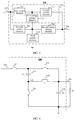
- FIG. 1 shows a typical buck circuit 100 that may be configured to perform buck conversion on an input voltage and then provide an input voltage obtained through buck conversion to a load R.
- the buck circuit 100 includes: an input terminal I, a power tube switch 110, a power tube switch 110, an inductor 130, a capacitor 120, and output terminals O1 and O2, where the inductor 130 and the capacitor 120 form a filter circuit.
- a control signal period T of the buck circuit 100 includes two time periods: tON and tOFF, where in the time period tON, the power tube switch 110 is in a closed state, and the power tube switch 110 is in an off state.
- the input voltage Vin is connected to the inductor 130 by using the endpoint LX, and the inductor 130 is in a charging and energy storage state.
- the power tube switch 110 is in an off state, the power tube switch 110 is in a closed state, the endpoint LX is grounded by using the power tube switch 110, and the inductor 130 is in a discharging state.
- Vout a voltage between the output terminals O1 and O2
- Vin is an input voltage, that is, a voltage of the input terminal I relative to ground
- D2 is a duty cycle that is equal to a ratio of tON to T
- IL is an inductance current
- lout is a load current
- key restraint factors of energy conversion efficiency of the buck circuit include: a loss of an inductive winding DCR that is equal to DCRxIL2, and a loss of a parasitic capacitor Cp at the endpoint LX that is equal to CpxViM2/2.
- An embodiment of the present invention provides a voltage converter, to reduce a circuit loss, and improve energy conversion efficiency.
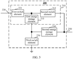
- FIG. 3 shows a voltage converter 200 according to an embodiment of this application.
- the voltage converter 200 may be configured to perform boost or buck conversion on an input voltage provided by a voltage source coupled to the voltage converter 200 and then provide an input voltage obtained through boost or buck conversion to a load coupled to the voltage converter 200.
- the load may be a terminal device, and this is not limited in this embodiment of this application.
- the voltage converter 200 may include an energy storage circuit 210, and the energy storage circuit 210 includes: a first switch element 211, a second switch element 212, and a first energy storage element 213.
- the voltage converter 200 further includes: a first external terminal 220, a third switch element 230, a second energy storage element 240, and a second external terminal 250.
- a first terminal of the first switch element 211 is coupled to the first external terminal 220, a second terminal of the first switch element 211 is coupled to a first terminal of the first energy storage element 213 and a first terminal of the second switch element 212, a second terminal of the second switch element 212 is coupled to the second external terminal 250, a second terminal of the first energy storage element 213 is coupled to a first terminal of the third switch element 230 and a first terminal of the second energy storage element 240, a second terminal of the second energy storage element 240 is coupled to the second external terminal 250, and a second terminal of the third switch element 230 is grounded.
- the first switch element 211 is in an on state
- the second switch element 212 and the third switch element 230 are in an off state
- a voltage source coupled to the voltage converter 200 charges the first energy storage element 213 and the second energy storage element 240.
- the first switch element 211 is in an off state
- the second switch element 212 and the third switch element 230 are in an on state
- the first energy storage element 213 and the second energy storage element 240 separately discharge to a load coupled to the voltage converter 200.
- the voltage converter 200 may include the first external terminal 220 and the second external terminal 250, where one of the first external terminal 220 and the second external terminal 250 may be configured to connect to the voltage source, and the other may be configured to connect to the load.
- the first external terminal 220 may be configured to connect to the load, and the second external terminal 250 may be configured to connect to the voltage source.
- the voltage converter 200 may be configured to perform boost conversion on an input voltage provided by the voltage source and then provide an input voltage obtained through boost conversion to the load, that is, the voltage converter 200 is a boost converter.
- the first external terminal 220 is configured to connect to the voltage source, and the second external terminal 250 is configured to connect to the load.
- the voltage converter 200 may be configured to perform buck conversion on an input voltage provided by the voltage source and then provide an input voltage obtained through buck conversion to the load, that is, the voltage converter 200 is a buck converter. This is not limited in this embodiment of this application.
- the first energy storage element 213 and the second energy storage element 240 may each be an element that can store energy and can release the stored energy, for example, a capacitor or an inductor.
- the first energy storage element 213 and the second energy storage element 240 may be of different device types.
- the first energy storage element 213 is a capacitor
- the second energy storage element 240 is an inductor, and this is not limited in this embodiment of this application.
- the voltage converter 200 may include one or more first energy storage elements 213, and the voltage converter 200 may include one or more second energy storage elements 240.
- FIG. 3 shows an example in which the voltage converter 200 includes one first energy storage element 213 and one second energy storage element 240. This embodiment of this application is not limited thereto.
- a conversion period (referred to as a first conversion period hereinafter) may include a first time period and a second time period, where the second time period may be after the first time period, and a length of the second time period may be equal to or not equal to a length of the first time period.
- the length of the first time period and the length of the second time period are not limited in this embodiment of this application.
- the voltage converter 200 may further include a capacitor CL, where one end of the capacitor may be connected to the second external terminal 250 of the voltage converter 200, and the other end of the capacitor may be grounded. If the second energy storage element is an inductor, the capacitor CL and the second energy storage element may form a filter circuit. This embodiment of this application is not limited thereto.
- the first switch element 211 may be in an on state, and both the second switch element 212 and the third switch element 230 may be in an off state, so that a first charging loop formed by sequentially connecting the voltage source, the first switch element 211, the first energy storage element 213, the second energy storage element 240, and the load in series is in an on state, and the first energy storage element 213 and the second energy storage element 240 are charged and store energy.
- the first switch element 211 may be in an off state, and the second switch element 212 and the third switch element 230 may be in an on state, so that the foregoing first charging loop is in an off state, a first discharging loop formed by sequentially connecting the first energy storage element 213, the second switch element 212, the load, and the third switch element 230 in series is in an on state, a second discharging loop formed by sequentially connecting the second energy storage element 240, the load, and the third switch element 230 in series is in an on state, and the first energy storage element 213 and the second energy storage element 240 discharge and release energy.
- This embodiment of this application is not limited thereto.
- the first energy storage element may release stored energy to the load by using the first discharging loop.
- an energy storage element in the first discharging loop may be the first energy storage element, that is, the first discharging loop may not include an energy storage element other than the first energy storage element.
- the second energy storage element may release stored energy to the load by using the second discharging loop.
- the first energy storage element and the second energy storage element may be connected in parallel in the second time period. This embodiment of this application is not limited thereto.
- the voltage converter 200 may include: a switch circuit, a first energy storage element, and a second energy storage element.
- the switch circuit may be configured to switch on the first charging loop in the first time period.
- the voltage source provides energy to the first energy storage element, the second energy storage element, and the load.
- both the first energy storage element and the second energy storage element may be in a charging and energy storage state.
- the voltage source may be connected to the first energy storage element, the second energy storage element, and the load in series. This embodiment of this application is not limited thereto.
- the switch circuit may be further configured to switch off the first charging loop in the second time period, and switch on the first discharging loop and the second discharging loop, where in the first discharging loop, the first energy storage element provides energy to the load, and in the second discharging loop, the second energy storage element provides energy to the load.
- both the first energy storage element and the second energy storage element may be in a discharging and energy release state.
- the switch circuit may include one or more switch elements.
- the switch circuit may include a first switch element, where the first switch element is connected in series in the first charging loop.
- the first switch element may be connected to the first energy storage element, the second energy storage element, and the load in series, and a connection order between the first switch element, the first energy storage element, the second energy storage element, and the load is not limited in this embodiment of this application.
- the first switch element may be configured to switch on or switch off the first charging loop.
- the first switch element may switch on the first charging loop in the first time period, and switch off the first charging loop in the second time period.
- the first switch element may be in an on state or in a closed state in the first time period, and be in an off state in the second time period. This embodiment of this application is not limited thereto.
- a first terminal of the first switch element may be connected to the first external terminal, and a second terminal of the first switch element may be connected to a first terminal of the first energy storage element.
- the second terminal of the first energy storage element may be connected to a first terminal of the second energy storage element, and a second terminal of the second energy storage element may be connected to the second external terminal.
- the switch circuit may include a second switch element, where the second switch element may be connected in series in the first discharging loop.
- the second switch element may be connected to the first energy storage element and the load in series, but a connection order between the second switch element, the first energy storage element, and the load is not limited in this embodiment of this application.
- the second switch element may be configured to switch on or switch off the first discharging loop.
- the second switch element may switch off the first discharging loop in the first time period, and switch on the first discharging loop in the second time period.
- the second switch element may be in an off state in the first time period, and be in an on state or in a closed state in the second time period. This embodiment of this application is not limited thereto.
- a first terminal of the second switch element may be connected to the first terminal of the first energy storage element, and a second terminal of the second switch element may be connected to the second external terminal of the voltage converter 200.
- the first terminal of the first energy storage element may be connected to the second terminal of the first switch element and the first terminal of the second switch element.
- the switch circuit may include a third switch element, where the third switch element may be connected in series in the second discharging loop.
- the third switch element may be connected to the second energy storage element and the load in series, but a connection order between the third switch element, the second energy storage element, and the load is not limited in this embodiment of this application.
- the third switch element may be configured to switch on or switch off the second discharging loop.
- the third switch element may switch off the second discharging loop in the first time period, and switch on the second discharging loop in the second time period.
- the third switch element may be in an off state in the first time period, and be in an on state or in a closed state in the second time period. This embodiment of this application is not limited thereto.
- the third switch element may be connected in series in both the first discharging loop and the second discharging loop.
- a first terminal of the third switch element may be connected to the second terminal of the first energy storage element, and a second terminal of the third switch element may be grounded.
- the second terminal of the first energy storage element may be separately connected to the first terminal of the second energy storage element and the first terminal of the third switch element.
- the energy storage circuit 210 may further include: M third energy storage elements 214 (a third energy storage element 1, ..., and a third energy storage element M), M fourth switch elements 215 (a fourth switch element 1, ..., and a fourth switch element M), M fifth switch elements 216 (a fifth switch element 1, ..., and a fifth switch element M), and M sixth switch elements 217 (a sixth switch element 1, ..., and a sixth switch element M), where M is an integer greater than or equal to 1.
- the third energy storage element 214 may be a device different from the first energy storage element 213 and the second energy storage element 240, or the third energy storage element 214 may be a device that is the same as the first energy storage element 213 or the second energy storage element 240. In an optional embodiment, the third energy storage element 214 may be a capacitor. This embodiment of this application is not limited thereto.
- a first terminal of the fourth switch element 1 may be coupled to a first terminal of the energy storage circuit 210, that is, the first terminal of the fourth switch element 1 may be coupled to the first external terminal, and a second terminal of the fourth switch element 1 may be connected to a first terminal of the third energy storage element 1 and a first terminal of the fifth switch element 1.
- a second terminal of the fifth switch element 1 may be connected to the second external terminal.
- a second terminal of the third energy storage element 1 may be connected to a first terminal of the fourth switch element 2 and a first terminal of the sixth switch element 1.
- a first terminal of the fourth switch element i may be connected to a second terminal of the third energy storage element i-1, and a second terminal of the fourth switch element i may be connected to a first terminal of the third energy storage element i and a first terminal of the fifth switch element i.
- a second terminal of the fifth switch element i may be connected to the second external terminal.
- a second terminal of the third energy storage element i may be connected to a first terminal of the sixth switch element i.
- some or all of the M third energy storage elements 214 may be in a charging and energy storage state in the first time period, and in a discharging and energy release state in the second time period. This embodiment of this application is not limited thereto.
- the M fourth switch elements may be connected in series in the first charging loop.
- the M fourth switch elements may be configured to switch on or switch off the first charging loop.
- all of the M fourth switch elements in the first time period, all of the M fourth switch elements may be in an on state, so that the first charging loop is in an on state.
- all of the M fourth switch elements in the second time period, all of the M fourth switch elements may be in an off state, so that the first charging loop is in an off state. This embodiment of this application is not limited thereto.
- the voltage source may be further configured to charge all of the M third energy storage elements.
- the M third energy storage elements 214 may be connected in series.
- the M third energy storage elements 214 may be further connected to the first external terminal of the voltage converter, the M fourth switch elements, the first switch element 211, the first energy storage element 213, the second energy storage element 240, and the load in series.
- each third energy storage element 214 in a discharging state may correspond to a discharging loop that is referred to as a third discharging loop below.
- the M third discharging loops may be in a one-to-one correspondence with the M third energy storage elements, and in each third discharging loop, a corresponding third energy storage element may release stored energy to the load. This embodiment of this application is not limited thereto.
- the M fifth switch elements 214 may be in a one-to-one correspondence with the M third energy storage elements 214, where each fifth switch element 214 may be configured to switch on or switch off a third discharging loop including a corresponding third energy storage element 214. In the third discharging loop, the fifth switch element 214 may be connected in series to the corresponding third energy storage element 214. In an optional embodiment, each fifth switch element 214 may be configured to switch off, in the first time period, the third discharging loop including the corresponding third energy storage element 214, and switch on, in the second time period, the third discharging loop including the corresponding third energy storage element 214. For example, each fifth switch element may be in an off state in the first time period, and be in an on state in the second time period. This embodiment of this application is not limited thereto.
- the M sixth switch elements may be in a one-to-one correspondence with the M third energy storage elements 214, and each sixth switch element may be configured to switch on or switch off a third discharging loop including a corresponding third energy storage element 214.
- the sixth switch element may be connected in series to the corresponding third energy storage element 214.
- the sixth switch element may be configured to switch off, in the first time period, the third discharging loop including the corresponding third energy storage element 214, and switch on, in the second time period, the third discharging loop including the corresponding third energy storage element 214.
- each sixth switch element may be in an off state in the first time period, and be in an on state in the second time period. This embodiment of this application is not limited thereto.
- the third discharging loop formed by connecting the third energy storage element i, the fifth switch element i, the sixth switch element i, and the load in series is switched on, and the third energy storage element i provides energy to the load.
- This embodiment of this application is not limited thereto.
- the energy storage circuit 210 includes the M fourth switch elements, the M fifth switch elements, and the M sixth switch elements.
- quantities of fourth switch elements, fifth switch elements, and sixth switch elements included in the energy storage circuit 210 are not limited in this embodiment of this application.
- the voltage converter 200 may further include a seventh switch element 260, and the seventh switch element 260 may be configured to enable an energy storage element (for example, the first energy storage element 213, or the first energy storage element 213 and M third energy storage elements 214) in the energy storage circuit 210 to be in an operating state or a bypass state.
- the voltage converter 200 may operate in a first operating mode.
- the voltage converter 200 may operate in a second operating mode.
- a second charging loop may be in an on state in a third time period, where in the second charging loop, the voltage source provides energy to the second energy storage element 240 and the load, and the second energy storage element is charged and stores energy.
- the second charging loop may not include the energy storage element in the energy storage circuit 210.
- the second charging loop in a fourth time period following the third time period, the second charging loop may be in an off state, the second discharging loop may be in an on state, and the second energy storage element 240 provides energy to the load.
- This embodiment of this application is not limited thereto.
- the voltage converter 200 may have a second conversion period, and the second conversion period may include the third time period and the fourth time period following the third time period.
- the second conversion period may be the same as or different from the first conversion period
- a length of the first time period may be the same as or different from that of the third time period
- a length of the second time period may be the same as or different from that of the fourth time period. This is not limited in this embodiment of this application.
- a first terminal of the seventh switch element 260 may be connected to the first external terminal, and a second terminal of the seventh switch element 260 may be connected to the second terminal of the first energy storage element 213, the first terminal of the second energy storage element 240, and the first terminal of the third switch element 230.
- This embodiment of this application is not limited thereto.
- the first switch element 211 and the second switch element 212 may always keep an off state.
- the seventh switch element 260 may be in an on state, and the third switch element 230 may be in an off state, so that the second charging loop formed by sequentially connecting the voltage source, the seventh switch element 260, the second energy storage element 240, and the load in series is in an on state, and the second energy storage element 240 is charged and stores energy.
- the seventh switch element 260 may be in an off state, and the third switch element 230 may be in an on state, so that the second charging loop is in an off state, the second discharging loop formed by the second energy storage element 240, the load, and the third switch element 230 is in an on state, and the second energy storage element 240 discharges and releases energy.
- This embodiment of this application is not limited thereto.
- a switch element in this embodiment of this application may be a device such as a semiconductor MOSFET transistor, a semiconductor rectifier, or a semiconductor diode. This is not limited in this embodiment of this application.
- the voltage converter 200 may further include a controller, configured to send a driving signal to each switch element in the voltage converter 200, so as to control a status of the switch element.
- the controller may be specifically a control circuit or a control chip. This is not limited in this embodiment of this application.
- FIG. 6 shows an example of a voltage converter 300 according to an embodiment of this application. It is assumed herein that the voltage converter 300 is a buck converter. As shown in FIG. 6 , the voltage converter 300 includes: a first external terminal 320 configured to connect to a voltage source, a power tube switch 311, a power tube switch 312, a capacitor 313, a power tube switch 330, an inductor 340, a capacitor 370, and a second external terminal 350 configured to connect to a load, where the inductor 340 and the capacitor 370 form a filter circuit.
- the first energy storage element is a capacitor CF
- the second energy storage element is an inductor L
- each switch element is a power tube switch.
- the power tube switch 311 may be in an on state, and the power tube switch 312 and the power tube switch 330 may be in an off state, so that a first charging loop formed by connecting the voltage source coupled to the first external terminal, the power tube switch 311, the capacitor 313, the inductor 340, and the load R coupled to the second external terminal in series is in an on state, and both the capacitor 313 and the inductor 340 are in a charging and energy storage state.
- the power tube switch 311 may be in an off state, and the power tube switch 312 and the power tube switch 330 are in an on state, so that the first charging loop is in an off state, a first discharging loop formed by connecting the capacitor 313, the power tube switch 312, the load R, and the power tube switch 330 in series is in an on state, the capacitor 313 releases stored energy by using the first discharging loop, a second discharging loop formed by connecting the inductor 340, the load R, and the power tube switch 330 in series is in an on state, and the inductor 340 releases stored energy by using the second discharging loop.
- FIG. 6 shows an example in which the voltage converter 300 includes a capacitor CF.
- the voltage converter 300 may include N capacitors CF, each of the N capacitors C may be in a charging state in the first time period, corresponds to a discharging loop in the second time period, and releases stored energy to the load by using the corresponding discharging loop.
- N may be equal to M+1, that is, each of the foregoing M third energy storage elements may be a capacitor CF.
- Vout a voltage of the output load, that is, an output voltage of the voltage converter
- Vin is the voltage source, that is, an input voltage provided by the voltage source to the voltage converter
- D1 is a duty cycle that is equal to a ratio of the first time period to a first conversion period
- IL is an inductance current
- lout is an output current.
- An embodiment of this application further provides a voltage conversion system.
- the voltage conversion system may include any voltage converter described above, and a voltage source and a load that are coupled to the voltage converter.
- the voltage conversion system may include any voltage converter described above, and a voltage source and a load that are coupled to the voltage converter.
- the voltage converters provided in the embodiments of this application are described in detail above with reference to FIG. 2 to FIG. 6 , and a method for controlling a voltage converter provided in an embodiment of this application is described in detail below with reference to FIG. 7 .
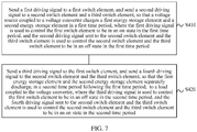
- FIG. 7 shows a method 400 for controlling a voltage converter according to an embodiment of this application.
- the voltage converter may be specifically any voltage converter 200 described above, and this is not limited in this embodiment of this application.
- the method 400 includes the following steps.
- S410 Send a first driving signal to a first switch element, and send a second driving signal to a second switch element and a third switch element, so that a voltage source coupled to a voltage converter charges a first energy storage element and a second energy storage element in a first time period, where the first driving signal is used to control the first switch element to be in an on state in the first time period, and the second driving signal sent to the second switch element and the third switch element is used to control the second switch element and the third switch element to be in an off state in the first time period.
- S420 Send a third driving signal to the first switch element, and send a fourth driving signal to the second switch element and the third switch element, so that the first energy storage element and the second energy storage element separately discharge, in a second time period following the first time period, to a load coupled to the voltage converter, where the third driving signal is used to control the first switch element to be in an off state in the second time period, and the fourth driving signal sent to the second switch element and the third switch element is used to control the second switch element and the third switch element to be in an on state in the second time period.
- a controller may send driving signals to switch elements simultaneously or in any order.
- S410 and S420 may be performed simultaneously or S410 may be performed before S420. This is not limited in this embodiment of this application.
- the first driving signal and the second driving signal may be a same signal or different signals
- the third driving signal and the fourth driving signal may be a same signal or different signals. This is not limited in this embodiment of this application.
- the method 400 further includes: sending, by the controller, a fifth control signal to the seventh switch element, where the fifth control signal is used to control the seventh switch element to be in an off state in both the first time period and the second time period.
- the method 400 further includes:
- control method 400 includes: sending a first driving signal to a switch circuit in the voltage converter, to enable the switch circuit to switch on a first charging loop in the first time period, where in the first charging loop, the voltage source coupled to the voltage converter provides energy to the first energy storage element, the second energy storage element, and the load; and sending a second driving signal to the switch circuit, to enable the switch circuit to switch off the first charging loop and switch on a first discharging loop and a second discharging loop in the second time period following the first time period, where in the first discharging loop, the first energy storage element provides energy to the load, and in the second discharging loop, the second energy storage element provides energy to the load.
- the first driving signal and the second driving signal may be respectively sent in the first time period and the second time period, or may be sent simultaneously or sent in any order. This is not limited in this embodiment of this application.
- the first driving signal may be used to control the first switch element to be in an on state in the first time period
- the second driving signal may be used to control the first switch element to be in an off state in the second time period.
- the first driving signal may be used to control the second switch element to be in an off state in the first time period
- the second driving signal may be used to control the second switch element to be in an on state in the second time period.
- the first driving signal may be used to control the third switch element to be in an off state in the first time period
- the second driving signal may be used to control the third switch element to be in an on state in the second time period.
- the method 400 may further include: sending the third driving signal to the seventh switch element, to enable the seventh switch element to be in an off state.
- the method 400 may further include: sending the fourth driving signal to the seventh switch element, to enable the seventh switch element to bypass the first energy storage element.
- the method may further include: sending a fifth driving signal to the switch circuit, to enable the switch circuit to switch on a second charging loop in a third time period; and sending a sixth driving signal to the switch circuit, to enable the switch circuit to switch off the second charging loop and switch on the second discharging loop in a fourth time period following the third time period, where in the second charging loop, the voltage source provides energy to the second energy storage element and the load.
- the method 400 may be performed by the controller in the foregoing embodiment. To avoid repetition, details are not described herein again.
- sequence numbers of the foregoing processes do not indicate an execution sequence, and an execution sequence of processes shall be determined based on functions and internal logic of the processes, and shall constitute no limitation on an implementation process of the embodiments of this application.
- a is connected to B may indicate that A is directly connected to B or that A is indirectly connected to B.
- system and “network” in this specification are usually interchangeably used in this specification.
- the term “and/or” in this specification describes only an association relationship for describing associated objects and represents that three relationships may exist. For example, A and/or B may represent the following three cases: Only A exists, both A and B exist, and only B exists.
- the character “/” in this specification generally indicates an “or” relationship between the associated objects.
- the disclosed system, apparatus, and method may be implemented in other manners.
- the described apparatus embodiment is merely an example.
- the unit division is merely logical function division and may be other division in actual implementation.
- a plurality of units or components may be combined or integrated into another system, or some features may be ignored or not performed.
- the displayed or discussed mutual couplings or direct couplings or communication connections may be implemented by using some interfaces.
- the indirect couplings or communication connections between the apparatuses or units may be implemented in electrical, mechanical, or other forms.
- the units described as separate parts may or may not be physically separate, and parts displayed as units may or may not be physical units, may be located in one position, or may be distributed on a plurality of network units. Some or all of the units may be selected based on actual requirements to achieve the objectives of the solutions of the embodiments.
- the functions When the functions are implemented in the form of a software functional unit and sold or used as an independent product, the functions may be stored in a computer-readable storage medium. Based on such an understanding, the technical solutions of this application essentially, or the part contributing to the prior art, or some of the technical solutions may be implemented in a form of a software product.
- the software product is stored in a storage medium, and includes several instructions for instructing a computer device (which may be a personal computer, a server, or a network device) to perform all or some of the steps of the methods described in the embodiments of this application.
- the foregoing storage medium includes: any medium that can store program code, such as a USB flash drive, a removable hard disk, a read-only memory (Read-Only Memory, ROM), a random access memory (Random Access Memory, RAM), a magnetic disk, or an optical disc.
- program code such as a USB flash drive, a removable hard disk, a read-only memory (Read-Only Memory, ROM), a random access memory (Random Access Memory, RAM), a magnetic disk, or an optical disc.
Landscapes
- Engineering & Computer Science (AREA)
- Power Engineering (AREA)
- Dc-Dc Converters (AREA)
- External Artificial Organs (AREA)
Applications Claiming Priority (2)
| Application Number | Priority Date | Filing Date | Title |
|---|---|---|---|
| CN201710113455.8A CN106685219B (zh) | 2017-02-28 | 2017-02-28 | 电压转换器及其控制方法和电压转换系统 |
| PCT/CN2018/077093 WO2018157761A1 (fr) | 2017-02-28 | 2018-02-24 | Convertisseur de tension et son procédé de commande et son système de conversion de tension |
Publications (3)
| Publication Number | Publication Date |
|---|---|
| EP3565097A4 EP3565097A4 (fr) | 2019-11-06 |
| EP3565097A1 true EP3565097A1 (fr) | 2019-11-06 |
| EP3565097B1 EP3565097B1 (fr) | 2025-10-01 |
Family
ID=58862759
Family Applications (1)
| Application Number | Title | Priority Date | Filing Date |
|---|---|---|---|
| EP18760773.4A Active EP3565097B1 (fr) | 2017-02-28 | 2018-02-24 | Convertisseur de tension et son procédé de commande et son système de conversion de tension |
Country Status (4)
| Country | Link |
|---|---|
| US (1) | US10826395B2 (fr) |
| EP (1) | EP3565097B1 (fr) |
| CN (2) | CN110611424B (fr) |
| WO (1) | WO2018157761A1 (fr) |
Cited By (2)
| Publication number | Priority date | Publication date | Assignee | Title |
|---|---|---|---|---|
| EP3627650A4 (fr) * | 2017-06-08 | 2020-05-13 | Huawei Technologies Co., Ltd. | Circuit de conversion d'alimentation électrique, dispositif de charge et système |
| EP3627676A4 (fr) * | 2017-06-19 | 2020-06-24 | Huawei Technologies Co., Ltd. | Circuit de conversion de puissance, et appareil et système de charge |
Families Citing this family (12)
| Publication number | Priority date | Publication date | Assignee | Title |
|---|---|---|---|---|
| CN110611424B (zh) | 2017-02-28 | 2021-10-26 | 华为技术有限公司 | 电压转换器及其控制方法和电压转换系统 |
| CN108988630B (zh) * | 2017-06-01 | 2021-03-30 | 华为技术有限公司 | 一种电源转换电路及相关装置和终端设备 |
| TWI649939B (zh) * | 2017-07-07 | 2019-02-01 | 財團法人工業技術研究院 | 電源裝置運作方法、電源裝置及電源裝置管理系統 |
| CN107834844B (zh) | 2017-10-19 | 2020-04-03 | 华为技术有限公司 | 一种开关电容变换电路、充电控制系统及控制方法 |
| CN111869072B (zh) * | 2018-08-01 | 2021-10-01 | 华为技术有限公司 | 一种电压转换电路的控制电路 |
| DE102020200927A1 (de) | 2020-01-27 | 2021-07-29 | Dialog Semiconductor (Uk) Limited | Hybrid-Mehrpegel-Leistungsumsetzer mit lnduktor zwischen Stufen |
| US11456663B2 (en) * | 2020-06-12 | 2022-09-27 | Dialog Semiconductor (Uk) Limited | Power converter with reduced root mean square input current |
| US11637491B2 (en) | 2020-12-03 | 2023-04-25 | Dialog Semiconductor (Uk) Limited | Multi-stage power converter |
| US11496051B2 (en) | 2020-12-16 | 2022-11-08 | Dialog Semiconductor (Uk) Limited | Power converter |
| US11967901B2 (en) | 2021-12-09 | 2024-04-23 | Renesas Design (UK) Limited | Hybrid multi-phase power converter with phase shedding |
| CN115037011A (zh) * | 2022-04-19 | 2022-09-09 | 伏达半导体(合肥)有限公司 | 双电池充电装置、方法及其控制器 |
| TWI846555B (zh) * | 2023-08-01 | 2024-06-21 | 台達電子工業股份有限公司 | 可平衡能量與混合供電的電源轉換器與電源轉換方法 |
Family Cites Families (35)
| Publication number | Priority date | Publication date | Assignee | Title |
|---|---|---|---|---|
| US5680300A (en) * | 1995-12-22 | 1997-10-21 | Analog Devices, Inc. | Regulated charge pump DC/DC converter |
| US6304068B1 (en) * | 2000-04-20 | 2001-10-16 | City University Of Hong Kong | Bi-directional switched-capacitor based voltage converter |
| US7239194B2 (en) * | 2004-03-25 | 2007-07-03 | Integral Wave Technologies, Inc. | Trench capacitor power supply system and method |
| US7230405B2 (en) * | 2004-10-26 | 2007-06-12 | Delta Electronics, Inc. | Non-isolated power conversion system having multiple switching power converters |
| US7408328B2 (en) * | 2005-08-02 | 2008-08-05 | Dell Products L.P. | Information handling system including a power supply unit with a switching regulator that reduces transient load release |
| EP2043243A1 (fr) * | 2007-09-27 | 2009-04-01 | ABB Schweiz AG | Circuit convertisseur ainsi que procédé de fonctionnement d'un tel circuit convertisseur |
| GB2455524B (en) * | 2007-12-11 | 2010-04-07 | Wolfson Microelectronics Plc | Charge pump circuit and methods of operation thereof and portable audio apparatus including charge pump circuits |
| TWI358884B (en) * | 2008-06-13 | 2012-02-21 | Green Solution Tech Co Ltd | Dc/dc converter circuit and charge pump controller |
| CN101355302B (zh) * | 2008-09-16 | 2011-12-14 | 北京交通大学 | L型降压变换器的拓扑结构 |
| CN101355303B (zh) * | 2008-09-16 | 2011-12-14 | 北京交通大学 | T型降压变换器的拓扑结构 |
| WO2010151884A2 (fr) * | 2009-06-27 | 2010-12-29 | Asic Advantage, Inc. | Convertisseur de suralimentation d'inducteur couplé en mode limite |
| US9467053B2 (en) * | 2009-07-09 | 2016-10-11 | Infineon Technologies Ag | Controlling a multi-mode switching converter |
| US20110018619A1 (en) * | 2009-07-22 | 2011-01-27 | Qualcomm Incorporated | Integrated negative voltage generator |
| FR2959624A1 (fr) * | 2010-04-28 | 2011-11-04 | St Ericsson Sa | Circuit de conversion de tension continue |
| US20110285369A1 (en) | 2010-05-20 | 2011-11-24 | Cuks, Llc | Three-switch step-down converter |
| EP2466738B1 (fr) * | 2010-12-20 | 2018-04-04 | ams AG | Convertisseur de tension et procédé de conversion de tension |
| US8680795B2 (en) * | 2011-06-03 | 2014-03-25 | Ford Global Technologies, Llc | Vehicle electric drive and power systems |
| CN102377324B (zh) * | 2011-10-18 | 2013-09-04 | 吕遥 | 适合于高压应用的变流桥臂及其应用系统 |
| US9111601B2 (en) * | 2012-06-08 | 2015-08-18 | Qualcomm Incorporated | Negative voltage generators |
| TWI497254B (zh) * | 2012-07-19 | 2015-08-21 | Alpha Imaging Technology Corp | 開關電路及應用其之充電幫浦 |
| US9160166B2 (en) * | 2012-12-19 | 2015-10-13 | Silicon Laboratories Inc. | Charge pump for low power consumption apparatus and associated methods |
| CN104283417B (zh) * | 2013-07-12 | 2017-06-27 | 华硕电脑股份有限公司 | 多相降压直流转换器 |
| US8981838B1 (en) * | 2013-09-13 | 2015-03-17 | Himax Technologies Limited | Half-ratio charge pump circuit |
| TWI495242B (zh) * | 2013-10-09 | 2015-08-01 | Nat Univ Tsing Hua | 雙向直流轉換器 |
| US9385600B2 (en) * | 2013-11-22 | 2016-07-05 | Texas Instruments Incorporated | Low-loss step-up and step-down voltage converter |
| US9912297B2 (en) * | 2015-07-01 | 2018-03-06 | Qorvo Us, Inc. | Envelope tracking power converter circuitry |
| CN105141131A (zh) * | 2015-08-12 | 2015-12-09 | 周耀瑜 | 电感电容串联扩流的开关电源 |
| TWI551019B (zh) * | 2015-10-15 | 2016-09-21 | 瑞昱半導體股份有限公司 | 電荷幫浦及包含其之動態電荷幫浦裝置 |
| JP2017118607A (ja) * | 2015-12-21 | 2017-06-29 | 株式会社東芝 | チャージポンプ回路および降圧型レギュレータ回路 |
| US9973147B2 (en) * | 2016-05-10 | 2018-05-15 | Qorvo Us, Inc. | Envelope tracking power management circuit |
| CN106208698B (zh) * | 2016-08-09 | 2018-11-09 | 中南大学 | 设有软开关的四开关Buck-Boost变换器电路及其控制方法 |
| CN110611424B (zh) * | 2017-02-28 | 2021-10-26 | 华为技术有限公司 | 电压转换器及其控制方法和电压转换系统 |
| CN109038694B (zh) * | 2017-06-08 | 2020-02-21 | 华为技术有限公司 | 电源转换电路、充电装置及系统 |
| CN111371290B (zh) * | 2017-06-19 | 2025-01-14 | 华为技术有限公司 | 电源转换电路、充电装置及系统 |
| US10505444B1 (en) * | 2018-10-04 | 2019-12-10 | Xilinx, Inc. | Voltage divider and method of implementing a voltage divider |
-
2017
- 2017-02-28 CN CN201910877600.9A patent/CN110611424B/zh active Active
- 2017-02-28 CN CN201710113455.8A patent/CN106685219B/zh not_active Expired - Fee Related
-
2018
- 2018-02-24 WO PCT/CN2018/077093 patent/WO2018157761A1/fr not_active Ceased
- 2018-02-24 EP EP18760773.4A patent/EP3565097B1/fr active Active
-
2019
- 2019-08-13 US US16/539,573 patent/US10826395B2/en active Active
Cited By (3)
| Publication number | Priority date | Publication date | Assignee | Title |
|---|---|---|---|---|
| EP3627650A4 (fr) * | 2017-06-08 | 2020-05-13 | Huawei Technologies Co., Ltd. | Circuit de conversion d'alimentation électrique, dispositif de charge et système |
| EP4131714A3 (fr) * | 2017-06-08 | 2023-04-26 | Huawei Technologies Co., Ltd. | Circuit de conversion de puissance et appareil de chargement et système |
| EP3627676A4 (fr) * | 2017-06-19 | 2020-06-24 | Huawei Technologies Co., Ltd. | Circuit de conversion de puissance, et appareil et système de charge |
Also Published As
| Publication number | Publication date |
|---|---|
| EP3565097A4 (fr) | 2019-11-06 |
| WO2018157761A1 (fr) | 2018-09-07 |
| CN110611424B (zh) | 2021-10-26 |
| US10826395B2 (en) | 2020-11-03 |
| CN110611424A (zh) | 2019-12-24 |
| CN106685219A (zh) | 2017-05-17 |
| US20190372462A1 (en) | 2019-12-05 |
| CN106685219B (zh) | 2019-10-01 |
| EP3565097B1 (fr) | 2025-10-01 |
Similar Documents
| Publication | Publication Date | Title |
|---|---|---|
| US10826395B2 (en) | Voltage converter, method for controlling voltage converter, and voltage conversion system | |
| US10790742B1 (en) | Multi-level power converter with improved transient load response | |
| EP3499679A1 (fr) | Système, procédé et circuit de charge, et dispositif électronique | |
| CN104052278B (zh) | 多电平增压变换器拓扑、控制和软启动系统及方法 | |
| CN107959421B (zh) | Buck-boost型直流转换器及其控制方法 | |
| US8581561B2 (en) | DC-DC boost converter circuit with an output stabilization circuit and method for driving the same | |
| US20090085548A1 (en) | Converter circuit and method for operating such a converter circuit | |
| CN104184200A (zh) | 电源适配器、电源适配器的控制方法及笔记本 | |
| EP4604377A1 (fr) | Convertisseur abaisseur-élévateur et système d'alimentation électrique | |
| US12301108B2 (en) | Cascade switched capacitor converter to reduce switching loss | |
| CN111697647A (zh) | 一种充电电路及终端、充电电路的控制方法及装置 | |
| CN115912533A (zh) | 包括自举电容器的降压转换器及其操作方法 | |
| EP3627650B1 (fr) | Circuit de conversion d'alimentation électrique, dispositif de charge et système | |
| CN216900809U (zh) | 一种芯片的测试电路及测试系统 | |
| CN204376508U (zh) | 一种快速充电电路 | |
| CN215912033U (zh) | 电压变换电路和电子设备 | |
| US20220124888A1 (en) | Buck topological circuit for power supply | |
| US20250070661A1 (en) | Direct current-direct current converter and electronic device | |
| CN111697646A (zh) | 切换式充电电路及终端、切换式充电电路的控制方法 | |
| KR20110088057A (ko) | 스위칭 배열과 충방전을 이용한 고효율 충전장치 | |
| CN117578882A (zh) | 单模式双电流通路的降压-升压转换器的控制电路及方法 | |
| CN215120579U (zh) | 开关电源电路、驱动装置和电力电子功率开关 | |
| CN120749968B (zh) | 储能系统中电池的充电方法、装置及存储介质 | |
| EP4047799B1 (fr) | Procédé de commande et organe de commande pour convertisseurs de commutation simo | |
| EP4580017A1 (fr) | Convertisseur de puissance et procédé de commande |
Legal Events
| Date | Code | Title | Description |
|---|---|---|---|
| STAA | Information on the status of an ep patent application or granted ep patent |
Free format text: STATUS: THE INTERNATIONAL PUBLICATION HAS BEEN MADE |
|
| PUAI | Public reference made under article 153(3) epc to a published international application that has entered the european phase |
Free format text: ORIGINAL CODE: 0009012 |
|
| STAA | Information on the status of an ep patent application or granted ep patent |
Free format text: STATUS: REQUEST FOR EXAMINATION WAS MADE |
|
| 17P | Request for examination filed |
Effective date: 20190801 |
|
| A4 | Supplementary search report drawn up and despatched |
Effective date: 20190927 |
|
| AK | Designated contracting states |
Kind code of ref document: A1 Designated state(s): AL AT BE BG CH CY CZ DE DK EE ES FI FR GB GR HR HU IE IS IT LI LT LU LV MC MK MT NL NO PL PT RO RS SE SI SK SM TR |
|
| AX | Request for extension of the european patent |
Extension state: BA ME |
|
| DAV | Request for validation of the european patent (deleted) | ||
| DAX | Request for extension of the european patent (deleted) | ||
| STAA | Information on the status of an ep patent application or granted ep patent |
Free format text: STATUS: EXAMINATION IS IN PROGRESS |
|
| 17Q | First examination report despatched |
Effective date: 20211019 |
|
| GRAP | Despatch of communication of intention to grant a patent |
Free format text: ORIGINAL CODE: EPIDOSNIGR1 |
|
| STAA | Information on the status of an ep patent application or granted ep patent |
Free format text: STATUS: GRANT OF PATENT IS INTENDED |
|
| RIC1 | Information provided on ipc code assigned before grant |
Ipc: H02M 1/00 20060101ALI20231003BHEP Ipc: H02M 3/158 20060101ALI20231003BHEP Ipc: H02M 3/07 20060101AFI20231003BHEP |
|
| INTG | Intention to grant announced |
Effective date: 20231108 |
|
| GRAJ | Information related to disapproval of communication of intention to grant by the applicant or resumption of examination proceedings by the epo deleted |
Free format text: ORIGINAL CODE: EPIDOSDIGR1 |
|
| STAA | Information on the status of an ep patent application or granted ep patent |
Free format text: STATUS: EXAMINATION IS IN PROGRESS |
|
| INTC | Intention to grant announced (deleted) | ||
| GRAP | Despatch of communication of intention to grant a patent |
Free format text: ORIGINAL CODE: EPIDOSNIGR1 |
|
| STAA | Information on the status of an ep patent application or granted ep patent |
Free format text: STATUS: GRANT OF PATENT IS INTENDED |
|
| INTG | Intention to grant announced |
Effective date: 20250521 |
|
| P01 | Opt-out of the competence of the unified patent court (upc) registered |
Free format text: CASE NUMBER: APP_25663/2025 Effective date: 20250528 |
|
| GRAS | Grant fee paid |
Free format text: ORIGINAL CODE: EPIDOSNIGR3 |
|
| GRAA | (expected) grant |
Free format text: ORIGINAL CODE: 0009210 |
|
| STAA | Information on the status of an ep patent application or granted ep patent |
Free format text: STATUS: THE PATENT HAS BEEN GRANTED |
|
| AK | Designated contracting states |
Kind code of ref document: B1 Designated state(s): AL AT BE BG CH CY CZ DE DK EE ES FI FR GB GR HR HU IE IS IT LI LT LU LV MC MK MT NL NO PL PT RO RS SE SI SK SM TR |
|
| REG | Reference to a national code |
Ref country code: GB Ref legal event code: FG4D Ref country code: CH Ref legal event code: F10 Free format text: ST27 STATUS EVENT CODE: U-0-0-F10-F00 (AS PROVIDED BY THE NATIONAL OFFICE) Effective date: 20251001 |
|
| REG | Reference to a national code |
Ref country code: IE Ref legal event code: FG4D |
|
| REG | Reference to a national code |
Ref country code: DE Ref legal event code: R096 Ref document number: 602018086025 Country of ref document: DE |
|
| REG | Reference to a national code |
Ref country code: NL Ref legal event code: MP Effective date: 20251001 |
|
| REG | Reference to a national code |
Ref country code: AT Ref legal event code: MK05 Ref document number: 1843593 Country of ref document: AT Kind code of ref document: T Effective date: 20251001 |
|
| PG25 | Lapsed in a contracting state [announced via postgrant information from national office to epo] |
Ref country code: NL Free format text: LAPSE BECAUSE OF FAILURE TO SUBMIT A TRANSLATION OF THE DESCRIPTION OR TO PAY THE FEE WITHIN THE PRESCRIBED TIME-LIMIT Effective date: 20251001 |
|
| PGFP | Annual fee paid to national office [announced via postgrant information from national office to epo] |
Ref country code: GB Payment date: 20260106 Year of fee payment: 9 |
|
| PG25 | Lapsed in a contracting state [announced via postgrant information from national office to epo] |
Ref country code: ES Free format text: LAPSE BECAUSE OF FAILURE TO SUBMIT A TRANSLATION OF THE DESCRIPTION OR TO PAY THE FEE WITHIN THE PRESCRIBED TIME-LIMIT Effective date: 20251001 |
|
| REG | Reference to a national code |
Ref country code: LT Ref legal event code: MG9D |
|
| PG25 | Lapsed in a contracting state [announced via postgrant information from national office to epo] |
Ref country code: NO Free format text: LAPSE BECAUSE OF FAILURE TO SUBMIT A TRANSLATION OF THE DESCRIPTION OR TO PAY THE FEE WITHIN THE PRESCRIBED TIME-LIMIT Effective date: 20260101 |
|
| PGFP | Annual fee paid to national office [announced via postgrant information from national office to epo] |
Ref country code: DE Payment date: 20260102 Year of fee payment: 9 |
|
| PG25 | Lapsed in a contracting state [announced via postgrant information from national office to epo] |
Ref country code: AT Free format text: LAPSE BECAUSE OF FAILURE TO SUBMIT A TRANSLATION OF THE DESCRIPTION OR TO PAY THE FEE WITHIN THE PRESCRIBED TIME-LIMIT Effective date: 20251001 Ref country code: FI Free format text: LAPSE BECAUSE OF FAILURE TO SUBMIT A TRANSLATION OF THE DESCRIPTION OR TO PAY THE FEE WITHIN THE PRESCRIBED TIME-LIMIT Effective date: 20251001 Ref country code: HR Free format text: LAPSE BECAUSE OF FAILURE TO SUBMIT A TRANSLATION OF THE DESCRIPTION OR TO PAY THE FEE WITHIN THE PRESCRIBED TIME-LIMIT Effective date: 20251001 |
|
| PG25 | Lapsed in a contracting state [announced via postgrant information from national office to epo] |
Ref country code: RS Free format text: LAPSE BECAUSE OF FAILURE TO SUBMIT A TRANSLATION OF THE DESCRIPTION OR TO PAY THE FEE WITHIN THE PRESCRIBED TIME-LIMIT Effective date: 20260101 |
|
| PG25 | Lapsed in a contracting state [announced via postgrant information from national office to epo] |
Ref country code: IS Free format text: LAPSE BECAUSE OF FAILURE TO SUBMIT A TRANSLATION OF THE DESCRIPTION OR TO PAY THE FEE WITHIN THE PRESCRIBED TIME-LIMIT Effective date: 20260201 |
|
| PG25 | Lapsed in a contracting state [announced via postgrant information from national office to epo] |
Ref country code: PT Free format text: LAPSE BECAUSE OF FAILURE TO SUBMIT A TRANSLATION OF THE DESCRIPTION OR TO PAY THE FEE WITHIN THE PRESCRIBED TIME-LIMIT Effective date: 20260202 Ref country code: CZ Free format text: LAPSE BECAUSE OF FAILURE TO SUBMIT A TRANSLATION OF THE DESCRIPTION OR TO PAY THE FEE WITHIN THE PRESCRIBED TIME-LIMIT Effective date: 20251001 |
|
| PG25 | Lapsed in a contracting state [announced via postgrant information from national office to epo] |
Ref country code: PL Free format text: LAPSE BECAUSE OF FAILURE TO SUBMIT A TRANSLATION OF THE DESCRIPTION OR TO PAY THE FEE WITHIN THE PRESCRIBED TIME-LIMIT Effective date: 20251001 |
|
| PG25 | Lapsed in a contracting state [announced via postgrant information from national office to epo] |
Ref country code: LV Free format text: LAPSE BECAUSE OF FAILURE TO SUBMIT A TRANSLATION OF THE DESCRIPTION OR TO PAY THE FEE WITHIN THE PRESCRIBED TIME-LIMIT Effective date: 20251001 |
|
| PG25 | Lapsed in a contracting state [announced via postgrant information from national office to epo] |
Ref country code: BG Free format text: LAPSE BECAUSE OF FAILURE TO SUBMIT A TRANSLATION OF THE DESCRIPTION OR TO PAY THE FEE WITHIN THE PRESCRIBED TIME-LIMIT Effective date: 20251001 |