EP3567005A1 - Hexagonale bornitrid-dünnschicht und verfahren zur herstellung davon - Google Patents
Hexagonale bornitrid-dünnschicht und verfahren zur herstellung davon Download PDFInfo
- Publication number
- EP3567005A1 EP3567005A1 EP18735883.3A EP18735883A EP3567005A1 EP 3567005 A1 EP3567005 A1 EP 3567005A1 EP 18735883 A EP18735883 A EP 18735883A EP 3567005 A1 EP3567005 A1 EP 3567005A1
- Authority
- EP
- European Patent Office
- Prior art keywords
- thin film
- boron nitride
- hexagonal boron
- nitride thin
- metal
- Prior art date
- Legal status (The legal status is an assumption and is not a legal conclusion. Google has not performed a legal analysis and makes no representation as to the accuracy of the status listed.)
- Pending
Links
Images


Classifications
-
- C—CHEMISTRY; METALLURGY
- C23—COATING METALLIC MATERIAL; COATING MATERIAL WITH METALLIC MATERIAL; CHEMICAL SURFACE TREATMENT; DIFFUSION TREATMENT OF METALLIC MATERIAL; COATING BY VACUUM EVAPORATION, BY SPUTTERING, BY ION IMPLANTATION OR BY CHEMICAL VAPOUR DEPOSITION, IN GENERAL; INHIBITING CORROSION OF METALLIC MATERIAL OR INCRUSTATION IN GENERAL
- C23C—COATING METALLIC MATERIAL; COATING MATERIAL WITH METALLIC MATERIAL; SURFACE TREATMENT OF METALLIC MATERIAL BY DIFFUSION INTO THE SURFACE, BY CHEMICAL CONVERSION OR SUBSTITUTION; COATING BY VACUUM EVAPORATION, BY SPUTTERING, BY ION IMPLANTATION OR BY CHEMICAL VAPOUR DEPOSITION, IN GENERAL
- C23C16/00—Chemical coating by decomposition of gaseous compounds, without leaving reaction products of surface material in the coating, i.e. chemical vapour deposition [CVD] processes
- C23C16/02—Pretreatment of the material to be coated
- C23C16/0272—Deposition of sub-layers, e.g. to promote the adhesion of the main coating
- C23C16/0281—Deposition of sub-layers, e.g. to promote the adhesion of the main coating of metallic sub-layers
-
- C—CHEMISTRY; METALLURGY
- C04—CEMENTS; CONCRETE; ARTIFICIAL STONE; CERAMICS; REFRACTORIES
- C04B—LIME, MAGNESIA; SLAG; CEMENTS; COMPOSITIONS THEREOF, e.g. MORTARS, CONCRETE OR LIKE BUILDING MATERIALS; ARTIFICIAL STONE; CERAMICS; REFRACTORIES; TREATMENT OF NATURAL STONE
- C04B35/00—Shaped ceramic products characterised by their composition; Ceramics compositions; Processing powders of inorganic compounds preparatory to the manufacturing of ceramic products
- C04B35/515—Shaped ceramic products characterised by their composition; Ceramics compositions; Processing powders of inorganic compounds preparatory to the manufacturing of ceramic products based on non-oxide ceramics
- C04B35/58—Shaped ceramic products characterised by their composition; Ceramics compositions; Processing powders of inorganic compounds preparatory to the manufacturing of ceramic products based on non-oxide ceramics based on borides, nitrides, i.e. nitrides, oxynitrides, carbonitrides or oxycarbonitrides or silicides
- C04B35/583—Shaped ceramic products characterised by their composition; Ceramics compositions; Processing powders of inorganic compounds preparatory to the manufacturing of ceramic products based on non-oxide ceramics based on borides, nitrides, i.e. nitrides, oxynitrides, carbonitrides or oxycarbonitrides or silicides based on boron nitride
-
- C—CHEMISTRY; METALLURGY
- C23—COATING METALLIC MATERIAL; COATING MATERIAL WITH METALLIC MATERIAL; CHEMICAL SURFACE TREATMENT; DIFFUSION TREATMENT OF METALLIC MATERIAL; COATING BY VACUUM EVAPORATION, BY SPUTTERING, BY ION IMPLANTATION OR BY CHEMICAL VAPOUR DEPOSITION, IN GENERAL; INHIBITING CORROSION OF METALLIC MATERIAL OR INCRUSTATION IN GENERAL
- C23C—COATING METALLIC MATERIAL; COATING MATERIAL WITH METALLIC MATERIAL; SURFACE TREATMENT OF METALLIC MATERIAL BY DIFFUSION INTO THE SURFACE, BY CHEMICAL CONVERSION OR SUBSTITUTION; COATING BY VACUUM EVAPORATION, BY SPUTTERING, BY ION IMPLANTATION OR BY CHEMICAL VAPOUR DEPOSITION, IN GENERAL
- C23C16/00—Chemical coating by decomposition of gaseous compounds, without leaving reaction products of surface material in the coating, i.e. chemical vapour deposition [CVD] processes
- C23C16/22—Chemical coating by decomposition of gaseous compounds, without leaving reaction products of surface material in the coating, i.e. chemical vapour deposition [CVD] processes characterised by the deposition of inorganic material, other than metallic material
- C23C16/30—Deposition of compounds, mixtures or solid solutions, e.g. borides, carbides, nitrides
- C23C16/34—Nitrides
- C23C16/342—Boron nitride
-
- B—PERFORMING OPERATIONS; TRANSPORTING
- B32—LAYERED PRODUCTS
- B32B—LAYERED PRODUCTS, i.e. PRODUCTS BUILT-UP OF STRATA OF FLAT OR NON-FLAT, e.g. CELLULAR OR HONEYCOMB, FORM
- B32B9/00—Layered products comprising a layer of a particular substance not covered by groups B32B11/00 - B32B29/00
-
- C—CHEMISTRY; METALLURGY
- C01—INORGANIC CHEMISTRY
- C01B—NON-METALLIC ELEMENTS; COMPOUNDS THEREOF; METALLOIDS OR COMPOUNDS THEREOF NOT COVERED BY SUBCLASS C01C
- C01B21/00—Nitrogen; Compounds thereof
- C01B21/06—Binary compounds of nitrogen with metals, with silicon, or with boron, or with carbon, i.e. nitrides; Compounds of nitrogen with more than one metal, silicon or boron
- C01B21/064—Binary compounds of nitrogen with metals, with silicon, or with boron, or with carbon, i.e. nitrides; Compounds of nitrogen with more than one metal, silicon or boron with boron
-
- C—CHEMISTRY; METALLURGY
- C04—CEMENTS; CONCRETE; ARTIFICIAL STONE; CERAMICS; REFRACTORIES
- C04B—LIME, MAGNESIA; SLAG; CEMENTS; COMPOSITIONS THEREOF, e.g. MORTARS, CONCRETE OR LIKE BUILDING MATERIALS; ARTIFICIAL STONE; CERAMICS; REFRACTORIES; TREATMENT OF NATURAL STONE
- C04B35/00—Shaped ceramic products characterised by their composition; Ceramics compositions; Processing powders of inorganic compounds preparatory to the manufacturing of ceramic products
- C04B35/622—Forming processes; Processing powders of inorganic compounds preparatory to the manufacturing of ceramic products
- C04B35/62218—Forming processes; Processing powders of inorganic compounds preparatory to the manufacturing of ceramic products obtaining ceramic films, e.g. by using temporary supports
-
- C—CHEMISTRY; METALLURGY
- C23—COATING METALLIC MATERIAL; COATING MATERIAL WITH METALLIC MATERIAL; CHEMICAL SURFACE TREATMENT; DIFFUSION TREATMENT OF METALLIC MATERIAL; COATING BY VACUUM EVAPORATION, BY SPUTTERING, BY ION IMPLANTATION OR BY CHEMICAL VAPOUR DEPOSITION, IN GENERAL; INHIBITING CORROSION OF METALLIC MATERIAL OR INCRUSTATION IN GENERAL
- C23C—COATING METALLIC MATERIAL; COATING MATERIAL WITH METALLIC MATERIAL; SURFACE TREATMENT OF METALLIC MATERIAL BY DIFFUSION INTO THE SURFACE, BY CHEMICAL CONVERSION OR SUBSTITUTION; COATING BY VACUUM EVAPORATION, BY SPUTTERING, BY ION IMPLANTATION OR BY CHEMICAL VAPOUR DEPOSITION, IN GENERAL
- C23C16/00—Chemical coating by decomposition of gaseous compounds, without leaving reaction products of surface material in the coating, i.e. chemical vapour deposition [CVD] processes
- C23C16/02—Pretreatment of the material to be coated
- C23C16/0209—Pretreatment of the material to be coated by heating
- C23C16/0218—Pretreatment of the material to be coated by heating in a reactive atmosphere
-
- C—CHEMISTRY; METALLURGY
- C23—COATING METALLIC MATERIAL; COATING MATERIAL WITH METALLIC MATERIAL; CHEMICAL SURFACE TREATMENT; DIFFUSION TREATMENT OF METALLIC MATERIAL; COATING BY VACUUM EVAPORATION, BY SPUTTERING, BY ION IMPLANTATION OR BY CHEMICAL VAPOUR DEPOSITION, IN GENERAL; INHIBITING CORROSION OF METALLIC MATERIAL OR INCRUSTATION IN GENERAL
- C23C—COATING METALLIC MATERIAL; COATING MATERIAL WITH METALLIC MATERIAL; SURFACE TREATMENT OF METALLIC MATERIAL BY DIFFUSION INTO THE SURFACE, BY CHEMICAL CONVERSION OR SUBSTITUTION; COATING BY VACUUM EVAPORATION, BY SPUTTERING, BY ION IMPLANTATION OR BY CHEMICAL VAPOUR DEPOSITION, IN GENERAL
- C23C16/00—Chemical coating by decomposition of gaseous compounds, without leaving reaction products of surface material in the coating, i.e. chemical vapour deposition [CVD] processes
- C23C16/22—Chemical coating by decomposition of gaseous compounds, without leaving reaction products of surface material in the coating, i.e. chemical vapour deposition [CVD] processes characterised by the deposition of inorganic material, other than metallic material
- C23C16/30—Deposition of compounds, mixtures or solid solutions, e.g. borides, carbides, nitrides
- C23C16/38—Borides
-
- C—CHEMISTRY; METALLURGY
- C23—COATING METALLIC MATERIAL; COATING MATERIAL WITH METALLIC MATERIAL; CHEMICAL SURFACE TREATMENT; DIFFUSION TREATMENT OF METALLIC MATERIAL; COATING BY VACUUM EVAPORATION, BY SPUTTERING, BY ION IMPLANTATION OR BY CHEMICAL VAPOUR DEPOSITION, IN GENERAL; INHIBITING CORROSION OF METALLIC MATERIAL OR INCRUSTATION IN GENERAL
- C23C—COATING METALLIC MATERIAL; COATING MATERIAL WITH METALLIC MATERIAL; SURFACE TREATMENT OF METALLIC MATERIAL BY DIFFUSION INTO THE SURFACE, BY CHEMICAL CONVERSION OR SUBSTITUTION; COATING BY VACUUM EVAPORATION, BY SPUTTERING, BY ION IMPLANTATION OR BY CHEMICAL VAPOUR DEPOSITION, IN GENERAL
- C23C16/00—Chemical coating by decomposition of gaseous compounds, without leaving reaction products of surface material in the coating, i.e. chemical vapour deposition [CVD] processes
- C23C16/44—Chemical coating by decomposition of gaseous compounds, without leaving reaction products of surface material in the coating, i.e. chemical vapour deposition [CVD] processes characterised by the method of coating
- C23C16/448—Chemical coating by decomposition of gaseous compounds, without leaving reaction products of surface material in the coating, i.e. chemical vapour deposition [CVD] processes characterised by the method of coating characterised by the method used for generating reactive gas streams, e.g. by evaporation or sublimation of precursor materials
- C23C16/4481—Chemical coating by decomposition of gaseous compounds, without leaving reaction products of surface material in the coating, i.e. chemical vapour deposition [CVD] processes characterised by the method of coating characterised by the method used for generating reactive gas streams, e.g. by evaporation or sublimation of precursor materials by evaporation using carrier gas in contact with the source material
-
- C—CHEMISTRY; METALLURGY
- C23—COATING METALLIC MATERIAL; COATING MATERIAL WITH METALLIC MATERIAL; CHEMICAL SURFACE TREATMENT; DIFFUSION TREATMENT OF METALLIC MATERIAL; COATING BY VACUUM EVAPORATION, BY SPUTTERING, BY ION IMPLANTATION OR BY CHEMICAL VAPOUR DEPOSITION, IN GENERAL; INHIBITING CORROSION OF METALLIC MATERIAL OR INCRUSTATION IN GENERAL
- C23C—COATING METALLIC MATERIAL; COATING MATERIAL WITH METALLIC MATERIAL; SURFACE TREATMENT OF METALLIC MATERIAL BY DIFFUSION INTO THE SURFACE, BY CHEMICAL CONVERSION OR SUBSTITUTION; COATING BY VACUUM EVAPORATION, BY SPUTTERING, BY ION IMPLANTATION OR BY CHEMICAL VAPOUR DEPOSITION, IN GENERAL
- C23C16/00—Chemical coating by decomposition of gaseous compounds, without leaving reaction products of surface material in the coating, i.e. chemical vapour deposition [CVD] processes
- C23C16/44—Chemical coating by decomposition of gaseous compounds, without leaving reaction products of surface material in the coating, i.e. chemical vapour deposition [CVD] processes characterised by the method of coating
- C23C16/46—Chemical coating by decomposition of gaseous compounds, without leaving reaction products of surface material in the coating, i.e. chemical vapour deposition [CVD] processes characterised by the method of coating characterised by the method used for heating the substrate
-
- C—CHEMISTRY; METALLURGY
- C23—COATING METALLIC MATERIAL; COATING MATERIAL WITH METALLIC MATERIAL; CHEMICAL SURFACE TREATMENT; DIFFUSION TREATMENT OF METALLIC MATERIAL; COATING BY VACUUM EVAPORATION, BY SPUTTERING, BY ION IMPLANTATION OR BY CHEMICAL VAPOUR DEPOSITION, IN GENERAL; INHIBITING CORROSION OF METALLIC MATERIAL OR INCRUSTATION IN GENERAL
- C23C—COATING METALLIC MATERIAL; COATING MATERIAL WITH METALLIC MATERIAL; SURFACE TREATMENT OF METALLIC MATERIAL BY DIFFUSION INTO THE SURFACE, BY CHEMICAL CONVERSION OR SUBSTITUTION; COATING BY VACUUM EVAPORATION, BY SPUTTERING, BY ION IMPLANTATION OR BY CHEMICAL VAPOUR DEPOSITION, IN GENERAL
- C23C16/00—Chemical coating by decomposition of gaseous compounds, without leaving reaction products of surface material in the coating, i.e. chemical vapour deposition [CVD] processes
- C23C16/56—After-treatment
-
- C—CHEMISTRY; METALLURGY
- C23—COATING METALLIC MATERIAL; COATING MATERIAL WITH METALLIC MATERIAL; CHEMICAL SURFACE TREATMENT; DIFFUSION TREATMENT OF METALLIC MATERIAL; COATING BY VACUUM EVAPORATION, BY SPUTTERING, BY ION IMPLANTATION OR BY CHEMICAL VAPOUR DEPOSITION, IN GENERAL; INHIBITING CORROSION OF METALLIC MATERIAL OR INCRUSTATION IN GENERAL
- C23C—COATING METALLIC MATERIAL; COATING MATERIAL WITH METALLIC MATERIAL; SURFACE TREATMENT OF METALLIC MATERIAL BY DIFFUSION INTO THE SURFACE, BY CHEMICAL CONVERSION OR SUBSTITUTION; COATING BY VACUUM EVAPORATION, BY SPUTTERING, BY ION IMPLANTATION OR BY CHEMICAL VAPOUR DEPOSITION, IN GENERAL
- C23C28/00—Coating for obtaining at least two superposed coatings either by methods not provided for in a single one of groups C23C2/00 - C23C26/00 or by combinations of methods provided for in subclasses C23C and C25C or C25D
- C23C28/04—Coating for obtaining at least two superposed coatings either by methods not provided for in a single one of groups C23C2/00 - C23C26/00 or by combinations of methods provided for in subclasses C23C and C25C or C25D only coatings of inorganic non-metallic material
- C23C28/042—Coating for obtaining at least two superposed coatings either by methods not provided for in a single one of groups C23C2/00 - C23C26/00 or by combinations of methods provided for in subclasses C23C and C25C or C25D only coatings of inorganic non-metallic material including a refractory ceramic layer, e.g. refractory metal oxides, ZrO2, rare earth oxides
-
- C—CHEMISTRY; METALLURGY
- C30—CRYSTAL GROWTH
- C30B—SINGLE-CRYSTAL GROWTH; UNIDIRECTIONAL SOLIDIFICATION OF EUTECTIC MATERIAL OR UNIDIRECTIONAL DEMIXING OF EUTECTOID MATERIAL; REFINING BY ZONE-MELTING OF MATERIAL; PRODUCTION OF A HOMOGENEOUS POLYCRYSTALLINE MATERIAL WITH DEFINED STRUCTURE; SINGLE CRYSTALS OR HOMOGENEOUS POLYCRYSTALLINE MATERIAL WITH DEFINED STRUCTURE; AFTER-TREATMENT OF SINGLE CRYSTALS OR A HOMOGENEOUS POLYCRYSTALLINE MATERIAL WITH DEFINED STRUCTURE; APPARATUS THEREFOR
- C30B25/00—Single-crystal growth by chemical reaction of reactive gases, e.g. chemical vapour-deposition growth
- C30B25/02—Epitaxial-layer growth
- C30B25/18—Epitaxial-layer growth characterised by the substrate
-
- C—CHEMISTRY; METALLURGY
- C30—CRYSTAL GROWTH
- C30B—SINGLE-CRYSTAL GROWTH; UNIDIRECTIONAL SOLIDIFICATION OF EUTECTIC MATERIAL OR UNIDIRECTIONAL DEMIXING OF EUTECTOID MATERIAL; REFINING BY ZONE-MELTING OF MATERIAL; PRODUCTION OF A HOMOGENEOUS POLYCRYSTALLINE MATERIAL WITH DEFINED STRUCTURE; SINGLE CRYSTALS OR HOMOGENEOUS POLYCRYSTALLINE MATERIAL WITH DEFINED STRUCTURE; AFTER-TREATMENT OF SINGLE CRYSTALS OR A HOMOGENEOUS POLYCRYSTALLINE MATERIAL WITH DEFINED STRUCTURE; APPARATUS THEREFOR
- C30B29/00—Single crystals or homogeneous polycrystalline material with defined structure characterised by the material or by their shape
- C30B29/10—Inorganic compounds or compositions
- C30B29/40—AIIIBV compounds wherein A is B, Al, Ga, In or Tl and B is N, P, As, Sb or Bi
- C30B29/403—AIII-nitrides
-
- H—ELECTRICITY
- H10—SEMICONDUCTOR DEVICES; ELECTRIC SOLID-STATE DEVICES NOT OTHERWISE PROVIDED FOR
- H10D—INORGANIC ELECTRIC SEMICONDUCTOR DEVICES
- H10D30/00—Field-effect transistors [FET]
- H10D30/60—Insulated-gate field-effect transistors [IGFET]
- H10D30/67—Thin-film transistors [TFT]
Definitions
- the present invention relates to a hexagonal boron nitride thin film and a method for producing the hexagonal boron nitride thin film, and a laminated body containing the hexagonal boron nitride thin film, and more specifically relates to a hexagonal boron nitride thin film using a metal film as a catalyst and a method for producing the hexagonal boron nitride thin film.
- Hexagonal boron nitride has a layered structure consisting of a hexagonal lattice in which boron atoms and nitrogen atoms are alternately arranged, and a bulk crystal contains vertically stacked, a large number of the layers.
- the hexagonal boron nitride has a large bandgap of 5.9 eV and is an excellent insulator. Further, the hexagonal boron nitride has high flatness at the atomic level.
- a hexagonal boron nitride thin film exhibits excellent characteristics as an insulating substrate of a two-dimensional atomic layered material such as graphene.
- graphene is made into a device by attaching electrodes on a silicon oxide substrate, and when the carrier mobility is measured, a value of 2,000 to 20,000 cm 2 /Vs is obtained, but on the other hand it is known that by inserting a hexagonal boron nitride thin film having a thickness of around 10 nm between graphene and a silicon oxide substrate, the carrier mobility can be improved up to 15,000 to 60,000 cm 2 /Vs.
- Patent Literature 1 it has been proposed that a single crystal structure is formed on a surface of a substrate made of a chemically soluble metal or a metal compound, and a single atomic film of h-BN having a single atom thickness is formed on a surface of the single crystal by a CVD method in which a raw material gas is brought into contact with the surface of the single crystal.
- Patent Literature 2 it has been proposed that a surface of a substrate made of a metal or a metal compound is polished so as to have a surface roughness (R max ) of 5 nm or less, and then by using the polished surface as a template, a h-BN thin film composed of a one-atomic layer or two-atomic layers is formed on the surface of the substrate.
- R max surface roughness
- Patent Literature 3 it has been described that with regard to a method for forming a layer of graphene on a semiconductor substrate, a layer of boron nitride is contained between the substrate and the graphene layer, and further it has been described that this layer of boron nitride is a single layer or a continuous layer of two or more layers of boron nitride each having a single atom thickness.
- a metal film is formed on a front surface of a semiconductor substrate, and a layer of graphene and a layer of boron nitride are formed between the front surface of the semiconductor substrate and the back surface of the metal film.
- Non Patent Literature 1 a report of synthesis of a thin film of hexagonal boron nitride having some thickness (Non Patent Literature 1), molecules containing boron and nitrogen are allowed to react with each other in a gas phase and be deposited on a substrate, and therefore, the crystallinity of the hexagonal boron nitride is low, and the grain size is extremely small with less than 10 to 100 nm. Further, in this case, the thickness of the thin film is very nonuniform.
- Non Patent Literature 2 a hexagonal boron nitride thin film having high crystallinity can be synthesized by using a Fe foil as a catalyst.
- boron and nitrogen are dissolved in a Fe foil, and precipitated at a cooling rate of 5°C/min to generate hexagonal boron nitride.
- the hexagonal boron nitride thin film obtained by this method has high crystallinity, the thickness is nonuniform, and therefore, this hexagonal boron nitride thin film is insufficient for the application to an electronic device. This is because the Fe foil is polycrystalline with a large number of crystal grain boundaries, and further, the control of the amounts of dissolved boron and nitrogen atoms in Fe is difficult.
- Patent Literature 4 it has been described that with regard to a layer structure in which a h-BN sheet is synthesized by using a Cu foil (metal substrate) having a thickness of around 125 ⁇ m as a catalyst, and a graphene sheet is formed on the h-BN sheet, the thickness of the obtained graphene sheet and h-BN sheet was around 2 nm in total, however, no evidence has been shown regarding the uniformity of the film thickness of the h-BN sheet.
- Patent Literature 5 it has been proposed to prepare a substrate assembly in which a metal layer of Ni or the like is formed on a hexagonal boron nitride sheet that has been formed on a silicon substrate by a drop casting method, or a substrate assembly in which gas-state or solid-state boron and nitrogen sources are allowed to pass through multiple grain boundaries existed in a metal layer that has been formed on a silicon substrate in advance, and a hexagonal boron nitride sheet is formed between the metal layer and the substrate.
- the hexagonal boron nitride sheet formed by a drop casting method using an ammonia borane solution in a Ni layer formed on the silicon substrate is only considered to contain a relatively uniform surface in an atomic force microscope image, and no evidence has been obtained regarding the uniformity of the entire film surface or the uniformity of the film thickness.
- the present invention is made in consideration of the above circumstances, and an object of the present invention is to provide: a method for producing a novel hexagonal boron nitride thin film suitable for industrial use such as application to electronics, in which a hexagonal boron nitride thin film having a large area, a uniform thickness of 1 nm or more, and few grain boundaries can be produced inexpensively; and a hexagonal boron nitride thin film.
- the hexagonal boron nitride thin film according to the present invention is characterized by having a thickness of 1 nm or more and an average value of a full width at half maximum of an E 2g peak obtained from a Raman spectrum of 9 to 20 cm -1 .
- the hexagonal boron nitride thin film has a coefficient of variation of an intensity distribution of a G component of a red green and blue (RGB) image obtained with an optical microscope of 5% or less.
- RGB red green and blue
- the intensity distribution of the G component is unimodal.
- the hexagonal boron nitride thin film has a thickness of 1 nm or more and 50 nm or less.
- the hexagonal boron nitride thin film consists of three or more layers.
- the method for producing a hexagonal boron nitride thin film according to the present invention is characterized by including a step of forming a film of boron nitride having a thickness of 1 nm or more on a surface of a metal thin film by contacting raw material gas containing boron atoms, nitrogen atoms, or both of boron atoms and nitrogen atoms with the surface of the metal thin film.
- the metal thin film contains at least one or more elements selected from the group consisting of Fe, Ni, Co, Cu, and Cr as main component elements.
- the metal thin film contains two or more elements as main component elements.
- the metal thin film contains Ni and Fe, Co and Fe, or Cr and Fe as main component elements.
- the metal thin film contains Ni and Fe as main component elements, and a surface of the metal thin film has a (111) plane, a (100) plane, or a (110) plane of a face-centered cubic lattice.
- the metal thin film contains 10% or more of Ni.
- a hexagonal boron nitride thin film is formed by a chemical vapor deposition (CVD) method.
- a second raw material gas containing boron atoms or nitrogen atoms is further supplied.
- a hexagonal boron nitride thin film having a thickness of 1 nm or more and less than 50 nm is formed.
- a hexagonal boron nitride thin film consisting of three or more layers is formed.
- the stacked body including a hexagonal boron nitride thin film according to the present invention is characterized by containing the hexagonal boron nitride thin film described above.
- the thin film transistor according to the present invention is characterized by using the stacked body described above.
- the electronic device according to the present invention is characterized by containing the thin film transistor described above.
- the stacked film or the thin film has been deposited on a single crystal substrate which is relatively inexpensive and having a large area, such as magnesium oxide (MgO), sapphire ( ⁇ -Al 2 O 3 ), spinel (MgAl 2 O 4 ), or quartz crystal (SiO 2 ), or by using a foil of a metal alloy of two or more components as a catalyst, the catalyst is brought into contact with a gas containing boron and nitrogen to react the metal catalyst with the gas, so that a hexagonal boron nitride thin film having a large area, a uniform thickness, and high crystallinity can be obtained.
- a gas containing boron and nitrogen to react the metal catalyst with the gas
- a thin film of hexagonal boron nitride which is high quality and has a uniform thickness, can be obtained in a large area and at a low cost, and a novel hexagonal boron nitride thin film suitable for industrial use of various atomic layered materials such as graphene, a transition metal chalcogenide, black phosphorus, and silicene is provided.
- the crystal structure of the hexagonal boron nitride described above is similar to that of graphene in which boron and nitrogen atoms are replaced by carbon atoms, and therefore, conventionally, it has been proposed to apply the production method of a graphene film to the production of a hexagonal boron nitride film.
- a h-BN film can be produced by a CVD method using, as a raw material gas, a gas of molecules containing boron and nitrogen atoms such as borazine in place of the hydrocarbon gas.
- Patent Literature 1 it has been only specifically described that a single atomic film of graphene was prepared by using ethylene gas with a (111) plane of a single crystal Ni plate (substrate) as a template. Further, in Patent Literature 2, it has been only specifically described that a desired graphene film was obtained by bringing toluene gas into contact with a surface of the single crystal or polycrystalline Ni substrate polished under predetermined conditions and by performing carbon doping. In addition, in the method described in Patent Literature 3, an example (Example 4) in a case of forming a boron nitride layer between a substrate and a metal film has been described, however, it has not been described that the desired boron nitride layer was practically obtained. As described above, by simply taking the fact of having a similar crystal structure as the reason, it has not been necessarily clear whether the production method of a graphene film can be applied to the production of a hexagonal boron nitride film.
- hexagonal boron nitride is constituted of boron and nitrogen atoms arranged regularly, and therefore, the balance (atomic ratio) between the boron atoms and the nitrogen atoms becomes an important factor.
- the balance is closer to 1 : 1, the amount of generated boron nitride is more increased, and as a result, a hexagonal boron nitride film having a thicker thickness is obtained.
- a film of boron nitride having a thickness of 1 nm or more is generated on a surface of a metal thin film by bringing a raw material gas containing boron atoms, nitrogen atoms, or both of boron atoms and nitrogen atoms into contact with the surface of the metal thin film.
- the "metal thin film” contains at least one or more elements as the main component elements, and may contain impurities (inevitable impurities) that are present in a raw material or inevitably mixed in a preparation process in a minute amount that does not influence on the characteristics of the metal thin film.
- the main component element of the metal thin film a metal having some degree of at least one of boron solubility and nitrogen solubility is preferred.
- the main component element of the metal thin film include Fe, Ni, Co, Cu, and Cr, but are not limited thereto.
- the metal thin film contains at least one or more elements selected from the group consisting of Fe, Ni, Co, Cu, and Cr as the main component elements.
- the metal thin film contains two or more elements as the main component elements.
- the metal thin film contains Ni and Fe, Co and Fe, or Cr and Fe as the main component elements.
- the ratio of the main component elements in the metal thin film is not particularly limited, and may be appropriately adjusted depending on the boron solubility and the nitrogen solubility. Specifically, for example, in a case where the main component elements of a metal thin film are two elements (X and Y), by taking the solubility of boron and nitrogen in the element X and the solubility of boron and nitrogen in the element Y into consideration, the ratio (X : Y) of these elements may be adjusted. In this way, the solubility of boron and nitrogen when a raw material gas comes into contact with a surface of the metal thin film is appropriately controlled, and a hexagonal boron nitride thin film having a uniform thickness and high crystallinity can be formed.
- the composition ratio of Ni and Fe can be in a range of 1 : 99 to 99 : 1, in a range of 5 : 95 to 95 : 5, in a range of 10 : 90 to 90 : 10, in a range of 20 : 80 to 80 : 20, in a range of 30 : 70 to 70 : 30, in a range of 40 : 60 to 60 : 40, or 50 : 50.
- the composition ratio of Ni and Fe can be set in a range of 10 : 90 to 99 : 1, and it is desirably considered that the composition ratio is adjusted so that the metal thin film contains 10% or more of Ni.
- the phase transition (transformation) of Fe from body-centered cubic structure (bcc structure) to face-centered cubic structure (fcc structure) is suppressed during the CVD reaction, and a hexagonal boron nitride thin film having higher quality and higher uniformity of the thickness can be obtained.
- the metal thin film may be a stacked film of metal films of two or more components, or may also be a thin film of a metal alloy of two or more components.
- the thin film of a metal alloy of two or more components may be a film formed on a predetermined substrate, or may also be a metal foil having no supporting substrate.
- the ratio of the main component elements can be adjusted, for example, by adjusting the film thickness of each of the metal films.
- the composition ratio of the main component elements is 50 : 50.
- the metal alloy may be a binary alloy containing two elements as the main components, may be a ternary alloy containing three elements as the main components, or may be an alloy containing three or more elements as the main components.
- the binary alloy include Ni-Fe, Co-Fe, and Cr-Fe, but are not limited thereto.
- the ratio of the main component elements in the metal thin film is assumed to be the same as the ratio in the metal alloy.
- the surface of the metal thin film preferably has a specific surface orientation.
- the density or the like of the crystal structure formed by the main component elements contained in the metal thin film can be taken into consideration. That is, it is considered that even with the same metal kind, by using a crystal plane controlled in a larger area, the solubility of boron and nitrogen when a raw material gas comes into contact with a surface of the metal thin film is appropriately controlled, and a hexagonal boron nitride thin film having a uniform thickness and high crystallinity can be formed.
- the surface preferably has a (111) plane, a (100) plane, or a (110) plane of a face-centered cubic lattice.
- the metal thin film after the CVD reaction has a (111) plane, a (100) plane, or a (110) plane of a face-centered cubic lattice.
- the metal thin film acts as a catalyst, and boron nitride is generated.
- the metal thin film is also referred to as "metal catalyst" corresponding to the context.
- the raw material gas it is not particularly limited, and, for example, a gas containing both of boron atoms and nitrogen atoms can be used. In this case, it is preferably taken into consideration that the gas contains boron and nitrogen at a mole ratio of 1 : 1, but the mole ratio is not limited thereto.
- a vaporized gas of borazine (B 3 N 3 H 6 ), ammonia borane (BH 3 NH 3 ), or 2,4,6-trichloroborazine (B 3 Cl 3 H 3 N 3 ) can be mentioned.
- a gas containing boron atoms and a gas containing nitrogen atoms can also be used separately.
- a boron gas and a gas of molecules containing nitrogen, a gas of molecules containing boron and a nitrogen gas, or a gas of molecules containing boron and a gas of molecules containing nitrogen can be used in combination.
- the molecule containing boron include diborane (B 2 H 6 ), trichloroborane (BCl 3 ), and trifluoroborane (BF 3 ).
- the molecule containing nitrogen include ammonia (NH 3 ), and a nitrogen molecule (N 2 ).
- the raw material gas one kind may be used alone, or two or more kinds may be used in combination.
- a gas containing both of boron atoms and nitrogen atoms may be used singly alone, or two or more kinds of gases containing both of boron atoms and nitrogen atoms may be used in combination.
- a gas containing both of boron atoms and nitrogen atoms, and a gas containing boron atoms or nitrogen atoms may be used in combination.
- the selection and combination of as such raw material gases can be appropriately adjusted depending on the properties (for example, boron solubility, nitrogen solubility, and the like) of the metal catalyst to be used, the thickness of the hexagonal boron nitride thin film to be required, and the like.
- a boron nitride thin film is formed, for example, by a chemical vapor deposition (CVD) method.
- CVD chemical vapor deposition
- a metal thin film that serves as a catalyst for generating boron nitride is formed on a substrate (for example, single crystal substrate).
- a substrate for example, single crystal substrate
- a single metal foil having no supporting substrate is used as a metal catalyst.
- a metal thin film is formed on a single crystal substrate, as the single crystal substrate, it is not particularly limited, and for example, a metal oxide single crystal of an alkaline earth metal, a transition metal, a rare earth metal, or the like can be used.
- MgO manganesium oxide
- ⁇ -Al 2 O 3 sinite
- MgAl 2 O 4 spinel
- SiO 2 quartz crystal
- LaAlO 3 laAlO 3
- TiO 2 titanium dioxide
- mica for example, KMg 3 AlSi 3 O 10 F 2
- the size of the single crystal substrate is not particularly limited, and is for example, 1 to 1,000,000 mm 2 and preferably 100 to 20,000 mm 2 in consideration of obtaining a favorable hexagonal boron nitride thin film and of other conditions.
- the size of the metal foil is not particularly limited, and can be appropriately adjusted depending on the application and the like of the hexagonal boron nitride thin film.
- sputtering is performed on the single crystal substrate.
- the conditions for example, the temperature of the substrate during the sputtering is appropriately adjusted depending on the kind of a metal to be used and the like.
- a film deposition method other than the sputtering for example, deposition by resistive heating, an electron beam deposition, metal plating, or the like can be adopted.
- the film thickness of the metal thin film is preferably 0.005 to 1000 ⁇ m, and more preferably 0.1 to 100 ⁇ m.
- the metal thin film contains at least one or more elements selected from the group consisting of Fe, Ni, Co, Cu, and Cr as the main component elements. In a more preferred embodiment, the metal thin film contains two or more elements as the main component elements.
- the metal thin film may be a stacked film of metal films consisting of two or more components.
- the ratio of the main component elements of the metal thin film can be controlled, for example, by the film thickness of each of the elements.
- the metal thin film may be a thin film of a metal alloy with two or more components.
- a metal thin film having a predetermined composition ratio can be prepared.
- the ratio of the main component elements is assumed to be the same as the ratio in the metal alloy.
- the crystal structure of the surface of the metal thin film is not particularly limited, the solubility of boron and nitrogen in the main component elements contained in the metal thin film may be taken into consideration. As shown in Examples to be described later, in the production method according to the present invention, it is considered that the boron and nitrogen in a raw material gas come into contact with a surface of a metal thin film and are dissolved as a solid solution in the metal, and when the solid solution is precipitated during cooling, boron nitride is generated to form a thin film on the substrate.
- the crystal structure of the surface of the metal thin film has a specific surface orientation
- boron and nitrogen are efficiently dissolved as a solid solution in a metal, and as a result, the amount of precipitation during cooling process is increased, and a hexagonal boron nitride thin film having a uniform thickness of 1 nm or more can be formed.
- the solid solution amount of boron and nitrogen in the metal the ratio of the main component elements, the size of the crystal grains of the metal, and the like can be the main factors.
- a raw material gas is brought into contact with a surface of such a metal thin film to generate boron nitride, and a hexagonal boron nitride thin film is allowed to grow. It is preferred that the raw material gas is supplied at a constant pressure into a chamber in which a single crystal substrate with a metal thin film on the surface of the substrate, or a metal foil is arranged. Additionally, the raw material gas may be supplied into the chamber together with an inert gas such as helium or argon, or hydrogen gas.
- the pressure of the raw material gas in a chamber is atmospheric pressure or reduced pressure, preferably 10 5 to 10 -5 Pa, and more preferably 10 5 to 10 -3 Pa.
- the heat treatment temperature is preferably 300 to 1500°C, more preferably 400 to 1200°C, and still more preferably 500 to 1150°C.
- the heat treatment time is preferably 1 to 300 minutes, and more preferably 10 to 60 minutes.
- the means for the heat treatment it is not particularly limited, and heating by, for example, heat radiation, induction heating, a laser, infrared rays, microwaves, plasma, UV rays, surface plasmon, or the like can be performed.
- the crystallinity of the surface of the metal thin film can be improved even at high temperature during the CVD synthesis.
- the agglomeration of metal catalysts and the pit formation on a surface of a metal thin film are suppressed by performing hydrogen annealing at low temperature, and as a result, a hexagonal boron nitride thin film having a large area can be allowed to grow. It is also effective to perform hydrogen annealing at a CVD temperature after the hydrogen annealing at low temperatures.
- a sample is arranged in a chamber for performing CVD, and the hydrogen annealing can be performed immediately before the CVD synthesis.
- the hydrogen annealing can be performed at a temperature of, for example, 400 to 600°C, or 1000 to 1200°C, and the longer the annealing time is, the better the crystallinity of the metal catalyst is, and further, the better the quality of the synthesized boron nitride is.
- the flow rate is set depending on the volume of a chamber, and for example, the supply can be performed by flowing hydrogen of 10 to 10000 sccm per liter of the chamber volume together with an inert gas.
- a raw material gas is supplied for a certain period of time, and then the cooling is performed.
- boron and nitrogen dissolved as a solid solution in a metal catalyst are precipitated on a surface of the metal thin film to generate boron nitride, and a thin film of hexagonal boron nitride is formed on the surface of the metal thin film.
- the cooling rate is not particularly limited; however, it is considered that by performing the cooling at a slower rate, the boron and nitrogen are more uniformly precipitated to generate boron nitride, and the uniformity of the hexagonal boron nitride thin film to be formed is further improved.
- the cooling can be performed at a cooling rate of 0.01 to 50°C/min, preferably 0.1 to 10°C/min, more preferably 0.1 to 5.0°C/min, and still more preferably 0.1 to 1.0°C/min.
- a constant rate may be used, or multiple cooling rate conditions may be used in combination.
- the cooling rate may be 0.1 to 1.0°C/min from the CVD synthesis temperature to the middle of the cooling process (for example, until reaching 700°C), and then may be adjusted to an arbitrary cooling rate selected from the cooling rate conditions described above.
- the cooling is performed while flowing, for example, hydrogen gas.
- part or all of the above-described inert gas or hydrogen gas may be replaced with a raw material gas (second raw material gas) containing boron atoms or nitrogen atoms.
- second raw material gas a raw material gas containing boron atoms or nitrogen atoms.
- the amount of boron and nitrogen in a metal catalyst is assumed to be different depending on the metal kind to be used, and therefore, by supplying a gas containing boron atoms or nitrogen atoms as a second raw material gas in addition to adjusting the kind, the supply amount and the like of the raw material gas, the boron atom or nitrogen atom being deficient is compensated when boron and nitrogen dissolved as a solid solution in a metal catalyst are precipitated during cooling, and by bring the balance of boron atoms and nitrogen atoms on a surface of the metal thin film closer to 1 : 1, the amount of generated boron nitride is further increased, and a hexagonal boron nitride thin film having a constant thickness of 1 nm or more can be formed.
- a hexagonal boron nitride thin film having a uniform thickness and high crystallinity can be obtained. That is, in a case where boron nitride is generated by a CVD method as described above, by correlating a factor of a metal kind, a crystal plane, a crystal grain size, or the like regarding a metal catalyst, a factor of a kind of gas, a composition, or the like regarding a raw material gas, and a factor of a gas supply (including a gas supply as a second raw material gas), a temperature profile, or the like regarding CVD with each other, a hexagonal boron nitride thin film having a large area, a uniform thickness of 1 nm or more, and few grain boundaries can be obtained.
- the hexagonal boron nitride thin film according to the present invention which is prepared by the production method as described above, is a hexagonal boron nitride thin film having a large area, a uniform thickness, and high crystallinity.
- a hexagonal boron nitride thin film having a large area is formed on a metal thin film formed on a single crystal substrate being relatively inexpensive and having a large area, such as magnesium oxide (MgO), sapphire ( ⁇ -Al 2 O 3 ), spinel (MgAl 2 O 4 ), quartz crystal (SiO 2 ) or mica.
- MgO magnesium oxide
- sapphire ⁇ -Al 2 O 3
- spinel MgAl 2 O 4
- quartz crystal SiO 2
- a hexagonal boron nitride thin film having a large area can be formed on a single metal foil.
- the hexagonal boron nitride thin film according to the present invention is a boron nitride thin film having a thickness of 1 nm or more, that is, formed of three or more atomic layers.
- a hexagonal boron nitride thin film having a thickness of 1 nm or more and 50 nm or less can be obtained.
- the thickness of the hexagonal boron nitride thin film can be estimated, for example, by using a flake of hexagonal boron nitride exfoliated from a single crystal.
- the height of a flake of the hexagonal boron nitride that has been exfoliated from a single crystal or obtained from a metal catalyst and transferred onto a silicon substrate (for example, Si substrate with SiO 2 of 300 nm) having an oxide film is measured with an atomic force microscope, and the optical contrast is measured with an optical microscope, and thus the thickness of the hexagonal boron nitride thin film can be estimated.
- the thickness of the hexagonal boron nitride thin film can be estimated.
- the hexagonal boron nitride thin film according to the present invention is excellent in the uniformity of the thickness.
- the uniformity of a hexagonal boron nitride thin film can be confirmed, for example, by measuring a value of each component of RGB from a microscope image (RGB image) obtained when a flake of hexagonal boron nitride that has been exfoliated from a single crystal or obtained from a metal catalyst and transferred onto a silicon substrate (for example, Si substrate with SiO 2 of 300 nm) having an oxide film is observed at a predetermined magnification with an optical microscope, and by evaluating and analyzing the distribution of the extracted G component.
- the hexagonal boron nitride thin film according to the present invention has a coefficient of variation of an intensity distribution of a G component of an RGB image obtained with an optical microscope of 5% or less on a silicon substrate having an oxide film.
- the intensity distribution of a G component of the RGB image obtained with an optical microscope is unimodal on a silicon substrate having an oxide film.
- the expression "coefficient of variation” means the degree of dispersion of the values.
- the intensity of the G component (and the average thereof) varies depending on the preparation method, the observation conditions, and the like of the observation sample, and therefore, in the present invention, the coefficient of variation obtained by dividing the standard deviation by the average is used as an index.
- the expression "unimodal" means that the hexagonal boron nitride thin film covers the silicon substrate in the field of view. In a case where the exposure of the silicon substrate is confirmed within the field of view, a peak due to the oxide on a surface of the silicon substrate is obtained, and therefore, the intensity distribution of the G component becomes "bimodal". Further, in a case where the layer structure (the number of layers) of the hexagonal boron nitride thin film is nonuniform, the intensity distribution of a G component is widely dispersed and becomes "multimodal".
- a peak due to the silicon oxide film on a surface of the silicon substrate may be generated depending on the accuracy of the transfer technique, or the like, and therefore, it can be understood that the peak does not directly indicate the quality of the hexagonal boron nitride thin film itself, and the hexagonal boron nitride thin film is excellent in the uniformity of the layer structure (the number of layers) as long as a sharp peak due to the hexagonal boron nitride can be obtained.
- the hexagonal boron nitride thin film according to the present invention has high crystallinity.
- the crystallinity of a hexagonal boron nitride thin film can be confirmed, for example, by performing Raman spectrum measurement and measuring the position and the full width at half maximum of the E 2g peak derived from the hexagonal boron nitride.
- the hexagonal boron nitride thin film according to the present invention has an average value of the full width at half maximum (FWHM) of the E 2g peak obtained from Raman spectrum of 20 cm -1 or less.
- the hexagonal boron nitride thin film according to the present invention has an average value of the full width at half maximum (FWHM) of the E 2g peak obtained from Raman spectrum of 9 to 20 cm -1 .
- An MgO substrate having a (100) plane was used as a single crystal substrate.
- This substrate was mounted in a chamber of an RF magnetron sputtering system, and a Fe metal or a Ni metal, or both of the Fe metal and the Ni metal were deposited on a surface of the substrate by sputtering in a state of heating the substrate to make a film (under an Ar atmosphere, and a pressure of 0.6 Pa as a standard condition).
- the total film thickness was set to 1 ⁇ m, and the ratio of Fe to Ni was controlled by the film thickness.
- the film was formed at a substrate temperature of 500 to 400°C when Fe was used, and 600 to 500°C when Ni was used.
- the substrate temperature can be room temperature (around 25°C) or any other temperature in both cases where Fe is used and where Ni is used.
- the substrates on which these metal catalysts were deposited are referred to as Fe/MgO (100), Ni/MgO (100), and stacked Fe-Ni/MgO (100), respectively.
- the substrate After depositing a metal catalyst film by sputtering, the substrate was cut into pieces of an appropriate size, for example, a 5 mm square or a 10 mm square, if necessary, and the h-BN thin film was synthesized by a CVD method in the following procedures.
- a single crystal substrate on which a film of a catalyst metal had been formed was arranged on the central part of a quartz tube installed in the tubular furnace by using a quartz boat.
- Fe/MgO (100), Ni/MgO (100), or stacked Fe-Ni/MgO (100) prepared as described was used.
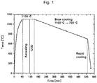
- the substrate was set inside the tubular furnace, and then the entire quartz tube was evacuated by a rotary pump. After that, hydrogen gas was flowed at 10 sccm to reach 40 to 50 Pa. While flowing the same amount of hydrogen gas, the temperature was raised to 1100°C over 60 minutes, and the temperature of 1100°C was retained for 60 minutes, as shown in Fig. 1 . In this way, the crystallinity of the metal catalyst that had been film formed by sputtering was increased, and further the smoothness of the surface was improved. In addition, a natural oxide film on a surface of the metal can be removed by hydrogen gas.
- borazine (B 3 N 3 H 6 ) was used as a raw material for the boron and the nitrogen. Liquid borazine was placed in a bottle with hydrogen of 0.12 to 0.13 MPa while cooling at -10°C. A hydrogen gas at 0.27 sccm containing a borazine vaporized gas from the bottle was mixed with a hydrogen gas at 10 sccm of the main line, and the mixture was introduced into the tubular furnace. This reaction was performed for 30 minutes.
- the cooling rate was controlled at 1 °C/min, and the cooling was performed until the temperature reached 700°C. After the temperature reached 700°C, the tubular furnace was turned off and cooled to room temperature.
- the substrate was taken out.
- the h-BN formed on a metal film was transferred onto a SiO 2 /Si substrate.
- the amount and the thickness distribution of the generated h-BN can be easily analyzed with an optical microscope. Further, the Raman peak obtained from the h-BN becomes strong after the transfer, and more accurate evaluation can be conducted.
- the transfer was typically performed by the following method.
- a polymethyl methacrylate (PMMA) solution was spin coated on a surface of the metal thin film after synthesis for protecting the h-BN, and the spin-coated PMMA film was baked at 115°C for 20 minutes.
- a thermal release tape (Revalpha manufactured by Nitto Denko Corporation) was deposited on the PMMA.
- a substrate was immersed into a mixed solution of a FeCl 3 aqueous solution and hydrochloric acid, a catalyst was sufficiently etched and the h-BN was floated to a surface of the solution together with the thermal tape and the PMMA, and then the floated one was picked up with a pair of tweezers.
- the FeCl 3 and the hydrochloric acid were carefully washed away from the picked-up one by using ion exchanged water, and then placed on a SiO 2 /Si substrate (having a thickness of SiO 2 of 300 nm) and dried at 60 to 100°C. After that, the heating was performed until the temperature reached 120°C, the adhesiveness of the thermal release tape was eliminated, the thermal release tape was removed from the PMMA film, and the PMMA film was removed in weakly heated acetone.
- Figs. 2(a)-2(e) show images at high magnification
- Figs. 3(a)-3(e) show images at low magnification.
- the uniformity of the thickness of the h-BN was improved as compared with that of the Fe alone ( Fig. 2(a) ). However, an area having a thick thickness was observed in some parts.
- the Ni was 70% ( Fig. 2(d) )
- a substantially uniform optical contrast was obtained, and it was indicated that the generated h-BN is extremely uniformly.
- the amount of generated h-BN was reduced due to the function of Ni.
- the h-BN having a large thickness was locally generated, and the h-BN of one to two layers having a thin thickness covered almost the entire surface of the Fe foil.
- the thickness of the h-BN shown in Fig. 2(d) was estimated by using a h-BN flake exfoliated from a single crystal.
- the height of the exfoliated h-BN flake was determined by an atomic force microscope (Nanoscope V manufactured by Bruker Corporation), and the optical contrast was measured by an optical microscope.
- the thickness of the h-BN shown in Fig. 2(d) was estimated to be approximately 3 to 10 nm.
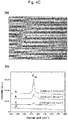
- Figs. 4A(a)-4A(d) , 4B(a)-4B(d) , 4C(a) and 4C(b) show optical microscope images and measurement results of the Raman spectrum of the h-BN transferred onto SiO 2 /Si substrates.
- Nanofinder 30 manufactured by Tokyo Instruments, Inc. was used, and the excitation wavelength was set to 532 nm, and the spot size was set to around 0.6 ⁇ m.
- Figs. 4A(a)-4A(d) shows optical microscope images and Raman spectra of the h-BNs obtained with Fe/MgO (100) and Ni/MgO (100).
- FIGs. 4C(a) and 4C(b) show an optical microscope image and Raman spectra of the h-BN transferred from a Fe foil onto a SiO 2 /Si substrate.
- the positions at which the Raman spectrum was measured are shown. Further, in the Raman spectra, the position and the full width at half maximum (FWHM) of E 2g peak were described.
- the E 2g peak intensity are uniform inside the grain.
- Ni had a stable fcc structure from room temperature to high temperature, and a Ni (100) thin film epitaxially deposited on MgO (100) was also retained during CVD at high temperature.
- a crystal plane corresponding to the fcc (110) plane was obtained ( Figs. 7(c) and 7(d) ).
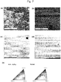
- Figs. 8(a)-8(e) show the results of observation of a surface of the transferred film of h-BN with an atomic force microscope (AFM).
- the h-BN generated on Fe/MgO (100) was relatively smooth, but at the edge of the h-BN, the upward warping of thin film grains was prominent ( Fig. 8(a) ).
- Almost no generation of h-BN occurred on Ni/MgO (100), and some flakes were observed in a small part ( Fig. 8(b) ).
- the h-BN transferred from Fe 0.7 -Ni 0.3 /MgO (100) (Ni 30%) had smooth surface, but multiple particles were also present ( Fig. 8(c) ).
- wrinkles were observed.
- the wrinkles were formed due to the difference between the thermal expansion coefficients of the metal thin film and the h-BN, or might have been introduced during transfer. Similar wrinkles were often observed before the transfer, and therefore, it is highly possible that wrinkles were generated mainly during the CVD.
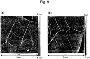
- h-BN after transfer onto a SiO 2 /Si substrate was analyzed with an optical microscope and an atomic force microscope (AFM).
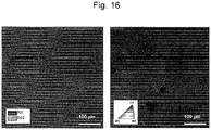
- Figs. 10(a) to 10(c) show optical microscope images (at low magnification and at high magnification) and an atomic force microscope image, of the synthesized h-BN, respectively. From these microscope images, it was confirmed that an extremely uniform h-BN thin film having a thickness of around 3 nm was obtained.
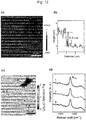
- Figs. 12(a)-12(d) show atomic force microscope images and measurement results of the Raman spectrum of the h-BN transferred onto a SiO 2 /Si substrate.
- Fig. 12(c) shows intensity mapping of the E 2g peak of the Raman spectrum in the same area as that of Fig. 12(a), and Fig. 12(d) shows Raman spectra at the positions with the numbers described in Fig. 12(c) .
- a film of a Ni metal was formed on a surface of a substrate by sputtering to prepare Ni/spinel (100) in a similar procedure as in Example 1 except that a spinel substrate having a (100) plane was used as the single crystal substrate.
- a h-BN thin film was synthesized by a CVD method under similar conditions as in Example 1 except that the Ni/spinel (100) substrate was used, and nitrogen gas was mixed at 50% with the hydrogen gas to be used in supplying a borazine vaporized gas as a raw material and in performing the cooling, and the generated h-BN was transferred onto a SiO 2 /Si substrate in a similar manner as in Example 1.
- the full width at half maximum of the E 2g peak derived from the h-BN was in a range of 15 to 20 cm -1 , and it was confirmed that the crystallinity is high.
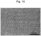
- the h-BN after transfer onto a SiO 2 /Si substrate was analyzed with an optical microscope. As shown in Fig. 15 , a microscope image having a substantially uniform optical contrast was obtained, and it was confirmed that the h-BN having high crystallinity was generated.
- Fig. 17(a) shows the average (MEAN), the standard deviation (SD), the coefficient of variation (CV(%)) of each of the G component intensities.
- the peak observed in the vicinity of the G value of 170 to 185 is a peak derived from the oxide (SiO 2 ) of the Si substrate.
- a h-BN thin film was synthesized by a CVD method under similar conditions as in Example 1, and the generated h-BN was transferred onto a SiO 2 /Si substrate in a similar manner as in Example 1.
- nitrogen gas was mixed at 25% with the hydrogen gas to be used in supplying a borazine vaporized gas as a raw material and in performing the cooling.
- the formation amount of the h-BN thin film was higher at a cooling rate of 1°C/min than that at a cooling rate of 2.5°C/min. From these results, it is suggested that the cooling rate in CVD is one of the factors that significantly affect the h-BN generation amount, and as the cooling rate is slower, the more uniform and larger h-BN thin film can be obtained.
- a h-BN thin film was synthesized by a CVD method.
- a h-BN thin film was synthesized by a CVD method under similar conditions as in Example 1 except that the cooling rate in CVD was changed to 5°C/min. The results are shown in Figs. 19(a)-19(c) .
- a h-BN thin film was synthesized by a CVD method under similar conditions as in Example 1 except that the cooling rate in CVD was changed to 1°C/min. The results are shown in Figs. 20(a)-20(c) .
- a h-BN thin film was synthesized by a CVD method under similar conditions as in Example 1 except that super invar was used, and the cooling rate from the synthesis temperature in CVD to 700°C was changed to the following four different ways of (i) to (iv):
- Figs. 21(a) to 21(d) From the optical microscope images shown in Figs. 21(a) to 21(d) , as the cooling rate from the synthesis temperature was decreased to 5°C/min, 1 °C/min, 0.5°C/min, and 0.25°C/min, a h-BN thin film having more excellent uniformity was observed. This suggests that the cooling rate in a temperature range close to the synthesis temperature in an initial stage of the cooling process leads to the increase in the h-BN amount and to the formation of a more uniform and larger h-BN thin film. In particular, Fig. 21(d) shows that the uniformity of the h-BN was extremely improved, and the h-BN having high quality was able to be synthesized.
- Figs. 22(a) and 22(b) show measurement results of the Raman spectrum of the h-BN synthesized under the condition of the above-described (ii).
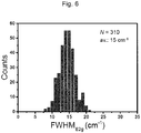
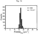
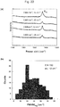
- the E 2g peaks derived from the h-BN were confirmed at 1368 to 1369 cm -1 , and it can be understood that the crystallinity was favorable from the values of the full width at half maximum.
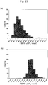
- 150 places were randomly selected from a 20- ⁇ m square area of the h-BN, and the intensity and the full width at half maximum (FWHM) of the E 2g peak derived from the h-BN were measured.
- FWHM full width at half maximum
- a h-BN thin film was synthesized by using the super invar used in Example 5-1 and by changing the temperature profile of the CVD synthesis. Specifically, the temperature was raised to 1100°C in 60 minutes, and the temperature of 1100°C was retained for 40 minutes as shown in Fig. 1 , and then the temperature was raised to 1150°C over 20 minutes, and the CVD reaction was performed at the temperature for 30 minutes in a similar procedure as in Example 1. After that, the cooling was performed at a rate of 5°C/min until the temperature reached 700°C, and after the temperature reached 700°C, the tubular furnace was turned off and cooled to room temperature.
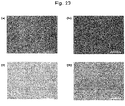
- Figs. 23(a)-23(d) show optical microscope images of the h-BN after transferred onto a SiO 2 /Si substrate.
- Figs. 23(a) and 23(c) show images at high magnification and at low magnification of the h-BN synthesized under the condition of (i) in Example 5-1
- Figs. 23(b) and 23(d) show images at high magnification and at low magnification of the h-BN synthesized in the present Example. From the images shown in Figs.
- WO 3 and sulfur powder were used as raw materials, the temperature was independently controlled to sublime the materials, and the substrate was heated to 800°C to grow the crystals.
- Fig. 24(a) shows an atomic force microscope image of the WS 2 grown on h-BN. It can be understood from the triangular shape that the WS 2 was thin and grew as small single crystals.
- WS 2 was allowed to grow also on SiO 2 /Si under the same conditions, and then each of the fluorescence spectra of the WS 2 on h-BN and the WS 2 on SiO 2 was measured.
- Nanofinder 30 described above was used, and the wavelength of the excitation light was also set to 532 nm.
- Fig. 24(b) shows the results of the fluorescence spectra. It can be understood that the peak intensity of the WS 2 grown on h-BN is strong and 46 times stronger than that of the WS 2 grown on SiO 2 . Further, it can be understood that the line width of photoluminescence (PL) of the WS 2 on h-BN is extremely narrow from 72 meV on SiO 2 to 24 meV on h-BN.
- Figs. 25(a) and 25(b) show histograms of the full width at half maximum of the fluorescence spectra shown in Fig. 24(b) . From the histograms shown in Figs. 25(a) and 25(b) , it is quantitatively understood that the line width of PL of the WS 2 on h-BN is narrower than that of the WS 2 grown on SiO 2 . The increase in the intensity of fluorescence and the sharpening in the peak in the WS 2 are indicated that with the h-BN thin film synthesized in the present Example, influences of the surface roughness of the SiO 2 substrate, the charge impurities, the optical phonon, and the like can be well screened. Figs.
- 26(a) and 26(b) show scatter plot graphs obtained by adding the information of the peak positions in the fluorescence spectra of Fig. 24(b) to the information of the histograms of Figs. 25(a) and 25(b) .
- the scatter plot graphs shown in Figs. 26(a) and 26(b) it is indicated that as the peak position of the fluorescence spectrum shifts to the lower energy side, the influence of charge impurities on the SiO 2 substrate is increased. More specifically, the fluorescence from excitons is in the vicinity of 2.01 eV, and the fluorescence from the negative trion derived from the negative charge on the SiO 2 surface is mixed in the vicinity of 1.98 eV.
- the h-BN thin film produced according to the present invention has an advantage of increasing the area by a CVD method, and further can be applied with excellent properties as a substrate material for various atomic layered materials.
- a single layer graphene film formed by a CVD method was transferred onto each of the h-BN synthesized by using super invar of a metal foil and the SiO 2 /Si, and the properties of the graphene were analyzed by a Raman spectrum.
- the single layer graphene film was formed on Cu (111) on a sapphire substrate by a CVD method, and then a polymethyl methacrylate (PMMA) solution was spin coated on a surface of the single layer graphene film, and one obtained by removing Cu by etching was transferred onto the h-BN or the SiO 2 /Si.
- PMMA polymethyl methacrylate
- the full width at half maximum (26 cm -1 ) of the 2D band of the graphene on the h-BN (spectrum on the upper side) is narrower than the full width at half maximum (34 cm -1 ) of the graphene (spectrum on the lower side) on the SiO 2 /Si, and it can be understood that the influence from the SiO 2 is significantly decreased by the h-BN.
- the full width at half maximum (26 cm -1 ) of the 2D band of the graphene on the h-BN has a value almost the same degree with the value previously reported for the graphene on the h-BN exfoliated from a bulk single crystal, and thus it is indicated that the h-BN of the present invention has a screening effect almost the same degree as that of exfoliated one.
- Figs. 28(a) and 28(b) show histograms each showing the distribution of the full width at half maximum (FWHM) of the 2D band in multiple measurement points for each of the graphene on the h-BN and the graphene on the SiO 2 /Si.
- the h-BN thin film synthesized by a CVD method according to the present invention it was confirmed from multiple measurement points that the characteristics inherent in graphene can be exhibited more efficiently and effectively by using h-BN.
- the hexagonal boron nitride thin film according to the present invention has the characteristics that the area is large, the thickness is uniform, and the crystallinity is high, and therefore can be used for a variety of electronic devices including a semiconductor device.
Landscapes
- Chemical & Material Sciences (AREA)
- Engineering & Computer Science (AREA)
- Organic Chemistry (AREA)
- Materials Engineering (AREA)
- Metallurgy (AREA)
- Chemical Kinetics & Catalysis (AREA)
- Mechanical Engineering (AREA)
- General Chemical & Material Sciences (AREA)
- Inorganic Chemistry (AREA)
- Ceramic Engineering (AREA)
- Manufacturing & Machinery (AREA)
- Structural Engineering (AREA)
- Crystallography & Structural Chemistry (AREA)
- Chemical Vapour Deposition (AREA)
- Thin Film Transistor (AREA)
- Compositions Of Oxide Ceramics (AREA)
- Crystals, And After-Treatments Of Crystals (AREA)
Applications Claiming Priority (2)
| Application Number | Priority Date | Filing Date | Title |
|---|---|---|---|
| JP2017001291 | 2017-01-06 | ||
| PCT/JP2018/000107 WO2018128193A1 (ja) | 2017-01-06 | 2018-01-05 | 六方晶窒化ホウ素薄膜とその製造方法 |
Publications (2)
| Publication Number | Publication Date |
|---|---|
| EP3567005A1 true EP3567005A1 (de) | 2019-11-13 |
| EP3567005A4 EP3567005A4 (de) | 2020-07-29 |
Family
ID=62791115
Family Applications (1)
| Application Number | Title | Priority Date | Filing Date |
|---|---|---|---|
| EP18735883.3A Pending EP3567005A4 (de) | 2017-01-06 | 2018-01-05 | Hexagonale bornitrid-dünnschicht und verfahren zur herstellung davon |
Country Status (6)
| Country | Link |
|---|---|
| US (1) | US11352692B2 (de) |
| EP (1) | EP3567005A4 (de) |
| JP (1) | JP7136453B2 (de) |
| KR (1) | KR102444656B1 (de) |
| CN (1) | CN110167876B (de) |
| WO (1) | WO2018128193A1 (de) |
Families Citing this family (13)
| Publication number | Priority date | Publication date | Assignee | Title |
|---|---|---|---|---|
| CN110921637B (zh) | 2018-09-20 | 2022-09-23 | 中国科学院上海微系统与信息技术研究所 | 多层六方氮化硼薄膜的制备方法 |
| JP7253943B2 (ja) * | 2019-03-15 | 2023-04-07 | 東京エレクトロン株式会社 | 六方晶窒化ホウ素膜を形成する方法および装置 |
| TWI732544B (zh) * | 2020-05-05 | 2021-07-01 | 國立中正大學 | 二維材料薄膜檢測方法及二維材料薄膜檢測系統 |
| KR20220141651A (ko) * | 2021-04-13 | 2022-10-20 | 삼성전자주식회사 | 전계 효과 트랜지스터 구조체 |
| US12230680B2 (en) * | 2021-08-30 | 2025-02-18 | Taiwan Semiconductor Manufacturing Company, Ltd. | Manufacturing method of semiconductor device including hBNC layer, and manufacturing method of HBNC layer |
| CN116262985A (zh) * | 2021-12-14 | 2023-06-16 | 中国科学院半导体研究所 | 二维原子晶体及其生长方法 |
| JPWO2023189258A1 (de) * | 2022-03-31 | 2023-10-05 | ||
| KR102904067B1 (ko) * | 2022-05-23 | 2025-12-24 | 주식회사 넥스티리얼즈 | 다층 단결정 육방정계 질화붕소 박막 및 이의 제조방법 |
| KR102758627B1 (ko) | 2022-07-01 | 2025-01-22 | 경기대학교 산학협력단 | 질화붕소의 제조방법 |
| CN115613130B (zh) * | 2022-08-29 | 2024-06-04 | 海南大学 | 一种在常压下化学气相沉积制备六方氮化硼薄膜的方法 |
| CN115261978B (zh) * | 2022-08-29 | 2023-08-04 | 东南大学 | 一种制备具有铁电性的ab堆垛的多层氮化硼薄膜的方法 |
| CN116396083B (zh) * | 2023-03-28 | 2024-01-30 | 南京工业大学 | 一种大面积六方氮化硼薄膜的快速制备方法 |
| CN121471813A (zh) * | 2026-01-06 | 2026-02-06 | 湖北凯力专用汽车有限公司 | 一种防水隔热一体化压缩垃圾车封闭舱涂层及其制备方法 |
Family Cites Families (18)
| Publication number | Priority date | Publication date | Assignee | Title |
|---|---|---|---|---|
| JP5553353B2 (ja) | 2008-03-26 | 2014-07-16 | 学校法人早稲田大学 | 単原子膜の製造方法 |
| US8436404B2 (en) * | 2009-12-30 | 2013-05-07 | Intel Corporation | Self-aligned contacts |
| WO2011127258A1 (en) | 2010-04-07 | 2011-10-13 | Massachusetts Institute Of Technology | Fabrication of large-area hexagonal boron nitride thin films |
| JP5105028B2 (ja) | 2010-11-24 | 2012-12-19 | 富士電機株式会社 | グラフェンを含む導電性薄膜および透明導電膜 |
| JP2013067549A (ja) | 2011-09-06 | 2013-04-18 | Waseda Univ | 薄膜の形成方法 |
| US8884310B2 (en) | 2011-10-19 | 2014-11-11 | Sunedison Semiconductor Limited (Uen201334164H) | Direct formation of graphene on semiconductor substrates |
| KR101878746B1 (ko) * | 2011-12-06 | 2018-07-17 | 삼성전자주식회사 | 육방정계 질화붕소 시트, 그의 제조방법 및 이를 구비하는 전기소자 |
| CN103663416B (zh) * | 2012-09-01 | 2015-09-09 | 董国材 | 一种制备石墨烯和单层六角氮化硼复合材料的方法 |
| KR101917743B1 (ko) * | 2012-10-24 | 2018-11-12 | 삼성전자주식회사 | 육방정계 질화붕소 시트, 그의 제조방법 및 이를 구비하는 전기소자 |
| CN103031516B (zh) * | 2013-01-18 | 2014-12-17 | 浙江大学 | 一种六角相氮化硼薄膜的制备方法 |
| KR20140114199A (ko) | 2013-03-18 | 2014-09-26 | 삼성전자주식회사 | 이종 적층 구조체 및 그 제조방법, 및 상기 이종 적층 구조체를 구비하는 전기소자 |
| KR102100925B1 (ko) | 2013-03-22 | 2020-04-14 | 삼성전자주식회사 | 기판 구조체, 상기 기판 구조체를 형성하는 방법, 및 이를 구비하는 전기소자 |
| ES2968152T3 (es) | 2013-05-09 | 2024-05-08 | Globalwafers Co Ltd | Formación directa y secuencial de monocapas de nitruro de boro y grafeno sobre sustratos |
| CN103774113B (zh) | 2014-02-24 | 2015-10-28 | 中国科学院上海微系统与信息技术研究所 | 一种制备六方氮化硼薄膜的方法 |
| CN104233222B (zh) * | 2014-09-26 | 2016-06-29 | 厦门大学 | 一种直接在Si衬底上生长六方氮化硼二维薄膜的方法 |
| KR102395774B1 (ko) * | 2015-02-12 | 2022-05-09 | 삼성전자주식회사 | 이음매 없는 육방정계 질화붕소 원자모노층 박막 및 그 제조방법 |
| KR101685100B1 (ko) * | 2015-03-27 | 2016-12-09 | 한국과학기술연구원 | 기재 위에 h-BN 후막을 형성하는 방법 및 그로부터 제조된 h-BN 후막 적층체 |
| CN105568253B (zh) * | 2016-01-06 | 2018-12-11 | 复旦大学 | 一种等离子体化学气相沉积设备生长六方氮化硼的方法 |
-
2018
- 2018-01-05 US US16/475,498 patent/US11352692B2/en active Active
- 2018-01-05 KR KR1020197017101A patent/KR102444656B1/ko active Active
- 2018-01-05 EP EP18735883.3A patent/EP3567005A4/de active Pending
- 2018-01-05 JP JP2018560410A patent/JP7136453B2/ja active Active
- 2018-01-05 CN CN201880006202.3A patent/CN110167876B/zh active Active
- 2018-01-05 WO PCT/JP2018/000107 patent/WO2018128193A1/ja not_active Ceased
Also Published As
| Publication number | Publication date |
|---|---|
| KR102444656B1 (ko) | 2022-09-19 |
| JPWO2018128193A1 (ja) | 2019-11-07 |
| CN110167876B (zh) | 2022-08-30 |
| EP3567005A4 (de) | 2020-07-29 |
| KR20190100915A (ko) | 2019-08-29 |
| CN110167876A (zh) | 2019-08-23 |
| JP7136453B2 (ja) | 2022-09-13 |
| WO2018128193A1 (ja) | 2018-07-12 |
| US20190345603A1 (en) | 2019-11-14 |
| US11352692B2 (en) | 2022-06-07 |
Similar Documents
| Publication | Publication Date | Title |
|---|---|---|
| US11352692B2 (en) | Hexagonal boron nitride thin film and method for producing the same | |
| Suzuki et al. | Growth of atomically thin hexagonal boron nitride films by diffusion through a metal film and precipitation | |
| KR101467118B1 (ko) | 스퍼터링 방법을 이용한 산화갈륨 나노와이어의 제조 방법 | |
| Miller et al. | Giant secondary grain growth in Cu films on sapphire | |
| CN110921637A (zh) | 多层六方氮化硼薄膜的制备方法 | |
| CN111206283B (zh) | 一种二硒化铬二维材料的制备和应用 | |
| Lee et al. | Effect of nucleation density on the crystallinity of graphene grown from mobile hot-wire-assisted CVD | |
| Mukherjee et al. | A comparative study of nanocrystalline Cu film deposited using anodic vacuum arc and dc magnetron sputtering | |
| Nath et al. | Investigation of dilute ferromagnetism induced at room temperature in undoped crystalline AlN thin film after isothermal annealing in a controlled oxygen environment | |
| Jauberteau et al. | A reduction–nitridation process of molybdenum films in expanding microwave plasma: Crystal structure of molybdenum nitrides | |
| Bui et al. | Thin films of Co 1.7 Fe 1.3 O 4 prepared by radio frequency sputtering–the first step towards their spinodal decomposition | |
| Nam et al. | Abnormal grain growth for single-crystal Cu substrate and chemical vapor deposition of graphene on it | |
| Murakawa et al. | Optical properties of cubic boron nitride films made by a reactive ion plating method | |
| KR102672480B1 (ko) | 도핑 그래핀의 제조 방법 및 이에 의해 제조된 도핑 그래핀 | |
| Tang et al. | Role of high microwave power on growth and microstructure of thick nanocrystalline diamond films: A comparison with large grain polycrystalline diamond films | |
| US20210332469A1 (en) | Method for manufacturing two-dimensional material | |
| JP6589098B2 (ja) | 他元素含有蒸発源、dlc膜形成方法及びdlc膜形成装置 | |
| Kumar et al. | Structural, morphological and electronic properties of pulsed laser grown Eu2O3 thin films | |
| US11823895B2 (en) | Methods and devices for graphene formation on flexible substrates by plasma-enhanced chemical vapor deposition | |
| Hossain et al. | Large-area, thermally-sulfurized WS2 thin films: control of growth direction and use as a substrate for GaN epitaxy | |
| US11859308B2 (en) | Single crystal transition metal dichalcogenide thin film and method for synthesizing the same | |
| KR101290340B1 (ko) | 알에프 스퍼터링방법을 이용한 그래핀 제작방법 | |
| Dasgupta et al. | Microstructure of thick chromium–nitride coating synthesized using plasma assisted MOCVD technique | |
| Kawasaki et al. | Structural investigation of Ru/Pt nanocomposite films prepared by plasma-enhanced atomic layer depositions | |
| Yang et al. | Chemical vapor deposition of large-area ultrathin Cr3Te4 nanosheets with robust ferromagnetism |
Legal Events
| Date | Code | Title | Description |
|---|---|---|---|
| STAA | Information on the status of an ep patent application or granted ep patent |
Free format text: STATUS: THE INTERNATIONAL PUBLICATION HAS BEEN MADE |
|
| PUAI | Public reference made under article 153(3) epc to a published international application that has entered the european phase |
Free format text: ORIGINAL CODE: 0009012 |
|
| STAA | Information on the status of an ep patent application or granted ep patent |
Free format text: STATUS: REQUEST FOR EXAMINATION WAS MADE |
|
| 17P | Request for examination filed |
Effective date: 20190702 |
|
| AK | Designated contracting states |
Kind code of ref document: A1 Designated state(s): AL AT BE BG CH CY CZ DE DK EE ES FI FR GB GR HR HU IE IS IT LI LT LU LV MC MK MT NL NO PL PT RO RS SE SI SK SM TR |
|
| AX | Request for extension of the european patent |
Extension state: BA ME |
|
| RIN1 | Information on inventor provided before grant (corrected) |
Inventor name: TANAKA DAICHI Inventor name: AGO HIROKI Inventor name: NAKANDAKARI SHO Inventor name: KAWAHARA KENJI Inventor name: UCHIDA YUKI |
|
| DAV | Request for validation of the european patent (deleted) | ||
| DAX | Request for extension of the european patent (deleted) | ||
| A4 | Supplementary search report drawn up and despatched |
Effective date: 20200629 |
|
| RIC1 | Information provided on ipc code assigned before grant |
Ipc: C23C 16/34 20060101ALI20200623BHEP Ipc: C23C 16/38 20060101ALI20200623BHEP Ipc: H01L 21/336 20060101ALI20200623BHEP Ipc: C01B 21/064 20060101AFI20200623BHEP Ipc: H01L 29/786 20060101ALI20200623BHEP Ipc: B32B 9/00 20060101ALI20200623BHEP |
|
| STAA | Information on the status of an ep patent application or granted ep patent |
Free format text: STATUS: EXAMINATION IS IN PROGRESS |
|
| 17Q | First examination report despatched |
Effective date: 20240618 |
|
| 17Q | First examination report despatched |
Effective date: 20240626 |