EP3568721B1 - Appareil et procédé de couplage de lumière - Google Patents
Appareil et procédé de couplage de lumière Download PDFInfo
- Publication number
- EP3568721B1 EP3568721B1 EP17701070.9A EP17701070A EP3568721B1 EP 3568721 B1 EP3568721 B1 EP 3568721B1 EP 17701070 A EP17701070 A EP 17701070A EP 3568721 B1 EP3568721 B1 EP 3568721B1
- Authority
- EP
- European Patent Office
- Prior art keywords
- waveguide element
- width
- optical coupler
- waveguide
- layer
- Prior art date
- Legal status (The legal status is an assumption and is not a legal conclusion. Google has not performed a legal analysis and makes no representation as to the accuracy of the status listed.)
- Active
Links
Images





Classifications
-
- G—PHYSICS
- G02—OPTICS
- G02B—OPTICAL ELEMENTS, SYSTEMS OR APPARATUS
- G02B6/00—Light guides; Structural details of arrangements comprising light guides and other optical elements, e.g. couplings
- G02B6/10—Light guides; Structural details of arrangements comprising light guides and other optical elements, e.g. couplings of the optical waveguide type
- G02B6/12—Light guides; Structural details of arrangements comprising light guides and other optical elements, e.g. couplings of the optical waveguide type of the integrated circuit kind
- G02B6/122—Basic optical elements, e.g. light-guiding paths
- G02B6/1228—Tapered waveguides, e.g. integrated spot-size transformers
-
- G—PHYSICS
- G02—OPTICS
- G02B—OPTICAL ELEMENTS, SYSTEMS OR APPARATUS
- G02B6/00—Light guides; Structural details of arrangements comprising light guides and other optical elements, e.g. couplings
- G02B6/24—Coupling light guides
- G02B6/26—Optical coupling means
- G02B6/30—Optical coupling means for use between fibre and thin-film device
- G02B6/305—Optical coupling means for use between fibre and thin-film device and having an integrated mode-size expanding section, e.g. tapered waveguide
-
- G—PHYSICS
- G02—OPTICS
- G02B—OPTICAL ELEMENTS, SYSTEMS OR APPARATUS
- G02B6/00—Light guides; Structural details of arrangements comprising light guides and other optical elements, e.g. couplings
- G02B6/10—Light guides; Structural details of arrangements comprising light guides and other optical elements, e.g. couplings of the optical waveguide type
- G02B6/12—Light guides; Structural details of arrangements comprising light guides and other optical elements, e.g. couplings of the optical waveguide type of the integrated circuit kind
-
- G—PHYSICS
- G02—OPTICS
- G02B—OPTICAL ELEMENTS, SYSTEMS OR APPARATUS
- G02B6/00—Light guides; Structural details of arrangements comprising light guides and other optical elements, e.g. couplings
- G02B6/10—Light guides; Structural details of arrangements comprising light guides and other optical elements, e.g. couplings of the optical waveguide type
- G02B6/12—Light guides; Structural details of arrangements comprising light guides and other optical elements, e.g. couplings of the optical waveguide type of the integrated circuit kind
- G02B6/12002—Three-dimensional structures
-
- G—PHYSICS
- G02—OPTICS
- G02B—OPTICAL ELEMENTS, SYSTEMS OR APPARATUS
- G02B6/00—Light guides; Structural details of arrangements comprising light guides and other optical elements, e.g. couplings
- G02B6/10—Light guides; Structural details of arrangements comprising light guides and other optical elements, e.g. couplings of the optical waveguide type
- G02B6/12—Light guides; Structural details of arrangements comprising light guides and other optical elements, e.g. couplings of the optical waveguide type of the integrated circuit kind
- G02B6/12004—Combinations of two or more optical elements
-
- G—PHYSICS
- G02—OPTICS
- G02B—OPTICAL ELEMENTS, SYSTEMS OR APPARATUS
- G02B6/00—Light guides; Structural details of arrangements comprising light guides and other optical elements, e.g. couplings
- G02B6/24—Coupling light guides
- G02B6/42—Coupling light guides with opto-electronic elements
- G02B6/4201—Packages, e.g. shape, construction, internal or external details
- G02B6/4202—Packages, e.g. shape, construction, internal or external details for coupling an active element with fibres without intermediate optical elements, e.g. fibres with plane ends, fibres with shaped ends, bundles
-
- G—PHYSICS
- G02—OPTICS
- G02B—OPTICAL ELEMENTS, SYSTEMS OR APPARATUS
- G02B6/00—Light guides; Structural details of arrangements comprising light guides and other optical elements, e.g. couplings
- G02B6/10—Light guides; Structural details of arrangements comprising light guides and other optical elements, e.g. couplings of the optical waveguide type
- G02B6/12—Light guides; Structural details of arrangements comprising light guides and other optical elements, e.g. couplings of the optical waveguide type of the integrated circuit kind
- G02B2006/12035—Materials
- G02B2006/12038—Glass (SiO2 based materials)
-
- G—PHYSICS
- G02—OPTICS
- G02B—OPTICAL ELEMENTS, SYSTEMS OR APPARATUS
- G02B6/00—Light guides; Structural details of arrangements comprising light guides and other optical elements, e.g. couplings
- G02B6/10—Light guides; Structural details of arrangements comprising light guides and other optical elements, e.g. couplings of the optical waveguide type
- G02B6/12—Light guides; Structural details of arrangements comprising light guides and other optical elements, e.g. couplings of the optical waveguide type of the integrated circuit kind
- G02B2006/12035—Materials
- G02B2006/12061—Silicon
-
- G—PHYSICS
- G02—OPTICS
- G02B—OPTICAL ELEMENTS, SYSTEMS OR APPARATUS
- G02B6/00—Light guides; Structural details of arrangements comprising light guides and other optical elements, e.g. couplings
- G02B6/10—Light guides; Structural details of arrangements comprising light guides and other optical elements, e.g. couplings of the optical waveguide type
- G02B6/12—Light guides; Structural details of arrangements comprising light guides and other optical elements, e.g. couplings of the optical waveguide type of the integrated circuit kind
- G02B2006/12133—Functions
- G02B2006/12147—Coupler
-
- G—PHYSICS
- G02—OPTICS
- G02B—OPTICAL ELEMENTS, SYSTEMS OR APPARATUS
- G02B6/00—Light guides; Structural details of arrangements comprising light guides and other optical elements, e.g. couplings
- G02B6/10—Light guides; Structural details of arrangements comprising light guides and other optical elements, e.g. couplings of the optical waveguide type
- G02B6/12—Light guides; Structural details of arrangements comprising light guides and other optical elements, e.g. couplings of the optical waveguide type of the integrated circuit kind
- G02B2006/12133—Functions
- G02B2006/12152—Mode converter
-
- G—PHYSICS
- G02—OPTICS
- G02B—OPTICAL ELEMENTS, SYSTEMS OR APPARATUS
- G02B6/00—Light guides; Structural details of arrangements comprising light guides and other optical elements, e.g. couplings
- G02B6/10—Light guides; Structural details of arrangements comprising light guides and other optical elements, e.g. couplings of the optical waveguide type
- G02B6/12—Light guides; Structural details of arrangements comprising light guides and other optical elements, e.g. couplings of the optical waveguide type of the integrated circuit kind
- G02B2006/12166—Manufacturing methods
- G02B2006/12195—Tapering
-
- G—PHYSICS
- G02—OPTICS
- G02B—OPTICAL ELEMENTS, SYSTEMS OR APPARATUS
- G02B6/00—Light guides; Structural details of arrangements comprising light guides and other optical elements, e.g. couplings
- G02B6/10—Light guides; Structural details of arrangements comprising light guides and other optical elements, e.g. couplings of the optical waveguide type
- G02B6/12—Light guides; Structural details of arrangements comprising light guides and other optical elements, e.g. couplings of the optical waveguide type of the integrated circuit kind
- G02B6/122—Basic optical elements, e.g. light-guiding paths
- G02B6/1223—Basic optical elements, e.g. light-guiding paths high refractive index type, i.e. high-contrast waveguides
-
- G—PHYSICS
- G02—OPTICS
- G02B—OPTICAL ELEMENTS, SYSTEMS OR APPARATUS
- G02B6/00—Light guides; Structural details of arrangements comprising light guides and other optical elements, e.g. couplings
- G02B6/10—Light guides; Structural details of arrangements comprising light guides and other optical elements, e.g. couplings of the optical waveguide type
- G02B6/14—Mode converters
-
- G—PHYSICS
- G02—OPTICS
- G02B—OPTICAL ELEMENTS, SYSTEMS OR APPARATUS
- G02B6/00—Light guides; Structural details of arrangements comprising light guides and other optical elements, e.g. couplings
- G02B6/24—Coupling light guides
- G02B6/26—Optical coupling means
- G02B6/30—Optical coupling means for use between fibre and thin-film device
-
- G—PHYSICS
- G02—OPTICS
- G02B—OPTICAL ELEMENTS, SYSTEMS OR APPARATUS
- G02B6/00—Light guides; Structural details of arrangements comprising light guides and other optical elements, e.g. couplings
- G02B6/24—Coupling light guides
- G02B6/42—Coupling light guides with opto-electronic elements
Definitions
- the embodiments described herein relate to an apparatus and method for coupling light, and in particular to an optical coupler and a method of forming an optical coupler.
- US 2009/0297093 describes an optical coupler formed of a low index material and which exhibits a mode field diameter suitable to provide efficient coupling between a free space optical signal (of large mode field diameter) and a single mode high index waveguide formed on an optical substrate.
- One embodiment comprises an anti-resonant reflecting optical waveguide (ARROW) structure in conjunction with an embedded (high index) nanotaper coupling waveguide.
- ARROW anti-resonant reflecting optical waveguide
- PSoC photonic system on chip
- a SOA is made, for example, from so called Group III-V semiconductor materials, whereby Group III materials include for example Aluminium (Al), Gallium (Ga) and Indium (In), and whereby Group V materials include for example Nitride (N), Phosphide (P), Arsenide (As) and Antimony (Sb).
- Group III materials include for example Aluminium (Al), Gallium (Ga) and Indium (In)
- Group V materials include for example Nitride (N), Phosphide (P), Arsenide (As) and Antimony (Sb).
- a key aspect is the need of integrating dies with III-V active layers with a silicon chip.
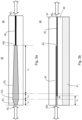
- FIG. 1 shows an example of a known SSC 10 based on a taper structure.
- the SSC of Figure 1 comprises a silicon optical waveguide 1 having an inverse taper.
- the silicon optical waveguide 1 is surrounded with a non-stoichiometric silica waveguide core 3 that is in turn surrounded by a silica cladding layer 5.
- This structure is formed on a BOX layer 7, which is in turn formed on a substrate 9 in silicon over insulator, SOI, wafers.
- the silicon optical waveguide 1 sits on top of the BOX layer 7, and is surrounded by the non-stoichiometric silica core 3, e.g. SiOx, which comprises more oxygen atoms in order to slightly increase the refractive index.
- the non-stoichiometric silica core 3 e.g. SiOx, which comprises more oxygen atoms in order to slightly increase the refractive index.
- FIG. 2 shows another example of a known SSC 20 based on a taper structure.
- This device comprises three tapered silicon waveguides 1a, 1b, 1c formed in the same layer and structured with the shape of a trident fork, surrounded by a silica cladding layer 5.
- the structure is formed on a BOX layer 7, which is in turn formed on a substrate 9 in SOI wafers.
- US 2009/297093 A1 discloses a silicon-based optical coupler that is formed of a low index optical waveguide of material having a lower refractive index than a single mode optical waveguide, and a nanotaper coupling waveguide having a greater refractive index than the low index optical waveguide.
- US 2015/316720 A1 discloses a mode converter comprising a substrate, a silicon waveguide and a low-index waveguide.
- US 2011/116741 A1 discloses an optical mode transformer for efficiently coupling a single mode optical fiber to a high index contrast waveguide.
- an optical coupler comprising a substrate, and a first waveguide element provided in a first layer with respect to the substrate.
- the first waveguide element comprises a first end and a second end, and wherein the first end of the first waveguide element is coupled to input/output light to/from a first end of the optical coupler.
- the optical coupler comprises a second waveguide element provided in a second layer, the second layer arranged adjacent to the first layer, wherein the second waveguide element comprises a first end and a second end, and wherein the first end of the second waveguide element is coupled to input/output light to/from a second end of the optical coupler.
- the first waveguide element is configured to extend from the first end of the optical coupler towards the second end of the optical coupler
- the second waveguide element is configured to extend from the second end of the optical coupler towards the first end of the optical coupler, such that the first waveguide element overlaps with the second waveguide element to adapt light passing between the first end of the first waveguide element and first end of the second waveguide element.
- a semiconductor photonic device comprising a first optical module, a second optical module, and an optical coupler as defined above, or any of the other embodiments herein, for coupling light between the first optical module and the second optical module.
- a method of forming an optical coupler comprises providing a substrate, and forming a first waveguide element in a first layer with respect to the substrate, wherein the first waveguide element comprises a first end and a second end, and wherein the first end of the first waveguide element is coupled to input/output light to/from a first end of the optical coupler.
- the method comprises forming a second waveguide element in a second layer, the second layer formed adjacent to the first layer, wherein the second waveguide element comprises a first end and a second end, and wherein the first end of the second waveguide element is coupled to input/output light to/from a second end of the optical coupler.
- the first waveguide element is formed to extend from the first end of the optical coupler towards the second end of the optical coupler, and wherein the second waveguide element is formed to extend from the second end of the optical coupler towards the first end of the optical coupler, such that the first waveguide element overlaps with the second waveguide element to adapt light passing between the first end of the first waveguide element and first end of the second waveguide element.
- optical couplers for interfacing between first and second light modules, for example for use as spot size converters, for example when interfacing between a first die (such as a Group III-V active die, for example a semiconductor optical amplifier, SOA) and a second die (such as a silicon waveguide in a silicon-on-insulator SOI wafer, for example coupled to a laser). It is noted, however, that the optical couplers described herein may be used for other applications.
- a first die such as a Group III-V active die, for example a semiconductor optical amplifier, SOA
- SOA semiconductor optical amplifier
- SOI wafer silicon-on-insulator SOI wafer
- Figures 3a, 3b and 3c show top, side cross-section and bottom views respectively of an optical coupler 40 according to a first embodiment.
- the optical coupler 40 comprises a substrate 41.
- a first waveguide element 45 is provided in a first layer with respect to the substrate 41, wherein the first waveguide element 45 comprises a first end 45a and a second end 45b.
- the first end 45a of the first waveguide element 45 is coupled to input/output light to/from a first end of the optical coupler, for example the end of the optical coupler to the right of the page, which may be coupled for example to a light module, such as a silicon waveguide on a SOI wafer.
- the first waveguide element 45 may be physically coupled, or form an integral part, of a waveguide which the first waveguide element 45 interfaces with.
- the optical coupler 40 of Figure 3b comprises a second waveguide element 43 provided in a second layer, the second layer arranged adjacent to the first layer, wherein the second waveguide element 43 comprises a first end 43a and a second end 43b.
- the first end 43a of the second waveguide element 43 is coupled to input/output light to/from a second end of the optical coupler, for example the end of the optical coupler to the left of the page, which may be coupled for example to a light module, such as a semiconductor optical amplifier, SOA.
- the first waveguide element 45 is configured to extend from the first end of the optical coupler towards the second end of the optical coupler
- the second waveguide element 43 is configured to extend from the second end of the optical coupler towards the first end of the optical coupler, such that the first waveguide element 45 overlaps with the second waveguide element 43 to adapt light passing between the first end 45a of the first waveguide element 45 and first end 43a of the second waveguide element 43.
- the first waveguide element 45 overlaps with the second waveguide element 43 in a direction parallel to a plane of the substrate 41, but in separate layers, e.g. as shown in Figure 3b .
- the first waveguide element 45 also overlaps with the second waveguide element 43 in a direction perpendicular to a plane of the substrate 41, but in separate layers, e.g. as shown in Figure 3a .
- the configuration of the optical coupler adapts light passing between the first end 45a of the first waveguide element 45 and first end 43a of the second waveguide element 43. Therefore, light from a light source, for example an external light source, coupled to the first end 43a of the second waveguide element 43 is adapted as it passes through the second waveguide element 43 and the first waveguide element 45 towards the first end 45a of the first waveguide element 45.
- the second waveguide element 43 and first waveguide element 45 are configured to adapt a mode shape (for example spot size) of an external light source coupled thereto, for example from a SOA.
- the second waveguide element 43 comprises an expansion region 43 1 , a constant width region 43 2 (which may be optional, as described later in Figures 4a to 4c ) and a compression region 43 3 .
- the expansion region 43 1 comprises an increasing width from a third width at the first end 43a of the second waveguide element 43 to a larger, fourth width, at an interface with the constant width region 43 2 .
- the constant width region 43 2 comprises the fourth width between the expansion region 43 1 and the compression region 43 3 .
- the compression region 43 3 tapers in width from the fourth width to having a smaller, fifth width, at the second end 43b of the second waveguide element 43.
- the first waveguide element 45 guides the light out of the right side of the optical coupler, i.e. via its first end 45a. This may comprise coupling light to a waveguide, including for example a SOI waveguide.
- such a SOI waveguide may be physically coupled to the first waveguide element 45 (for example forming a monolithically integral part thereof), for example where the optical coupler is integrally fabricated as part of a larger semiconductor photonic device comprising the SOI waveguide, for example as described later in Figure 5 .
- the optical coupler is configured to adapt light in the reverse direction, for light received at the right side of the optical coupler (i.e. first end of the optical coupler, i.e. at the first end 45a of the first waveguide element 45) and coupled to the left side of the optical coupler (i.e. second end of the optical coupler, i.e. the first end 43a of the second waveguide element 43).
- an aspect ratio of the first end 43a of the second waveguide element 43 is less than one, or in some examples substantially less than one.
- the aspect ratio may be less than 0.05.
- the aspect ratio may be defined as the ratio of the height of the waveguide element to the width of the waveguide element, wherein the height (or depth) is the thickness of the waveguide element perpendicular to the plane of the substrate, i.e. up-down direction in Figure 3b , and wherein the width is the distance perpendicular to the long axis of the waveguide element, i.e. up-down direction in Figure 3a .
- the height (or depth) of the waveguide element is less than, or substantially less than, its width.
- the aspect ratio would be 0.02, i.e. an aspect ratio of less than 0.05 as indicated above.
- a numerical aperture of the first end 43a of the second waveguide element 43 may be configured to match the numerical aperture of a light source, for example substantially match, or exactly match an external light source, coupled thereto. Optimal coupling may be achieved when the numerical aperture of the first end 43a of the second waveguide 43 matches the numerical aperture, for example both on the horizontal axis and on the vertical axis, of an input light mode from a light source coupled thereto.
- the optical coupler 40 is configured with the first waveguide element 45 and the second waveguide element 43 in overlap in adjacent layers. This enables light to pass via evanescent-coupling between the two layers, hence enabling light to be coupled through the optical coupler, i.e. between the respective first and second ends of the optical coupler.
- the optical coupler can be used, for example, as a spot size converter, SSC, for example to butt-couple between first and second modules that use light having different beam spot sizes.
- the first waveguide element 45 tapers in width from having a first width at its first end 45a to having a second width at its second end 45b.
- the width of the first waveguide element 45 tapers, e.g. uniformly, from the first width at its first end 45a to a point at its second end 45b.
- the term "width" in the context of the first waveguide element 45 refers to the width of the first waveguide element 45 in the plane of the layer used to form the first waveguide element. The same applies to the term "width" with respect to the second waveguide element 43, as described below.
- the optical coupler comprises a third layer 49 interposed between the first waveguide element 45 and the substrate 41, which is best illustrated in the cross-sectional view of Figure 3b .
- the third layer 49 comprises a material to help prevent optical signals from entering the substrate 41, and may comprise for example a buried oxide, BOX, layer 49. It is noted, however, that this layer is optional, and may be omitted in some examples, for example as illustrated in the cross-sectional view of Figure 3d (which shows an optical coupler similar to that of Figure 3b without a BOX layer 49).
- the substrate 41 could comprise a material with a refractive index lower than silicon, avoiding the need for a BOX layer.
- the substrate 41 and BOX layer 49 may form a silicon on insulator, SOI, wafer.
- the BOX layer 49 may comprise, for example, silicon dioxide.
- the technology used for silicon photonics may be based on SOI wafers that are produced with a BOX layer between a thin silicon layer (in which the optical circuits are formed) and the thick silicon substrate, with the purpose to avoid optical leakage in the silicon substrate. It is noted that a plurality of other layers may be provided between the substrate and the first waveguide element 45, for example to help with etching processes, and/or to help with positioning the first and second waveguides at the appropriate height for a particular application.
- the embodiments described herein may comprise a layer (not shown) between the first waveguide element 45 and the second waveguide element 43, such that the first waveguide element 45 and second waveguide element are not directly adjacent one another, i.e. not in immediately adjacent layers, but adjacent layers separated by another thin layer.
- the first waveguide element 45 and the second waveguide element 43 may be separated by a thin layer of material, for example silicon dioxide (SiO 2 ), providing a separation of between 0 to 1 ⁇ m, for example 70nm, between the first waveguide element 45 and the second waveguide element 43.
- a layer may be provided in some technological processes, for example where the etching of second waveguide element 43, e.g.
- first waveguide element 45 can damage the first waveguide element 45 underneath, e.g. made of silicon. For this reason, a very thin layer, e.g. 70nm of Si0 2 may be deposited on top of the silicon layer forming the first waveguide element 45, and then the second waveguide element 43 formed from depositing for example a silicon nitride layer.
- a very thin layer e.g. 70nm of Si0 2 may be deposited on top of the silicon layer forming the first waveguide element 45, and then the second waveguide element 43 formed from depositing for example a silicon nitride layer.
- Figure 3e shows an example of how a first waveguide element 45 may be configured according to another example.
- first and second waveguide elements 45, 43, per se are shown in Figure 3e.
- Figure 3f shows a view of only the first waveguide element 45 of Figure 3e , from a bottom side, which has been enlarged in a width-wise direction, to help illustrate this alternative configuration of the first waveguide element 45.
- the first waveguide element 45 may be configured such that, instead of tapering uniformly from having a first width at its first end 45a to having a second width at its second end 45b (e.g.
- the first waveguide element 45 may instead be configured to comprise a first section 45 1 , as shown in Figure 3f , having a constant first width from the first end 45a of the first waveguide element 45, and a taper section 45 2 that tapers in width from the constant width section 45 1 to a smaller second width at the second end 45b of the first waveguide element 45.
- Figure 3f therefore illustrates how the first waveguide element 45 in such an embodiment has a constant width section 45 1 , having a first width, between the first end 45a of the first waveguide element 45 and an interface point 45c, and a taper section 45 2 which tapers from the interface point 45c to the second end 45b of the first waveguide element 45.
- the second waveguide element 43 comprises an expansion region 43 1 , a constant width region 43 2 (which may be optional) and a compression region 43 3 .
- Figures 3e and 3f illustrate how an optical coupler may be configured such that the second end 43b of the second waveguide element 43 is configured to overlap at least partly into the constant width section 45 1 of the first waveguide element 45, for example 1 ⁇ m in the example given.
- the overlap is provided to allow for manufacturing tolerances in the formation of the length of the second waveguide element 43. In this way, by having an overlap into the constant width section 45 1 , this ensures that the second end 43b of the second waveguide element 43 always extends to at least to the interface point 45c between the taper section 45 2 and the constant width section 45 1 of the first waveguide element 45.
- an optical coupler comprises first and second waveguide elements in adjacent layers of the device (which may or may not be directly adjacent, as mentioned above), wherein the first and second waveguide elements comprise at least a region that taper inversely in opposite directions.
- the width of the first end 43a of the second waveguide element 43 can depend on the mode profile of the incoming/outgoing light coupled to that end of the optical coupler.
- the width of the second end 43b of the second waveguide element 43 is configured in some examples to be as small as possible in order to obtain a smooth passage from the first waveguide element 45 to the second waveguide element 43 (for example, whereby the second end 43b of the second waveguide element 43 comprises a sharp tip as shown in Figures 4a described later).
- the second waveguide element 43 of the example of Figure 3a comprises a width at its second end 43b which is larger than a sharp tip, i.e. such that the second waveguide element 43 does not taper to a sharp point, but which does not significantly affect the passage of light between the two waveguides.
- the width of the second end 43b of the second waveguide element 43 is larger than the width of the first end 45a of the first waveguide element 45.
- the width of the second end 43b of the second waveguide element is three times the first width 45a of the first waveguide element 45.
- the width of the second end 43b could be smaller depending on the production process, for example equal to the width of the first end 45a of the first waveguide element 45.
- the width of the first end 43a of the second waveguide element 43 is larger than the width of the first end 45a of the first waveguide element 45, for example about six times the width of the first end 45a of the first waveguide element 45.
- the first waveguide element 45 comprises a first length L WG1 , the first length L WG1 being shorter than the overall length of the optical coupler.
- the second waveguide element 43 comprises a second length L WG2 , the second length L WG2 being shorter than the overall length of the optical coupler.
- neither of the individual first and second waveguide elements 45, 43 couples directly between the respective ends of the optical coupler.
- each of the first and second waveguide elements has a section which overlaps with the other, neither is entirely overlapped by the other in their lengthwise direction.
- the first waveguide element 45 is configured to overlap with the second waveguide element 43 such that the second end 45b of the first waveguide element 45 is aligned substantially with the interface between the constant width region 43 1 and the compression region 43 3 of the second waveguide element 43.
- the first waveguide element 45 is configured to overlap with the second waveguide element 43 such that the second end 45b of the first waveguide element 45 is aligned within boundaries of the constant width region 43 2 of the second waveguide element 43.
- the first waveguide element 45 is configured such that its second end 45b is a distance L 4 from the second end of the optical coupler 40.
- the first waveguide element 45 is configured to overlap with the second waveguide element 43 such that the second end 45b of the first waveguide element 45 overlaps at least partially with the expansion region 43 1 of the second waveguide element 43.
- Such an arrangement allows the overall length of the optical coupler to be reduced yet further compared to the length of the optical coupler shown in Figure 3c .
- the second end 43b of the second waveguide element 43 overlaps with a taper section of the first waveguide element 45.
- FIGS. 4a , 4b and 4c show top, side cross-section and bottom views of an optical coupler 50 according to another embodiment.
- the optical coupler 50 comprises a substrate 41.
- a first waveguide element 45 is provided in a first layer with respect to the substrate, wherein the first waveguide element 45 comprises a first end 45a and a second end 45b.
- the first end 45a of the first waveguide element 45 is coupled to input/output light to/from a first end of the optical coupler, for example the end of the optical coupler to the right of the page, which may be coupled for example, during use, to a silicon waveguide on a SOI wafer.
- the optical coupler may comprise a third layer 49 interposed between the first waveguide element 45 and the substrate 41.
- the optical coupler may comprise a buried oxide, BOX, layer 49 provided on the substrate 41.
- the substrate 41 and BOX layer 49 may together form a SOI wafer. It is noted, however, that this layer is optional, and may be omitted in some examples.
- the substrate 41 could comprise a material with a refractive index lower than silicon, avoiding the need for a BOX layer.
- a plurality of other layers may be provided between the substrate and the first waveguide element 45, for example to help with etching processes, and/or to help with positioning the first and second waveguides at the appropriate height for a particular application.
- the optical coupler 50 comprises a second waveguide element 43 provided in a second layer, the second layer arranged adjacent to the first layer, wherein the second waveguide element 43 comprises a first end 43a and a second end 43b.
- the first end 43a of the second waveguide element 43 is coupled to input/output light to/from a second end of the optical coupler, for example the end of the optical coupler to the left of the page, which may be coupled for example, during use, to a semiconductor optical amplifier, SOA.
- the first waveguide element 45 is configured to extend from the first end of the optical coupler towards the second end of the optical coupler
- the second waveguide element 43 is configured to extend from the second end of the optical coupler towards the first end of the optical coupler, such that the first waveguide element 45 overlaps with the second waveguide element 43 to adapt light passing between the first end 45a of the first waveguide element 45 and first end 43a of the second waveguide element 43, for example to adapt a mode (such as a spot size) of a light source, e.g. an external light source.
- an aspect ratio of the first end 43a of the second waveguide element 43 is less than one, or substantially less than one.
- a numerical aperture of the first end 43a of the second waveguide element 43 is configured to match the numerical aperture of an external light source coupled thereto.
- the optical coupler 50 comprises an expansion region 43 1 and a compression region 43 3 .
- the expansion region 43 1 comprises an increasing taper (increasing width) from a third width at the first end 43a of the second waveguide element 43 to a larger, fourth width, at an interface with the compression region 43 3 .
- the compression region 43 3 tapers in a reducing width from the fourth width to having a smaller, fifth width, at the second end 43b of the second waveguide element 43.
- the fifth width at the second end 43b of the second waveguide element 43 comprises a point.
- the second waveguide element 43 does not comprise a region of constant width.
- the first waveguide element 45 comprises a first length L WG1 , the first length L WG1 being shorter than the length of the optical coupler.
- the second waveguide element 43 comprises a second length L WG2 , the second length L WG2 being shorter than the length of the optical coupler.
- neither of the individual first and second waveguide elements 45, 43 couples directly between the respective ends of the optical coupler.
- each of the first and second waveguide elements has a section which overlaps with the other, neither is entirely overlapped by the other.
- the first waveguide element 45 is configured to overlap with the second waveguide element 43 such that the second end 45b of the first waveguide element 45 is aligned substantially with the interface between the expansion region 43 1 and the compression region 43 3 of the second waveguide element 43.
- the first waveguide element 45 is configured to overlap with the second waveguide element 43 such that the second end 45b of the first waveguide element 45 overlaps at least partially with the expansion region 43 1 of the second waveguide element 43.
- Such an arrangement allows the overall length of the optical coupler to be reduced compared to the length of the optical coupler shown in Figure 4c .
- the first waveguide element 45 does not comprise a region of constant width, although it is noted that in alternative embodiments the first waveguide element 45 may have a constant width section, for example as described above in Figure 3f .
- the first waveguide element 45 comprises a constant thickness in the first layer
- the second waveguide element 43 comprises a constant thickness in the second layer
- the second waveguide element 43 has a width which is greater than the thickness of the second waveguide element 43, for example whereby the width is substantially greater than the thickness. This allows the second waveguide element 43 to be fabricated more easily by deposition. This is possible because the shape of the second waveguide element 43 can be made to match the mode shape of an external light module coupled thereto, for example a SOA/Laser that is oval.
- the width of its second end 45b is about one half of the thickness of the first waveguide element 45, and whereby the width of the first end 45a of the first waveguide element 45 is about twice the thickness of the first waveguide element.
- the aspect ratio of the first and second ends 45a and 45b do not present issues during fabrication, for example in examples whereby the first waveguide element 45 is formed by etching of a silicon layer in a SOI wafer.
- the optical coupler comprises a cladding layer 47 surrounding the first waveguide element 45 and second waveguide element 43.
- the material used for the cladding layer 47 can be the same as the BOX layer 49 (for example silica), but while the BOX layer 49 may be a complete layer that is made by the wafer production, the cladding layer 47 may be formed by deposition by a chip manufacturer in well-defined areas of the chip.
- the refractive index of the cladding layer 47 is higher than the refractive index of the BOX layer 49, and lower than the refractive index of the second waveguide element 43. This is in order to lift the mode of operation slightly upwards and to avoid residual optical power from entering the substrate 41.
- the cladding layer 47 may comprise, for example, a silica, for example silicon dioxide, SiO 2.
- the cladding layer 47 comprises a non-stoichiometric silicon dioxide, SiOx, (having a refractive index higher than silica).
- the first waveguide element 45 is formed of silicon, Si.
- the second waveguide element 43 is formed from a material having a refractive index higher than a cladding layer surrounding the waveguide, for example a refractive index higher than a silica cladding layer.
- the second waveguide element 43 may be formed of silicon nitride, Si 3 N 4 .
- a spot size converter comprising a first waveguide made of silicon nitride in a first layer, and a second waveguide made of silicon in a second layer, wherein the first and second waveguides have inversely tapering sections.
- silicon nitride also has the advantage of being compatible with a CMOS fabrication process.
- an optical coupler may comprise a spot-size converter, SSC, for coupling light between a first module having a light signal comprising a first mode shape (or having a first spot size), for example a semiconductor amplifier, SOA, and a second module having a light signal comprising a second mode shape (or a second spot size), for example a laser module.
- SSC spot-size converter
- Figure 5 shows an example of a semiconductor photonic device 60, for example a photonic system on chip, PSoC, comprising one or more optical couplers 40;50, for example as described in any one of the examples described herein.
- the semiconductor photonic device 60 further comprises an active device, for example a semiconductor optical amplifier, SOA, or a laser module 61.
- SOA or laser module 61 may be bonded on a substrate 65, for example using CMOS techniques (for example flip-chip bonding using bump bonds 63).
- the optical couplers 40;50 are monolithically integrated in the silicon chip 60. In such an application the optical couplers 40;50 couple light between the SOA/laser module 61 and silicon waveguides 67 in the chip 60.
- the first waveguide element 45 of an optical coupler 40;50 is therefore physically coupled to the waveguides 67 of the silicon chip 60.
- the first waveguide element 45 of an optical coupler 40;50 has the same width and height, for example once the first waveguide elements 45 have become a constant width, e.g. after mode conversion has occurred.
- the second waveguide elements 43 may be extended compared to the examples described previously, for example by 1 ⁇ m, to allow for production tolerance problems.
- the flip-chip bonded device 61 comprises a SOA
- a laser light (which may be part of the PSoC or separate) entering from the waveguide 67 on the left of the device passes via an optical coupler 40;50 to the SOA 61.
- the flip-chip bonded device comprises a SOA
- light can be received by the SOA 61 from the waveguide 67 on the west side or the waveguide 67 on the east side of Figure 5 , i.e. such that the circuit of Figure 5 is symmetrical.
- an optical coupler 40;50 may be provided on one side only. For example, if a laser has a mirror in one facet, an optical coupler 40;50 is not needed on that side.
- the optical couplers described herein may be fabricated, for example, using CMOS processing techniques.
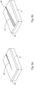
- Figure 6a shows part of the optical coupler during the manufacturing stages, whereby a box layer 49 has been formed on the substrate 41, and the first waveguide element 45 formed on the box layer.
- the first waveguide element 45 may be formed for example in a thin silicon layer on top of the box layer 49, by applying a mask having the desired shape of the first waveguide element 45, and then etching away the unwanted areas of the silicon layer to leave the desired first waveguide element.
- the starting point of the manufacture process may be a SOI wafer comprising the substrate 41, BOX layer 49 and a thin silicon layer on top, from which the first waveguide element 45 is etched. Similar etching techniques can be used to form the second waveguide element 43 over the first waveguide element 45, as shown in Figure 6b , for example by depositing a silicon nitride layer, applying a mask, and etching away to leave the second waveguide element 43.
- one or more areas of sacrificial material or other layers may be deposited during the formation steps, for example to provide a planar surface onto which a subsequent layer may be formed (for example between the stages of forming the first waveguide element and the second waveguide element).
- an optical coupler for example an optical coupler 40 as described in Figures 3a to 3f , or an optical coupler 50 as described in Figures 4a to 4c .
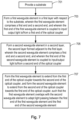
- the method comprises providing a substrate 41, step 701.
- the method comprises forming a first waveguide element 45 in a first layer with respect to the substrate, step 703, wherein the first waveguide element 45 comprises a first end 45a and a second end 45b, and wherein the first end 45a of the first waveguide element 45 is coupled to input/output light to/from a first end of the optical coupler.
- the method comprises forming a second waveguide element 43 in a second layer, the second layer formed adjacent to the first layer, step 705, wherein the second waveguide element 43 comprises a first end 43a and a second end 43b, and wherein the first end 43a of the second waveguide element 43 is coupled to input/output light to/from a second end of the optical coupler.
- the method comprises forming the first waveguide element to extend from the first end of the optical coupler towards the second end of the optical coupler, and forming the second waveguide element 43 to extend from the second end of the optical coupler towards the first end of the optical coupler, such that the first waveguide element 45 overlaps with the second waveguide element 43 to adapt light passing between the first end 45a of the first waveguide element 45 and first end 43a of the second waveguide element 43, step 707.
- the optical coupler is configured to adapt, for example, a mode (such as a spot size) between the first end 45a of the first waveguide element 45 and first end 43a of the second waveguide element 43.
- the starting point of the method is not the formation of a substrate per se, but a SOI wafer that comprises a thin crystalline silicon layer on top (into which the first waveguide element 45 is etched), a BOX (e.g. silicon dioxide) layer underneath and a thick silicon substrate 41 on the bottom.
- SOI wafer that comprises a thin crystalline silicon layer on top (into which the first waveguide element 45 is etched), a BOX (e.g. silicon dioxide) layer underneath and a thick silicon substrate 41 on the bottom.
- the second waveguide element 43 may be formed such that an aspect ratio of the first end 43a of the second waveguide element 43 is less than one, or substantially less than one.
- the second waveguide element 43 may be formed such that a numerical aperture of the first end 43a of the second waveguide element 43 is configured to match the numerical aperture of an external light source coupled thereto.
- the first waveguide element 45 may be formed to taper from having a first width at its first end 45a to having a second width at its second end 45b.
- the second waveguide element may be formed to comprise an expansion region 43 1 and a compression region 43 3 , wherein forming the expansion region 43 1 comprises forming an increasing taper/width from a third width at the first end 43a of the second waveguide element 43 to a larger, fourth width, at an interface with the compression region 43 3 , and wherein forming the compression region 43 3 comprises forming a taper from the fourth width to a smaller, fifth width, at the second end 43b of the second waveguide element.
- the second waveguide element 43 may be formed to comprise an expansion region 43 1 , a constant width region 43 2 , and a compression region 43 3 .
- Forming the expansion region 43 1 comprises forming an increasing taper/width from a third width at the first end 43a of the second waveguide element 43 to a larger, fourth width, at an interface with the constant width section 43 2 , and wherein forming the constant width region 43 2 comprises forming a region having the fourth width between the expansion region 43 1 and the compression region 43 3 , and wherein forming the compression region 43 3 comprises forming a taper from the fourth width to a smaller, fifth width, at the second end 43b of the second waveguide element 43.
- the first waveguide element 45 and second waveguide element 43 of the optical coupler may be formed using first and second masks using complementary metal oxide semiconductor, CMOS, processing techniques.
- a specific design example has been investigated and simulated in order to evaluate the performances of a SSC according to the examples described herein, and in particular the effects of thickness tolerance, alignment tolerance and spacing tolerance.
- the design parameters of the SSC have been optimized by the use of Finite Difference Time Domain (FDTD) simulations.
- FDTD Finite Difference Time Domain
- the simulated coupling loss is about 0.8 dB with ideal horizontal and vertical alignment.
- first and second waveguide elements 45, 43 have different thicknesses, whereas in the drawings the thicknesses appear to be the same. This is because the drawings are not to scale, but provided for illustrative purposes only.
- the first waveguide element 45 and the second waveguide element 43 may be separated, for example by a thin gap, or by a thin layer of material, such as silicon dioxide, SiO 2 .
- a separation of between 0 to 1 ⁇ m, for example 70nm may be provided between a first waveguide element 45, for example a SOI waveguide, and a second waveguide element 43, for example a Si 3 N 4 waveguide, wherein the separation is provided by a layer of material such as SiO 2 .
- a layer may be provided in some technological processes, for example where the etching of the silicon nitride waveguide can damage the silicon waveguide underneath. For this reason, first a very thin layer, e.g.
- a layer ranging from 0 to 1 ⁇ m can be deposited between the first waveguide element 45 and the second waveguide element 43. It is noted that such a layer may be provided in any of the embodiments described herein.
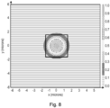
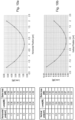
- Figures 9a and 9b illustrate the tolerance to errors in the thickness of the second waveguide element 43.
- Figure 9b shows an end view of the first waveguide element 43 as defined in the list above, i.e. having an ideal thickness of 70nm and a width (the "third" width of Figures 3a to 3c ) of 3 ⁇ m, surrounded by a cladding layer 47.
- the refractive index n a of the silicon nitride waveguide element 43 is shown as being 1.98
- the refractive index n b of the cladding layer 47 is shown as being 1.44.
- Figures 10 and 10b illustrate the tolerance of an optical coupler as described herein to alignment errors.
- Figure 10a shows the tolerance to horizontal position. As can be seen, with a horizontal misalignment of +/- 1 ⁇ m the extra loss is about 1 dB, which is a figure suitable for allowing passive alignment by a typical flip-chip machine.
- Figure 10b shows the tolerance to vertical position.
- the optical coupler is less tolerant to vertical alignment.
- this is not an issue because in the vertical axis it is relatively easy to achieve high accuracy because the SOA is placed in contact with the BOX layer, and that accuracy may also be increased by using pedestals in the BOX layer.
- Figure 11 illustrates the effect of the spacing, during use, of the spacing between the SOA/laser module 61 of Figure 5 and the first waveguide element 43 of the optical coupler 40;50 of Figure 5 (for example simulated without antireflection, A/R, coating at the SOA facet, the A/R coating being an option to help avoid that the light is reflected back at the interface between the two materials).
- the optical coupler is quite tolerant to spacing errors.
- an optical coupler for example a SSC, having a new circuit configuration and a new geometry.
- this new geometry makes use of a silicon nitride material having an index of refraction higher than silica.
- the embodiments described herein have an advantage of being able to provide an optical coupler which, for example, is a few tens of micrometer long, compared to lengths of several hundred micrometers for existing SSC designs.
- the ability to provide a SSC having a small size is particularly advantageous in target applications such as those involving the integration of SOA/laser with a silicon photonic substrate in high integration scale photonic system on chip. In such applications the higher miniaturization results in a higher bandwidth density of the chip.
- the embodiments described herein are much smaller than the SSCs of the prior art without impacting on the performances in terms of coupling loss and alignment tolerance.
- the embodiments therefore enable the density of the photonic integrated circuit in a silicon photonic system on chip to be increased.
- first waveguide element e.g. silicon waveguide
- second waveguide element e.g. silicon nitride waveguide
Landscapes
- Physics & Mathematics (AREA)
- General Physics & Mathematics (AREA)
- Optics & Photonics (AREA)
- Engineering & Computer Science (AREA)
- Microelectronics & Electronic Packaging (AREA)
- Power Engineering (AREA)
- Optical Integrated Circuits (AREA)
Claims (15)
- Coupleur optique comprenant :un substrat (41) ;un premier élément de guide d'ondes (45) disposé dans une première couche par rapport au substrat (41), dans lequel le premier élément de guide d'ondes (45) comprend une première extrémité (45a) et une seconde extrémité (45b), et dans lequel la première extrémité (45a) du premier élément de guide d'ondes (45) est couplé à une lumière d'entrée/sortie vers/depuis une première extrémité du coupleur optique ;dans lequel le premier élément de guide d'ondes (45) diminue en largeur depuis une première largeur à sa première extrémité (45a) jusqu'à une deuxième largeur à sa seconde extrémité (45b) ;un second élément de guide d'ondes (43) disposé dans une deuxième couche, la deuxième couche étant disposée de manière adjacente à la première couche, dans lequel le second élément de guide d'ondes (43) comprend une première extrémité (43a) et une seconde extrémité (43b), et dans lequel la première extrémité (43a) du second élément de guide d'ondes (43) est couplée à une lumière d'entrée/sortie vers/depuis une seconde extrémité du coupleur optique ;dans lequel le premier élément de guide d'ondes (45) est configuré pour s'étendre depuis la première extrémité du coupleur optique vers la seconde extrémité du coupleur optique, et dans lequel le second élément de guide d'ondes (43) est configuré pour s'étendre depuis la seconde extrémité du coupleur optique vers la première extrémité du coupleur optique, de telle sorte que le premier élément de guide d'ondes (45) chevauche le second élément de guide d'ondes (43) pour adapter la lumière passant entre la première extrémité du premier élément de guide d'ondes (45) et la première extrémité (43a) du second élément de guide d'ondes (43),dans lequel le second élément de guide d'ondes (43) comprend :une région d'expansion (431) ; etune région de compression (433) ;
dans lequel la région d'expansion (431) comprend une largeur croissante depuis une troisième largeur au niveau de la première extrémité (43a) du second élément de guide d'ondes (43) jusqu'à une quatrième largeur plus grande, au niveau d'une interface avec la région de compression (433), et dans lequel la région de compression (433) diminue en largeur depuis la quatrième largeur pour avoir une cinquième largeur plus petite, au niveau de la seconde extrémité (43b) du second élément de guide d'ondes (43) ;
caractérisé en ce quele premier élément de guide d'ondes (45) est configuré pour chevaucher le second élément de guide d'ondes (43) de telle sorte que la seconde extrémité (45b) du premier élément de guide d'ondes (45) chevauche au moins partiellement la région d'expansion (431) du second élément de guide d'ondes (43). - Coupleur optique selon la revendication 1, dans lequel le rapport d'aspect de la première extrémité du second élément de guide d'ondes est :inférieur à un ; ousensiblement inférieur à un.
- Coupleur optique selon la revendication 1 ou 2,
dans lequel le premier élément de guide d'ondes (45) comprend une première section ayant une première largeur constante à partir de sa première extrémité (45a), et une seconde section qui se rétrécit à partir de la section de largeur constante jusqu'à une deuxième largeur plus petite au niveau de sa seconde extrémité (45b). - Coupleur optique (40 ; 50) selon les revendications 1 ou 2, dans lequel la largeur du premier élément de guide d'ondes (45) se rétrécit uniformément depuis la première largeur au niveau de sa première extrémité (45a) jusqu'à un point au niveau de sa seconde extrémité (45b).
- Coupleur optique (40) selon l'une quelconque des revendications 1 à 4, dans lequel le second élément de guide d'ondes (43) comprend :la région d'expansion (431) ;une région de largeur constante (432) ; etla région de compression (433) ;
dans lequel la région d'expansion (431) comprend une largeur croissante depuis une troisième largeur au niveau de la première extrémité (43a) du second élément de guide d'ondes (43) jusqu'à une quatrième largeur plus grande, au niveau d'une interface avec la région de largeur constante (432), et dans lequel la région de largeur constante (432) comprend la quatrième largeur entre la région d'expansion (431) et la région de compression (433), et dans lequel la région de compression (433) se rétrécit à partir de la quatrième largeur pour avoir une cinquième largeur plus petite, au niveau de la seconde extrémité (43b) du second élément de guide d'ondes (43). - Coupleur optique (40 ; 50) selon l'une quelconque des revendications précédentes, dans lequel :le premier élément de guide d'ondes (45) comprend une première longueur (LwG1), la première longueur (LwG1I) étant plus courte que la longueur du coupleur optique ; etle second élément de guide d'ondes (43) comprend une seconde longueur (LwG2), la seconde longueur (LwG2) étant plus courte que la longueur du coupleur optique.
- Coupleur optique (40 ; 50) selon la revendication 6, lorsqu'elle dépend de la revendication 1 ou 5, dans lequel le premier élément de guide d'ondes (45) est configuré pour chevaucher le second élément de guide d'ondes (43) de telle sorte que :la seconde extrémité (43b) du second élément de guide d'ondes (43) chevauche une section conique du premier élément de guide d'ondes (45) ; oula seconde extrémité (43b) du second élément de guide d'ondes (43) chevauche une section conique et une partie d'une section de largeur constante du premier élément de guide d'ondes (45).
- Coupleur optique (40 ; 50) selon l'une quelconque des revendications précédentes, dans lequel :le premier élément guide d'ondes (45) comprend une épaisseur constante dans la première couche ; et/oule second élément de guide d'ondes (43) comprend une épaisseur constante dans la deuxième couche ; et/ou,dans lequel la première extrémité (45a) du premier élément de guide d'ondes (45) vient en butée contre le premier côté du coupleur optique, et dans lequel la première extrémité (43a) du second élément de guide d'ondes (43) vient en butée contre le second côté du coupleur optique, de telle sorte que cette lumière peut être couplée entre les première et seconde extrémités du coupleur optique ; et/ou, dans lequel le premier élément de guide d'ondes (45) est formé de silicium, Si ; et/ou comprenant en outre une couche de revêtement (47) entourant le second élément de guide d'ondes (43), et dans lequel le second élément de guide d'ondes (43) est formé à partir d'un matériau ayant un indice de réfraction supérieur à celui de la couche de revêtement (47) ; et/ou, dans lequel le second élément de guide d'ondes (43) est formé de nitrure de silicium, Si3N4.
- Coupleur optique (40 ; 50) selon l'une quelconque des revendications précédentes, dans lequel le coupleur optique comprend un convertisseur de taille de spot, SSC, pour coupler la lumière entre un premier module ayant un signal lumineux comprenant une première forme de mode, et un second module ayant un signal lumineux comprenant une seconde forme de mode, et dans lequel le coupleur optique est configuré pour adapter la lumière entre la première forme de mode et la seconde forme de mode, ou vice versa.
- Coupleur optique (40 ; 50) selon la revendication 9, dans lequel l'indice de réfraction de la couche de gainage (47) est inférieur à l'indice de réfraction du second élément de guide d'ondes (43) et supérieur à l'indice de réfraction d'une troisième couche (49) disposée entre le premier élément de guide d'ondes (45) et le substrat (41) et éventuellement, dans lequel la couche de revêtement (47) comprend du dioxyde de silicium, SiO2, ou dans lequel la couche de revêtement (47) comprend du dioxyde de silicium non stœchiométrique, SiOx, et/ou dans lequel la troisième couche comprend une couche d'oxyde enterrée, BOX, (49) .
- Dispositif photonique à semi-conducteur (60) comprenant :un premier module optique ;un second module optique ; etun coupleur optique tel que défini dans l'une quelconque des revendications 1 à 10, pour coupler la lumière entre le premier module optique et le second module optique.
- Procédé de formation d'un coupleur optique (40 ; 50), le procédé comprenant :la fourniture d'un substrat (étape 701) ;la formation (étape 703) d'un premier élément de guide d'ondes (45) dans une première couche par rapport au substrat, dans lequel le premier élément de guide d'ondes (45) comprend une première extrémité (45a) et une seconde extrémité (45b), et dans lequel la première extrémité (45a) du premier élément de guide d'ondes (45) est couplée à une lumière d'entrée/sortie vers/depuis une première extrémité du coupleur optique ;dans lequel le premier élément de guide d'ondes (45) diminue en largeur, passant d'une première largeur à sa première extrémité (45a) à une deuxième largeur à sa seconde extrémité (45b).la formation (étape 705) d'un second élément de guide d'ondes (43) dans une deuxième couche, la deuxième couche étant formée de manière adjacente à la première couche, dans lequel le second élément de guide d'ondes (43) comprend une première extrémité (43a) et une seconde extrémité (43b), et dans lequel la première extrémité (43a) du second élément de guide d'ondes (43) est couplée à une lumière d'entrée/sortie vers/depuis une seconde extrémité du coupleur optique ;dans lequel le premier élément de guide d'ondes (45) est formé pour s'étendre depuis la première extrémité du coupleur optique vers la seconde extrémité du coupleur optique, et dans lequel le second élément de guide d'ondes (43) est formé pour s'étendre depuis la seconde extrémité du coupleur optique vers la première extrémité du coupleur optique, de telle sorte que le premier élément de guide d'ondes (45) chevauche le second élément de guide d'ondes (43) pour adapter la lumière passant entre la première extrémité (45a) du premier élément de guide d'ondes et la première extrémité (43a) du second élément de guide d'ondes (43) comprenant la formation du second élément de guide d'ondes pour qu'il comprenne :une région d'expansion ; etune région de compression ;dans lequel la formation de la région d'expansion comprend la formation d'une largeur croissante depuis une troisième largeur au niveau de la première extrémité du second élément de guide d'ondes jusqu'à une quatrième largeur plus grande, au niveau d'une interface avec la région de compression, etdans lequel la formation de la région de compression comprend la formation d'une largeur diminuant depuis la quatrième largeur jusqu'à une cinquième largeur plus petite, au niveau de la seconde extrémité du second élément de guide d'ondes ; etdans lequel le premier élément de guide d'ondes est configuré pour chevaucher le second élément de guide d'ondes de telle sorte que la seconde extrémité du premier élément de guide d'ondes chevauche au moins partiellement la région d'expansion du second élément de guide d'ondes.
- Procédé selon la revendication 12, dans lequel le second élément de guide d'ondes (43) est formé de telle sorte qu'un rapport d'aspect de la première extrémité (43a) du second élément de guide d'ondes (43) soit :inférieur à un ; ousensiblement inférieur à un.
- Procédé selon la revendication 12 ou 13, dans lequel le second élément de guide d'ondes (43) est formé de telle sorte qu'une ouverture numérique de la première extrémité (43a) du second élément de guide d'ondes (43) est configurée pour correspondre à l'ouverture numérique d'un appareil externe d'une source de lumière qui y est couplée ; et/ou,
la formation du premier élément de guide d'ondes (45) pour qu'il comprenne une première section ayant une première largeur constante à partir de sa première extrémité (45a), et une seconde section dont la largeur diminue à partir de la section de largeur constante jusqu'à une deuxième largeur plus petite au niveau de sa seconde extrémité (45b). - Procédé selon l'une quelconque des revendications 12 à 14, dans lequel la formation du second élément de guide d'ondes (43) comprend :la région d'expansion (431) ;une région de largeur constante (432) ; etla région de compression (433) ;dans lequel la formation de la région d'expansion (431) comprend la formation d'une largeur croissante depuis une troisième largeur au niveau de la première extrémité (43a) du second élément de guide d'ondes (43) jusqu'à une quatrième largeur plus grande, au niveau d'une interface avec la région de largeur constante (432) ; etdans lequel la formation de la région de largeur constante (432) comprend la formation d'une région ayant la quatrième largeur entre la région d'expansion (431) et la région de compression (433) ; etdans lequel la formation de la région de compression (433) comprend la formation d'une largeur diminuant depuis la quatrième largeur jusqu'à une cinquième largeur plus petite, au niveau de la seconde extrémité (43b) du second élément de guide d'ondes (43) ; et/ou, dans lequel le premier élément de guide d'ondes est formé de silicium, Si, et/ou dans lequel le second élément de guide d'ondes est formé de nitrure de silicium, Si3N4 ; et/ou dans lequel le premier élément de guide d'ondes et le second élément de guide d'ondes du coupleur optique sont formés à l'aide de premier et de second masques utilisant des techniques de traitement complémentaires à semiconducteur à oxyde métallique, CMOS.
Applications Claiming Priority (1)
| Application Number | Priority Date | Filing Date | Title |
|---|---|---|---|
| PCT/EP2017/050580 WO2018130285A1 (fr) | 2017-01-12 | 2017-01-12 | Appareil et procédé de couplage de lumière |
Publications (3)
| Publication Number | Publication Date |
|---|---|
| EP3568721A1 EP3568721A1 (fr) | 2019-11-20 |
| EP3568721C0 EP3568721C0 (fr) | 2024-05-29 |
| EP3568721B1 true EP3568721B1 (fr) | 2024-05-29 |
Family
ID=57868229
Family Applications (1)
| Application Number | Title | Priority Date | Filing Date |
|---|---|---|---|
| EP17701070.9A Active EP3568721B1 (fr) | 2017-01-12 | 2017-01-12 | Appareil et procédé de couplage de lumière |
Country Status (3)
| Country | Link |
|---|---|
| US (1) | US10852484B2 (fr) |
| EP (1) | EP3568721B1 (fr) |
| WO (1) | WO2018130285A1 (fr) |
Families Citing this family (17)
| Publication number | Priority date | Publication date | Assignee | Title |
|---|---|---|---|---|
| WO2018119226A1 (fr) * | 2016-12-21 | 2018-06-28 | Acacia Communications, Inc. | Multiplexeur à division de longueur d'onde |
| US11031381B2 (en) * | 2018-10-30 | 2021-06-08 | Taiwan Semiconductor Manufacturing Company, Ltd. | Optical transceiver and manufacturing method thereof |
| US10534136B1 (en) | 2018-12-18 | 2020-01-14 | Honeywell International Inc. | High-efficiency fiber-to-waveguide coupler |
| CN109597162B (zh) * | 2018-12-27 | 2021-04-09 | 华为技术有限公司 | 平面光波导、plc芯片、光束整形结构及wss |
| FR3098312B1 (fr) * | 2019-07-05 | 2023-01-06 | Almae Tech | composant semi-conducteur actif, composant passif à base de silicium, assemblage desdits composants et procédé de couplage entre guides d’ondes |
| CN113359234B (zh) * | 2020-03-02 | 2023-05-16 | 苏州旭创科技有限公司 | 一种模斑变换器及硅光集成芯片 |
| US11550200B2 (en) * | 2020-03-04 | 2023-01-10 | Globalfoundries U.S. Inc. | Reconfigurable optical grating/coupler |
| US11204469B1 (en) | 2020-06-01 | 2021-12-21 | Honeywell International Inc. | Apparatus for high-efficiency fiber-to-chip coupling and mode-conversion to integrated photonics platform |
| US11609379B2 (en) * | 2020-10-21 | 2023-03-21 | Globalfoundries U.S. Inc. | Structures for managing light polarization states on a photonics chip |
| CA3158693A1 (fr) * | 2021-05-14 | 2022-11-14 | Ranovus Inc. | Coupleur en guide d'ondes |
| CN115808736B (zh) * | 2021-09-15 | 2026-01-27 | 华为技术有限公司 | 光耦合器、光芯片和光通信设备 |
| US12066671B2 (en) * | 2022-01-12 | 2024-08-20 | Taiwan Semiconductor Manufacturing Company, Ltd. | Semiconductor devices with vertically stacked and laterally offset intermediate waveguides |
| JP2024061994A (ja) * | 2022-10-24 | 2024-05-09 | 富士通オプティカルコンポーネンツ株式会社 | 光デバイス、光送信器及び光受信器 |
| US12625319B2 (en) * | 2022-11-02 | 2026-05-12 | Openlight Photonics, Inc. | Waveguide transitions for hybrid thin-silicon/III-V photonics |
| JP2024068967A (ja) | 2022-11-09 | 2024-05-21 | 富士通株式会社 | アレイアンテナシステム、非線形歪み抑制方法、及び無線装置 |
| US20250125587A1 (en) * | 2023-10-13 | 2025-04-17 | Openlight Photonics, Inc. | Laser with edge coupler displaced from substrate |
| CN118377085B (zh) * | 2024-06-24 | 2024-09-17 | 杭州质禾科技有限公司 | 一种光芯片结构 |
Citations (1)
| Publication number | Priority date | Publication date | Assignee | Title |
|---|---|---|---|---|
| US20110116741A1 (en) * | 2008-02-29 | 2011-05-19 | Gaia Cevini | Optical mode transformer, in particular for coupling an optical fiber and a high-index contrast waveguide |
Family Cites Families (9)
| Publication number | Priority date | Publication date | Assignee | Title |
|---|---|---|---|---|
| JP3941334B2 (ja) | 2000-04-20 | 2007-07-04 | 株式会社日立製作所 | 光伝送モジュールおよびそれを用いた光通信システム |
| US8031991B2 (en) | 2008-05-28 | 2011-10-04 | Lightwire Inc. | Low index, large mode field diameter optical coupler |
| US8761552B1 (en) | 2009-12-08 | 2014-06-24 | University Of Washington Through Its Center For Commercialization | Fabricating waveguides in conjunction with interconnect fabrication in back-ends of integrated circuits and structures thereof |
| US8264919B2 (en) * | 2010-02-25 | 2012-09-11 | Tdk Corporation | Thermal assisted magnetic recording head having spot size converter |
| JP5764776B2 (ja) * | 2010-10-08 | 2015-08-19 | 国立研究開発法人産業技術総合研究所 | 光学変換素子 |
| US20130236193A1 (en) | 2012-03-09 | 2013-09-12 | Commscope, Inc. Of North Carolina | Optical Communications Systems that Couple Optical Signals from a Large Core Fiber to a Smaller Core Fiber and Related Methods and Apparatus |
| CN106461873B (zh) * | 2014-04-30 | 2021-04-20 | 华为技术有限公司 | 低损耗模转换器及其制作方法 |
| IT201700047081A1 (it) * | 2017-05-02 | 2018-11-02 | St Microelectronics Srl | Guida d'onda ottica, dispositivo di accoppiamento e procedimento corrispondenti |
| US10429582B1 (en) * | 2018-05-02 | 2019-10-01 | Globalfoundries Inc. | Waveguide-to-waveguide couplers with multiple tapers |
-
2017
- 2017-01-12 US US16/477,758 patent/US10852484B2/en active Active
- 2017-01-12 WO PCT/EP2017/050580 patent/WO2018130285A1/fr not_active Ceased
- 2017-01-12 EP EP17701070.9A patent/EP3568721B1/fr active Active
Patent Citations (1)
| Publication number | Priority date | Publication date | Assignee | Title |
|---|---|---|---|---|
| US20110116741A1 (en) * | 2008-02-29 | 2011-05-19 | Gaia Cevini | Optical mode transformer, in particular for coupling an optical fiber and a high-index contrast waveguide |
Also Published As
| Publication number | Publication date |
|---|---|
| EP3568721C0 (fr) | 2024-05-29 |
| US20190369333A1 (en) | 2019-12-05 |
| WO2018130285A1 (fr) | 2018-07-19 |
| EP3568721A1 (fr) | 2019-11-20 |
| US10852484B2 (en) | 2020-12-01 |
Similar Documents
| Publication | Publication Date | Title |
|---|---|---|
| US10852484B2 (en) | Apparatus and method for coupling light | |
| US8000565B2 (en) | Buried dual taper waveguide for passive alignment and photonic integration | |
| US10698164B2 (en) | Optical apparatus and methods of manufacture thereof | |
| KR101591847B1 (ko) | 효율적인 실리콘-온-인슐레이터 격자 결합기 | |
| US7738753B2 (en) | CMOS compatible integrated dielectric optical waveguide coupler and fabrication | |
| US20130114924A1 (en) | Optical Arrangement and a Method of Forming the Same | |
| US12411286B2 (en) | Edge coupler and manufacturing method therefor | |
| US10096971B2 (en) | Hybrid semiconductor lasers | |
| US10416381B1 (en) | Spot-size-converter design for facet optical coupling | |
| EP3494424B1 (fr) | Convertisseur de taille de tache de faisceau optique | |
| US20150277036A1 (en) | Apparatus and Method for an Optical Waveguide Edge Coupler for Photonic Integrated Chips | |
| TWI867448B (zh) | 具有連續配置之錐形物的邊緣耦合件 | |
| CN113534337B (zh) | 一种硅光子芯片光耦合结构加工方法及结构 | |
| CN114114535A (zh) | 多层硅光子装置 | |
| US11906781B2 (en) | End-face coupling structures underneath a photonic layer | |
| US20240142700A1 (en) | Waveguide transitions for hybrid thin-silicon/iii-v photonics | |
| Snyder et al. | Broadband, polarization-insensitive lensed edge couplers for silicon photonics | |
| CN115793138B (zh) | 光集成器件、光集成电路晶圆以及制造光集成器件的方法 | |
| CN114895401B (zh) | 一种硅光子芯片光耦合结构及其制造方法 | |
| US11808996B1 (en) | Waveguides and edge couplers with multiple-thickness waveguide cores | |
| WO2022044101A1 (fr) | Composant de guide d'ondes optique et son procédé de fabrication | |
| JP2820202B2 (ja) | スポットサイズ変換器の製造方法 | |
| JP2015045789A (ja) | スポットサイズ変換器 | |
| JP2019197126A (ja) | 光デバイスおよび光結合方法 | |
| CN117148493A (zh) | 光芯片及其制造方法 |
Legal Events
| Date | Code | Title | Description |
|---|---|---|---|
| STAA | Information on the status of an ep patent application or granted ep patent |
Free format text: STATUS: UNKNOWN |
|
| STAA | Information on the status of an ep patent application or granted ep patent |
Free format text: STATUS: THE INTERNATIONAL PUBLICATION HAS BEEN MADE |
|
| PUAI | Public reference made under article 153(3) epc to a published international application that has entered the european phase |
Free format text: ORIGINAL CODE: 0009012 |
|
| STAA | Information on the status of an ep patent application or granted ep patent |
Free format text: STATUS: REQUEST FOR EXAMINATION WAS MADE |
|
| 17P | Request for examination filed |
Effective date: 20190712 |
|
| AK | Designated contracting states |
Kind code of ref document: A1 Designated state(s): AL AT BE BG CH CY CZ DE DK EE ES FI FR GB GR HR HU IE IS IT LI LT LU LV MC MK MT NL NO PL PT RO RS SE SI SK SM TR |
|
| AX | Request for extension of the european patent |
Extension state: BA ME |
|
| DAV | Request for validation of the european patent (deleted) | ||
| DAX | Request for extension of the european patent (deleted) | ||
| STAA | Information on the status of an ep patent application or granted ep patent |
Free format text: STATUS: EXAMINATION IS IN PROGRESS |
|
| 17Q | First examination report despatched |
Effective date: 20211112 |
|
| GRAP | Despatch of communication of intention to grant a patent |
Free format text: ORIGINAL CODE: EPIDOSNIGR1 |
|
| STAA | Information on the status of an ep patent application or granted ep patent |
Free format text: STATUS: GRANT OF PATENT IS INTENDED |
|
| INTG | Intention to grant announced |
Effective date: 20240220 |
|
| GRAS | Grant fee paid |
Free format text: ORIGINAL CODE: EPIDOSNIGR3 |
|
| GRAA | (expected) grant |
Free format text: ORIGINAL CODE: 0009210 |
|
| STAA | Information on the status of an ep patent application or granted ep patent |
Free format text: STATUS: THE PATENT HAS BEEN GRANTED |
|
| AK | Designated contracting states |
Kind code of ref document: B1 Designated state(s): AL AT BE BG CH CY CZ DE DK EE ES FI FR GB GR HR HU IE IS IT LI LT LU LV MC MK MT NL NO PL PT RO RS SE SI SK SM TR |
|
| REG | Reference to a national code |
Ref country code: CH Ref legal event code: EP |
|
| REG | Reference to a national code |
Ref country code: IE Ref legal event code: FG4D |
|
| REG | Reference to a national code |
Ref country code: DE Ref legal event code: R096 Ref document number: 602017082253 Country of ref document: DE |
|
| U01 | Request for unitary effect filed |
Effective date: 20240606 |
|
| U07 | Unitary effect registered |
Designated state(s): AT BE BG DE DK EE FI FR IT LT LU LV MT NL PT SE SI Effective date: 20240620 |
|
| PG25 | Lapsed in a contracting state [announced via postgrant information from national office to epo] |
Ref country code: IS Free format text: LAPSE BECAUSE OF FAILURE TO SUBMIT A TRANSLATION OF THE DESCRIPTION OR TO PAY THE FEE WITHIN THE PRESCRIBED TIME-LIMIT Effective date: 20240929 |
|
| PG25 | Lapsed in a contracting state [announced via postgrant information from national office to epo] |
Ref country code: HR Free format text: LAPSE BECAUSE OF FAILURE TO SUBMIT A TRANSLATION OF THE DESCRIPTION OR TO PAY THE FEE WITHIN THE PRESCRIBED TIME-LIMIT Effective date: 20240529 |
|
| PG25 | Lapsed in a contracting state [announced via postgrant information from national office to epo] |
Ref country code: GR Free format text: LAPSE BECAUSE OF FAILURE TO SUBMIT A TRANSLATION OF THE DESCRIPTION OR TO PAY THE FEE WITHIN THE PRESCRIBED TIME-LIMIT Effective date: 20240830 |
|
| PG25 | Lapsed in a contracting state [announced via postgrant information from national office to epo] |
Ref country code: ES Free format text: LAPSE BECAUSE OF FAILURE TO SUBMIT A TRANSLATION OF THE DESCRIPTION OR TO PAY THE FEE WITHIN THE PRESCRIBED TIME-LIMIT Effective date: 20240529 |
|
| PG25 | Lapsed in a contracting state [announced via postgrant information from national office to epo] |
Ref country code: PL Free format text: LAPSE BECAUSE OF FAILURE TO SUBMIT A TRANSLATION OF THE DESCRIPTION OR TO PAY THE FEE WITHIN THE PRESCRIBED TIME-LIMIT Effective date: 20240529 |
|
| PG25 | Lapsed in a contracting state [announced via postgrant information from national office to epo] |
Ref country code: PL Free format text: LAPSE BECAUSE OF FAILURE TO SUBMIT A TRANSLATION OF THE DESCRIPTION OR TO PAY THE FEE WITHIN THE PRESCRIBED TIME-LIMIT Effective date: 20240529 Ref country code: NO Free format text: LAPSE BECAUSE OF FAILURE TO SUBMIT A TRANSLATION OF THE DESCRIPTION OR TO PAY THE FEE WITHIN THE PRESCRIBED TIME-LIMIT Effective date: 20240829 Ref country code: IS Free format text: LAPSE BECAUSE OF FAILURE TO SUBMIT A TRANSLATION OF THE DESCRIPTION OR TO PAY THE FEE WITHIN THE PRESCRIBED TIME-LIMIT Effective date: 20240929 Ref country code: HR Free format text: LAPSE BECAUSE OF FAILURE TO SUBMIT A TRANSLATION OF THE DESCRIPTION OR TO PAY THE FEE WITHIN THE PRESCRIBED TIME-LIMIT Effective date: 20240529 Ref country code: GR Free format text: LAPSE BECAUSE OF FAILURE TO SUBMIT A TRANSLATION OF THE DESCRIPTION OR TO PAY THE FEE WITHIN THE PRESCRIBED TIME-LIMIT Effective date: 20240830 Ref country code: ES Free format text: LAPSE BECAUSE OF FAILURE TO SUBMIT A TRANSLATION OF THE DESCRIPTION OR TO PAY THE FEE WITHIN THE PRESCRIBED TIME-LIMIT Effective date: 20240529 Ref country code: RS Free format text: LAPSE BECAUSE OF FAILURE TO SUBMIT A TRANSLATION OF THE DESCRIPTION OR TO PAY THE FEE WITHIN THE PRESCRIBED TIME-LIMIT Effective date: 20240829 |
|
| PG25 | Lapsed in a contracting state [announced via postgrant information from national office to epo] |
Ref country code: CZ Free format text: LAPSE BECAUSE OF FAILURE TO SUBMIT A TRANSLATION OF THE DESCRIPTION OR TO PAY THE FEE WITHIN THE PRESCRIBED TIME-LIMIT Effective date: 20240529 |
|
| PG25 | Lapsed in a contracting state [announced via postgrant information from national office to epo] |
Ref country code: SK Free format text: LAPSE BECAUSE OF FAILURE TO SUBMIT A TRANSLATION OF THE DESCRIPTION OR TO PAY THE FEE WITHIN THE PRESCRIBED TIME-LIMIT Effective date: 20240529 Ref country code: RO Free format text: LAPSE BECAUSE OF FAILURE TO SUBMIT A TRANSLATION OF THE DESCRIPTION OR TO PAY THE FEE WITHIN THE PRESCRIBED TIME-LIMIT Effective date: 20240529 |
|
| PG25 | Lapsed in a contracting state [announced via postgrant information from national office to epo] |
Ref country code: SM Free format text: LAPSE BECAUSE OF FAILURE TO SUBMIT A TRANSLATION OF THE DESCRIPTION OR TO PAY THE FEE WITHIN THE PRESCRIBED TIME-LIMIT Effective date: 20240529 |
|
| PG25 | Lapsed in a contracting state [announced via postgrant information from national office to epo] |
Ref country code: SM Free format text: LAPSE BECAUSE OF FAILURE TO SUBMIT A TRANSLATION OF THE DESCRIPTION OR TO PAY THE FEE WITHIN THE PRESCRIBED TIME-LIMIT Effective date: 20240529 Ref country code: SK Free format text: LAPSE BECAUSE OF FAILURE TO SUBMIT A TRANSLATION OF THE DESCRIPTION OR TO PAY THE FEE WITHIN THE PRESCRIBED TIME-LIMIT Effective date: 20240529 Ref country code: RO Free format text: LAPSE BECAUSE OF FAILURE TO SUBMIT A TRANSLATION OF THE DESCRIPTION OR TO PAY THE FEE WITHIN THE PRESCRIBED TIME-LIMIT Effective date: 20240529 Ref country code: CZ Free format text: LAPSE BECAUSE OF FAILURE TO SUBMIT A TRANSLATION OF THE DESCRIPTION OR TO PAY THE FEE WITHIN THE PRESCRIBED TIME-LIMIT Effective date: 20240529 |
|
| U20 | Renewal fee for the european patent with unitary effect paid |
Year of fee payment: 9 Effective date: 20250127 |
|
| PLBE | No opposition filed within time limit |
Free format text: ORIGINAL CODE: 0009261 |
|
| STAA | Information on the status of an ep patent application or granted ep patent |
Free format text: STATUS: NO OPPOSITION FILED WITHIN TIME LIMIT |
|
| 26N | No opposition filed |
Effective date: 20250303 |
|
| REG | Reference to a national code |
Ref country code: CH Ref legal event code: PL |
|
| PG25 | Lapsed in a contracting state [announced via postgrant information from national office to epo] |
Ref country code: MC Free format text: LAPSE BECAUSE OF FAILURE TO SUBMIT A TRANSLATION OF THE DESCRIPTION OR TO PAY THE FEE WITHIN THE PRESCRIBED TIME-LIMIT Effective date: 20240529 |
|
| GBPC | Gb: european patent ceased through non-payment of renewal fee |
Effective date: 20250112 |
|
| PG25 | Lapsed in a contracting state [announced via postgrant information from national office to epo] |
Ref country code: GB Free format text: LAPSE BECAUSE OF NON-PAYMENT OF DUE FEES Effective date: 20250112 |
|
| PG25 | Lapsed in a contracting state [announced via postgrant information from national office to epo] |
Ref country code: CH Free format text: LAPSE BECAUSE OF NON-PAYMENT OF DUE FEES Effective date: 20250131 |
|
| PG25 | Lapsed in a contracting state [announced via postgrant information from national office to epo] |
Ref country code: IE Free format text: LAPSE BECAUSE OF NON-PAYMENT OF DUE FEES Effective date: 20250112 |
|
| U20 | Renewal fee for the european patent with unitary effect paid |
Year of fee payment: 10 Effective date: 20260127 |
|
| PG25 | Lapsed in a contracting state [announced via postgrant information from national office to epo] |
Ref country code: CY Free format text: LAPSE BECAUSE OF FAILURE TO SUBMIT A TRANSLATION OF THE DESCRIPTION OR TO PAY THE FEE WITHIN THE PRESCRIBED TIME-LIMIT Effective date: 20240529 |
|
| PG25 | Lapsed in a contracting state [announced via postgrant information from national office to epo] |
Ref country code: TR Free format text: LAPSE BECAUSE OF FAILURE TO SUBMIT A TRANSLATION OF THE DESCRIPTION OR TO PAY THE FEE WITHIN THE PRESCRIBED TIME-LIMIT Effective date: 20240529 |