EP3568727B1 - Rückbeleuchtung und herstellungsverfahren dafür, lichtleiterplatte und herstellungsverfahren dafür und anzeigevorrichtung - Google Patents
Rückbeleuchtung und herstellungsverfahren dafür, lichtleiterplatte und herstellungsverfahren dafür und anzeigevorrichtung Download PDFInfo
- Publication number
- EP3568727B1 EP3568727B1 EP17842314.1A EP17842314A EP3568727B1 EP 3568727 B1 EP3568727 B1 EP 3568727B1 EP 17842314 A EP17842314 A EP 17842314A EP 3568727 B1 EP3568727 B1 EP 3568727B1
- Authority
- EP
- European Patent Office
- Prior art keywords
- guide plate
- light guide
- light
- light emitting
- main body
- Prior art date
- Legal status (The legal status is an assumption and is not a legal conclusion. Google has not performed a legal analysis and makes no representation as to the accuracy of the status listed.)
- Active
Links
Images


Classifications
-
- G—PHYSICS
- G02—OPTICS
- G02F—OPTICAL DEVICES OR ARRANGEMENTS FOR THE CONTROL OF LIGHT BY MODIFICATION OF THE OPTICAL PROPERTIES OF THE MEDIA OF THE ELEMENTS INVOLVED THEREIN; NON-LINEAR OPTICS; FREQUENCY-CHANGING OF LIGHT; OPTICAL LOGIC ELEMENTS; OPTICAL ANALOGUE/DIGITAL CONVERTERS
- G02F1/00—Devices or arrangements for the control of the intensity, colour, phase, polarisation or direction of light arriving from an independent light source, e.g. switching, gating or modulating; Non-linear optics
- G02F1/01—Devices or arrangements for the control of the intensity, colour, phase, polarisation or direction of light arriving from an independent light source, e.g. switching, gating or modulating; Non-linear optics for the control of the intensity, phase, polarisation or colour
- G02F1/13—Devices or arrangements for the control of the intensity, colour, phase, polarisation or direction of light arriving from an independent light source, e.g. switching, gating or modulating; Non-linear optics for the control of the intensity, phase, polarisation or colour based on liquid crystals, e.g. single liquid crystal display cells
- G02F1/133—Constructional arrangements; Operation of liquid crystal cells; Circuit arrangements
- G02F1/1333—Constructional arrangements; Manufacturing methods
- G02F1/1335—Structural association of cells with optical devices, e.g. polarisers or reflectors
- G02F1/1336—Illuminating devices
- G02F1/133602—Direct backlight
- G02F1/133603—Direct backlight with LEDs
-
- G—PHYSICS
- G02—OPTICS
- G02B—OPTICAL ELEMENTS, SYSTEMS OR APPARATUS
- G02B6/00—Light guides; Structural details of arrangements comprising light guides and other optical elements, e.g. couplings
- G02B6/0001—Light guides; Structural details of arrangements comprising light guides and other optical elements, e.g. couplings specially adapted for lighting devices or systems
- G02B6/0011—Light guides; Structural details of arrangements comprising light guides and other optical elements, e.g. couplings specially adapted for lighting devices or systems the light guides being planar or of plate-like form
- G02B6/0013—Means for improving the coupling-in of light from the light source into the light guide
- G02B6/0023—Means for improving the coupling-in of light from the light source into the light guide provided by one optical element, or plurality thereof, placed between the light guide and the light source, or around the light source
- G02B6/0031—Reflecting element, sheet or layer
-
- G—PHYSICS
- G02—OPTICS
- G02B—OPTICAL ELEMENTS, SYSTEMS OR APPARATUS
- G02B6/00—Light guides; Structural details of arrangements comprising light guides and other optical elements, e.g. couplings
- G02B6/0001—Light guides; Structural details of arrangements comprising light guides and other optical elements, e.g. couplings specially adapted for lighting devices or systems
- G02B6/0011—Light guides; Structural details of arrangements comprising light guides and other optical elements, e.g. couplings specially adapted for lighting devices or systems the light guides being planar or of plate-like form
- G02B6/0033—Means for improving the coupling-out of light from the light guide
- G02B6/0035—Means for improving the coupling-out of light from the light guide provided on the surface of the light guide or in the bulk of it
- G02B6/004—Scattering dots or dot-like elements, e.g. microbeads, scattering particles, nanoparticles
-
- G—PHYSICS
- G02—OPTICS
- G02F—OPTICAL DEVICES OR ARRANGEMENTS FOR THE CONTROL OF LIGHT BY MODIFICATION OF THE OPTICAL PROPERTIES OF THE MEDIA OF THE ELEMENTS INVOLVED THEREIN; NON-LINEAR OPTICS; FREQUENCY-CHANGING OF LIGHT; OPTICAL LOGIC ELEMENTS; OPTICAL ANALOGUE/DIGITAL CONVERTERS
- G02F1/00—Devices or arrangements for the control of the intensity, colour, phase, polarisation or direction of light arriving from an independent light source, e.g. switching, gating or modulating; Non-linear optics
- G02F1/01—Devices or arrangements for the control of the intensity, colour, phase, polarisation or direction of light arriving from an independent light source, e.g. switching, gating or modulating; Non-linear optics for the control of the intensity, phase, polarisation or colour
- G02F1/13—Devices or arrangements for the control of the intensity, colour, phase, polarisation or direction of light arriving from an independent light source, e.g. switching, gating or modulating; Non-linear optics for the control of the intensity, phase, polarisation or colour based on liquid crystals, e.g. single liquid crystal display cells
- G02F1/133—Constructional arrangements; Operation of liquid crystal cells; Circuit arrangements
- G02F1/1333—Constructional arrangements; Manufacturing methods
- G02F1/1335—Structural association of cells with optical devices, e.g. polarisers or reflectors
- G02F1/1336—Illuminating devices
- G02F1/133602—Direct backlight
- G02F1/133605—Direct backlight including specially adapted reflectors
-
- G—PHYSICS
- G02—OPTICS
- G02F—OPTICAL DEVICES OR ARRANGEMENTS FOR THE CONTROL OF LIGHT BY MODIFICATION OF THE OPTICAL PROPERTIES OF THE MEDIA OF THE ELEMENTS INVOLVED THEREIN; NON-LINEAR OPTICS; FREQUENCY-CHANGING OF LIGHT; OPTICAL LOGIC ELEMENTS; OPTICAL ANALOGUE/DIGITAL CONVERTERS
- G02F1/00—Devices or arrangements for the control of the intensity, colour, phase, polarisation or direction of light arriving from an independent light source, e.g. switching, gating or modulating; Non-linear optics
- G02F1/01—Devices or arrangements for the control of the intensity, colour, phase, polarisation or direction of light arriving from an independent light source, e.g. switching, gating or modulating; Non-linear optics for the control of the intensity, phase, polarisation or colour
- G02F1/13—Devices or arrangements for the control of the intensity, colour, phase, polarisation or direction of light arriving from an independent light source, e.g. switching, gating or modulating; Non-linear optics for the control of the intensity, phase, polarisation or colour based on liquid crystals, e.g. single liquid crystal display cells
- G02F1/133—Constructional arrangements; Operation of liquid crystal cells; Circuit arrangements
- G02F1/1333—Constructional arrangements; Manufacturing methods
- G02F1/1335—Structural association of cells with optical devices, e.g. polarisers or reflectors
- G02F1/1336—Illuminating devices
- G02F1/133602—Direct backlight
- G02F1/133606—Direct backlight including a specially adapted diffusing, scattering or light controlling members
-
- G—PHYSICS
- G02—OPTICS
- G02F—OPTICAL DEVICES OR ARRANGEMENTS FOR THE CONTROL OF LIGHT BY MODIFICATION OF THE OPTICAL PROPERTIES OF THE MEDIA OF THE ELEMENTS INVOLVED THEREIN; NON-LINEAR OPTICS; FREQUENCY-CHANGING OF LIGHT; OPTICAL LOGIC ELEMENTS; OPTICAL ANALOGUE/DIGITAL CONVERTERS
- G02F1/00—Devices or arrangements for the control of the intensity, colour, phase, polarisation or direction of light arriving from an independent light source, e.g. switching, gating or modulating; Non-linear optics
- G02F1/01—Devices or arrangements for the control of the intensity, colour, phase, polarisation or direction of light arriving from an independent light source, e.g. switching, gating or modulating; Non-linear optics for the control of the intensity, phase, polarisation or colour
- G02F1/13—Devices or arrangements for the control of the intensity, colour, phase, polarisation or direction of light arriving from an independent light source, e.g. switching, gating or modulating; Non-linear optics for the control of the intensity, phase, polarisation or colour based on liquid crystals, e.g. single liquid crystal display cells
- G02F1/133—Constructional arrangements; Operation of liquid crystal cells; Circuit arrangements
- G02F1/1333—Constructional arrangements; Manufacturing methods
- G02F1/1335—Structural association of cells with optical devices, e.g. polarisers or reflectors
- G02F1/1336—Illuminating devices
- G02F1/133621—Illuminating devices providing coloured light
-
- G—PHYSICS
- G02—OPTICS
- G02B—OPTICAL ELEMENTS, SYSTEMS OR APPARATUS
- G02B6/00—Light guides; Structural details of arrangements comprising light guides and other optical elements, e.g. couplings
- G02B6/0001—Light guides; Structural details of arrangements comprising light guides and other optical elements, e.g. couplings specially adapted for lighting devices or systems
- G02B6/0011—Light guides; Structural details of arrangements comprising light guides and other optical elements, e.g. couplings specially adapted for lighting devices or systems the light guides being planar or of plate-like form
- G02B6/0013—Means for improving the coupling-in of light from the light source into the light guide
- G02B6/0023—Means for improving the coupling-in of light from the light source into the light guide provided by one optical element, or plurality thereof, placed between the light guide and the light source, or around the light source
- G02B6/0026—Wavelength selective element, sheet or layer, e.g. filter or grating
-
- G—PHYSICS
- G02—OPTICS
- G02F—OPTICAL DEVICES OR ARRANGEMENTS FOR THE CONTROL OF LIGHT BY MODIFICATION OF THE OPTICAL PROPERTIES OF THE MEDIA OF THE ELEMENTS INVOLVED THEREIN; NON-LINEAR OPTICS; FREQUENCY-CHANGING OF LIGHT; OPTICAL LOGIC ELEMENTS; OPTICAL ANALOGUE/DIGITAL CONVERTERS
- G02F1/00—Devices or arrangements for the control of the intensity, colour, phase, polarisation or direction of light arriving from an independent light source, e.g. switching, gating or modulating; Non-linear optics
- G02F1/01—Devices or arrangements for the control of the intensity, colour, phase, polarisation or direction of light arriving from an independent light source, e.g. switching, gating or modulating; Non-linear optics for the control of the intensity, phase, polarisation or colour
- G02F1/13—Devices or arrangements for the control of the intensity, colour, phase, polarisation or direction of light arriving from an independent light source, e.g. switching, gating or modulating; Non-linear optics for the control of the intensity, phase, polarisation or colour based on liquid crystals, e.g. single liquid crystal display cells
- G02F1/133—Constructional arrangements; Operation of liquid crystal cells; Circuit arrangements
- G02F1/1333—Constructional arrangements; Manufacturing methods
- G02F1/1335—Structural association of cells with optical devices, e.g. polarisers or reflectors
- G02F1/1336—Illuminating devices
- G02F1/133602—Direct backlight
- G02F1/133606—Direct backlight including a specially adapted diffusing, scattering or light controlling members
- G02F1/133607—Direct backlight including a specially adapted diffusing, scattering or light controlling members the light controlling member including light directing or refracting elements, e.g. prisms or lenses
-
- G—PHYSICS
- G02—OPTICS
- G02F—OPTICAL DEVICES OR ARRANGEMENTS FOR THE CONTROL OF LIGHT BY MODIFICATION OF THE OPTICAL PROPERTIES OF THE MEDIA OF THE ELEMENTS INVOLVED THEREIN; NON-LINEAR OPTICS; FREQUENCY-CHANGING OF LIGHT; OPTICAL LOGIC ELEMENTS; OPTICAL ANALOGUE/DIGITAL CONVERTERS
- G02F1/00—Devices or arrangements for the control of the intensity, colour, phase, polarisation or direction of light arriving from an independent light source, e.g. switching, gating or modulating; Non-linear optics
- G02F1/01—Devices or arrangements for the control of the intensity, colour, phase, polarisation or direction of light arriving from an independent light source, e.g. switching, gating or modulating; Non-linear optics for the control of the intensity, phase, polarisation or colour
- G02F1/13—Devices or arrangements for the control of the intensity, colour, phase, polarisation or direction of light arriving from an independent light source, e.g. switching, gating or modulating; Non-linear optics for the control of the intensity, phase, polarisation or colour based on liquid crystals, e.g. single liquid crystal display cells
- G02F1/133—Constructional arrangements; Operation of liquid crystal cells; Circuit arrangements
- G02F1/1333—Constructional arrangements; Manufacturing methods
- G02F1/1335—Structural association of cells with optical devices, e.g. polarisers or reflectors
- G02F1/1336—Illuminating devices
- G02F1/133614—Illuminating devices using photoluminescence, e.g. phosphors illuminated by UV or blue light
-
- G—PHYSICS
- G02—OPTICS
- G02F—OPTICAL DEVICES OR ARRANGEMENTS FOR THE CONTROL OF LIGHT BY MODIFICATION OF THE OPTICAL PROPERTIES OF THE MEDIA OF THE ELEMENTS INVOLVED THEREIN; NON-LINEAR OPTICS; FREQUENCY-CHANGING OF LIGHT; OPTICAL LOGIC ELEMENTS; OPTICAL ANALOGUE/DIGITAL CONVERTERS
- G02F2202/00—Materials and properties
- G02F2202/10—Materials and properties semiconductor
- G02F2202/108—Materials and properties semiconductor quantum wells
-
- G—PHYSICS
- G02—OPTICS
- G02F—OPTICAL DEVICES OR ARRANGEMENTS FOR THE CONTROL OF LIGHT BY MODIFICATION OF THE OPTICAL PROPERTIES OF THE MEDIA OF THE ELEMENTS INVOLVED THEREIN; NON-LINEAR OPTICS; FREQUENCY-CHANGING OF LIGHT; OPTICAL LOGIC ELEMENTS; OPTICAL ANALOGUE/DIGITAL CONVERTERS
- G02F2202/00—Materials and properties
- G02F2202/36—Micro- or nanomaterials
Definitions
- the present disclosure relates to the technical field of displaying, and particularly relates to a backlight and a manufacturing method thereof, a light guide plate and a manufacturing method thereof, and a display device.
- a backlight is a light source mounted on a back of a Liquid Crystal Display (LCD).
- a direct type backlight typically includes a light guide plate and a plurality of light-emitting diodes (LEDs) positioned on a first surface of the light guide plate and arranged in a matrix. The light emitted by the LEDs is transmitted through the light guide plate.
- LEDs light-emitting diodes
- light emitting sides of LEDs may be formed with a certain distance from a light guide plate when the LEDs are placed. Such distance may ensure that light emitted by adjacent LEDs may be mixed to preliminarily homogenize the light before the light enters the light guide plate, and the optical quality of the backlight may be ensured.
- a direct type backlight it is necessary to allow a certain distance between an LED and a light guide plate. Because of that, the structure of the backlight is limited by the distance between a light emitting unit (e.g., a LED) and the light guide plate. Thus, the ability to flexibly adjust the backlight is relatively lower.
- a light emitting unit e.g., a LED
- Anandan et al (US 9,146,419 B1 ) provides a quantum rod based color pixel backlight system for Liquid Crystal Display, not requiring color filters and traditional polarizer, comprising multiplicity of LEDs, emitting ultraviolet or near-ultraviolet or blue light, assembled at one edge of a ultraviolet or near-ultraviolet or blue light transmitting light guide, which has other three edges and bottom surface coated with ultraviolet/near-ultraviolet reflecting layer and its top surface roughened with ultraviolet and near-ultraviolet extracting pixel patterns that contain aligned layers of quantum rods that emit different colors of plane polarized light in red, blue and green region with sharp spectrum, to increase the color gamut and optical efficiency of LCD screen, upon excitation by ultraviolet or near-ultraviolet or blue light.
- Kim et al discloses a backlight assembly including a light source portion having a plurality of light sources.
- the light sources were configured to emit light.
- a wavelength conversion member was disposed on the light source portion.
- the wavelength conversion member was configured to convert a wavelength of light emitted from the light source portion.
- the wavelength conversion member included a first substrate disposed on the light source portion, a second substrate disposed on the first substrate, and a plurality of wavelength conversion layers interposed between the first substrate and the second substrate. Each of the plurality of wavelength conversion layers corresponded to a light source of the plurality of light sources.
- Dubrow et al discloses light-emitting quantum dot films, quantum dot lighting devices, and quantum dot-based backlight units. Related compositions, components, and methods are also described in the document. Improved quantum dot encapsulation and matrix materials were provided. Quantum dot films with protective barriers were described. High-efficiency, high brightness, and high-colour purity quantum dot-based lighting devices were also included, as well as methods for improving efficiency and optical characteristics in quantum dot-based lighting devices.
- Embodiments of the present disclosure provide a backlight and a manufacturing method thereof, a light guide plate and a manufacturing method thereof, and a display device.
- the present disclosure provides a backlight which is a direct type backlight.
- the backlight includes: a light guide plate having a main body of a plate shape; a plurality of light guide plate having a main body of a plate shape; a plurality of light emitting units that are placed toward to a plane side of the light guide plate; where the light guide plate comprises a Quantum Dot (QD) layer on a first surface of the main body wherein the first surface is substantially flat.
- QD Quantum Dot
- the QD layer includes a plurality of QD blocks, an orthographic projection of each of the plurality of QD blocks on the surface is overlapped with an orthographic projection of at least one of the plurality of light emitting units on the first surface.
- the light guide plate includes a plurality of cavities on the first surface, and each of the plurality of cavities contains one of the plurality of QD blocks.
- the light guide plate further includes a plurality of reflectors on a second surface of the main body having a one-to-one relationship with the plurality of QD blocks, where the second surface is substantially flat, and an orthographic projection of each of the plurality of reflectors on the first surface covers an orthographic projection of a corresponding QD block on the first surface, and a reflecting surface of each of the plurality of reflectors faces a corresponding QD block.
- the backlight may further include an optical film layer on a side of the light guide plate that is placed away from the plurality of light emitting units; and coupling structures on a side of the optical film layer that are away from the light guide plate; a transparent adhesive layer between the optical film layer and the light guide plate; and a refractive index t0 of the transparent adhesive is larger than a refractive index t1 of the light guide plate, and smaller than a second refractive index t2 of the optical film layer.
- the light guide plate further may include: coupling structures arranged on one of the first surface and the second flat surface.
- the coupling structures may be lattice point structures, grating structures, micro-lens structures or micro-prism structures.
- the backlight further may include: a substrate, and where the plurality of light emitting units are fixed on a surface of the substrate, and wherein each of the plurality of light emitting units has a light emitting surface that is attached onto the first surface of the light guide plate.
- the substrate is a transparent substrate, and a reflecting layer is arranged on a second surface of the substrate.
- the light emitting units are micro light emitting chips, and the plurality of light emitting units are bonded onto the first surface of the main body.
- a reflecting layer covering the first surface except where the light emitting units are positioned.
- the light emitting units are blue Light-Emitting Diodes (LEDs).
- the plurality of QD blocks are made from a QD material which comprises a base material, a ligand material and scattering particles; and the base material comprises Polyetherimide (PEI) and Ammonium Persulfate (APS), the ligand material comprises an epoxy resin, and the scattering particles comprise silicon dioxide particles.
- PEI Polyetherimide
- APS Ammonium Persulfate
- the ligand material comprises an epoxy resin
- the scattering particles comprise silicon dioxide particles.
- the present disclosure provides a light guide plate as defined in claim 1.
- the light guide plate further includes: grating structures arranged on one of the plurality of surfaces of the light guide plate body.
- the QD blocks are made from a QD material which comprises a base material, a ligand material and scattering particles; and the base material comprises Polyetherimide (PEI) and Ammonium Persulfate (APS), the ligand material comprises an epoxy resin, and the scattering particles comprise silicon dioxide particles.
- PEI Polyetherimide
- APS Ammonium Persulfate
- the ligand material comprises an epoxy resin
- the scattering particles comprise silicon dioxide particles.
- a packaging adhesive layer on the plurality of QD blocks is not limited.
- the present disclosure provides a method for manufacturing a light guide plate as defined in claim 13.
- the present disclosure provides a display device.
- the display device may include any of the backlights described above.
- first, second, third, etc. may be used herein to describe various information, the information should not be limited by these terms. These terms are only used to distinguish one category of information from another. For example, without departing from the scope of the present disclosure, first information may be termed as second information; and similarly, second information may also be termed as first information. As used herein, the term “if” may be understood to mean “when” or “upon” or “in response to” depending on the context.
- the backlight is a direct type backlight.
- the backlight may include a light guide plate 10 and a plurality of light emitting units 20 arranged on a first surface of the light guide plate 10.
- a surface of the light guide plate 10 being close to the plurality of light emitting units 20 may be named as a light-entering surface.
- Another surface of the light guide plate 10 being farther away from the plurality of light emitting units 20 may be named as a light-emitting surface.
- the light-entering surface may be considered a first surface, and the light-emitting surface may be a second surface.
- light emitting surfaces of the light emitting units 20 may be attached onto the first surface of the light guide plate 10.
- the light guide plate 10 may include: a main body 101 of plate shape and a Quantum Dot (QD) layer 102 arranged on the light guide plate body 101. On the light guide plate, a plurality of light emitting units may be placed toward to a plane side of the light guide plate.
- the light guide play may include the QD layer that is placed on a first surface of the main body 101. The first surface is substantially flat.
- the QD layer may have a whole-layer structure.
- the QD layer may be positioned on the first surface side of the light guide plate 10, or the light emitting surface side of the light guide plate 10.
- the QD layer may also be positioned on other places that are associated with the light guide plate 10.
- the light guide plate 10 may be made from an organic material or glass.
- the light guide plate 10 may also be made from other materials.
- light having a first wavelength emitted by the plurality of light emitting units 20 is capable of illuminating the QD layer 102 to emit light having a second wavelength.
- the backlight is of direct type.
- the backlight may include the light guide plate 10 and the plurality of light emitting units 20 arranged on the first surface of the light guide plate 10.
- the QD layer 102 may be arranged on the light guide plate, and may be triggered by the light emitting units 20 to emit light in a scattering manner to achieve a light uniformization effect. Therefore, the light emitting sides of the light emitting units 20 are not required to be formed with a certain distance from the first surface of the light guide plate 10 for light mixing. For example, the light emitting units 20 may be attached onto the first surface of the light guide plate 10. Thus, the structure of the backlight may be prevented from being limited by the distance between the light emitting units 20 and the light guide plate 10 to achieve the light uniformization. The flexibility of adjusting the backlight is improved.
- the light emitting units may be Light-Emitting Diodes (LEDs).
- the LEDs may be blue Light-Emitting Diodes.
- the LEDs 20 may be required to be kept at a certain distance away from the light guide plate 10, and the certain distance is required to ensure that the light emitted by adjacent LEDs may be mixed.
- a thickness in micron size of the QD layer may be far smaller than the certain distance.
- the backlight is provided with the QD layer, and the structure of the backlight may help to decrease the distance between the light emitting units and the light guide plate and reduce an overall thickness of the backlight.
- the light emitting units and the light guide plate may form a gap or may be integrally attached with each other.
- the overall thickness of the backlight is reduced because total thickness obtained by adding the distance between the light emitting units and the light guide plate and the thickness of the QD layer is smaller than the certain distance. If light emitting surfaces of the light emitting units are attached onto the light guide plate, that is, the distance there between is 0, the thickness of the QD layer may almost be neglected relative to the overall thickness of the backlight. Thus, the overall thickness of the backlight may be further reduced, and lightness and thinness of the backlight can be improved.
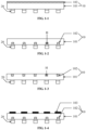
- the QD layer 102 may include a plurality of QD blocks. There are one-to-one correspondences between the plurality of QD blocks and the plurality of light emitting units 20. An orthographic projection of each of the plurality of QD blocks on the first surface of the light guide plate 10 is overlapped with an orthographic projection of a corresponding light emitting unit 20 on the first surface of the light guide plate 10. Compared with the backlight shown in Fig. 1-1 , the backlight shown in Fig. 1-2 may save the QD material and may lead to the reduction of the production cost.
- the orthographic projections of the QD blocks on the first surface of the light guide plate and the orthographic projections of the light emitting units on the first surface of the light guide plate are overlapped and correspond with one to one.
- the light emitted by the light emitting units may trigger the QD blocks to emit light in the scattering manner to achieve the light uniformization or light homogenization effect.
- the orthographic projections of the QD blocks on the first surface of the light guide plate may cover the orthographic projections of the light emitting units on the first surface of the light guide plate.
- the orthographic projections of the light emitting units on the first surface of the light guide plate may cover the orthographic projections of the QD blocks on the first surface of the light guide plate.
- the orthographic projections of the QD blocks on the first surface of the light guide plate may be completely overlapped with the orthographic projections of the light emitting units on the first surface of the light guide plate.
- the orthographic projections of the QD blocks on the first surface of the light guide plate may be partially overlapped with the orthographic projections of the light emitting units on the first surface of the light guide plate.
- Other situations between the two may be arranged and will not be elaborated herein but should be still in the scope of the present disclosure.
- a plurality of cavities H may be formed in the surface of the light guide plate body 101, and a QD block may be arranged to place in each of the plurality of cavities H.
- the plurality of cavities H may be formed in a surface of the light guide plate body 101 in a format of an array.
- the plurality of cavities H arranged in the array may be formed in the first surface of the light guide plate 10.
- the plurality of cavities H formed in the array may be formed in the second surface of the light guide plate.
- the QD blocks may be arranged in the light guide plate body, and the thickness of the backlight may be reduced.
- a packaging adhesive may be applied on the surfaces of the QD blocks.
- an integrated packaging adhesive layer may be developed on the surface, in which the cavities are formed, of the light guide plate body.
- a layer of packaging adhesive may be coated on the surface of each of the plurality of QD blocks in the cavities to seal the QD block.
- an edge of the QD layer in the backlight shown in Fig. 1-1 may be easily corroded by the water oxygen in the air. As such, a failure of the QD material on the edge may occur and may affect the light emitting quality of the backlight to a certain extent.
- the QD blocks in the backlight shown in Fig. 1-2 and 1-3 are well sealed, so that the problem of failure of the edge can be solved.
- the plurality of cavities H may be arranged in the array and may be formed in the first surface of the light guide plate 10.
- the light guide plate 10 further includes: a plurality of reflectors 103 that are arranged on the light emitting surface of the light guide plate body 101.
- the plurality of QD blocks may have one reflector that is associated with it, and the size of the reflector may be equal or greater than the cavity that contain the QD block.
- both the reflector and the outside edge of the cavity that contains the QD block have substantial round shapes and may have the equal size with diameter of 250 um. As such, the reflector and QD b block may not be recognizable by human eyes.
- an orthographic projection of each of the plurality of reflectors 103 on the first surface of the light guide plate 10 covers the orthographic projection of a corresponding QD block on the first surface of the light guide plate 10 and a reflecting surface of each of the plurality of reflectors faces a corresponding QD block.
- the reflectors may reflect the scattered light emitted by the QD blocks into the light guide plate body to continuously transmit the light in the light guide plate 10.
- the light may be better uniformized or homogenized, and the optical quality of the backlight may be improved.
- the plurality of reflectors may form a diffuse reflection array on the light emitting surface of the light guide plate body, and the reflecting surfaces of the reflectors may be concave surfaces.
- Such reflectors may increase a ratio of light that achieves total internal reflection and may thus increase the utilization rate of the light.
- the backlight may further include: an optical film layer 30 that is positioned on the light emitting surface side of the light guide plate 10.
- the optical film layer may include a brightness enhancement film and a diffusion film.
- coupling structures may be adopted to regulate the emitting light of the backlight.
- the coupling structures may form an integrated structure with the light guide plate, or may be separated from the light guide plate to form independent structures.
- An implementable arrangement manner for the coupling structures may include the following aspects.
- coupling structures 301 may be arranged on the side, which is away from the light guide plate 10, of the optical film layer 30.
- the gaps between the plurality of reflectors 103 in the middle of the optical film layer 30 and the light guide plate body 101 may be filled with the transparent adhesive 13.
- a refractive index t0 of the transparent adhesive may meet: t1 ⁇ t0 ⁇ t2, where t1 represents a refractive index of the light guide plate, and t2 represents a refractive index of the optical film layer.
- the transparent adhesive is filled between the optical film layer and the light guide plate body.
- the refractive index of the transparent adhesive is ensured to be more than or equal to the refractive index of the light guide plate and less than or equal to the refractive index of the optical film layer. In such way, the light is always transmitted from an optically thinner medium to an optically denser medium in the process of transmitting the light to the optical film via the light guide plate. Thus, a part of light may be effectively prevented from total reflection during transmission, and the utilization of the light may be increased.
- the coupling structures form the integrated structure with the light guide plate
- the light guide plate 10 may include: coupling structures 104 that are arranged on a surface of the light guide plate body 101.
- the coupling structures 104 may be arranged on the light emitting surface of the light guide plate body 101 and between every two adjacent reflectors 103.
- the coupling structures 104 may be arranged on the first surface of the light guide plate body 101 and the coupling structures 104 may be arranged between adjacent QD blocks 102..
- the coupling structures may have one of lattice point structures, grating structures, micro-lens structures and micro-prism structures.
- grating parameters such as a grating constant, a cavity depth, a duty ratio, a grating line direction may be set to control a wavelength, direction and efficiency of light coupled from the grating structures.
- the three-dimensional (3D) displaying, peep-proof displaying and the like may further be implemented through the backlight.
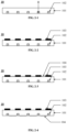
- the embodiment of the present disclosure provides two array structures of the light emitting units, including a first array structure and a second array structure.
- the first array structure of the light emitting units is shown in Fig. 1-8 .
- the backlight may further include a substrate 40.
- the plurality of light emitting units 20 may be fixed on a surface of the substrate 40.
- the light emitting surfaces of the plurality of light emitting units may be attached onto the first surface of the light guide plate 10. Because, in this implementation, a shorter distance is required for light mixing, and the backlight may be thinner. In the embodiment of the present disclosure, the light emitting surfaces of the light emitting units may be attached onto the first surface of the light guide plate.
- the thickness of the backlight may be effectively reduced, and the lightness and thinness of the backlight can be improved.
- the substrate 40 may be a transparent substrate.
- a reflecting layer 401 may be arranged on the other surface of the substrate.
- the other surface of the substrate is in the opposite side where the LEDs are placed.
- the reflecting layer 401 may reflect light escaping from the light guide plate back to the light guide plate and the utilization rate of the light can be increased.
- the reflecting layer 401 may be formed on the other surface of the substrate by coating a reflecting material such as silver or aluminium. And then, a protective layer is coated on the reflecting layer to protect the reflecting material. Alternatively, a reflecting film may be attached onto the other surface of the substrate.
- a second array structure of the light emitting units is shown in Fig. 1-9 .
- the plurality of light emitting units 20 may be bonded onto the first surface of the light guide plate 10.
- the light emitting units may be micro light emitting chips, such as micro blue LEDs. The size of the micro light emitting chips are relatively smaller.
- the whole or part of a micro light emitting chip array may be conveniently bonded with a driving substrate.
- a driving circuit may be arranged on the first surface of the light guide plate, and the light guide plate may be adopted as the driving substrate.
- the plurality of light emitting units may be bonded onto the first surface of the light guide plate in a welding manner. A process for such a structure is low in difficulty and is relatively lower in cost.
- the driving circuit may be arranged on the first surface of the light guide plate as shown in Fig. 1-9 .
- the coupling structures are usually not arranged on the first surface of the light guide plate.
- the coupling structures 104 may alternatively be arranged on an emitting side of the optical film layer as shown in Fig. 1-9 .
- a reflecting layer 105 may be arranged to place in an area other than the area where the light emitting units 20 are placed on the first surface of the light guide plate 10.
- the reflecting layer may reflect light received on the first surface of the light guide plate back to the light guide plate. The utilization rate of the light can thus be increased.
- the reflecting layer may be formed on the first surface of the light guide plate in the manner of coating the reflecting material such as silver or aluminium.
- the micro light emitting chips may be bonded onto the first surface of the light guide plate.
- the reflecting layer may be arranged to place in the area other than the area where the light emitting units are positioned on the first surface of the light guide plate. Because no substrate is required, the thickness of the backlight may further be reduced.
- the light emitting units arranged in the array may be controlled by an independent control unit as to whether to emit light or not.
- the area light control may thus be achieved.
- the light emitting units may be LEDs.
- the light emitting units in the embodiment of the present disclosure may be blue LEDs.
- the light emitting units may be micro blue LEDs. The blue LEDs may effectively trigger the QD layer to emit light in the scattering manner.
- the QD layer may be made from a QD material which may include a base material, a ligand material and scattering particles.
- the base material may include polyetherimide (PEI) and ammonium persulfate (APS).
- the ligand material may include an epoxy resin.
- the scattering particles may include silicon dioxide particles.
- the base material and the ligand material may mitigate the impact on QDs from an environment of high temperature, high-intensity light, water and oxygen. The scattering particles may facilitate the light emitted by the QDs to scatter around.
- the QDs may be cadmium selenide QDs.
- Fig. 1-10 is a schematic diagram of light transmission of a backlight shown in Fig. 1-8 .
- a part of light in the scattered light emitted by the QDs is transmitted to a far end in the light guide plate body 101, the other part of light is reflected by the reflectors 103.
- a part of light in the light reflected by the reflectors 103 is transmitted to the far end in the light guide plate body 101, the other part of light may be reflected by the reflecting layer 401 back into the light guide plate for transmission after escaping from the light guide plate.
- the light transmitted to the far end may be regulated through the coupling structures 104.
- Such a backlight may well uniformize the light, and may also effectively increase the utilization rate of the light.
- the backlight is the direct type backlight, and includes the light guide plate and the plurality of light emitting units arranged on the first surface of the light guide plate.
- the QD layer is arranged on the light guide plate, and the QD layer may be triggered by the light emitting units to emit the light in the scattering manner to achieve the light uniformization effect.
- the light emitting sides of the light emitting units are not required to be formed a certain distance from the first surface of the light guide plate for mixing light.
- the light emitting units may be attached onto the first surface of the light guide plate.
- the whole structure of the backlight may be prevented from being limited by the distance between the light emitting units and the light guide plate for achieving the light uniformization.
- the ability to flexibly adjust the backlight is improved, and attachment arrangement of the light emitting surfaces of the light emitting units and the first surface of the light guide plate also improves the lightness and thinness of the backlight.
- the light guide plate 10 may include: a light guide plate body 101 and a plurality of QD blocks 102 arranged on the light guide plate body 101.
- a plurality of cavities H are formed in a surface of the light guide plate body 101, and a QD block is arranged in each of the plurality of cavities.
- the plurality of cavities H are formed in a surface of the light guide plate body 101 in an array.
- the plurality of cavities H arranged in the array may be formed in a first surface of the light guide plate 10, or in a light emitting surface of the light guide plate 10.
- the cavities are formed in a surface of the light guide plate body, a QD block may be arranged in each of the plurality of cavities.
- the light may trigger the QD blocks to emit light in a scattering manner after entering the light guide plate, and a light uniformization effect of the light guide plate may be improved comparing with other implementations.
- a light guide plate 10 further includes: a plurality of reflectors 103 arranged on the light emitting surface of the light guide plate body 101. There is a one-to-one correspondences between each of the plurality of QD blocks 102 and each of the plurality of reflectors 103.
- an orthographic projection of each of the plurality of reflectors 103 on the first surface of the light guide plate 10 covers an orthographic projection of a corresponding QD block on the first surface of the light guide plate.
- a reflecting surface of each of the plurality of reflectors faces and is associated with a corresponding QD block.
- the reflectors reflect the scattered light emitted by the QD blocks into the light guide plate body to continue transmitting the light in the light guide plate.
- the light uniformization effect of the light guide plate may be improved, and optical quality of a backlight may further be improved.
- the plurality of reflectors may form a diffuse reflection array on the light emitting surface of the light guide plate body.
- the reflecting surfaces of the reflectors may be concave surfaces so that the reflectors may increase a ratio of light to generate the total internal reflection and may increase the utilization rate of the light.
- the light guide plate 10 may further include: grating structures 104 that may be arranged on a surface of the light guide plate body 101.
- the grating structures 104 may be arranged on the light emitting surface of the light guide plate body 101 and the grating structures 104 may be arranged between adjacent reflectors 103.
- the grating structures 104 may alternatively be arranged on the first surface of the light guide plate 101 and the grating structures 104 may be arranged between adjacent QD blocks 102.
- Grating parameters such as a grating constant, a cavity depth, a duty ratio and a grating line direction may be set to control a wavelength, direction and efficiency of light coupled from the grating structures. Further, the 3D displaying, peep-proof displaying and the like may further be implemented through the backlight.
- the grating structures may belong to coupling structures, and may be used for regulating emitting light of the backlight.
- the coupling structures arranged on a surface of the light guide plate body may further include: lattice point structures, micro-lens structures or micro-prism structures.
- the QD blocks are made from the QD material which may include a base material, a ligand material and scattering particles.
- the base material may include PEI and APS.
- the ligand material may include an epoxy resin.
- the scattering particles may include silicon dioxide particles.
- the base material and the ligand material may reduce the impact on QDs due to of an environment of high temperature, high-intensity light, water, oxygen and the light.
- the scattering particles may facilitate the light emitted by the QDs to scatter around.
- the QDs may be cadmium selenide QDs.
- a packaging adhesive 102a may be arranged on the plurality of QD blocks 102.
- a packaging adhesive layer 102a may be arranged on the whole surface, in which the cavities H are formed, of the light guide plate body 101.
- a layer of packaging adhesive 102a may merely be coated on the surfaces of the QD blocks in the cavities.
- the grating structures 104 may be arranged on the first surface of the light guide plate body 101.
- Fig. 2-4 is provided for exemplary description and is not intended to limit specific positions of the grating structures.
- the packaging adhesive is arranged on the QD blocks so that a good sealing effect on the QD blocks in the cavities may be achieved. The service life of the light guide plate may also be increased.
- a light guide plate structure provided by the embodiment of the present disclosure may refer to a light guide plate structure in a backlight in the abovementioned embodiment of the present disclosure, and will not be elaborated in the embodiment of the present disclosure.
- the cavities are formed in a surface of the light guide plate body, a QD block is arranged in each of the plurality of cavities, and the light may emitted from LEDs may trigger the QD blocks to emit the light in the scattering manner after entering the light guide plate so that the light uniformization effect of the light guide plate may be improved.
- An embodiment of the present disclosure provides a method for manufacturing a backlight as defined in appended claim 13.
- the backlight is a direct type backlight.
- the method may inter alia include the following steps.
- a light guide plate is manufactured where the light guide plate may include a light guide plate body and a QD layer that is arranged on the light guide plate body.
- a plurality of light emitting units are arranged on a first surface of the light guide plate.
- the light emitted by the plurality of light emitting units is capable of illuminating the QD layer to cause the QD layer to emit light.
- the backlight is the direct type backlight, and includes the light guide plate and the plurality of light emitting units arranged on the first surface of the light guide plate.
- the QD layer is arranged on the light guide plate, and may be excited by the light emitted from the light emitting units to emit light in a scattering manner to achieve a light uniformization effect.
- light emitting sides of the light emitting units are not required to allow a certain distance from the first surface of the light guide plate for mixing light.
- the light emitting units may be attached onto the first surface of the light guide plate.
- the structure of the backlight may be prevented from being limited by the distance between the light emitting units and the light guide plate for achieving light uniformization. The flexibility of regulation of the backlight is improved.
- the method for manufacturing the light guide plate includes the following steps.
- the light guide plate body is provided.
- a material of the light guide plate body may be an organic material or glass. Other materials may also be used and the present disclosure does not intend to limit the use of materials.
- a plurality of cavities are formed in a surface of the light guide plate body.
- the plurality of cavities H may be arranged in a surface of the light guide plate body 101 in an array.
- the plurality of cavities H arranged in the array may be formed in the first surface of the light guide plate 10.
- the plurality of cavities H formed in the array may alternatively be formed in a light emitting surface of the light guide plate 10.
- the plurality of cavities may be formed in a surface of the light guide plate body in a laser irradiation manner.
- the plurality of cavities may be formed in a surface of the light guide plate body by a one-time pattern construction process.
- the process may include the following steps.
- a mask pattern is formed on the light guide plate body.
- the mask pattern includes a plurality of hollow areas.
- a photoresist layer may be coated on the light guide plate body, and then the photoresist is exposed and is developed to obtain the mask pattern.
- a step S2 the light guide plate body formed with the mask pattern is etched to form one cavity in each of hollow areas in the light guide plate body.
- a step S3 the mask pattern is stripped.
- the cavities may be formed in the light guide plate body by adopting a wet etching process or a mechanical perforating method.
- a manner for forming the plurality of cavities in a surface of the light guide plate body may have many variations. The present disclosure does not intend to limit to any specific manner.
- each of the plurality of cavities is filled with the QD material to form a plurality of QD blocks.
- a method for filling each of the plurality of cavities with the QD material to form the plurality of QD blocks may include: Filling each of the plurality of cavities with the QD material; and performing heat curing treatment on the QD material to form the plurality of QD blocks.
- the QD material may include a base material, a ligand material and scattering particles.
- the base material may include PEI and APS.
- the ligand material may include an epoxy resin.
- the scattering particles may include silicon dioxide particles.
- the base material and the ligand material may reduce the impact on QDs due to an environment of high temperature, high-intensity light, water, oxygen and the light.
- the scattering particles may facilitate the light emitted by the QDs to scatter around.
- the QDs may be cadmium selenide QDs.
- temperature during heat curing treatment of the QD material should be lower than 200 DEG C to avoid influence on light emitting performance of the QDs at high temperature and to avoid incapability in achievement of a curing effect on the QD material at low temperature.
- the heating temperature for heat curing treatment may be 100 DEG C.
- a packaging adhesive is coated on surfaces of the plurality of QD blocks.
- an integrated packaging adhesive layer may be arranged on the surface, in which the cavities H are formed, of the light guide plate body 101.
- a layer of packaging adhesive is coated on the surfaces of the QD blocks in the cavities.
- the packaging adhesive may be arranged on the QD blocks so that a good sealing effect on the QD blocks in the cavities may be achieved.
- the service life of the light guide plate may be prolonged.
- the present disclosure does not intend to limit the implementation of packaging adhesive.
- grating structures 104 may also be arranged on the light-emitting surface of the light guide plate body 101.
- Fig. 2-6 is provided for exemplary description and the present disclosure does not intend to limit specific positions of the grating structures.
- grating structures are formed on a surface of the light guide plate body in a transfer print manner.
- the grating structures may be formed on a surface of the light guide plate body in a nanoimprint manner.
- the grating structures may belong to coupling structures, and may be used for regulating emitting light of the backlight.
- the coupling structures arranged on a surface of the light guide plate body may further include: lattice point structures, micro-lens structures or micro-prism structures. The present disclosure does not intend to limit the implementations of coupling structures.
- the backlight may include the light guide plate and the plurality of light emitting units arranged on the first surface of the light guide plate.
- the QD layer is arranged on the light guide plate, and may be excited or triggered by the light emitted from the light emitting units to emit light in the scattering manner to achieve the light uniformization effect.
- the light emitting sides of the light emitting units are not required to be formed with a certain distance from the first surface of the light guide plate for light mixing.
- the light emitting units may be attached onto the first surface of the light guide plate.
- the structure of the backlight may be prevented from being limited by the distance between the light emitting units and the light guide plate for achieving light uniformization.
- the flexibility to regulate the backlight is improved.
- the attachment arrangement of the light emitting surfaces of the light emitting units and the first surface of the light guide plate also improves lightness and thinness of the backlight.
- An embodiment of the present invention provides a method for manufacturing a light guide plate. As shown in Fig. 4 , the method includes the following steps.
- a step 601 providing a main body of plate shape.
- a step 602 forming a plurality of cavities in a surface of the light guide plate body.
- a step 603 filling each of the plurality of cavities with the QD material to form a plurality of QD blocks.
- the cavities are formed in a surface of the light guide plate body, a QD block is arranged in each of the plurality of cavities, and light may excite the QD blocks to emit light in a scattering manner after entering the light guide plate.
- a light uniformization effect of the light guide plate may be improved.
- An embodiment of the present invention provides a display device, which may include: any backlight shown in Fig. 1-4 to Fig. 1-9 .
- the display device provided by the embodiment of the present invention may be any product or part with a displaying function such as a mobile phone, a tablet computer, a television, a display, a notebook computer, a digital photo frame and a navigator.
- a displaying function such as a mobile phone, a tablet computer, a television, a display, a notebook computer, a digital photo frame and a navigator.
- the display device provided by the embodiment of the present invention includes a direct type backlight
- the direct type backlight includes a light guide plate and a plurality of light emitting units arranged on a first surface of the light guide plate.
- a QD layer is arranged on the light guide plate, and the QD layer may be excited or triggered by light emitted from the light emitting units to emit light in a scattering manner to achieve a light uniformization effect.
- light emitting sides of the light emitting units are not required to be formed with a certain distance from the first surface of the light guide plate for light mixing.
- they may be attached onto the first surface of the light guide plate.
- the whole structure of the backlight may be prevented from being limited by the distance between the light emitting units and the light guide plate for the sake of light uniformization. The flexibility to regulate the backlight is improved.
Landscapes
- Physics & Mathematics (AREA)
- Nonlinear Science (AREA)
- General Physics & Mathematics (AREA)
- Optics & Photonics (AREA)
- Mathematical Physics (AREA)
- Chemical & Material Sciences (AREA)
- Crystallography & Structural Chemistry (AREA)
- Planar Illumination Modules (AREA)
- Light Guides In General And Applications Therefor (AREA)
Claims (14)
- Lichtleiterplatte (10), umfassend:einen Hauptkörper (101), der eine Plattenform aufweist,eine Vielzahl von Hohlräumen (H) auf einer ersten Fläche des Hauptkörpers (101), und wobei die erste Fläche eine Hauptfläche des Hauptkörpers (101) ist, undeine Vielzahl von Quantenpunkt(Quantum Dot - QD)-Blöcken (102) auf dem Hauptkörper (101),wobei jeder der Vielzahl von Hohlräumen (H) mit einem der Vielzahl von QD-Blöcken (102) derart gefüllt ist, dass die erste Fläche eben ist, unddadurch gekennzeichnet, dass die Lichtleiterplatte (10) ferner Folgendes umfasst:eine Vielzahl von Reflektoren (103), die auf einer zweiten Fläche des Hauptkörpers (101) angeordnet ist, wobei die zweite Fläche eine Hauptfläche des Hauptkörpers gegenüber der ersten Fläche ist,wobei eine Eins-zu-Eins-Übereinstimmung zwischen der Vielzahl von QD-Blöcken (102) und der Vielzahl von Reflektoren (103) besteht,wobei eine senkrechte Projektion jedes der Vielzahl von Reflektoren (103) auf der ersten Fläche des Hauptkörpers (101) eine senkrechte Projektion eines entsprechenden QD-Blocks (102) auf der ersten Fläche des Hauptkörpers (101) bedeckt und eine reflektierende Fläche jedes der Vielzahl von Reflektoren (103) einem entsprechenden QD-Block (102) zugewandt ist.
- Lichtleiterplatte (10) nach Anspruch 1, ferner umfassend:
Gitterstrukturen, die auf einer der Vielzahl von Flächen des Hauptkörpers (101) angeordnet sind. - Lichtleiterplatte (10) nach Anspruch 1, wobei die QD-Blöcke (102) aus einem QD-Material bestehen, das ein Basismaterial, ein Ligandmaterial und Streupartikel umfasst; und das Basismaterial Polyetherimid (PEI) und Ammoniumpersulfat (APS) umfasst, das Ligandmaterial ein Epoxidharz umfasst und die Streupartikel Siliziumdioxidpartikel umfassen;
wobei die Lichtleiterplatte (10) optional ferner Folgendes umfasst:
eine Verpackungsklebstoffschicht (102a) auf der Vielzahl von QD-Blöcken (102). - Rückbeleuchtung eines Direkttyps, umfassend:die Lichtleiterplatte nach Anspruch 1; undeine Vielzahl von lichtemittierenden Einheiten (20), die zu einer Seite hin platziert ist, wo sich die erste Fläche der Lichtleitplatte (10) befindet; wobeijede der Vielzahl von lichtemittierenden Einheiten (20) eine lichtemittierende Fläche aufweist, die auf der ersten Fläche der Lichtleiterplatte (10) angebracht ist;die Vielzahl von Quantenpunktblöcken (102) eine Quantenpunkt(QD)-Schicht auf der ersten Fläche des Hauptkörpers (101) bildet und die erste Fläche eine Lichteintrittsfläche des Hauptkörpers (101) ist; unddas durch die Vielzahl von lichtemittierenden Einheiten (20) emittierte Licht in der Lage ist, die QD-Schicht zu beleuchten, um zu bewirken, dass die QD-Schicht Licht emittiert.
- Rückbeleuchtung nach Anspruch 4, wobei
eine senkrechte Projektion jedes der Vielzahl von QD-Blöcken (102) auf der ersten Fläche mit einer senkrechten Projektion mindestens einer der Vielzahl von lichtemittierenden Einheiten (20) auf der ersten Fläche überlappt. - Rückbeleuchtung nach Anspruch 5, wobei die zweite Fläche im Wesentlichen eben ist.
- Rückbeleuchtung nach Anspruch 4, ferner umfassend:eine optische Filmschicht (30) auf einer Seite der Lichtleiterplatte (10), die von der Vielzahl von lichtemittierenden Einheiten (20) weg platziert ist;Koppelstrukturen (301) auf einer Seite der optischen Filmschicht (30), die von der Lichtleiterplatte (10) entfernt sind;eine transparente Klebstoffschicht (13) zwischen der optischen Filmschicht (30) und der Lichtleiterplatte (10); undeinen Brechungsindex t0 des transparenten Klebstoffs (13), der größer als ein Brechungsindex t1 der Lichtleiterplatte (10) und kleiner als ein zweiter Brechungsindex t2 der optischen Filmschicht (30) ist.
- Rückbeleuchtung nach Anspruch 6 oder 7, wobei die Lichtleiterplatte (10) ferner Folgendes umfasst:
Koppelstrukturen (104), die auf einer von der ersten Fläche und der zweiten ebenen Fläche angeordnet sind. - Rückbeleuchtung nach Anspruch 7 oder 8, wobei die Koppelstrukturen (104; 301) Gitterpunktstrukturen, Gitterstrukturen, Mikrolinsenstrukturen oder Mikroprismenstrukturen sind.
- Rückbeleuchtung nach Anspruch 4, ferner umfassend ein Substrat (40), wobeidie Vielzahl von lichtemittierenden Einheiten (20) auf einer Fläche des Substrats (40) befestigt ist;das Substrat (40) optional ein transparentes Substrat ist und eine reflektierende Schicht auf einer zweiten Fläche des Substrats (40) angeordnet ist.
- Rückbeleuchtung nach Anspruch 4, wobei die lichtemittierenden Einheiten (20) lichtemittierende Mikrochips sind und die Vielzahl von lichtemittierenden Einheiten (20) auf die erste Fläche des Hauptkörpers (101) gebondet ist;
wobei die Rückbeleuchtung optional ferner Folgendes umfasst:
eine reflektierende Schicht, die die erste Fläche bedeckt, außer an der Stelle, an der die lichtemittierenden Einheiten (20) positioniert sind. - Rückbeleuchtung nach Anspruch 4, wobei die lichtemittierenden Einheiten (20) blaue Leuchtdioden (LED) sind; die Vielzahl von QD-Blöcken (102) optional aus einem QD-Material besteht, das ein Basismaterial, ein Ligandmaterial und Streupartikel umfasst; und
das Basismaterial Polyetherimid (PEI) und Ammoniumpersulfat (APS) umfasst, das Ligandmaterial ein Epoxidharz umfasst und die Streupartikel Siliziumdioxidpartikel umfassen. - Verfahren zum Herstellen einer Lichtleiterplatte (10), umfassend:Bereitstellen (501) eines Hauptkörpers, der eine Plattenform aufweist;Bilden einer Vielzahl von Hohlräumen (H) auf einer ersten Fläche, die die Hauptfläche des Hauptkörpers (101) ist, undBereitstellen einer Vielzahl von Quantenpunkt(QD)-Blöcken auf dem Hauptkörper (101),wobei jeder der Vielzahl von Hohlräumen (H) einen der Vielzahl von QD-Blöcken (102) enthält,dadurch gekennzeichnet, dass das Verfahren ferner Folgendes umfasst:Bereitstellen einer Vielzahl von Reflektoren (103), wobei die Vielzahl von Reflektoren (103) auf einer zweiten Fläche des Hauptkörpers (101) angeordnet ist, wobei die zweite Fläche eine Hauptfläche des Hauptkörpers gegenüber der ersten Fläche ist, wobei eine Eins-zu-Eins-Übereinstimmung zwischen der Vielzahl von QD-Blöcken (102) und der Vielzahl von Reflektoren (103) besteht undwobei die senkrechte Projektion jedes der Vielzahl von Reflektoren (103) auf der ersten Fläche des Hauptkörpers (101) die senkrechte Projektion eines entsprechenden QD-Blocks (102) auf der ersten Fläche des Hauptkörpers (101) bedeckt und eine reflektierende Fläche jedes der Vielzahl von Reflektoren (103) einem entsprechenden QD-Block (102) zugewandt ist.
- Anzeigevorrichtung, umfassend:
die Rückbeleuchtung nach einem der Ansprüche 4-12.
Applications Claiming Priority (2)
| Application Number | Priority Date | Filing Date | Title |
|---|---|---|---|
| CN201710021787.3A CN108303819B (zh) | 2017-01-12 | 2017-01-12 | 背光源及其制造方法、导光板及其制造方法及显示装置 |
| PCT/CN2017/095586 WO2018129909A1 (en) | 2017-01-12 | 2017-08-02 | Backlight and manufacturing method thereof, light guide plate and manufacturing method thereof, and display device |
Publications (3)
| Publication Number | Publication Date |
|---|---|
| EP3568727A1 EP3568727A1 (de) | 2019-11-20 |
| EP3568727A4 EP3568727A4 (de) | 2020-06-24 |
| EP3568727B1 true EP3568727B1 (de) | 2024-03-06 |
Family
ID=62839219
Family Applications (1)
| Application Number | Title | Priority Date | Filing Date |
|---|---|---|---|
| EP17842314.1A Active EP3568727B1 (de) | 2017-01-12 | 2017-08-02 | Rückbeleuchtung und herstellungsverfahren dafür, lichtleiterplatte und herstellungsverfahren dafür und anzeigevorrichtung |
Country Status (5)
| Country | Link |
|---|---|
| US (1) | US10288939B2 (de) |
| EP (1) | EP3568727B1 (de) |
| JP (1) | JP7026612B2 (de) |
| CN (1) | CN108303819B (de) |
| WO (1) | WO2018129909A1 (de) |
Families Citing this family (17)
| Publication number | Priority date | Publication date | Assignee | Title |
|---|---|---|---|---|
| CN108983494A (zh) * | 2018-07-27 | 2018-12-11 | 惠州市华星光电技术有限公司 | 背光模组及其制作方法 |
| CN109031788A (zh) * | 2018-08-31 | 2018-12-18 | 青岛海信电器股份有限公司 | 一种背光模组及显示装置 |
| WO2021071378A1 (en) * | 2019-10-09 | 2021-04-15 | Corning Incorporated | Backlight including patterned reflectors, diffuser plate, and method for fabricating the backlight |
| WO2020214047A1 (en) * | 2019-04-15 | 2020-10-22 | Corning Incorporated | Backlight including patterned reflectors and method for fabricating the backlight |
| TW202036060A (zh) * | 2018-11-12 | 2020-10-01 | 美商康寧公司 | 包括圖案化反射器之背光、擴散板及製造背光之方法 |
| CN109358450B (zh) * | 2018-11-28 | 2023-12-01 | 武汉华星光电技术有限公司 | 薄型背光模组及其制作方法 |
| CN109557719B (zh) * | 2018-11-30 | 2021-07-27 | 合肥泰沃达智能装备有限公司 | 一种具有半反半透导光板的直下式零od背光结构 |
| CN110850637A (zh) * | 2019-11-29 | 2020-02-28 | 维沃移动通信有限公司 | 背光模组及电子设备 |
| CN115066649A (zh) * | 2020-02-10 | 2022-09-16 | 康宁公司 | 包含图案化反射器的背光 |
| TWI719852B (zh) * | 2020-03-05 | 2021-02-21 | 瑞軒科技股份有限公司 | 直下式背光裝置之加工系統及其加工方法 |
| CN111929949B (zh) * | 2020-08-18 | 2023-07-14 | 京东方科技集团股份有限公司 | Led背光结构 |
| KR102799420B1 (ko) * | 2020-10-20 | 2025-04-25 | 삼성전자주식회사 | 디스플레이 장치 |
| CN113741098B (zh) * | 2021-11-04 | 2022-03-01 | 拓米(成都)应用技术研究院有限公司 | 一种utg-qd型mini-led板及其应用、制备方法和光学架构 |
| CN113985659A (zh) | 2021-11-09 | 2022-01-28 | 广东粤港澳大湾区国家纳米科技创新研究院 | 一种量子点集成板、其制备方法及包含其的显示装置 |
| TWI803046B (zh) * | 2021-11-10 | 2023-05-21 | 李裕翔 | 導光薄膜 |
| TWI817323B (zh) * | 2022-01-17 | 2023-10-01 | 穎台科技股份有限公司 | 量子點光擴散板及其製法 |
| KR20260016059A (ko) * | 2024-07-26 | 2026-02-03 | 한국광기술원 | 마이크로 렌즈 어레이 모듈 및 그 제조방법 |
Family Cites Families (19)
| Publication number | Priority date | Publication date | Assignee | Title |
|---|---|---|---|---|
| US8459855B2 (en) * | 2008-07-28 | 2013-06-11 | Munisamy Anandan | UV LED based color pixel backlight incorporating quantum dots for increasing color gamut of LCD |
| CN101660719A (zh) * | 2008-08-29 | 2010-03-03 | 京东方科技集团股份有限公司 | 背光源模块 |
| JP5440064B2 (ja) * | 2008-10-21 | 2014-03-12 | 東芝ライテック株式会社 | 照明装置 |
| CN201437941U (zh) * | 2009-04-30 | 2010-04-14 | 达运精密工业(苏州)有限公司 | Led背光模组及液晶显示装置 |
| CN201715447U (zh) * | 2009-11-24 | 2011-01-19 | 金芃 | Led背光源的带有阵列式的反光物体的直下式导光板 |
| EP2638321B1 (de) * | 2010-11-10 | 2019-05-08 | Nanosys, Inc. | Quantenpunktfilme, beleuchtungsvorrichtungen und beleuchtungsverfahren |
| KR20120138080A (ko) * | 2011-06-14 | 2012-12-24 | 엘지이노텍 주식회사 | 발광 소자 |
| KR102132220B1 (ko) | 2013-12-27 | 2020-07-10 | 삼성디스플레이 주식회사 | 양자점 광학 소자의 제조 방법 및 양자점 광학 소자를 포함한 백라이트 유닛 |
| KR101657954B1 (ko) | 2014-02-05 | 2016-09-21 | 삼성디스플레이 주식회사 | 백라이트 어셈블리 및 이를 포함하는 표시 장치 |
| US9146419B1 (en) * | 2014-06-24 | 2015-09-29 | Munisamy Anandan | Quantum rod based color pixel backlight for LCD |
| CN104154468B (zh) | 2014-09-01 | 2016-08-31 | 深圳市华星光电技术有限公司 | 背光模组 |
| TWI581017B (zh) | 2014-09-30 | 2017-05-01 | 鴻海精密工業股份有限公司 | 顏色轉換膜、使用顏色轉換膜的顯示裝置及製造該顏色轉換膜的方法 |
| CN105044815A (zh) * | 2015-08-12 | 2015-11-11 | 深圳市华星光电技术有限公司 | 导光板和背光模组 |
| CN105158972A (zh) * | 2015-09-10 | 2015-12-16 | 深圳市华星光电技术有限公司 | 导光板及导光板的制备方法 |
| CN105319773A (zh) * | 2015-11-03 | 2016-02-10 | 青岛海信电器股份有限公司 | 一种背光模组和液晶显示设备 |
| CN105388666B (zh) | 2015-12-11 | 2019-01-01 | 青岛海信电器股份有限公司 | 背光模组及显示装置 |
| CN205388672U (zh) * | 2016-02-02 | 2016-07-20 | 陕西科技大学 | 一种基于量子点发光的显示器件 |
| US10754081B2 (en) * | 2016-03-07 | 2020-08-25 | Current Lighting Solutions, Llc | Devices containing a remote phosphor package with red line emitting phosphors and green emitting quantum dots |
| JP2019532481A (ja) * | 2016-09-07 | 2019-11-07 | コーニング インコーポレイテッド | 色変換導光板および色変換導光板を含む装置 |
-
2017
- 2017-01-12 CN CN201710021787.3A patent/CN108303819B/zh active Active
- 2017-08-02 US US15/745,043 patent/US10288939B2/en active Active
- 2017-08-02 EP EP17842314.1A patent/EP3568727B1/de active Active
- 2017-08-02 WO PCT/CN2017/095586 patent/WO2018129909A1/en not_active Ceased
- 2017-08-02 JP JP2018513281A patent/JP7026612B2/ja active Active
Also Published As
| Publication number | Publication date |
|---|---|
| US20190011780A1 (en) | 2019-01-10 |
| US10288939B2 (en) | 2019-05-14 |
| JP2020506496A (ja) | 2020-02-27 |
| CN108303819A (zh) | 2018-07-20 |
| EP3568727A4 (de) | 2020-06-24 |
| JP7026612B2 (ja) | 2022-02-28 |
| EP3568727A1 (de) | 2019-11-20 |
| WO2018129909A1 (en) | 2018-07-19 |
| CN108303819B (zh) | 2020-11-24 |
Similar Documents
| Publication | Publication Date | Title |
|---|---|---|
| EP3568727B1 (de) | Rückbeleuchtung und herstellungsverfahren dafür, lichtleiterplatte und herstellungsverfahren dafür und anzeigevorrichtung | |
| JP7125636B2 (ja) | 発光装置 | |
| JP5216212B2 (ja) | 発光デバイス | |
| CN104298001B (zh) | 直下式背光模组及其制造方法 | |
| JP6680349B1 (ja) | 発光モジュール | |
| TWI447450B (zh) | 導光板結構、背光模組及其製造方法 | |
| US10690834B2 (en) | Backlight device and manufacturing method thereof | |
| KR20120088273A (ko) | 백라이트 유닛 및 그 제조 방법 | |
| WO2019080536A1 (zh) | 背光模组、显示屏及终端 | |
| TW202009580A (zh) | 畫素陣列封裝結構及顯示面板 | |
| CN105867026A (zh) | 量子点光源器件、背光模组及液晶显示装置 | |
| US20210036198A1 (en) | Light-emitting unit and surface-emission light source | |
| JP7319557B2 (ja) | 発光モジュール | |
| US20180095329A1 (en) | Lighting device, display device, and television device | |
| TW201210086A (en) | Light distribution control device, light-emitting device using same, and method of producing light distribution control device | |
| GB2614126A (en) | Display substrate and display apparatus | |
| KR20120127077A (ko) | 색 변환 소자 및 그 제조 방법 | |
| TW202034541A (zh) | 發光裝置、發光模組及發光裝置之製造方法 | |
| CN111308778B (zh) | 背光单元及包括背光单元的显示装置 | |
| CN109426034A (zh) | 液晶显示装置 | |
| WO2016155115A1 (zh) | 导光板及具有该导光板的背光模块和液晶显示器 | |
| TW201910885A (zh) | 液晶顯示裝置 | |
| US11131879B2 (en) | Backlight module and applications thereof | |
| US20130070481A1 (en) | Linear light source apparatus | |
| KR20140038062A (ko) | 퀀텀 도트부가 구비된 발광 장치 |
Legal Events
| Date | Code | Title | Description |
|---|---|---|---|
| STAA | Information on the status of an ep patent application or granted ep patent |
Free format text: STATUS: UNKNOWN |
|
| STAA | Information on the status of an ep patent application or granted ep patent |
Free format text: STATUS: THE INTERNATIONAL PUBLICATION HAS BEEN MADE |
|
| PUAI | Public reference made under article 153(3) epc to a published international application that has entered the european phase |
Free format text: ORIGINAL CODE: 0009012 |
|
| STAA | Information on the status of an ep patent application or granted ep patent |
Free format text: STATUS: REQUEST FOR EXAMINATION WAS MADE |
|
| 17P | Request for examination filed |
Effective date: 20180227 |
|
| AK | Designated contracting states |
Kind code of ref document: A1 Designated state(s): AL AT BE BG CH CY CZ DE DK EE ES FI FR GB GR HR HU IE IS IT LI LT LU LV MC MK MT NL NO PL PT RO RS SE SI SK SM TR |
|
| AX | Request for extension of the european patent |
Extension state: BA ME |
|
| DAX | Request for extension of the european patent (deleted) | ||
| A4 | Supplementary search report drawn up and despatched |
Effective date: 20200525 |
|
| RIC1 | Information provided on ipc code assigned before grant |
Ipc: G02F 1/13357 20060101AFI20200516BHEP |
|
| STAA | Information on the status of an ep patent application or granted ep patent |
Free format text: STATUS: EXAMINATION IS IN PROGRESS |
|
| 17Q | First examination report despatched |
Effective date: 20210719 |
|
| GRAP | Despatch of communication of intention to grant a patent |
Free format text: ORIGINAL CODE: EPIDOSNIGR1 |
|
| STAA | Information on the status of an ep patent application or granted ep patent |
Free format text: STATUS: GRANT OF PATENT IS INTENDED |
|
| INTG | Intention to grant announced |
Effective date: 20231012 |
|
| GRAS | Grant fee paid |
Free format text: ORIGINAL CODE: EPIDOSNIGR3 |
|
| GRAA | (expected) grant |
Free format text: ORIGINAL CODE: 0009210 |
|
| STAA | Information on the status of an ep patent application or granted ep patent |
Free format text: STATUS: THE PATENT HAS BEEN GRANTED |
|
| AK | Designated contracting states |
Kind code of ref document: B1 Designated state(s): AL AT BE BG CH CY CZ DE DK EE ES FI FR GB GR HR HU IE IS IT LI LT LU LV MC MK MT NL NO PL PT RO RS SE SI SK SM TR |
|
| REG | Reference to a national code |
Ref country code: GB Ref legal event code: FG4D |
|
| REG | Reference to a national code |
Ref country code: CH Ref legal event code: EP |
|
| REG | Reference to a national code |
Ref country code: IE Ref legal event code: FG4D |
|
| REG | Reference to a national code |
Ref country code: DE Ref legal event code: R096 Ref document number: 602017079836 Country of ref document: DE |
|
| REG | Reference to a national code |
Ref country code: LT Ref legal event code: MG9D |
|
| PG25 | Lapsed in a contracting state [announced via postgrant information from national office to epo] |
Ref country code: LT Free format text: LAPSE BECAUSE OF FAILURE TO SUBMIT A TRANSLATION OF THE DESCRIPTION OR TO PAY THE FEE WITHIN THE PRESCRIBED TIME-LIMIT Effective date: 20240306 |
|
| REG | Reference to a national code |
Ref country code: NL Ref legal event code: MP Effective date: 20240306 |
|
| PG25 | Lapsed in a contracting state [announced via postgrant information from national office to epo] |
Ref country code: GR Free format text: LAPSE BECAUSE OF FAILURE TO SUBMIT A TRANSLATION OF THE DESCRIPTION OR TO PAY THE FEE WITHIN THE PRESCRIBED TIME-LIMIT Effective date: 20240607 |
|
| PG25 | Lapsed in a contracting state [announced via postgrant information from national office to epo] |
Ref country code: HR Free format text: LAPSE BECAUSE OF FAILURE TO SUBMIT A TRANSLATION OF THE DESCRIPTION OR TO PAY THE FEE WITHIN THE PRESCRIBED TIME-LIMIT Effective date: 20240306 Ref country code: RS Free format text: LAPSE BECAUSE OF FAILURE TO SUBMIT A TRANSLATION OF THE DESCRIPTION OR TO PAY THE FEE WITHIN THE PRESCRIBED TIME-LIMIT Effective date: 20240606 |
|
| PG25 | Lapsed in a contracting state [announced via postgrant information from national office to epo] |
Ref country code: ES Free format text: LAPSE BECAUSE OF FAILURE TO SUBMIT A TRANSLATION OF THE DESCRIPTION OR TO PAY THE FEE WITHIN THE PRESCRIBED TIME-LIMIT Effective date: 20240306 |
|
| PG25 | Lapsed in a contracting state [announced via postgrant information from national office to epo] |
Ref country code: RS Free format text: LAPSE BECAUSE OF FAILURE TO SUBMIT A TRANSLATION OF THE DESCRIPTION OR TO PAY THE FEE WITHIN THE PRESCRIBED TIME-LIMIT Effective date: 20240606 Ref country code: NO Free format text: LAPSE BECAUSE OF FAILURE TO SUBMIT A TRANSLATION OF THE DESCRIPTION OR TO PAY THE FEE WITHIN THE PRESCRIBED TIME-LIMIT Effective date: 20240606 Ref country code: LT Free format text: LAPSE BECAUSE OF FAILURE TO SUBMIT A TRANSLATION OF THE DESCRIPTION OR TO PAY THE FEE WITHIN THE PRESCRIBED TIME-LIMIT Effective date: 20240306 Ref country code: HR Free format text: LAPSE BECAUSE OF FAILURE TO SUBMIT A TRANSLATION OF THE DESCRIPTION OR TO PAY THE FEE WITHIN THE PRESCRIBED TIME-LIMIT Effective date: 20240306 Ref country code: GR Free format text: LAPSE BECAUSE OF FAILURE TO SUBMIT A TRANSLATION OF THE DESCRIPTION OR TO PAY THE FEE WITHIN THE PRESCRIBED TIME-LIMIT Effective date: 20240607 Ref country code: FI Free format text: LAPSE BECAUSE OF FAILURE TO SUBMIT A TRANSLATION OF THE DESCRIPTION OR TO PAY THE FEE WITHIN THE PRESCRIBED TIME-LIMIT Effective date: 20240306 Ref country code: ES Free format text: LAPSE BECAUSE OF FAILURE TO SUBMIT A TRANSLATION OF THE DESCRIPTION OR TO PAY THE FEE WITHIN THE PRESCRIBED TIME-LIMIT Effective date: 20240306 Ref country code: BG Free format text: LAPSE BECAUSE OF FAILURE TO SUBMIT A TRANSLATION OF THE DESCRIPTION OR TO PAY THE FEE WITHIN THE PRESCRIBED TIME-LIMIT Effective date: 20240306 |
|
| REG | Reference to a national code |
Ref country code: AT Ref legal event code: MK05 Ref document number: 1664116 Country of ref document: AT Kind code of ref document: T Effective date: 20240306 |
|
| PG25 | Lapsed in a contracting state [announced via postgrant information from national office to epo] |
Ref country code: SE Free format text: LAPSE BECAUSE OF FAILURE TO SUBMIT A TRANSLATION OF THE DESCRIPTION OR TO PAY THE FEE WITHIN THE PRESCRIBED TIME-LIMIT Effective date: 20240306 Ref country code: LV Free format text: LAPSE BECAUSE OF FAILURE TO SUBMIT A TRANSLATION OF THE DESCRIPTION OR TO PAY THE FEE WITHIN THE PRESCRIBED TIME-LIMIT Effective date: 20240306 |
|
| PG25 | Lapsed in a contracting state [announced via postgrant information from national office to epo] |
Ref country code: NL Free format text: LAPSE BECAUSE OF FAILURE TO SUBMIT A TRANSLATION OF THE DESCRIPTION OR TO PAY THE FEE WITHIN THE PRESCRIBED TIME-LIMIT Effective date: 20240306 |
|
| PG25 | Lapsed in a contracting state [announced via postgrant information from national office to epo] |
Ref country code: NL Free format text: LAPSE BECAUSE OF FAILURE TO SUBMIT A TRANSLATION OF THE DESCRIPTION OR TO PAY THE FEE WITHIN THE PRESCRIBED TIME-LIMIT Effective date: 20240306 |
|
| PG25 | Lapsed in a contracting state [announced via postgrant information from national office to epo] |
Ref country code: IS Free format text: LAPSE BECAUSE OF FAILURE TO SUBMIT A TRANSLATION OF THE DESCRIPTION OR TO PAY THE FEE WITHIN THE PRESCRIBED TIME-LIMIT Effective date: 20240706 |
|
| PG25 | Lapsed in a contracting state [announced via postgrant information from national office to epo] |
Ref country code: PT Free format text: LAPSE BECAUSE OF FAILURE TO SUBMIT A TRANSLATION OF THE DESCRIPTION OR TO PAY THE FEE WITHIN THE PRESCRIBED TIME-LIMIT Effective date: 20240708 Ref country code: SM Free format text: LAPSE BECAUSE OF FAILURE TO SUBMIT A TRANSLATION OF THE DESCRIPTION OR TO PAY THE FEE WITHIN THE PRESCRIBED TIME-LIMIT Effective date: 20240306 |
|
| PG25 | Lapsed in a contracting state [announced via postgrant information from national office to epo] |
Ref country code: CZ Free format text: LAPSE BECAUSE OF FAILURE TO SUBMIT A TRANSLATION OF THE DESCRIPTION OR TO PAY THE FEE WITHIN THE PRESCRIBED TIME-LIMIT Effective date: 20240306 Ref country code: EE Free format text: LAPSE BECAUSE OF FAILURE TO SUBMIT A TRANSLATION OF THE DESCRIPTION OR TO PAY THE FEE WITHIN THE PRESCRIBED TIME-LIMIT Effective date: 20240306 |
|
| PG25 | Lapsed in a contracting state [announced via postgrant information from national office to epo] |
Ref country code: AT Free format text: LAPSE BECAUSE OF FAILURE TO SUBMIT A TRANSLATION OF THE DESCRIPTION OR TO PAY THE FEE WITHIN THE PRESCRIBED TIME-LIMIT Effective date: 20240306 |
|
| PG25 | Lapsed in a contracting state [announced via postgrant information from national office to epo] |
Ref country code: PL Free format text: LAPSE BECAUSE OF FAILURE TO SUBMIT A TRANSLATION OF THE DESCRIPTION OR TO PAY THE FEE WITHIN THE PRESCRIBED TIME-LIMIT Effective date: 20240306 |
|
| PG25 | Lapsed in a contracting state [announced via postgrant information from national office to epo] |
Ref country code: SK Free format text: LAPSE BECAUSE OF FAILURE TO SUBMIT A TRANSLATION OF THE DESCRIPTION OR TO PAY THE FEE WITHIN THE PRESCRIBED TIME-LIMIT Effective date: 20240306 |
|
| PG25 | Lapsed in a contracting state [announced via postgrant information from national office to epo] |
Ref country code: SM Free format text: LAPSE BECAUSE OF FAILURE TO SUBMIT A TRANSLATION OF THE DESCRIPTION OR TO PAY THE FEE WITHIN THE PRESCRIBED TIME-LIMIT Effective date: 20240306 Ref country code: SK Free format text: LAPSE BECAUSE OF FAILURE TO SUBMIT A TRANSLATION OF THE DESCRIPTION OR TO PAY THE FEE WITHIN THE PRESCRIBED TIME-LIMIT Effective date: 20240306 Ref country code: RO Free format text: LAPSE BECAUSE OF FAILURE TO SUBMIT A TRANSLATION OF THE DESCRIPTION OR TO PAY THE FEE WITHIN THE PRESCRIBED TIME-LIMIT Effective date: 20240306 Ref country code: PT Free format text: LAPSE BECAUSE OF FAILURE TO SUBMIT A TRANSLATION OF THE DESCRIPTION OR TO PAY THE FEE WITHIN THE PRESCRIBED TIME-LIMIT Effective date: 20240708 Ref country code: PL Free format text: LAPSE BECAUSE OF FAILURE TO SUBMIT A TRANSLATION OF THE DESCRIPTION OR TO PAY THE FEE WITHIN THE PRESCRIBED TIME-LIMIT Effective date: 20240306 Ref country code: IS Free format text: LAPSE BECAUSE OF FAILURE TO SUBMIT A TRANSLATION OF THE DESCRIPTION OR TO PAY THE FEE WITHIN THE PRESCRIBED TIME-LIMIT Effective date: 20240706 Ref country code: EE Free format text: LAPSE BECAUSE OF FAILURE TO SUBMIT A TRANSLATION OF THE DESCRIPTION OR TO PAY THE FEE WITHIN THE PRESCRIBED TIME-LIMIT Effective date: 20240306 Ref country code: CZ Free format text: LAPSE BECAUSE OF FAILURE TO SUBMIT A TRANSLATION OF THE DESCRIPTION OR TO PAY THE FEE WITHIN THE PRESCRIBED TIME-LIMIT Effective date: 20240306 Ref country code: AT Free format text: LAPSE BECAUSE OF FAILURE TO SUBMIT A TRANSLATION OF THE DESCRIPTION OR TO PAY THE FEE WITHIN THE PRESCRIBED TIME-LIMIT Effective date: 20240306 |
|
| PG25 | Lapsed in a contracting state [announced via postgrant information from national office to epo] |
Ref country code: IT Free format text: LAPSE BECAUSE OF FAILURE TO SUBMIT A TRANSLATION OF THE DESCRIPTION OR TO PAY THE FEE WITHIN THE PRESCRIBED TIME-LIMIT Effective date: 20240306 |
|
| REG | Reference to a national code |
Ref country code: DE Ref legal event code: R097 Ref document number: 602017079836 Country of ref document: DE |
|
| PG25 | Lapsed in a contracting state [announced via postgrant information from national office to epo] |
Ref country code: IT Free format text: LAPSE BECAUSE OF FAILURE TO SUBMIT A TRANSLATION OF THE DESCRIPTION OR TO PAY THE FEE WITHIN THE PRESCRIBED TIME-LIMIT Effective date: 20240306 |
|
| PLBE | No opposition filed within time limit |
Free format text: ORIGINAL CODE: 0009261 |
|
| STAA | Information on the status of an ep patent application or granted ep patent |
Free format text: STATUS: NO OPPOSITION FILED WITHIN TIME LIMIT |
|
| PG25 | Lapsed in a contracting state [announced via postgrant information from national office to epo] |
Ref country code: DK Free format text: LAPSE BECAUSE OF FAILURE TO SUBMIT A TRANSLATION OF THE DESCRIPTION OR TO PAY THE FEE WITHIN THE PRESCRIBED TIME-LIMIT Effective date: 20240306 |
|
| PG25 | Lapsed in a contracting state [announced via postgrant information from national office to epo] |
Ref country code: DK Free format text: LAPSE BECAUSE OF FAILURE TO SUBMIT A TRANSLATION OF THE DESCRIPTION OR TO PAY THE FEE WITHIN THE PRESCRIBED TIME-LIMIT Effective date: 20240306 |
|
| 26N | No opposition filed |
Effective date: 20241209 |
|
| REG | Reference to a national code |
Ref country code: CH Ref legal event code: PL |
|
| PG25 | Lapsed in a contracting state [announced via postgrant information from national office to epo] |
Ref country code: LU Free format text: LAPSE BECAUSE OF NON-PAYMENT OF DUE FEES Effective date: 20240802 |
|
| GBPC | Gb: european patent ceased through non-payment of renewal fee |
Effective date: 20240802 |
|
| PG25 | Lapsed in a contracting state [announced via postgrant information from national office to epo] |
Ref country code: CH Free format text: LAPSE BECAUSE OF NON-PAYMENT OF DUE FEES Effective date: 20240831 Ref country code: SI Free format text: LAPSE BECAUSE OF FAILURE TO SUBMIT A TRANSLATION OF THE DESCRIPTION OR TO PAY THE FEE WITHIN THE PRESCRIBED TIME-LIMIT Effective date: 20240306 Ref country code: MC Free format text: LAPSE BECAUSE OF FAILURE TO SUBMIT A TRANSLATION OF THE DESCRIPTION OR TO PAY THE FEE WITHIN THE PRESCRIBED TIME-LIMIT Effective date: 20240306 |
|
| REG | Reference to a national code |
Ref country code: BE Ref legal event code: MM Effective date: 20240831 |
|
| PG25 | Lapsed in a contracting state [announced via postgrant information from national office to epo] |
Ref country code: GB Free format text: LAPSE BECAUSE OF NON-PAYMENT OF DUE FEES Effective date: 20240802 |
|
| PG25 | Lapsed in a contracting state [announced via postgrant information from national office to epo] |
Ref country code: BE Free format text: LAPSE BECAUSE OF NON-PAYMENT OF DUE FEES Effective date: 20240831 |
|
| PG25 | Lapsed in a contracting state [announced via postgrant information from national office to epo] |
Ref country code: FR Free format text: LAPSE BECAUSE OF NON-PAYMENT OF DUE FEES Effective date: 20240831 |
|
| PG25 | Lapsed in a contracting state [announced via postgrant information from national office to epo] |
Ref country code: IE Free format text: LAPSE BECAUSE OF NON-PAYMENT OF DUE FEES Effective date: 20240802 |
|
| PGFP | Annual fee paid to national office [announced via postgrant information from national office to epo] |
Ref country code: DE Payment date: 20250820 Year of fee payment: 9 |
|
| PG25 | Lapsed in a contracting state [announced via postgrant information from national office to epo] |
Ref country code: CY Free format text: LAPSE BECAUSE OF FAILURE TO SUBMIT A TRANSLATION OF THE DESCRIPTION OR TO PAY THE FEE WITHIN THE PRESCRIBED TIME-LIMIT; INVALID AB INITIO Effective date: 20170802 |
|
| PG25 | Lapsed in a contracting state [announced via postgrant information from national office to epo] |
Ref country code: HU Free format text: LAPSE BECAUSE OF FAILURE TO SUBMIT A TRANSLATION OF THE DESCRIPTION OR TO PAY THE FEE WITHIN THE PRESCRIBED TIME-LIMIT; INVALID AB INITIO Effective date: 20170802 |