EP3570082B1 - Plaque d'ondes et élément à prisme divisé - Google Patents
Plaque d'ondes et élément à prisme divisé Download PDFInfo
- Publication number
- EP3570082B1 EP3570082B1 EP19185566.7A EP19185566A EP3570082B1 EP 3570082 B1 EP3570082 B1 EP 3570082B1 EP 19185566 A EP19185566 A EP 19185566A EP 3570082 B1 EP3570082 B1 EP 3570082B1
- Authority
- EP
- European Patent Office
- Prior art keywords
- total reflection
- terahertz wave
- prism member
- wave plate
- wave
- Prior art date
- Legal status (The legal status is an assumption and is not a legal conclusion. Google has not performed a legal analysis and makes no representation as to the accuracy of the status listed.)
- Active
Links
Images


Classifications
-
- G—PHYSICS
- G02—OPTICS
- G02B—OPTICAL ELEMENTS, SYSTEMS OR APPARATUS
- G02B6/00—Light guides; Structural details of arrangements comprising light guides and other optical elements, e.g. couplings
- G02B6/10—Light guides; Structural details of arrangements comprising light guides and other optical elements, e.g. couplings of the optical waveguide type
- G02B6/105—Light guides; Structural details of arrangements comprising light guides and other optical elements, e.g. couplings of the optical waveguide type having optical polarisation effects
-
- H—ELECTRICITY
- H01—ELECTRIC ELEMENTS
- H01Q—ANTENNAS, i.e. RADIO AERIALS
- H01Q15/00—Devices for reflection, refraction, diffraction or polarisation of waves radiated from an antenna, e.g. quasi-optical devices
- H01Q15/02—Refracting or diffracting devices, e.g. lens, prism
- H01Q15/04—Refracting or diffracting devices, e.g. lens, prism comprising wave-guiding channel or channels bounded by effective conductive surfaces substantially perpendicular to the electric vector of the wave, e.g. parallel-plate waveguide lens
-
- G—PHYSICS
- G02—OPTICS
- G02B—OPTICAL ELEMENTS, SYSTEMS OR APPARATUS
- G02B5/00—Optical elements other than lenses
- G02B5/30—Polarising elements
- G02B5/3025—Polarisers, i.e. arrangements capable of producing a definite output polarisation state from an unpolarised input state
- G02B5/3066—Polarisers, i.e. arrangements capable of producing a definite output polarisation state from an unpolarised input state involving the reflection of light at a particular angle of incidence, e.g. Brewster's angle
-
- G—PHYSICS
- G02—OPTICS
- G02B—OPTICAL ELEMENTS, SYSTEMS OR APPARATUS
- G02B5/00—Optical elements other than lenses
- G02B5/30—Polarising elements
- G02B5/3083—Birefringent or phase retarding elements
Definitions
- the present invention relates to a wave plate and a divided prism member.
- a wave plate is known as an element for controlling polarization.
- incident light having linearly polarized light can be changed to the light having linearly polarized light in any direction, by rotating the wave plate around the optical axis.
- a wave plate constituted by a medium having refractive index anisotropy has been generally used.
- the refractive index anisotropy exists in the medium, a traveling speed of the light changes depending on the direction of the polarized light, therefore phase of the emitted light changes relative to phase of the incident light.
- An amount of change in phase at the time is in inverse proportional to a wavelength of the light.
- the wave plate there is a wave plate what is called Fresnel rhomb type utilizing the phase change associated with total reflection (for example, refer to Non Patent Literature 1).
- Fresnel rhomb type wave plate light is incident on a surface of a prism, and after changing phase of the light by totally reflecting the light in the prism, the light is emitted out the prism.
- Non Patent Literature 1 Principles of Optics I (written by Max Born and Emil Wolf)
- US2009/303480 relates to a terahertz spectroscopic apparatus.
- US5818395 relates to a waveguide lens antenna system.
- US2002/080485 relates to a polarized light illuminator.
- a divided prism member constitutes a prism member having an entrance surface for receiving a terahertz wave, and an exit surface for emitting the terahertz wave from the entrance surface, comprising: a waveguide region having a partial entrance surface for receiving a part of the terahertz wave, a plurality of total reflection surfaces for totally reflecting the terahertz wave entered from the partial entrance surface, and a partial exit surface for emitting the terahertz wave totally reflected on the total reflection surfaces.
- the plurality of total reflection surfaces comprises a first total reflection surface, a second total reflection surface, a third total reflection surface and a fourth total reflection surface.
- the divided prism member is provided with a contact surface substantially parallel to the incident axis and the emission axis of the terahertz wave. The contact surface is for contacting adjacent divided prism members in the stacking direction.
- the divided prism member is provided with the waveguide region having the partial entrance surface for receiving a part of the terahertz wave, the plurality of total reflection surfaces for totally reflecting the terahertz wave from the partial entrance surface, and the partial exit surface for emitting the terahertz wave totally reflected on the total reflection surfaces.
- the size in the traveling direction of the terahertz wave can be suppressed from increasing.
- the entrance surface and the exit surface of the wave plate can be set to any size, while keeping the size in the traveling direction of the terahertz wave suppressed from increasing. Consequently, downsizing of the wave plate can be achieved even with respect to a large beam diameter.
- a wave plate includes: a prism member having an entrance surface for receiving a terahertz wave, and an exit surface for emitting the terahertz wave received by the entrance surface; wherein the prism member is constituted by a plurality of waveguide regions having: a partial entrance surface for receiving a part of the terahertz wave, a plurality of total reflection surfaces for totally reflecting the terahertz wave from the partial entrance surface, and a partial exit surface for emitting the terahertz wave totally reflected on the total reflection surfaces; and each of the partial entrance surfaces combine to constitute the entrance surface of the prism member, and each of the partial exit surfaces combine to constitute the exit surface of the prism member, by stacking the plurality of the waveguide regions.
- the prism member has a plurality of waveguide regions each having a partial entrance surface for receiving a part of the terahertz wave, a plurality of total reflection surfaces for totally reflecting the terahertz wave from the partial entrance surface, and a partial exit surface for emitting the terahertz wave totally reflected on the total reflection surfaces. In these waveguide regions, the size in the traveling direction of the terahertz wave can be suppressed from increasing.
- the prism member is constituted by stacking the waveguide regions in accordance with the beam diameter of the terahertz wave
- the entrance surface and the exit surface can be set to any size, while keeping the size of the prism member in the traveling direction of the terahertz wave suppressed from increasing. Therefore, downsizing of the wave plate can be achieved even with respect to a large beam diameter.
- a gap portion with a space larger than a leaking depth of the evanescent wave of the terahertz wave may be arranged between the total reflection surfaces in each of the adjacent waveguide regions.
- the respective terahertz waves guiding the wave through each of the waveguide regions can be prevented from interfering with each other, and a desirable phase change can be certainly achieved.
- An inclination angle of each of the total reflection surfaces with respect to an optical axis of the terahertz wave may be set so that an incident axis of the terahertz wave incident on the partial entrance surface and an emission axis of the terahertz wave emitting from the partial exit surface substantially match, in each of the waveguide regions.
- the traveling direction of the terahertz wave does not change when the wave plate is rotated to control polarization, adjustment of the optical system becomes easy.
- Every inclination angle of each of the total reflection surfaces with respect to the optical axis of the terahertz wave may be equal, in each of the waveguide regions.
- designing and producing of the wave plate become easy, and a desirable amount of change in phase can be obtained with high accuracy.
- the plurality of total reflection surfaces may be constituted by four surfaces, that is, a first total reflection surface, a second total reflection surface, a third total reflection surface and a fourth total reflection surface, in each of the waveguide regions.
- the respective inclination angles of the total reflection surfaces can be optimized.
- the prism member may be provided with a holding surface substantially parallel to the incident axis and the emission axis of the terahertz wave, and for holding the wave plate in a holding member.
- the wave plate can be easily held in the holding member using the holding surface.
- the wave plate may include a plurality of divided prism members having the waveguide regions; wherein the prism member may be constituted by stacking the plurality of divided prism members.
- the prism member since each of the waveguide regions can be easily designed and produced as the divided prism members, a desirable amount of change in phase can be obtained with high accuracy.
- Each of the divided prism members may be provided with a contact surface substantially parallel to the incident axis and the emission axis of the terahertz wave, and for contacting the adjacent divided prism members in the stacking direction.
- the divided prism members can be suitably stacked and arranged by making the mutual contact surfaces of the adjacent divided prism members to be in abutting contact.
- the present invention can be applied over a wide wavelength region, and downsizing can be achieved even with respect to a large beam diameter.
- Fig. 1 is a perspective view illustrating an embodiment of the wave plate in accordance with the present invention.
- the wave plate 1 illustrated in the drawing is provided with a prism member 2 for guiding a terahertz wave, and is constituted as an element to change a certain amount of polarization state of the incident terahertz wave.
- a terahertz wave for example, a laser beam with a beam diameter of 30 mm can be envisaged.
- the "terahertz wave” in the present invention means an electromagnetic wave with a frequency of 0.1 THz to 100 THz.
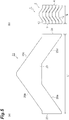
- the prism member 2 has an entrance surface 3 for receiving a terahertz wave, and an exit surface 4 for emitting the terahertz wave received by the entrance surface 3, and a holding surface 7.
- the entrance surface 3 is a surface on which a terahertz wave T is entered into the prism member, and is disposed on one edge side of the prism member 2.
- the terahertz wave T is to be substantially perpendicularly incident on the entrance surface 3.
- the exit surface 4 is a surface from which the terahertz wave T is emitted, and is disposed on another edge side of the prism member 2.
- the terahertz wave T is to be emitted substantially perpendicularly from the exit surface 4 such that the incident axis of the terahertz wave T incident on the entrance surface 3 substantially coincides with the emission axis of the terahertz wave T emitting from the exit surface 4.
- the holding surface 7 is a surface for the wave plate 1 to be held in a holding member such as a holder.
- the holding surfaces 7 are constituted by a total of six surfaces, that is, a first holding surface 7a, a second holding surface 7b, a third holding surface 7c, a fourth holding surface 7d, a fifth holding surface 7e, and a sixth holding surface 7f.
- the prism member 2 is constituted by stacking divided prism members 12 (12a to 12f).
- Fig. 2 (a) is a perspective view illustrating a divided prism member 12 constituting the prism member 2.
- Fig. 2 (b) is a side view of Fig. 2 (a) .
- an optical axis of the terahertz wave T passing through the divided prism members 12 is illustrated in the chained line for descriptive purposes.
- the waveguide region is constituted by, for example, a partial entrance surface 13, a total reflection surface 15, a partial exit surface 14, and an contact surface 16.
- the partial entrance surface 13 is a surface on which a terahertz wave T is entered into the prism member 12, and is disposed on one edge side of the prism member 12. On the partial entrance surface 13, a part of the terahertz wave T is to be substantially perpendicularly incident.
- the total reflection surface 15 is a surface on which a part of the terahertz wave T incident on the partial entrance surface 13 is totally reflected, thereby changing phase of the terahertz wave T.
- the total reflection surfaces 15 are constituted by a total of four surfaces, that is, a first total reflection surface 15a, a second total reflection surface 15b, a third total reflection surface 15c, and a fourth total reflection surface 15d.
- the first total reflection surface 15a is disposed on the partial entrance surface 13 side and is located at the bottom surface of the divided prism member 12; and the second total reflection surface 15b is disposed on the partial entrance surface 13 side and is located at the top surface of the divided prism member 12 so as to be opposite to the first total reflection surface 15a.
- the third total reflection surface 15c is disposed on the partial exit surface 14 side and is located at the top surface of the divided prism member 12; and the fourth total reflection surface 15d is disposed on the partial exit surface 14 side and is located at the bottom surface of the divided prism member 12 so as to be opposite to the third total reflection surface 15c.
- the inclination angles ⁇ 1 to ⁇ 4 between the optical axis of a part of the terahertz wave T and the respective normal directions of the first total reflection surface 15a to the fourth total reflection surface 15d are all, for example, 55° respectively.
- a part of the terahertz wave T incident on the partial entrance surface 13 is totally reflected in order from the first total reflection surface 15a, the second total reflection surface 15b, the third total reflection surface 15c, to the fourth total reflection surface 15d, and then is guided to the partial exit surface 14, as illustrated in Fig. 2 (b) .
- the partial exit surface 14 is a surface from which a part of the terahertz wave T which was totally reflected by the total reflection surfaces 15a to 15d is emitted, and is disposed on another edge side of the divided prism members 12.
- the part of the terahertz wave T is to be emitted substantially perpendicularly from the partial exit surface 14 such that the incident axis of the part of the terahertz wave T incident on the partial entrance surface 13 substantially coincides with the emission axis of the part of the terahertz wave T emitting from the partial exit surface 14.
- An contact surface 16 is a surface which is in contact with the adjacent divided prism members in the stacking direction when constituting the prism member 2 by stacking the divided prism members 12.
- the contact surfaces 16 are constituted by a total of six surfaces, that is, a first contact surface 16a, a second contact surface 16b, a third contact surface 16c, a fourth contact surface 16d, a fifth contact surface 16e, and a sixth contact surface 16f.
- the first contact surface 16a is disposed between the partial entrance surface 13 and the first total reflection surface 15a and is located at the bottom surface of the divided prism member 12; and the second contact surface 16b is disposed between the partial entrance surface 13 and the second total reflection surface 15b and is located at the top surface of the divided prism member 12 so as to be opposite to the first contact surface 16a.
- the third contact surface 16c is disposed between the first total reflection surface 15a and the fourth total reflection surface 15d and is located at the bottom surface of the divided prism member 12; and the fourth contact surface 16d is disposed between the second total reflection surface 15b and the third total reflection surface 15c and is located at the top surface of the divided prism member 12 so as to be opposite to the third contact surface 16c.
- the fifth contact surface 16e is disposed between the fourth total reflection surface 15d and the partial exit surface 14 and is located at the bottom surface of the divided prism member 12; and the sixth contact surface 16f is disposed between the third total reflection surface 15c and the partial exit surface 14 and is located at the top surface of the divided prism member 12 so as to be opposite to the fifth contact surface 16e.
- the first contact surface 16a to the sixth contact surface 16f are all provided flatly and substantially in parallel to the incident axis and the emission axis of the terahertz wave T.
- n represents a ratio (N out /N) between a refractive index N of the divided prism members 12 and a refractive index N out of the medium outside the divided prism members 12, and ⁇ represents an inclination angle between the optical axis of the terahertz wave and the normal direction of the total reflection surface.
- the amount of change in phase ⁇ of the terahertz wave T by the total reflection is independent of the wavelength of the terahertz wave T, but is dependent on the inclination angle ⁇ of the total reflection surface 15. Therefore, a total of the amount of change in phase of the terahertz wave T by the total reflection on each of the total reflection surfaces 15a, 15b, 15c, 15d can achieve a desirable value, by suitably setting the inclination angle ⁇ of each of the total reflection surfaces 15a, 15b, 15c, 15d.
- a desirable amount of change in phase can be realized in every wavelength region even the terahertz wave T has a wide wavelength region. Additionally, in the divided prism members 12, since only the total reflection is utilized without using reflection by a metal and the like, a loss in the terahertz wave T can be suppressed.
- Fig. 3 is a side view of the wave plate 1 illustrated in Fig. 1 .
- the prism member 2 is constituted by stacking so that the contact surfaces 16 of the divided prism members 12, in which six divided prism members 12a to 12f are adjacent thereto, are to be in abutting contact with one another.
- the entrance surface 3 of the prism member 2 is successively constituted by the partial entrance surfaces 13a to 13f of the respective divided prism members 12; and the exit surface 4 is successively constituted by the partial exit surfaces 14a to 14f of the respective divided prism members 12.
- the total reflection surfaces 15 are constituted by a total of twenty-four surfaces, that is, the total reflection surfaces 15a to 15d of the respective divided prism members 12a to 12f.
- a first holding surface 7a, a third holding surface 7c, and a sixth holding surface 7f of the prism member 2 are constituted by the first contact surface 16a, the third contact surface 16c, and the sixth contact surface 16f of the divided prism member 12f arranged at the lowest part, respectively.
- a second holding surface 7b, a fourth holding surface 7d, and a fifth holding surface 7e of the prism member 2 are constituted by the second contact surface 16b, the fourth contact surface 16d, and the fifth contact surface 16e of the divided prism member 12a arranged at the top part, respectively.
- parts T1 to T6 of the terahertz wave T incident on the entrance surface 3 are respectively incident on the partial entrance surfaces 13 of the respective divided prism members 12a to 12f, and are totally reflected in order from the first total reflection surface 15a to the fourth total reflection surface 15d of the respective divided prism members 12a to 12f, and then the parts T1 to T6 of the terahertz wave T get together at the partial exit surfaces 14 of the respective divided prism members 12a to 12f to emit from the exit surface 4.
- Fig. 4 is a partially enlarged view of Fig. 3 .
- a gap portion G is formed between the second total reflection surface 15b of one divided prism member 12 and the first total reflection surface 15a of the adjacent divided prism member 12.
- a space of the gap portion G (distance between the total reflection surface 15a and the total reflection surface 15b) is, for example, at least the same or more of the leaking depth d p of an evanescent wave at the total reflection surfaces 15a, 15b of the terahertz wave.
- the space of the gap portion G is preferably twice or more of the leaking depth d p , more preferably three times or more of the leaking depth d p , and still more preferably six times or more of the leaking depth d p .
- n represents a ratio (N G /N) between a refractive index N of the divided prism members 12 and a refractive index N G of the medium constituting the gap portion G
- ⁇ represents an inclination angle between the optical axis of the terahertz wave and the normal direction of the total reflection surface 15.
- the gap portion G is also formed between the fourth total reflection surface 15d of one divided prism member 12 and the third total reflection surface 15c of the adjacent divided prism member 12.
- the third contact surface 16c of the divided prism member 12 is disposed above the second contact surface 16b and the fifth contact surface 16e (on the fourth contact surface 16d side).
- the prism member 2 is constituted by stacking the divided prism members 12a to 12f. And, the partial entrance surfaces 13a to 13f of the divided prism members 12a to 12f combine to constitute the entrance surface 3 of the prism member 2, and the partial exit surfaces 14a to 14f of the divided prism members 12a to 12f combine to constitute the exit surface 4 of the prism member 2. Therefore, the entrance surface can be enlarged in accordance with the beam diameter of the terahertz wave T, while keeping the size of each of the waveguide regions in the traveling direction of the terahertz wave T suppressed from increasing. Therefore, downsizing of the wave plate can be achieved even with respect to a large beam diameter.
- a case of constituting a 1/2 wave plate 21 with a prism member having an entrance surface 23 with the same size as the entrance surface 3, and being provided with only a single waveguide region, is considered.
- the wave plate 21 in the comparative example illustrated in Fig. 5 (a) includes a prism member 22 having the entrance surface 23, an exit surface 24, a first total reflection surface 25a, a second total reflection surface 25b, a third total reflection surface 25c, and a fourth total reflection surface 25d.
- this wave plate 21 when making the entrance surface 23 and the exit surface 24 responsive to the terahertz wave T having a diameter of 30 mm, the length L' of the prism member 22 in the traveling direction of the terahertz wave T becomes, for example, 122 mm.
- the length L of the divided prism members 12 in the traveling direction of the terahertz wave T becomes, for example, 29 mm.
- the size of the prism member 2 in the traveling direction of the terahertz wave T can be maintained as the size of the divided prism members 12 even when stacking the divided prism members 12, and making the entrance surface 3 and the exit surface 4 responsive to the terahertz wave T having a diameter of 30 mm. Therefore, downsizing of the wave plate 1 can be achieved even with respect to a large beam diameter.
- each of the divided prism members 12a to 12f can realize a desirable amount of change in phase over the whole wavelength region even the terahertz wave T has a wide wavelength region. Therefore, similarly, also the wave plate 1 can realize a desirable amount of change in phase over the whole wavelength region even the terahertz wave T has a wide wavelength region.
- the gap portion G with a space larger than the leaking depth of the evanescent wave on the total reflection surface 15 of the terahertz wave T is arranged between the total reflection surfaces 15 of the adjacent divided prism members 12. Therefore, the evanescent waves on the total reflection surfaces 15 of the terahertz wave T passing through the adjacent divided prism members 12 can be prevented from interfering with each other. Therefore, the amount of change in phase of the terahertz wave T can be a desirable value without being affected by the mutual interference between the evanescent waves.
- the third contact surface 16c of the divided prism member 12 is disposed above the second contact surface 16b and the fifth contact surface 16e (on the fourth contact surface 16d side). Due to such a structure, the terahertz wave T incident around a boundary surface between the divided prism members 12, 12 can be guided onto the total reflection surface 15 without having a loss. Accordingly, occurrence of a loss of light by the wave plate 1 can be reduced.
- the divided prism members 12a to 12f are constituted so that a part of the incident axis and a part of the emission axis of the terahertz wave T substantially match. Therefore, as illustrated in Fig. 3 , when the divided prism members 12a to 12f are stacked, the incident axis and the emission axis of the terahertz wave T in the prism member 2 can be made substantially matched.
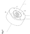
- the wave plate 1 held in a holder 6a can be mounted in a rotating holder 6b, as illustrated in Fig. 7 .
- the wave plate 1 since the incident axis and the emission axis of the terahertz wave T in the prism member 2 substantially coincide, by rotating the rotating holder 6b around the incident axis and the emission axis, the optical system can be easily adjusted without generating deviation in the incident axis and the emission axis of the terahertz wave T.
- the wave plate 1 is provided with the prism member 2 having the holding surfaces 7 which are flat surfaces parallel to the incident axis and the emission axis of the terahertz wave T. Therefore, as illustrated in Fig. 6 , the wave plate 1 can be easily held in the holder 6a by the flat holding surfaces 7.
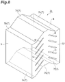
- Fig. 8 is a perspective view illustrating a wave plate in accordance with a modified example.
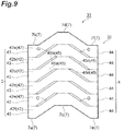
- Fig. 9 is a side view of the wave plate of Fig. 8 .
- a wave plate 31 in accordance with the modified example is different from that of the first embodiment in the point that the wave plate 31 is constituted by a prism member 32 which is integrally formed without using the divided prism members 12.
- waveguide regions 42 (42a to 42f) having partial entrance surfaces 43, partial exit surfaces 44, and total reflection surfaces 45 (45a to 45d), which are similar to the divided prism members 12, are stacked and arranged in the prism member 32; and due to the stacking of each of the waveguide regions 42, each of the partial entrance surfaces 43 successively constitutes the entrance surface 3 of the prism member 32; and each of the partial exit surfaces 44 successively constitutes the exit surface 4 of the prism member 32.
- the prism member 32 may be formed by cutting out from a bulk type material, or may be formed by stacking and fusing the divided prism members 12.
Landscapes
- Physics & Mathematics (AREA)
- General Physics & Mathematics (AREA)
- Optics & Photonics (AREA)
- Optical Modulation, Optical Deflection, Nonlinear Optics, Optical Demodulation, Optical Logic Elements (AREA)
- Investigating Or Analysing Materials By Optical Means (AREA)
- Optical Elements Other Than Lenses (AREA)
- Polarising Elements (AREA)
Claims (1)
- Organe de prisme divisé (12) constituant un organe de prisme (2) ayant une surface d'entrée (3) pour recevoir une onde térahertz (T), et une surface de sortie (4) pour émettre l'onde térahertz (T) depuis la surface d'entrée (3), comprenant :une région de guide d'ondes ayant une surface d'entrée partielle (13) pour recevoir une partie de l'onde térahertz (T), une pluralité de surfaces de réflexion totale pour réfléchir totalement l'onde térahertz entrée depuis la surface d'entrée partielle (13), et une surface de sortie partielle (14) pour émettre l'onde térahertz (T) totalement réfléchie sur les surfaces de réflexion totale (15) ;dans lequel la pluralité de surfaces de réflexion totale comprend une première surface de réflexion totale (15a), une deuxième surface de réflexion totale (15b), une troisième surface de réflexion totale (15c) et une quatrième surface de réflexion totale (15d),où l'organe de prisme divisé (12) est pourvu d'une surface de contact (16) sensiblement parallèle à l'axe incident et à l'axe d'émission de l'onde térahertz (T), où la surface de contact est destinée à entrer en contact avec des organes de prisme divisé (12) adjacents dans la direction d'empilement.
Applications Claiming Priority (3)
| Application Number | Priority Date | Filing Date | Title |
|---|---|---|---|
| JP2013158037A JP6391921B2 (ja) | 2013-07-30 | 2013-07-30 | 波長板及び分割プリズム部材 |
| EP14831381.0A EP3029495B1 (fr) | 2013-07-30 | 2014-05-20 | Lame de phase et élément de prisme divisé |
| PCT/JP2014/063383 WO2015015871A1 (fr) | 2013-07-30 | 2014-05-20 | Lame de phase et élément de prisme divisé |
Related Parent Applications (2)
| Application Number | Title | Priority Date | Filing Date |
|---|---|---|---|
| EP14831381.0A Division-Into EP3029495B1 (fr) | 2013-07-30 | 2014-05-20 | Lame de phase et élément de prisme divisé |
| EP14831381.0A Division EP3029495B1 (fr) | 2013-07-30 | 2014-05-20 | Lame de phase et élément de prisme divisé |
Publications (2)
| Publication Number | Publication Date |
|---|---|
| EP3570082A1 EP3570082A1 (fr) | 2019-11-20 |
| EP3570082B1 true EP3570082B1 (fr) | 2021-07-14 |
Family
ID=52431417
Family Applications (2)
| Application Number | Title | Priority Date | Filing Date |
|---|---|---|---|
| EP19185566.7A Active EP3570082B1 (fr) | 2013-07-30 | 2014-05-20 | Plaque d'ondes et élément à prisme divisé |
| EP14831381.0A Active EP3029495B1 (fr) | 2013-07-30 | 2014-05-20 | Lame de phase et élément de prisme divisé |
Family Applications After (1)
| Application Number | Title | Priority Date | Filing Date |
|---|---|---|---|
| EP14831381.0A Active EP3029495B1 (fr) | 2013-07-30 | 2014-05-20 | Lame de phase et élément de prisme divisé |
Country Status (4)
| Country | Link |
|---|---|
| US (2) | US10591669B2 (fr) |
| EP (2) | EP3570082B1 (fr) |
| JP (1) | JP6391921B2 (fr) |
| WO (1) | WO2015015871A1 (fr) |
Families Citing this family (3)
| Publication number | Priority date | Publication date | Assignee | Title |
|---|---|---|---|---|
| US12494339B2 (en) | 2021-08-25 | 2025-12-09 | Kla Corporation | High resolution, multi-electron beam apparatus |
| US11906770B2 (en) * | 2021-10-21 | 2024-02-20 | KLA Corporal | Monolithic optical retarder |
| KR102893220B1 (ko) * | 2023-10-10 | 2025-11-28 | 국립한국해양대학교산학협력단 | 얇은 금속 시트를 이용한 선택적 시료 측정용 테라헤르츠 경사진 평행 도파로 |
Family Cites Families (19)
| Publication number | Priority date | Publication date | Assignee | Title |
|---|---|---|---|---|
| US4690490A (en) * | 1983-09-27 | 1987-09-01 | Kei Mori | Light diverting device |
| US4975712A (en) * | 1989-01-23 | 1990-12-04 | Trw Inc. | Two-dimensional scanning antenna |
| JPH05347450A (ja) * | 1992-06-12 | 1993-12-27 | Mitsubishi Electric Corp | 波長可変レーザー装置 |
| US5818395A (en) | 1997-01-16 | 1998-10-06 | Trw Inc. | Ultralight collapsible and deployable waveguide lens antenna system |
| EP0889335B1 (fr) * | 1997-06-30 | 2009-06-03 | Hamamatsu Photonics K. K. | Faisceau de fibres optiques et appareil laser à fibre optique utilisant le faisceau de fibres |
| JP2000241767A (ja) * | 1999-02-17 | 2000-09-08 | Canon Inc | 照明装置及びそれを用いた投射装置 |
| JP3817970B2 (ja) * | 1999-05-31 | 2006-09-06 | ウシオ電機株式会社 | 偏光ビームスプリッタおよびそれを用いた液晶表示素子の配向膜光配向用偏光光照射装置 |
| US6356679B1 (en) * | 2000-03-30 | 2002-03-12 | K2 Optronics, Inc. | Optical routing element for use in fiber optic systems |
| DE10021725A1 (de) * | 2000-05-04 | 2001-11-15 | Osram Opto Semiconductors Gmbh | Facettierter Reflektor |
| US6519382B1 (en) * | 2000-09-11 | 2003-02-11 | Optical Switch Corporation | Frustrated total internal reflection switch using waveguides and method of operation |
| JP2002182158A (ja) * | 2000-12-12 | 2002-06-26 | Ushio Inc | 偏光ビームスプリッタを備えた光配向用偏光光照射装置 |
| JP2002189301A (ja) * | 2000-12-22 | 2002-07-05 | Ushio Inc | 光配向用偏光光照射装置 |
| US6463192B1 (en) * | 2001-02-26 | 2002-10-08 | K2 Optronics, Inc. | Non-blocking micro-optic switch matrix for use in fiber optic systems |
| JP4645173B2 (ja) * | 2004-11-26 | 2011-03-09 | 株式会社ニコン | 分光器、及びこれを備えている顕微分光装置 |
| EP2273254A4 (fr) | 2008-04-30 | 2014-02-26 | Hamamatsu Photonics Kk | Dispositif de mesure d'ondes térahertziennes de réflexion totale |
| JP2009300108A (ja) * | 2008-06-10 | 2009-12-24 | Sony Corp | テラヘルツ分光装置 |
| JP5071294B2 (ja) * | 2008-07-29 | 2012-11-14 | 株式会社ニコン | チューナブルフィルタ、光源装置およびスペクトル分布測定装置 |
| EP2843460A1 (fr) * | 2008-10-31 | 2015-03-04 | Hewlett-Packard Development Company, L.P. | Coupleurs et diviseurs de faisceau optique |
| JP5894575B2 (ja) * | 2011-03-29 | 2016-03-30 | 浜松ホトニクス株式会社 | テラヘルツ波分光計測装置 |
-
2013
- 2013-07-30 JP JP2013158037A patent/JP6391921B2/ja active Active
-
2014
- 2014-05-20 US US14/906,924 patent/US10591669B2/en active Active
- 2014-05-20 EP EP19185566.7A patent/EP3570082B1/fr active Active
- 2014-05-20 WO PCT/JP2014/063383 patent/WO2015015871A1/fr not_active Ceased
- 2014-05-20 EP EP14831381.0A patent/EP3029495B1/fr active Active
-
2020
- 2020-01-10 US US16/739,214 patent/US10908355B2/en active Active
Also Published As
| Publication number | Publication date |
|---|---|
| US20200150339A1 (en) | 2020-05-14 |
| US10591669B2 (en) | 2020-03-17 |
| WO2015015871A1 (fr) | 2015-02-05 |
| US20160154176A1 (en) | 2016-06-02 |
| EP3029495A4 (fr) | 2017-03-01 |
| US10908355B2 (en) | 2021-02-02 |
| EP3029495B1 (fr) | 2021-10-13 |
| EP3570082A1 (fr) | 2019-11-20 |
| JP6391921B2 (ja) | 2018-09-19 |
| EP3029495A1 (fr) | 2016-06-08 |
| JP2015028559A (ja) | 2015-02-12 |
Similar Documents
| Publication | Publication Date | Title |
|---|---|---|
| US11454809B2 (en) | Display waveguide assembly with color cross-coupling | |
| JP6287095B2 (ja) | 光学デバイス及び電子機器 | |
| US20200116996A1 (en) | Display waveguide assembly with color cross-coupling | |
| US10908355B2 (en) | Wave plate and divided prism member | |
| US9971159B2 (en) | Reflective laser line-beam generator | |
| US20160025567A1 (en) | Angle limiting reflector and optical dispersive device including the same | |
| JP2017129744A (ja) | 光合波装置 | |
| EP3355422B1 (fr) | Laser à cascade quantique à cavité externe accordable en longueur d'onde utilisant un réseau d'immersion à angle réglé en tant qu'élément de filtre de sélection de longueur d'onde | |
| US20090002834A1 (en) | Device for Homogenizing Light | |
| US9915786B2 (en) | Transmissive photonic crystal fiber ring resonator employing single optical beam-splitter | |
| CN104678558A (zh) | 光分路装置 | |
| EP3176552A1 (fr) | Dispositif et procede d'evaluation de collimation | |
| EP3836321A1 (fr) | Dispositif laser à semi-conducteur de type résonateur externe | |
| EP3321650A1 (fr) | Interféromètre optique | |
| CN110036543A (zh) | 激光振荡装置 | |
| WO2015008648A1 (fr) | Lame de phase | |
| US9599875B2 (en) | Five-wave optical parametric oscillator with V-ring geometry | |
| JP4839845B2 (ja) | 分光装置 | |
| US7130045B2 (en) | Monochromator and method of use | |
| JP5742331B2 (ja) | レーザ光スキャナ | |
| JP6358710B2 (ja) | 回折光学素子 | |
| US9551866B1 (en) | Optical scanning system and scanning lens | |
| JP7041903B2 (ja) | 光合波装置 | |
| US20230017729A1 (en) | Compact etalon structure | |
| CN103941414A (zh) | 基于异构二维光子晶体的y型偏振滤波分束器 |
Legal Events
| Date | Code | Title | Description |
|---|---|---|---|
| PUAI | Public reference made under article 153(3) epc to a published international application that has entered the european phase |
Free format text: ORIGINAL CODE: 0009012 |
|
| STAA | Information on the status of an ep patent application or granted ep patent |
Free format text: STATUS: REQUEST FOR EXAMINATION WAS MADE |
|
| 17P | Request for examination filed |
Effective date: 20190710 |
|
| AC | Divisional application: reference to earlier application |
Ref document number: 3029495 Country of ref document: EP Kind code of ref document: P |
|
| AK | Designated contracting states |
Kind code of ref document: A1 Designated state(s): AL AT BE BG CH CY CZ DE DK EE ES FI FR GB GR HR HU IE IS IT LI LT LU LV MC MK MT NL NO PL PT RO RS SE SI SK SM TR |
|
| GRAP | Despatch of communication of intention to grant a patent |
Free format text: ORIGINAL CODE: EPIDOSNIGR1 |
|
| STAA | Information on the status of an ep patent application or granted ep patent |
Free format text: STATUS: GRANT OF PATENT IS INTENDED |
|
| INTG | Intention to grant announced |
Effective date: 20210210 |
|
| RIN1 | Information on inventor provided before grant (corrected) |
Inventor name: YASUDA, TAKASHI Inventor name: NAKANISHI, ATSUSHI Inventor name: KAWADA, YOICHI |
|
| GRAS | Grant fee paid |
Free format text: ORIGINAL CODE: EPIDOSNIGR3 |
|
| GRAA | (expected) grant |
Free format text: ORIGINAL CODE: 0009210 |
|
| STAA | Information on the status of an ep patent application or granted ep patent |
Free format text: STATUS: THE PATENT HAS BEEN GRANTED |
|
| AC | Divisional application: reference to earlier application |
Ref document number: 3029495 Country of ref document: EP Kind code of ref document: P |
|
| AK | Designated contracting states |
Kind code of ref document: B1 Designated state(s): AL AT BE BG CH CY CZ DE DK EE ES FI FR GB GR HR HU IE IS IT LI LT LU LV MC MK MT NL NO PL PT RO RS SE SI SK SM TR |
|
| REG | Reference to a national code |
Ref country code: GB Ref legal event code: FG4D |
|
| REG | Reference to a national code |
Ref country code: DE Ref legal event code: R096 Ref document number: 602014078849 Country of ref document: DE |
|
| REG | Reference to a national code |
Ref country code: IE Ref legal event code: FG4D |
|
| REG | Reference to a national code |
Ref country code: AT Ref legal event code: REF Ref document number: 1411109 Country of ref document: AT Kind code of ref document: T Effective date: 20210815 |
|
| REG | Reference to a national code |
Ref country code: LT Ref legal event code: MG9D |
|
| REG | Reference to a national code |
Ref country code: NL Ref legal event code: MP Effective date: 20210714 |
|
| REG | Reference to a national code |
Ref country code: AT Ref legal event code: MK05 Ref document number: 1411109 Country of ref document: AT Kind code of ref document: T Effective date: 20210714 |
|
| PG25 | Lapsed in a contracting state [announced via postgrant information from national office to epo] |
Ref country code: RS Free format text: LAPSE BECAUSE OF FAILURE TO SUBMIT A TRANSLATION OF THE DESCRIPTION OR TO PAY THE FEE WITHIN THE PRESCRIBED TIME-LIMIT Effective date: 20210714 Ref country code: SE Free format text: LAPSE BECAUSE OF FAILURE TO SUBMIT A TRANSLATION OF THE DESCRIPTION OR TO PAY THE FEE WITHIN THE PRESCRIBED TIME-LIMIT Effective date: 20210714 Ref country code: ES Free format text: LAPSE BECAUSE OF FAILURE TO SUBMIT A TRANSLATION OF THE DESCRIPTION OR TO PAY THE FEE WITHIN THE PRESCRIBED TIME-LIMIT Effective date: 20210714 Ref country code: FI Free format text: LAPSE BECAUSE OF FAILURE TO SUBMIT A TRANSLATION OF THE DESCRIPTION OR TO PAY THE FEE WITHIN THE PRESCRIBED TIME-LIMIT Effective date: 20210714 Ref country code: HR Free format text: LAPSE BECAUSE OF FAILURE TO SUBMIT A TRANSLATION OF THE DESCRIPTION OR TO PAY THE FEE WITHIN THE PRESCRIBED TIME-LIMIT Effective date: 20210714 Ref country code: NL Free format text: LAPSE BECAUSE OF FAILURE TO SUBMIT A TRANSLATION OF THE DESCRIPTION OR TO PAY THE FEE WITHIN THE PRESCRIBED TIME-LIMIT Effective date: 20210714 Ref country code: NO Free format text: LAPSE BECAUSE OF FAILURE TO SUBMIT A TRANSLATION OF THE DESCRIPTION OR TO PAY THE FEE WITHIN THE PRESCRIBED TIME-LIMIT Effective date: 20211014 Ref country code: PT Free format text: LAPSE BECAUSE OF FAILURE TO SUBMIT A TRANSLATION OF THE DESCRIPTION OR TO PAY THE FEE WITHIN THE PRESCRIBED TIME-LIMIT Effective date: 20211115 Ref country code: LT Free format text: LAPSE BECAUSE OF FAILURE TO SUBMIT A TRANSLATION OF THE DESCRIPTION OR TO PAY THE FEE WITHIN THE PRESCRIBED TIME-LIMIT Effective date: 20210714 Ref country code: BG Free format text: LAPSE BECAUSE OF FAILURE TO SUBMIT A TRANSLATION OF THE DESCRIPTION OR TO PAY THE FEE WITHIN THE PRESCRIBED TIME-LIMIT Effective date: 20211014 Ref country code: AT Free format text: LAPSE BECAUSE OF FAILURE TO SUBMIT A TRANSLATION OF THE DESCRIPTION OR TO PAY THE FEE WITHIN THE PRESCRIBED TIME-LIMIT Effective date: 20210714 |
|
| PG25 | Lapsed in a contracting state [announced via postgrant information from national office to epo] |
Ref country code: PL Free format text: LAPSE BECAUSE OF FAILURE TO SUBMIT A TRANSLATION OF THE DESCRIPTION OR TO PAY THE FEE WITHIN THE PRESCRIBED TIME-LIMIT Effective date: 20210714 Ref country code: LV Free format text: LAPSE BECAUSE OF FAILURE TO SUBMIT A TRANSLATION OF THE DESCRIPTION OR TO PAY THE FEE WITHIN THE PRESCRIBED TIME-LIMIT Effective date: 20210714 Ref country code: GR Free format text: LAPSE BECAUSE OF FAILURE TO SUBMIT A TRANSLATION OF THE DESCRIPTION OR TO PAY THE FEE WITHIN THE PRESCRIBED TIME-LIMIT Effective date: 20211015 |
|
| REG | Reference to a national code |
Ref country code: DE Ref legal event code: R097 Ref document number: 602014078849 Country of ref document: DE |
|
| PG25 | Lapsed in a contracting state [announced via postgrant information from national office to epo] |
Ref country code: DK Free format text: LAPSE BECAUSE OF FAILURE TO SUBMIT A TRANSLATION OF THE DESCRIPTION OR TO PAY THE FEE WITHIN THE PRESCRIBED TIME-LIMIT Effective date: 20210714 |
|
| PLBE | No opposition filed within time limit |
Free format text: ORIGINAL CODE: 0009261 |
|
| STAA | Information on the status of an ep patent application or granted ep patent |
Free format text: STATUS: NO OPPOSITION FILED WITHIN TIME LIMIT |
|
| PG25 | Lapsed in a contracting state [announced via postgrant information from national office to epo] |
Ref country code: SM Free format text: LAPSE BECAUSE OF FAILURE TO SUBMIT A TRANSLATION OF THE DESCRIPTION OR TO PAY THE FEE WITHIN THE PRESCRIBED TIME-LIMIT Effective date: 20210714 Ref country code: SK Free format text: LAPSE BECAUSE OF FAILURE TO SUBMIT A TRANSLATION OF THE DESCRIPTION OR TO PAY THE FEE WITHIN THE PRESCRIBED TIME-LIMIT Effective date: 20210714 Ref country code: RO Free format text: LAPSE BECAUSE OF FAILURE TO SUBMIT A TRANSLATION OF THE DESCRIPTION OR TO PAY THE FEE WITHIN THE PRESCRIBED TIME-LIMIT Effective date: 20210714 Ref country code: EE Free format text: LAPSE BECAUSE OF FAILURE TO SUBMIT A TRANSLATION OF THE DESCRIPTION OR TO PAY THE FEE WITHIN THE PRESCRIBED TIME-LIMIT Effective date: 20210714 Ref country code: CZ Free format text: LAPSE BECAUSE OF FAILURE TO SUBMIT A TRANSLATION OF THE DESCRIPTION OR TO PAY THE FEE WITHIN THE PRESCRIBED TIME-LIMIT Effective date: 20210714 Ref country code: AL Free format text: LAPSE BECAUSE OF FAILURE TO SUBMIT A TRANSLATION OF THE DESCRIPTION OR TO PAY THE FEE WITHIN THE PRESCRIBED TIME-LIMIT Effective date: 20210714 |
|
| 26N | No opposition filed |
Effective date: 20220419 |
|
| PG25 | Lapsed in a contracting state [announced via postgrant information from national office to epo] |
Ref country code: IT Free format text: LAPSE BECAUSE OF FAILURE TO SUBMIT A TRANSLATION OF THE DESCRIPTION OR TO PAY THE FEE WITHIN THE PRESCRIBED TIME-LIMIT Effective date: 20210714 |
|
| REG | Reference to a national code |
Ref country code: CH Ref legal event code: PL |
|
| REG | Reference to a national code |
Ref country code: BE Ref legal event code: MM Effective date: 20220531 |
|
| PG25 | Lapsed in a contracting state [announced via postgrant information from national office to epo] |
Ref country code: MC Free format text: LAPSE BECAUSE OF FAILURE TO SUBMIT A TRANSLATION OF THE DESCRIPTION OR TO PAY THE FEE WITHIN THE PRESCRIBED TIME-LIMIT Effective date: 20210714 Ref country code: LU Free format text: LAPSE BECAUSE OF NON-PAYMENT OF DUE FEES Effective date: 20220520 Ref country code: LI Free format text: LAPSE BECAUSE OF NON-PAYMENT OF DUE FEES Effective date: 20220531 Ref country code: CH Free format text: LAPSE BECAUSE OF NON-PAYMENT OF DUE FEES Effective date: 20220531 |
|
| PG25 | Lapsed in a contracting state [announced via postgrant information from national office to epo] |
Ref country code: IE Free format text: LAPSE BECAUSE OF NON-PAYMENT OF DUE FEES Effective date: 20220520 |
|
| PG25 | Lapsed in a contracting state [announced via postgrant information from national office to epo] |
Ref country code: BE Free format text: LAPSE BECAUSE OF NON-PAYMENT OF DUE FEES Effective date: 20220531 |
|
| P01 | Opt-out of the competence of the unified patent court (upc) registered |
Effective date: 20230509 |
|
| PG25 | Lapsed in a contracting state [announced via postgrant information from national office to epo] |
Ref country code: HU Free format text: LAPSE BECAUSE OF FAILURE TO SUBMIT A TRANSLATION OF THE DESCRIPTION OR TO PAY THE FEE WITHIN THE PRESCRIBED TIME-LIMIT; INVALID AB INITIO Effective date: 20140520 |
|
| PG25 | Lapsed in a contracting state [announced via postgrant information from national office to epo] |
Ref country code: MK Free format text: LAPSE BECAUSE OF FAILURE TO SUBMIT A TRANSLATION OF THE DESCRIPTION OR TO PAY THE FEE WITHIN THE PRESCRIBED TIME-LIMIT Effective date: 20210714 Ref country code: CY Free format text: LAPSE BECAUSE OF FAILURE TO SUBMIT A TRANSLATION OF THE DESCRIPTION OR TO PAY THE FEE WITHIN THE PRESCRIBED TIME-LIMIT Effective date: 20210714 |
|
| PG25 | Lapsed in a contracting state [announced via postgrant information from national office to epo] |
Ref country code: TR Free format text: LAPSE BECAUSE OF FAILURE TO SUBMIT A TRANSLATION OF THE DESCRIPTION OR TO PAY THE FEE WITHIN THE PRESCRIBED TIME-LIMIT Effective date: 20210714 |
|
| PG25 | Lapsed in a contracting state [announced via postgrant information from national office to epo] |
Ref country code: MT Free format text: LAPSE BECAUSE OF FAILURE TO SUBMIT A TRANSLATION OF THE DESCRIPTION OR TO PAY THE FEE WITHIN THE PRESCRIBED TIME-LIMIT Effective date: 20210714 |
|
| PGFP | Annual fee paid to national office [announced via postgrant information from national office to epo] |
Ref country code: GB Payment date: 20250327 Year of fee payment: 12 |
|
| PGFP | Annual fee paid to national office [announced via postgrant information from national office to epo] |
Ref country code: DE Payment date: 20250402 Year of fee payment: 12 |
|
| PGFP | Annual fee paid to national office [announced via postgrant information from national office to epo] |
Ref country code: FR Payment date: 20250401 Year of fee payment: 12 |