EP3571760B1 - Elektronische vorrichtung, insbesondere ein lichtmaschinenregler, und verfahren zur regelung solch einer vorrichtung - Google Patents
Elektronische vorrichtung, insbesondere ein lichtmaschinenregler, und verfahren zur regelung solch einer vorrichtung Download PDFInfo
- Publication number
- EP3571760B1 EP3571760B1 EP18700357.9A EP18700357A EP3571760B1 EP 3571760 B1 EP3571760 B1 EP 3571760B1 EP 18700357 A EP18700357 A EP 18700357A EP 3571760 B1 EP3571760 B1 EP 3571760B1
- Authority
- EP
- European Patent Office
- Prior art keywords
- pair
- transistors
- transistor
- terminal
- inductor
- Prior art date
- Legal status (The legal status is an assumption and is not a legal conclusion. Google has not performed a legal analysis and makes no representation as to the accuracy of the status listed.)
- Active
Links
Images


Classifications
-
- H—ELECTRICITY
- H02—GENERATION; CONVERSION OR DISTRIBUTION OF ELECTRIC POWER
- H02P—CONTROL OR REGULATION OF ELECTRIC MOTORS, ELECTRIC GENERATORS OR DYNAMO-ELECTRIC CONVERTERS; CONTROLLING TRANSFORMERS, REACTORS OR CHOKE COILS
- H02P9/00—Arrangements for controlling electric generators for the purpose of obtaining a desired output
- H02P9/10—Control effected upon generator excitation circuit to reduce harmful effects of overloads or transients, e.g. sudden application of load, sudden removal of load, sudden change of load
- H02P9/12—Control effected upon generator excitation circuit to reduce harmful effects of overloads or transients, e.g. sudden application of load, sudden removal of load, sudden change of load for demagnetising; for reducing effects of remanence; for preventing pole reversal
-
- H—ELECTRICITY
- H02—GENERATION; CONVERSION OR DISTRIBUTION OF ELECTRIC POWER
- H02K—DYNAMO-ELECTRIC MACHINES
- H02K11/00—Structural association of dynamo-electric machines with electric components or with devices for shielding, monitoring or protection
- H02K11/04—Structural association of dynamo-electric machines with electric components or with devices for shielding, monitoring or protection for rectification
- H02K11/049—Rectifiers associated with stationary parts, e.g. stator cores
- H02K11/05—Rectifiers associated with casings, enclosures or brackets
-
- H—ELECTRICITY
- H02—GENERATION; CONVERSION OR DISTRIBUTION OF ELECTRIC POWER
- H02K—DYNAMO-ELECTRIC MACHINES
- H02K7/00—Arrangements for handling mechanical energy structurally associated with dynamo-electric machines, e.g. structural association with mechanical driving motors or auxiliary dynamo-electric machines
- H02K7/18—Structural association of electric generators with mechanical driving motors, e.g. with turbines
- H02K7/1807—Rotary generators
- H02K7/1815—Rotary generators structurally associated with reciprocating piston engines
-
- H—ELECTRICITY
- H02—GENERATION; CONVERSION OR DISTRIBUTION OF ELECTRIC POWER
- H02P—CONTROL OR REGULATION OF ELECTRIC MOTORS, ELECTRIC GENERATORS OR DYNAMO-ELECTRIC CONVERTERS; CONTROLLING TRANSFORMERS, REACTORS OR CHOKE COILS
- H02P9/00—Arrangements for controlling electric generators for the purpose of obtaining a desired output
- H02P9/14—Arrangements for controlling electric generators for the purpose of obtaining a desired output by variation of field
- H02P9/26—Arrangements for controlling electric generators for the purpose of obtaining a desired output by variation of field using discharge tubes or semiconductor devices
- H02P9/30—Arrangements for controlling electric generators for the purpose of obtaining a desired output by variation of field using discharge tubes or semiconductor devices using semiconductor devices
- H02P9/305—Arrangements for controlling electric generators for the purpose of obtaining a desired output by variation of field using discharge tubes or semiconductor devices using semiconductor devices controlling voltage
-
- H—ELECTRICITY
- H05—ELECTRIC TECHNIQUES NOT OTHERWISE PROVIDED FOR
- H05K—PRINTED CIRCUITS; CASINGS OR CONSTRUCTIONAL DETAILS OF ELECTRIC APPARATUS; MANUFACTURE OF ASSEMBLAGES OF ELECTRICAL COMPONENTS
- H05K7/00—Constructional details common to different types of electric apparatus
- H05K7/14—Mounting supporting structure in casing or on frame or rack
- H05K7/1422—Printed circuit boards receptacles, e.g. stacked structures, electronic circuit modules or box like frames
- H05K7/1427—Housings
- H05K7/1432—Housings specially adapted for power drive units or power converters
- H05K7/14322—Housings specially adapted for power drive units or power converters wherein the control and power circuits of a power converter are arranged within the same casing
-
- H—ELECTRICITY
- H05—ELECTRIC TECHNIQUES NOT OTHERWISE PROVIDED FOR
- H05K—PRINTED CIRCUITS; CASINGS OR CONSTRUCTIONAL DETAILS OF ELECTRIC APPARATUS; MANUFACTURE OF ASSEMBLAGES OF ELECTRICAL COMPONENTS
- H05K7/00—Constructional details common to different types of electric apparatus
- H05K7/20—Modifications to facilitate cooling, ventilating, or heating
- H05K7/2089—Modifications to facilitate cooling, ventilating, or heating for power electronics, e.g. for inverters for controlling motor
- H05K7/209—Heat transfer by conduction from internal heat source to heat radiating structure
-
- H—ELECTRICITY
- H02—GENERATION; CONVERSION OR DISTRIBUTION OF ELECTRIC POWER
- H02P—CONTROL OR REGULATION OF ELECTRIC MOTORS, ELECTRIC GENERATORS OR DYNAMO-ELECTRIC CONVERTERS; CONTROLLING TRANSFORMERS, REACTORS OR CHOKE COILS
- H02P2101/00—Special adaptation of control arrangements for generators
- H02P2101/25—Special adaptation of control arrangements for generators for combustion engines
Definitions
- the present invention relates to electronic devices such as variators or regulators, comprising a power stage.
- Variators or regulators are devices used in conjunction with industrial motors or alternators to control their speed or voltage.
- These devices conventionally include power components, such as IGBTs or MOSFETs for example, mounted on radiators, and fairly large electrochemical capacitors.
- the trend is to seek to reduce their bulk.
- Requirement US 2010/0202109 describes a device in which the capacitors are arranged next to the radiator, and pass through openings of a cooling air guide.
- the patent US 8810178 discloses a speed variator comprising a housing provided with openings through which the capacitors pass. A seal in the form of a perforated sheet is arranged under the openings of the housing. A removable cover covers the ends of the capacitors which protrude from the openings.
- the utility model CN205430848 U describes a variator whose radiator carries, via spacers, a printed circuit board on which the capacitors are soldered.
- the radiator has a cutout into which the capacitors extend.
- Requirement US 2014/077745 describes a device for controlling the drive of a motor comprising at least two inverters and a control device making it possible to switch from a defective inverter to a non-defective inverter.
- Requirement DE 102008037064 describes a switching device connected to two sources of electrical energy.
- Requirement EP 2747270 describes an assembly comprising two transistors in parallel controlled simultaneously to produce an alternating voltage in order to power an inductive load.
- voltage regulators in order to provide an excitation current to wound rotor alternators, voltage regulators conventionally use a power bridge consisting of at least an IGBT and a freewheeling diode.
- a half H-bridge can be used to invert the voltage across the alternator inductor.
- Certain extreme operating conditions can cause one of these power components to break, such as overexcitation or use under excessive ambient temperature. This breakage renders the device completely inoperative and the overexcitation or underexcitation generated can, in certain applications such as the extraction of tunnel fumes, the supply of electricity to a hospital, or the power supply of the cooling pumps of nuclear reactors, prove to be critical.
- the invention aims to meet all or part of these needs.
- the application relates to an electronic device, also called an apparatus, in particular a speed variator or alternator regulator, comprising at least one power component mounted on a heat sink, also called a radiator, and a plurality of capacitors extending to through at least one opening in the heatsink.
- the device comprises a recess in which is received a sheet seal applying on the one hand to an interior face of the heatsink and on the other hand to an interior face facing a housing attached to the heatsink, the interior faces of the heatsink and the housing coming into contact.
- This aspect of the application contributes to the compactness of the device while ensuring efficient cooling of the power component.
- the seal prevents entry of water in the device, and the fact that it is received in a recess makes it possible to provide contact surfaces between the heatsink and the housing to promote thermal transfer from the heatsink to the housing.
- the recess is preferably made in the housing.
- the latter can be made in two assembled parts.
- the housing is for example metallic or plastic.
- At least one of the housing and the heatsink may include centering pins and the joint have corresponding holes in which the centering pins are engaged. This limits the risk of incorrect positioning of the joint in the aforementioned recess.
- the joint may include an opening in which is placed a metal spacer extending between the heatsink and an additional power component, in particular a diode bridge.
- the power component is applied to the heatsink through an opening in the housing.
- we can improve the quality of the thermal contact between the power component and the heatsink.
- the power component can be soldered to a printed circuit board of a power card, this board having slots to form flexible tabs on which extend conductive tracks onto which the pins of the power component are soldered.
- the device can include several, for example five, capacitors arranged in a U, the concavity of the U being oriented towards the power component. This allows for further compactness.
- the power component may include a plurality of power transistors, in particular IGBTs or MOSFETs.
- the application also has for object, according to a second aspect independent of the first but which can advantageously be combined with it, an electronic device, in particular speed variator or alternator regulator, comprising a heat sink and a power card comprising a printed circuit board, housed in a housing.
- an electronic device in particular speed variator or alternator regulator, comprising a heat sink and a power card comprising a printed circuit board, housed in a housing.
- the device comprises a part fixed on the one hand to the heatsink and fixed on the other hand to the plate and coming into contact with at least one conductive track of the card power, so as to ensure electrical contact between the heatsink and said track, this part having a face accessible from the outside of the device for fixing a lug connected to a ground and/or earth cable.
- This assembly makes it possible to establish both the electrical and mechanical connection between the heatsink and the power card, in a reliable manner and contributing to the compactness of the device, since the same part can also be used for an external connection.
- the part may have a hole to receive a screw for fixing said terminal.
- the device may include a housing having an opening for the passage of the part.
- This housing may comprise two assembled parts, the opening being made in a part of the housing in contact with the heatsink.
- the power card can be fixed on the housing, in particular on the screw receiving barrels thereof.
- the device may include a printed circuit board between that of the power card and the heatsink.
- This board may carry connectors and/or terminal blocks. Having such a plate makes it possible to use the space left free under the power card and to further improve the compactness of the device.
- the device preferably includes connectors and/or terminal blocks on three sides as well as on its front face.
- the application also has as its object, according to a third of its aspects, independent of the two aspects above but which can advantageously be combined with any of these, an electronic device, in particular speed variator or alternator regulator , comprising a housing having on the front a housing for receiving an annex module, a hatch for closing this housing, and an electronic circuit comprising an interface card defining a housing for receiving a memory card, opening into the housing reception of the annex module.
- an electronic device in particular speed variator or alternator regulator , comprising a housing having on the front a housing for receiving an annex module, a hatch for closing this housing, and an electronic circuit comprising an interface card defining a housing for receiving a memory card, opening into the housing reception of the annex module.
- the application makes it possible to prohibit access to the memory card as long as the hatch is in place, which is the normal situation, the hatch being only intended to be removed for a maintenance operation.
- the device can thus advantageously include a tamper-evident label covering at least partially the hatch.
- having the memory card reception slot in this location allows you to take advantage of the clearance offered by the annex module reception slot for inserting and removing the card, which contributes to compactness. of the device and its ergonomics.
- the interface card preferably includes a screen and buttons accessible through holes in the housing.
- the memory card slot preferably opens into a recess in the housing intended to receive a locking tab of the hatch.
- This locking tab preferably includes a hole for a screw to pass through.
- the device is configured to record an operating history of the device on the memory card.
- the device has at least one connector on the front, in particular of the RJ45 or USB type.
- This connector can be used to update the device, without having to carry out any disassembly.
- This or these front connectors can be carried by extensions of a printed circuit board of the interface card, extending on either side of the aforementioned recess intended to receive the locking tab of the hatch. This allows for further compactness.
- the housing may comprise assembled lower and upper parts, the housing being made in the upper housing part.
- the lower part is advantageously fixed to a heat sink, the housing housing a power card and a control card superimposed, the interface card being arranged above the control card, the housing extending under the card. interface when the device is placed vertically with the opening of the memory card slot facing downwards.
- Such an arrangement turns out to be ergonomic, compact and easy to assemble and maintain.
- Such an aspect of the invention provides increased reliability in the operation of the device.
- the control circuit is advantageously arranged so that, in the event of failure of a transistor of the first pair causing it to remain in open circuit, send the pulsed control signal to the other transistor of this pair.
- the device comprises a second pair of transistors connected in parallel between a second output to be connected to the load and the opposite terminal of the direct bus, at least one diode connecting the second output to the terminal of the direct bus, at least one of the transistors of the second pair being controlled by the control circuit so as to be conducting during normal operation of the device.
- the other transistor of the second pair is controlled by the control circuit so as to be blocked during normal operation.
- the control circuit is preferably arranged to, in the event of failure of one of the transistors of the second pair causing it to remain in an open circuit, to control the other transistor of this pair to saturate it.
- the control circuit is preferably arranged to, in the event of failure of a transistor of the first pair causing it to remain in short circuit, to control the second transistor of this pair to saturate it, to maintain a transistor of the other pair in the off state and send the pulsed control signal to the other transistor of this second pair.
- the device may include two freewheeling diodes in parallel.
- the device can also include two diodes in parallel connecting the second output to the DC bus terminal.
- the device is advantageously made so as to be able to operate in inversion mode of the voltage across the load, also called "negative forcing", when the current in the load must be quickly canceled for the purposes of regulation, mode in in which the transistors of the first pair are driven off and the two transistors of the second pair also.
- the pulsed control signal is preferably a PWM (Pulse Width Modulation) control signal.
- the transistors of the first pair may belong to a power module comprising three branches in parallel, each branch comprising two transistors in series, and a seventh transistor in series with a diode, the assembly formed by this transistor in series with the diode being connected in parallel with the three branches, the transistors of the first pair each being taken within a respective branch.
- One of the transistors of the second pair can be taken from the remaining branch and the other transistor can be made up of the transistor which is in series with the diode.
- the transistors can be IGBTs or MOSFETs, or can be replaced by thyristors or bipolar transistors.
- the components used to make the bridge are IGBTs.
- the invention also relates to a method of regulating an alternator as defined in independent claim 12.
- the application according to this aspect facilitates the assembly of the device in different configurations of available space, making it possible to choose the most suitable elements.
- the elements of the first and/or second set may each include two tabs.
- the elements of the first set may include at least one hole arranged substantially in the extension of a tongue.
- the elements of the second set can each include at least one hole arranged laterally on the side of the heatsink.
- the elements can each come axially into abutment against a longitudinal end of the dissipator.
- the tabs can be, when the elements are mounted on the heatsink, located in a plane offset from that of the tabs.
- the profile may include slides for receiving the tongues, each formed of two fins provided with returns directed towards each other and an intermediate fin of lower height, provided with a pad on its free edge.
- the tabs may have tapped holes to receive tightening screws of the aforementioned pads, bearing on the latter when tightened.
- the device 1 shown on the figures 1 to 12 is an alternator regulator, but the invention is not limited to an alternator regulator and also applies to a speed variator or an inverter, among other devices using power components and capacitors relatively bulky electrochemicals.
- the device 1 comprises at the rear a heat sink 10, also called a radiator, which has parallel fins 11 connecting at their base to a wall 12.
- the radiator 10 is conventionally made of aluminum or aluminum alloy at the rear. help from a sector for example.
- the device 1 can be without a fan, the cooling of the radiator 10 taking place by natural convection only.
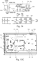
- the radiator 10 defines two longitudinal slides 13 each extending along the outermost fin 11a, intended to receive fixing elements 20 or 20' of different shapes, shown respectively on the figures 2 And 3 .
- the fin 11a has on its free edge an inward return 11b.
- This return 11b faces a return 11c directed towards the fin 11a, carried by a fin 11d of the radiator 10, as can be seen in the Figure 10B .
- Returns 11b and 11c are coplanar.
- An intermediate fin 11g, lower, extends between the fins 11a and 11d. This 11g fin is provided on its free edge with a ribbed 11h pad.
- Elements 20 and 20' are used to attach the device to a receiving surface.
- Each element 20 comprises two tongues 21 each engaged in a slide 13, these tongues 21 being joined by a strip 22 doubly bent so as to define a fixing tab 23 parallel to the strip 22, or perpendicular to the tongues 21, but located at a height different.
- the legs 23 are each crossed by two holes 24.
- the strip 22 is replaced by an angle bracket 25 provided with two fixing lugs 26 directed towards the device 1, whereas in the example of the figure 2 the tabs 23 are directed outwards and not towards the device 1.
- Each tab 26 is provided with a hole 24.
- the user wishing to fix the device 1 chooses the fixing elements 20 or 20' adapted to the specific case, engages them in the slides 23.
- the device 1 comprises several electronic cards including a so-called power card 30 which carries electrochemical DC bus capacitors 31, relatively bulky, for example with a capacity greater than or equal to 200 ⁇ F under an insulation voltage greater than or equal to 250 VDC, notably 400 VDC
- capacitors 31 extend towards the rear in an opening 15 of the radiator 10.
- the capacitors 31 are five in number, and the opening 15 has the general shape of a U, whose concavity is turned inwards, as can be seen on the figures 2 Or 3 notably.
- the height of the fins 11 is sufficient so that the capacitors 31 do not protrude from the radiator 10 towards the rear; thus, the capacitors 31 remain relatively protected from shocks by the fins 11.
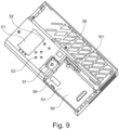
- the device 1 comprises a housing comprising a lower part 40 and an upper part 50, shown on the figures 6 And 9 respectively.
- These parts 40 and 50 are preferably made of plastic, preferably reinforced, but alternatively are made of metal, for example aluminum.
- the lower part 40 is made with an opening 41 for the passage of the capacitors 31.
- a recess 42 is formed on the rear face of this lower part around the opening 41 to accommodate a seal 70 formed from a sheet of elastomeric material provided with holes for the passage of each of the capacitors 31.
- the seal 70 applies both to the periphery of the cylindrical body of each capacitor 31 and to the facing faces of the lower housing part 40 and the radiator 10.
- the lower part of the housing 40 has positioning pins 48 and the joint 70 has corresponding holes 72 (visible on the figure 4 ).
- the seal 70 includes in the example illustrated a window 74 for the passage of a spacer 80 fixed against the radiator 10, the thickness of which is slightly greater than that of the seal 70.
- the lower part 40 of the housing has an opening 49 for placing a power module 90 against the radiator 10.
- This opening 49 communicates with the opening 41, which allows the fixing on the spacer 80 of a component to be cooled, for example a diode bridge or any other component requiring heat dissipation.
- the module 90 is soldered on the printed circuit board 38 of the power card 30 using pins 92.
- the latter are connected to tracks conductive conductors of the plate 38.
- slots 37 are made in order to give elasticity to the fixing of the module 90 on the plate 38.
- the slots 37 limit the force on the pins of the module, created by the assembly tolerances of the product.
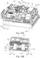
- the device 1 includes a control card 110 which is superimposed on the power card and which includes one or more microcontrollers or analog circuits to manage the operation of the device 1.
- An HMI interface card 120 is placed above the control card 110 and includes a display 121 as well as several control buttons 122 carried by a plate 129.
- the device 1 also includes cards 130 to 133 which carry connectors and terminal blocks accessible from the side and lower faces of the housing.
- These cards 130 to 133 are oriented perpendicular to the power cards 30 and control cards 110.
- the lower part 40 of the housing is made with openings 46 for the outlet of the connectors and terminal blocks.
- Device 1 also includes a card 190 which carries terminal blocks and connectors, and which is located on the side of device 1 opposite to card 130.
- the card 190 includes a printed circuit board 191 which extends parallel to the interior face of the radiator 10 between the latter and the board 38 of the power card 30.
- the board 191 is fixed on the board 38 using of spacers 193.
- the plate 191 carries connectors and/or terminal blocks 195.
- the device 1 comprises a part 100 which is used to fix a terminal connected to the electrical mass and/or to earth.
- This part 100 is accessible laterally thanks to a corresponding opening 45 made on the lower part 40 of the housing, and has a tapped hole 101 for fixing a screw holding the terminal.
- Part 100 is fixed to radiator 10 by two screws 102, visible on the figure 5 . These screws 102 ensure electrical contact between the radiator 10 and the part 100.
- the screws 102 have heads 104 which apply to corresponding conductive tracks of the power card 30, so as to electrically connect these tracks to the radiator 10 and to the mass and/or earth lug.
- the part 100 thus plays a dual function, namely on the one hand ensuring the electrical connection between the radiator 10 and the power card 30 and an external connection by terminal, and on the other hand a mechanical fixing of the power card 30 on the radiator 10.
- the use of a single part performing this dual function contributes to the compactness of the device.
- the upper part 50 of the housing comprises, as can be seen in the Figure 9 in particular, an opening 51 for the screen 121 and holes 52 for the buttons 122.
- a housing 53 is provided to receive an additional module 140, visible on the figure 8 , provided with a connector which connects to the control card through an opening 56 opening into the bottom of the housing 53.
- Housing 53 is closed by a hatch 150, visible on the Figure 7 in particular, which is fixed on the upper part 50 by a tab 151 provided with a screw which engages in a corresponding thread 57 provided on the upper part 50.
- Means such as a tamper-evident label can be placed at the level of the hatch 150 to signal the removal of the latter.
- the HMI interface card 120 carries a reader defining a slot 124 for a memory card M, for example of the "micro SD" type, which opens into a recess 58 in the upper part 50 designed to accommodate the tab 151 for locking the hatch 150 .
- the device 1 can be configured to record various operating parameters in the memory card M, and thus have a useful history for carrying out a diagnosis in the event of a breakdown, for example.
- the M memory card may still be useful for firmware update operations or for downloading application-specific settings.
- the HMI 120 interface card can also carry, as seen in the Figure 10 in particular, one or more front connectors 127, for example of the RJ45 or USB type.
- the presence of these connectors accessible on the front facilitates updating, programming and diagnostic operations of the device 1 by an operator.
- connectors 127 are carried by extensions 128 of the printed circuit board 129 of the card 120, which extend on either side of the recess 58, thus contributing to the compactness of the mounting of the card 120 in the housing. the device 1.
- the device 1 can include, as seen in the Figure 10A , a backup battery 160 connected by an electrical cable 162 to the control card 110.
- This backup battery 160 is flat and oriented perpendicular to the control card 110, being housed in a corresponding housing 161 provided in the upper part 50 of the housing next to housing 53 receiving the additional module 140.
- FIG. 13 a power half-bridge used to carry out PWM type regulation when the device 1 is an alternator regulator, this half-bridge being connected by terminals 230 and 232 to the inductor L of the alternator.
- This figure also shows schematically a control circuit 240, belonging for example to the control card 110, and capable of generating a control signal 241.
- the half-bridge shown in figure 13 presents a redundancy of the controlled power components, in order to ensure the control and supply of the excitation current even in the event of failure of one of these components, for example short circuit of a transistor or permanent blocking of the transistor.
- the half-bridge comprises a first pair TH1 and TH2 of power transistors, electrically connected in parallel between the + terminal of the DC bus 310 and the terminal 230 of the inductor L.
- Two freewheeling diodes DL1 and DL2 are connected in parallel between terminal 230 of inductor L and terminal - of the DC bus. Diodes DL1 and DL2 have their cathode connected to terminal 230.
- the half-bridge comprises a second pair TB1, TB2 of power transistors electrically connected in parallel between terminal - of the DC bus and terminal 232 of the inductor L.
- Two diodes DF1 and DF2 are arranged in parallel between terminal 232 and the + terminal of the DC bus, with their cathode connected to this + terminal of the bus.
- Monitoring is ensured for example by the control circuit 240, in order to verify that the transistors TH1, TH2, TB1, TB2 operate without failure. For example, the voltage across the inductor L is monitored by device 1 to verify that it corresponds to the PWM command.
- transistor TB1 In normal operation, in the absence of transistor failure, transistor TB1 is driven in permanent saturated mode and TB2 is kept blocked on standby. Only the transistor TH1 receives the control signal 241, the transistor TH2 being maintained in waiting blocked.
- the transistor TH1 When the transistor TH1 is driven into conduction, the current passes through this transistor, through the inductor and through the transistor TB1. When transistor TH1 is blocked, the current flowing in the inductor circulates in a loop in the transistor TB1 and in the freewheeling diodes DL1 and DL2.
- transistor TH2 is driven saturated to maintain the short circuit in parallel with TH1 and the PWM command is sent to TB1; TB2 is kept blocked.
- transistor TH1 is driven off in order to avoid potential erratic switching, and transistor TH2 receives the PWM command to replace TH1.
- TB1 is maintained in the saturated state and TB2 in the blocked state.
- transistor TB 1 is controlled blocked to avoid possible erratic switching.
- Transistor TB2 receives the saturated command replacing TB1.
- Transistor TH1 continues to receive the PWM command and transistor TH2 is driven off.
- the transistors TB1, TB2, TH1 and TH2 belong to a monolithic power module 90, shown in Figure 14 , which comprises seven transistors, being marketed for another application, these transistors being distributed into three parallel branches 301, 302, 303 each comprising two transistors in series and a seventh transistor in parallel with the three branches, in series with a diode 305.
- transistors of module 90 which can be used to constitute transistors TB1, TB2, TH1 and TH2.
- the invention is not limited to the example which has just been described.
- the power stage can be produced with discrete components instead of a module grouping them together.
Landscapes
- Engineering & Computer Science (AREA)
- Power Engineering (AREA)
- Microelectronics & Electronic Packaging (AREA)
- Physics & Mathematics (AREA)
- Thermal Sciences (AREA)
- Control Of Eletrric Generators (AREA)
- Dc-Dc Converters (AREA)
- Rectifiers (AREA)
Claims (12)
- Elektronische Vorrichtung, insbesondere Generatorregler, aufweisend eine Leistungsstufe zur Verbindung mit einer induktiven Last, insbesondere mit einem Generatorinduktor, mit wenigstens einem ersten Paar Leistungstransistoren (TH1, TH2), die mit einer Klemme (+) eines Gleichstrombusses verbunden sind, einem zweiten Paar Transistoren (TB1, TB2) und einer Steuerschaltung (240) für diese Transistoren, die Transistoren des ersten Transistorenpaars (TH1, TH2) sind parallel zwischen der Klemme (+) des Gleichstrombusses und einem ersten Ausgang (230) angeordnet, der mit der Last (L) zu verbinden ist, wobei wenigstens eine Freilaufdiode (DL1, DL2) die entgegengesetzte Klemme (-) des Gleichstrombusses mit dem ersten Ausgang (230) verbindet, die Transistoren des zweiten Transistorenpaars (TB1, TB2) sind parallel zwischen einen zweiten Ausgang (232) zur Verbindung mit der Last (L) und die entgegengesetzte Klemme (-) des Gleichstrombusses geschaltet, wobei wenigstens eine Diode (DF1, DF2) den zweiten Ausgang (232) mit der Klemme (+) des Gleichstrombusses verbindet, wobei wenigstens einer (TB1) der Transistoren des zweiten Paars so von der Steuerschaltung (240) angesteuert wird, dass er während des Normalbetriebs des Geräts durchlässig ist, die Steuerschaltung (240) ist dafür angeordnet, ein gepulstes Steuersignal zu erzeugen, mit dem der Strom in der Last geregelt werden kann, und einen Ausfall eines der Transistoren zu detektieren, wobei die Steuerschaltung während des Normalbetriebs ohne Ausfall der Transistoren dafür angeordnet ist, das Steuersignal (241) an einen (TH1) der Transistoren des ersten Paars zu senden, wobei sie den anderen Transistor (TH2) dieses Paars in einem gesperrten Zustand hält, dadurch gekennzeichnet, dass die Steuerschaltung dafür angeordnet ist, im Falle eines Ausfalls eines Transistors (TH1) des ersten Paars (TH1, TH2), wodurch er kurzgeschlossen bleibt, den zweiten Transistor (TH2) dieses Paars anzusteuern, um ihn zu sättigen, einen Transistor (TB2) des anderen Paars (TB1, TB2) im gesperrten Zustand zu halten und das gepulste Steuersignal an den anderen Transistor (TB1) dieses zweiten Paars (TB1, TB2) zu senden.
- Vorrichtung nach Anspruch 1, wobei die Steuerschaltung dafür angeordnet ist, im Falle eines Ausfalls eines Transistors (TH1) des ersten Paars, wodurch er im Leerlauf bleibt, das gepulste Steuersignal an den anderen Transistor (TH2) dieses Paars zu senden.
- Vorrichtung nach einem der vorhergehenden Ansprüche, wobei der andere Transistor (TB2) des zweiten Paars so von der Steuerschaltung (240) gesteuert wird, dass er während des Normalbetriebs gesperrt ist.
- Vorrichtung nach einem der vorhergehenden Ansprüche, wobei die Steuerschaltung dafür angeordnet ist, im Falle eines Ausfalls eines (TB1) der Transistoren des zweiten Paars, wodurch er im Leerlauf bleibt, den anderen Transistor (TB2) dieses Paars anzusteuern, um ihn zu sättigen.
- Vorrichtung nach einem der Ansprüche 1 bis 4, aufweisend zwei parallele Freilaufdioden (DL1, DL2).
- Vorrichtung nach einem der Ansprüche 1 bis 5, aufweisend zwei parallele Dioden (DF1, DF2), die den zweiten Ausgang (232) mit der Klemme (+) des Gleichstrombusses verbinden.
- Vorrichtung nach einem der vorhergehenden Ansprüche, die dafür angeordnet ist, im Negativ-Forcing-Modus zu arbeiten, wenn der Strom in der Last zu Regelungszwecken schnell aufgehoben werden muss, wobei in diesem Modus die Transistoren des ersten Paars (TH1, TH2) gesperrt angesteuert werden und die zwei Transistoren des zweiten Paars (TB1, TB2) ebenfalls.
- Vorrichtung nach einem der Ansprüche 1 bis 7, wobei das gepulste Steuersignal ein PWM- (Pulse Width Modulation) Signal ist.
- Vorrichtung nach einem der Ansprüche 1 bis 8, wobei die Transistoren des ersten Paars zu einem Leistungsmodul (90) gehören, das drei parallele Zweige (301, 302, 303), wobei jeder Zweig zwei Transistoren in Reihe umfasst, und einen siebten Transistor in Reihe mit einer Diode (304) umfasst, wobei die Anordnung, die von diesem Transistor in Reihe mit der Diode gebildet ist, mit den drei Zweigen parallel geschaltet ist, wobei die Transistoren (TH1; TH2) des ersten Paars jeweils innerhalb eines jeweiligen Zweigs (302; 301) aufgenommen sind.
- Vorrichtung nach Anspruch 9, wobei einer (TB1) der Transistoren des zweiten Paars aus dem verbleibenden Zweig (303) gewählt ist und der andere Transistor (TB2) von dem Transistor gebildet ist, der sich in Reihe mit der Diode (305) befindet.
- Vorrichtung nach einem der Ansprüche 1 bis 10, wobei die Transistoren (TB1, TB2, TH1, TH2) IGBTs oder MOSFETs, vorzugsweise IGBTs sind.
- Verfahren zur Regelung eines Generators, wobei der Induktor des Generators mit den Ausgängen einer Reglers verbunden ist, der Folgendes aufweist:- eine Leistungsstufe mit:o einem ersten Paar Leistungstransistoren (TH1, TH2), die zwischen einer Klemme (+) eines Gleichstrombusses und einer ersten Klemme des Induktors parallel geschaltet sind,o einem zweiten Paar Transistoren (TB1, TB2), die zwischen einer zweiten Klemme (232) des Induktors und einer entgegengesetzten Klemme (-) des Gleichstrombusses parallel geschaltet sind,o wenigstens einer Diode (DF1, DF2), die die zweite Klemme (232) des Induktors mit der Klemme (+) des Gleichstrombusses verbindet,o wenigstens einer Freilaufdiode (DL1, DL2), die die entgegengesetzte Klemme (-) des Gleichstrombusses mit der ersten Klemme (230) des Induktors (L) verbindet,- eine Steuerschaltung (240), die dafür angeordnet ist, ein gepulstes Steuersignal zu erzeugen, mit dem der Strom im Induktor geregelt werden kann, und einen Ausfall eines der Transistoren zu detektieren,wobei bei dem Verfahren:- während des Normalbetriebs des Reglers wenigstens einer (TB1) der Transistoren des zweiten Paars so von der Steuerschaltung (240) angesteuert wird, dass er durchlässig ist, das Steuersignal (241) an einen (TH1) der Transistoren des ersten Paars gesendet wird, wobei der andere Transistor (TH2) dieses Paars in einem gesperrten Zustand gehalten wird,- bei Anforderung einer schnellen Aufhebung des Stroms im Induktor zu Regelungszwecken die Transistoren des ersten Paars (TH1, TH2) und die Transistoren des zweiten Paars (TB1, TB2) gesperrt angesteuert werden,- im Falle eines Ausfalls eines Transistors (TH1) des ersten Paars, wodurch er im Leerlauf bleibt, zu Zwecken der Regelung des Stroms im Induktor das gepulste Steuersignal an den anderen Transistor (TH2) dieses Paars gesendet wird,- im Falle eines Ausfalls eines (TB1) der Transistoren des zweiten Paars, wodurch er im Leerlauf bleibt, der andere Transistor (TB2) dieses Paars angesteuert wird, um ihn zu sättigen, dadurch gekennzeichnet, dass- im Falle eines Ausfalls eines Transistors (TH1) des ersten Paars (TH1, TH2), wodurch er kurzgeschlossen bleibt, der zweite Transistor (TH2) dieses Paars angesteuert wird, um ihn zu sättigen, ein Transistor (TB2) des anderen Paars (TB1, TB2) im gesperrten Zustand gehalten wird und das gepulste Steuersignal zu Zwecken der Regelung des Stroms im Induktor an den anderen Transistor (TB1) dieses zweiten Paars (TB1, TB2) gesendet wird.
Applications Claiming Priority (2)
| Application Number | Priority Date | Filing Date | Title |
|---|---|---|---|
| FR1750486A FR3062259B1 (fr) | 2017-01-20 | 2017-01-20 | Dispositif electronique, notamment regulateur d'alternateur, et procede de regulation d'un tel dispositif |
| PCT/EP2018/050928 WO2018134171A1 (fr) | 2017-01-20 | 2018-01-16 | Dispositif electronique, notamment regulateur d'alternateur, et procede de regulation d'un tel dispositif |
Publications (2)
| Publication Number | Publication Date |
|---|---|
| EP3571760A1 EP3571760A1 (de) | 2019-11-27 |
| EP3571760B1 true EP3571760B1 (de) | 2023-10-18 |
Family
ID=59152977
Family Applications (1)
| Application Number | Title | Priority Date | Filing Date |
|---|---|---|---|
| EP18700357.9A Active EP3571760B1 (de) | 2017-01-20 | 2018-01-16 | Elektronische vorrichtung, insbesondere ein lichtmaschinenregler, und verfahren zur regelung solch einer vorrichtung |
Country Status (7)
| Country | Link |
|---|---|
| US (1) | US11171590B2 (de) |
| EP (1) | EP3571760B1 (de) |
| CN (1) | CN110192340B (de) |
| DK (1) | DK3571760T3 (de) |
| ES (1) | ES2967446T3 (de) |
| FR (1) | FR3062259B1 (de) |
| WO (1) | WO2018134171A1 (de) |
Families Citing this family (5)
| Publication number | Priority date | Publication date | Assignee | Title |
|---|---|---|---|---|
| WO2014210125A1 (en) * | 2013-06-26 | 2014-12-31 | Siemens Industry, Inc. | Printed circuit board power cell |
| FR3062276B1 (fr) * | 2017-01-20 | 2019-06-07 | Moteurs Leroy-Somer | Dispositif electronique, notamment variateur de vitesse ou regulateur d'alternateur, comportant un dissipateur thermique et une carte de puissance |
| FR3062275B1 (fr) * | 2017-01-20 | 2019-06-07 | Moteurs Leroy-Somer | Ensemble comportant un dispositif electronique, notamment variateur de vitesse ou regulateur d'alternateur et deux ensembles d'elements de formes differentes pour la fixation du dispositif |
| TWI768917B (zh) * | 2021-05-21 | 2022-06-21 | 緯創資通股份有限公司 | 插座組件及包含其之介面卡與電子裝置 |
| JP2024022219A (ja) * | 2022-08-05 | 2024-02-16 | キオクシア株式会社 | 半導体記憶装置 |
Family Cites Families (18)
| Publication number | Priority date | Publication date | Assignee | Title |
|---|---|---|---|---|
| US5739676A (en) * | 1996-11-04 | 1998-04-14 | Ford Motor Company | Multiple-alternator electrical system |
| CN101202528B (zh) | 2006-12-11 | 2012-10-10 | 丹佛斯传动有限公司 | 电子装置及电动机变频器 |
| FR2910197B1 (fr) * | 2006-12-13 | 2009-02-06 | Messier Dowty Sa Sa | Alimentation a deux onduleurs en serie pour actionneur electromecanique polyphase |
| DE102008037064A1 (de) * | 2008-08-08 | 2010-02-11 | Bayerische Motoren Werke Aktiengesellschaft | Schaltungsanordnung für einen elektrischen Antrieb |
| US7893560B2 (en) * | 2008-09-12 | 2011-02-22 | Nellcor Puritan Bennett Llc | Low power isolation design for a multiple sourced power bus |
| CN101478229A (zh) * | 2008-09-28 | 2009-07-08 | 南京航空航天大学 | 一种用于开关磁阻电机的容错功率变换器 |
| US20100258206A1 (en) * | 2009-04-10 | 2010-10-14 | Baker Donald C | Sump extension assembly for preventing suction entrapment |
| FR2949914B1 (fr) * | 2009-09-07 | 2014-11-21 | Valeo Equip Electr Moteur | Alternateur a redressement synchrone pour vehicule automobile, equipe de moyens electroniques de gestion de defauts |
| FR2973640B1 (fr) | 2011-04-04 | 2013-04-05 | Schneider Toshiba Inverter Europe Sas | Variateur de vitesse a architecture optimisee |
| US20140313797A1 (en) * | 2011-11-15 | 2014-10-23 | Alstom Technology Ltd. | Power electronic module |
| JP5606506B2 (ja) * | 2012-09-20 | 2014-10-15 | 三菱電機株式会社 | 駆動制御装置及び駆動制御方法 |
| CN203166814U (zh) * | 2012-12-13 | 2013-08-28 | 北京中纺锐力机电有限公司 | 一种开关磁阻电机控制器的主功率电路 |
| EP2747270B1 (de) * | 2012-12-21 | 2014-10-15 | Inmotion Technologies AB | Brückenzweig |
| JP5657716B2 (ja) | 2013-01-15 | 2015-01-21 | ファナック株式会社 | 放熱器を備えたモータ駆動装置 |
| CN103812319B (zh) * | 2014-02-25 | 2016-08-17 | 南京航空航天大学 | 一种四相无刷直流电机容错功率变换器及控制方法 |
| CN205430848U (zh) | 2015-10-14 | 2016-08-03 | 孚瑞肯电气(深圳)有限公司 | 一种散热器 |
| CN105356816B (zh) * | 2015-12-01 | 2017-09-29 | 浙江大学 | 基于继电器网络的开关磁阻电机多类型故障容错系统 |
| CN105939134B (zh) * | 2016-06-15 | 2018-04-03 | 浙江大学 | 基于单个功率变换器驱动的双开关磁阻电机运行控制系统 |
-
2017
- 2017-01-20 FR FR1750486A patent/FR3062259B1/fr active Active
-
2018
- 2018-01-16 ES ES18700357T patent/ES2967446T3/es active Active
- 2018-01-16 EP EP18700357.9A patent/EP3571760B1/de active Active
- 2018-01-16 US US16/478,728 patent/US11171590B2/en active Active
- 2018-01-16 DK DK18700357.9T patent/DK3571760T3/da active
- 2018-01-16 CN CN201880007352.6A patent/CN110192340B/zh active Active
- 2018-01-16 WO PCT/EP2018/050928 patent/WO2018134171A1/fr not_active Ceased
Also Published As
| Publication number | Publication date |
|---|---|
| ES2967446T3 (es) | 2024-04-30 |
| WO2018134171A1 (fr) | 2018-07-26 |
| DK3571760T3 (da) | 2024-01-08 |
| FR3062259B1 (fr) | 2019-06-07 |
| CN110192340A (zh) | 2019-08-30 |
| US11171590B2 (en) | 2021-11-09 |
| EP3571760A1 (de) | 2019-11-27 |
| US20200052630A1 (en) | 2020-02-13 |
| CN110192340B (zh) | 2023-12-08 |
| FR3062259A1 (fr) | 2018-07-27 |
Similar Documents
| Publication | Publication Date | Title |
|---|---|---|
| EP3571760B1 (de) | Elektronische vorrichtung, insbesondere ein lichtmaschinenregler, und verfahren zur regelung solch einer vorrichtung | |
| FR3062276B1 (fr) | Dispositif electronique, notamment variateur de vitesse ou regulateur d'alternateur, comportant un dissipateur thermique et une carte de puissance | |
| FR3062277B1 (fr) | Dispositif electronique, notamment variateur de vitesse ou regulateur d'alternateur, comportant au moins un composant de puissance et une pluralite de condensateurs | |
| FR3068841B1 (fr) | Dispositif de commutation electrique et coffre de traction electrique associe | |
| EP3381114B1 (de) | Modulares system zur umwandlung von gleichstrom in dreiphasigen strom | |
| FR3062274B1 (fr) | Dispositif electronique, notamment variateur de vitesse ou regulateur d'alternateur, comportant un logement de reception d'un module annexe | |
| FR3062275B1 (fr) | Ensemble comportant un dispositif electronique, notamment variateur de vitesse ou regulateur d'alternateur et deux ensembles d'elements de formes differentes pour la fixation du dispositif | |
| EP3056070B1 (de) | Elektrisches modul, elektrischen system mit derartigem elektrischen modul und zugehörige herstellungsverfahren | |
| WO2019122117A1 (fr) | Systeme de controle d'une machine electrique tournante | |
| EP1912261A1 (de) | Elektrische Anschlussvorrichtung, insbesondere für elektrischen Sonnenkollektor | |
| FR2752109A1 (fr) | Dissipateur pour pont redresseur d'alternateur de vehicule automobile, ensemble redresseur et alternateur comportant de tels dissipateurs | |
| EP3476036B1 (de) | System und verfahren zur umwandlung von gleichstrom in dreiphasigen wechselstrom mit einem luftradiator | |
| EP3448139B1 (de) | Elektronische ausrüstung, die einen befestigungsflansch umfasst | |
| EP2351193B1 (de) | Gleichrichtersvorrichtung für eine drehende elektrische machine und drehende elektrische maschine mit einer solchen vorrichtung | |
| FR2936915A1 (fr) | Machine electrique tournante comportant un agencement de redressement de courant et de regulation de tension. | |
| FR2928784A1 (fr) | Dispositif de raccordement electrique notamment pour panneau solaire electrique | |
| EP3895511A1 (de) | Spannungswandler und verfahren zur herstellung eines spannungswandlers | |
| EP3221952B1 (de) | Wechselstrom-gleichstrom-wandler | |
| FR3040526A1 (fr) | Element de commutation pour plaque de distribution d'energie electrique et boitier de distribution d'energie electrique dote d'un tel element de commutation | |
| FR3029032A1 (fr) | Convertisseur alternatif-continu |
Legal Events
| Date | Code | Title | Description |
|---|---|---|---|
| STAA | Information on the status of an ep patent application or granted ep patent |
Free format text: STATUS: UNKNOWN |
|
| STAA | Information on the status of an ep patent application or granted ep patent |
Free format text: STATUS: THE INTERNATIONAL PUBLICATION HAS BEEN MADE |
|
| PUAI | Public reference made under article 153(3) epc to a published international application that has entered the european phase |
Free format text: ORIGINAL CODE: 0009012 |
|
| STAA | Information on the status of an ep patent application or granted ep patent |
Free format text: STATUS: REQUEST FOR EXAMINATION WAS MADE |
|
| 17P | Request for examination filed |
Effective date: 20190820 |
|
| AK | Designated contracting states |
Kind code of ref document: A1 Designated state(s): AL AT BE BG CH CY CZ DE DK EE ES FI FR GB GR HR HU IE IS IT LI LT LU LV MC MK MT NL NO PL PT RO RS SE SI SK SM TR |
|
| AX | Request for extension of the european patent |
Extension state: BA ME |
|
| DAV | Request for validation of the european patent (deleted) | ||
| DAX | Request for extension of the european patent (deleted) | ||
| STAA | Information on the status of an ep patent application or granted ep patent |
Free format text: STATUS: EXAMINATION IS IN PROGRESS |
|
| 17Q | First examination report despatched |
Effective date: 20200708 |
|
| RIC1 | Information provided on ipc code assigned before grant |
Ipc: H02K 11/05 20160101ALI20221214BHEP Ipc: H02M 7/538 20070101ALI20221214BHEP Ipc: H02H 7/00 20060101ALI20221214BHEP Ipc: H02P 9/12 20060101AFI20221214BHEP |
|
| GRAP | Despatch of communication of intention to grant a patent |
Free format text: ORIGINAL CODE: EPIDOSNIGR1 |
|
| STAA | Information on the status of an ep patent application or granted ep patent |
Free format text: STATUS: GRANT OF PATENT IS INTENDED |
|
| INTG | Intention to grant announced |
Effective date: 20230206 |
|
| GRAJ | Information related to disapproval of communication of intention to grant by the applicant or resumption of examination proceedings by the epo deleted |
Free format text: ORIGINAL CODE: EPIDOSDIGR1 |
|
| STAA | Information on the status of an ep patent application or granted ep patent |
Free format text: STATUS: EXAMINATION IS IN PROGRESS |
|
| INTC | Intention to grant announced (deleted) | ||
| GRAP | Despatch of communication of intention to grant a patent |
Free format text: ORIGINAL CODE: EPIDOSNIGR1 |
|
| STAA | Information on the status of an ep patent application or granted ep patent |
Free format text: STATUS: GRANT OF PATENT IS INTENDED |
|
| INTG | Intention to grant announced |
Effective date: 20230524 |
|
| GRAS | Grant fee paid |
Free format text: ORIGINAL CODE: EPIDOSNIGR3 |
|
| GRAA | (expected) grant |
Free format text: ORIGINAL CODE: 0009210 |
|
| STAA | Information on the status of an ep patent application or granted ep patent |
Free format text: STATUS: THE PATENT HAS BEEN GRANTED |
|
| AK | Designated contracting states |
Kind code of ref document: B1 Designated state(s): AL AT BE BG CH CY CZ DE DK EE ES FI FR GB GR HR HU IE IS IT LI LT LU LV MC MK MT NL NO PL PT RO RS SE SI SK SM TR |
|
| REG | Reference to a national code |
Ref country code: GB Ref legal event code: FG4D Free format text: NOT ENGLISH |
|
| REG | Reference to a national code |
Ref country code: CH Ref legal event code: EP |
|
| REG | Reference to a national code |
Ref country code: DE Ref legal event code: R096 Ref document number: 602018059513 Country of ref document: DE |
|
| REG | Reference to a national code |
Ref country code: IE Ref legal event code: FG4D Free format text: LANGUAGE OF EP DOCUMENT: FRENCH |
|
| REG | Reference to a national code |
Ref country code: DK Ref legal event code: T3 Effective date: 20240105 |
|
| REG | Reference to a national code |
Ref country code: NO Ref legal event code: T2 Effective date: 20231018 |
|
| REG | Reference to a national code |
Ref country code: LT Ref legal event code: MG9D |
|
| REG | Reference to a national code |
Ref country code: NL Ref legal event code: MP Effective date: 20231018 |
|
| REG | Reference to a national code |
Ref country code: AT Ref legal event code: MK05 Ref document number: 1623362 Country of ref document: AT Kind code of ref document: T Effective date: 20231018 |
|
| PG25 | Lapsed in a contracting state [announced via postgrant information from national office to epo] |
Ref country code: NL Free format text: LAPSE BECAUSE OF FAILURE TO SUBMIT A TRANSLATION OF THE DESCRIPTION OR TO PAY THE FEE WITHIN THE PRESCRIBED TIME-LIMIT Effective date: 20231018 |
|
| PG25 | Lapsed in a contracting state [announced via postgrant information from national office to epo] |
Ref country code: GR Free format text: LAPSE BECAUSE OF FAILURE TO SUBMIT A TRANSLATION OF THE DESCRIPTION OR TO PAY THE FEE WITHIN THE PRESCRIBED TIME-LIMIT Effective date: 20240119 |
|
| PG25 | Lapsed in a contracting state [announced via postgrant information from national office to epo] |
Ref country code: IS Free format text: LAPSE BECAUSE OF FAILURE TO SUBMIT A TRANSLATION OF THE DESCRIPTION OR TO PAY THE FEE WITHIN THE PRESCRIBED TIME-LIMIT Effective date: 20240218 |
|
| PG25 | Lapsed in a contracting state [announced via postgrant information from national office to epo] |
Ref country code: LT Free format text: LAPSE BECAUSE OF FAILURE TO SUBMIT A TRANSLATION OF THE DESCRIPTION OR TO PAY THE FEE WITHIN THE PRESCRIBED TIME-LIMIT Effective date: 20231018 |
|
| PG25 | Lapsed in a contracting state [announced via postgrant information from national office to epo] |
Ref country code: AT Free format text: LAPSE BECAUSE OF FAILURE TO SUBMIT A TRANSLATION OF THE DESCRIPTION OR TO PAY THE FEE WITHIN THE PRESCRIBED TIME-LIMIT Effective date: 20231018 |
|
| PG25 | Lapsed in a contracting state [announced via postgrant information from national office to epo] |
Ref country code: LT Free format text: LAPSE BECAUSE OF FAILURE TO SUBMIT A TRANSLATION OF THE DESCRIPTION OR TO PAY THE FEE WITHIN THE PRESCRIBED TIME-LIMIT Effective date: 20231018 Ref country code: IS Free format text: LAPSE BECAUSE OF FAILURE TO SUBMIT A TRANSLATION OF THE DESCRIPTION OR TO PAY THE FEE WITHIN THE PRESCRIBED TIME-LIMIT Effective date: 20240218 Ref country code: GR Free format text: LAPSE BECAUSE OF FAILURE TO SUBMIT A TRANSLATION OF THE DESCRIPTION OR TO PAY THE FEE WITHIN THE PRESCRIBED TIME-LIMIT Effective date: 20240119 Ref country code: BG Free format text: LAPSE BECAUSE OF FAILURE TO SUBMIT A TRANSLATION OF THE DESCRIPTION OR TO PAY THE FEE WITHIN THE PRESCRIBED TIME-LIMIT Effective date: 20240118 Ref country code: AT Free format text: LAPSE BECAUSE OF FAILURE TO SUBMIT A TRANSLATION OF THE DESCRIPTION OR TO PAY THE FEE WITHIN THE PRESCRIBED TIME-LIMIT Effective date: 20231018 Ref country code: PT Free format text: LAPSE BECAUSE OF FAILURE TO SUBMIT A TRANSLATION OF THE DESCRIPTION OR TO PAY THE FEE WITHIN THE PRESCRIBED TIME-LIMIT Effective date: 20240219 |
|
| REG | Reference to a national code |
Ref country code: ES Ref legal event code: FG2A Ref document number: 2967446 Country of ref document: ES Kind code of ref document: T3 Effective date: 20240430 |
|
| PG25 | Lapsed in a contracting state [announced via postgrant information from national office to epo] |
Ref country code: SE Free format text: LAPSE BECAUSE OF FAILURE TO SUBMIT A TRANSLATION OF THE DESCRIPTION OR TO PAY THE FEE WITHIN THE PRESCRIBED TIME-LIMIT Effective date: 20231018 Ref country code: RS Free format text: LAPSE BECAUSE OF FAILURE TO SUBMIT A TRANSLATION OF THE DESCRIPTION OR TO PAY THE FEE WITHIN THE PRESCRIBED TIME-LIMIT Effective date: 20231018 Ref country code: PL Free format text: LAPSE BECAUSE OF FAILURE TO SUBMIT A TRANSLATION OF THE DESCRIPTION OR TO PAY THE FEE WITHIN THE PRESCRIBED TIME-LIMIT Effective date: 20231018 Ref country code: LV Free format text: LAPSE BECAUSE OF FAILURE TO SUBMIT A TRANSLATION OF THE DESCRIPTION OR TO PAY THE FEE WITHIN THE PRESCRIBED TIME-LIMIT Effective date: 20231018 Ref country code: HR Free format text: LAPSE BECAUSE OF FAILURE TO SUBMIT A TRANSLATION OF THE DESCRIPTION OR TO PAY THE FEE WITHIN THE PRESCRIBED TIME-LIMIT Effective date: 20231018 |
|
| REG | Reference to a national code |
Ref country code: DE Ref legal event code: R097 Ref document number: 602018059513 Country of ref document: DE |
|
| PG25 | Lapsed in a contracting state [announced via postgrant information from national office to epo] |
Ref country code: SK Free format text: LAPSE BECAUSE OF FAILURE TO SUBMIT A TRANSLATION OF THE DESCRIPTION OR TO PAY THE FEE WITHIN THE PRESCRIBED TIME-LIMIT Effective date: 20231018 |
|
| PG25 | Lapsed in a contracting state [announced via postgrant information from national office to epo] |
Ref country code: SM Free format text: LAPSE BECAUSE OF FAILURE TO SUBMIT A TRANSLATION OF THE DESCRIPTION OR TO PAY THE FEE WITHIN THE PRESCRIBED TIME-LIMIT Effective date: 20231018 Ref country code: SK Free format text: LAPSE BECAUSE OF FAILURE TO SUBMIT A TRANSLATION OF THE DESCRIPTION OR TO PAY THE FEE WITHIN THE PRESCRIBED TIME-LIMIT Effective date: 20231018 Ref country code: RO Free format text: LAPSE BECAUSE OF FAILURE TO SUBMIT A TRANSLATION OF THE DESCRIPTION OR TO PAY THE FEE WITHIN THE PRESCRIBED TIME-LIMIT Effective date: 20231018 Ref country code: EE Free format text: LAPSE BECAUSE OF FAILURE TO SUBMIT A TRANSLATION OF THE DESCRIPTION OR TO PAY THE FEE WITHIN THE PRESCRIBED TIME-LIMIT Effective date: 20231018 |
|
| REG | Reference to a national code |
Ref country code: DE Ref legal event code: R119 Ref document number: 602018059513 Country of ref document: DE |
|
| PLBE | No opposition filed within time limit |
Free format text: ORIGINAL CODE: 0009261 |
|
| STAA | Information on the status of an ep patent application or granted ep patent |
Free format text: STATUS: NO OPPOSITION FILED WITHIN TIME LIMIT |
|
| PG25 | Lapsed in a contracting state [announced via postgrant information from national office to epo] |
Ref country code: MC Free format text: LAPSE BECAUSE OF FAILURE TO SUBMIT A TRANSLATION OF THE DESCRIPTION OR TO PAY THE FEE WITHIN THE PRESCRIBED TIME-LIMIT Effective date: 20231018 |
|
| PG25 | Lapsed in a contracting state [announced via postgrant information from national office to epo] |
Ref country code: MC Free format text: LAPSE BECAUSE OF FAILURE TO SUBMIT A TRANSLATION OF THE DESCRIPTION OR TO PAY THE FEE WITHIN THE PRESCRIBED TIME-LIMIT Effective date: 20231018 |
|
| PG25 | Lapsed in a contracting state [announced via postgrant information from national office to epo] |
Ref country code: LU Free format text: LAPSE BECAUSE OF NON-PAYMENT OF DUE FEES Effective date: 20240116 |
|
| 26N | No opposition filed |
Effective date: 20240719 |
|
| PG25 | Lapsed in a contracting state [announced via postgrant information from national office to epo] |
Ref country code: LU Free format text: LAPSE BECAUSE OF NON-PAYMENT OF DUE FEES Effective date: 20240116 |
|
| PG25 | Lapsed in a contracting state [announced via postgrant information from national office to epo] |
Ref country code: DE Free format text: LAPSE BECAUSE OF NON-PAYMENT OF DUE FEES Effective date: 20240801 |
|
| PG25 | Lapsed in a contracting state [announced via postgrant information from national office to epo] |
Ref country code: BE Free format text: LAPSE BECAUSE OF NON-PAYMENT OF DUE FEES Effective date: 20240131 |
|
| PG25 | Lapsed in a contracting state [announced via postgrant information from national office to epo] |
Ref country code: SI Free format text: LAPSE BECAUSE OF FAILURE TO SUBMIT A TRANSLATION OF THE DESCRIPTION OR TO PAY THE FEE WITHIN THE PRESCRIBED TIME-LIMIT Effective date: 20231018 |
|
| PG25 | Lapsed in a contracting state [announced via postgrant information from national office to epo] |
Ref country code: SI Free format text: LAPSE BECAUSE OF FAILURE TO SUBMIT A TRANSLATION OF THE DESCRIPTION OR TO PAY THE FEE WITHIN THE PRESCRIBED TIME-LIMIT Effective date: 20231018 Ref country code: DE Free format text: LAPSE BECAUSE OF NON-PAYMENT OF DUE FEES Effective date: 20240801 Ref country code: BE Free format text: LAPSE BECAUSE OF NON-PAYMENT OF DUE FEES Effective date: 20240131 |
|
| REG | Reference to a national code |
Ref country code: BE Ref legal event code: MM Effective date: 20240131 |
|
| PG25 | Lapsed in a contracting state [announced via postgrant information from national office to epo] |
Ref country code: IE Free format text: LAPSE BECAUSE OF NON-PAYMENT OF DUE FEES Effective date: 20240116 |
|
| PG25 | Lapsed in a contracting state [announced via postgrant information from national office to epo] |
Ref country code: IE Free format text: LAPSE BECAUSE OF NON-PAYMENT OF DUE FEES Effective date: 20240116 |
|
| PGFP | Annual fee paid to national office [announced via postgrant information from national office to epo] |
Ref country code: CH Payment date: 20250201 Year of fee payment: 8 |
|
| PGFP | Annual fee paid to national office [announced via postgrant information from national office to epo] |
Ref country code: CZ Payment date: 20250109 Year of fee payment: 8 |
|
| PG25 | Lapsed in a contracting state [announced via postgrant information from national office to epo] |
Ref country code: CY Free format text: LAPSE BECAUSE OF FAILURE TO SUBMIT A TRANSLATION OF THE DESCRIPTION OR TO PAY THE FEE WITHIN THE PRESCRIBED TIME-LIMIT; INVALID AB INITIO Effective date: 20180116 |
|
| PG25 | Lapsed in a contracting state [announced via postgrant information from national office to epo] |
Ref country code: HU Free format text: LAPSE BECAUSE OF FAILURE TO SUBMIT A TRANSLATION OF THE DESCRIPTION OR TO PAY THE FEE WITHIN THE PRESCRIBED TIME-LIMIT; INVALID AB INITIO Effective date: 20180116 |
|
| PG25 | Lapsed in a contracting state [announced via postgrant information from national office to epo] |
Ref country code: FI Free format text: LAPSE BECAUSE OF FAILURE TO SUBMIT A TRANSLATION OF THE DESCRIPTION OR TO PAY THE FEE WITHIN THE PRESCRIBED TIME-LIMIT Effective date: 20231019 |
|
| PG25 | Lapsed in a contracting state [announced via postgrant information from national office to epo] |
Ref country code: TR Free format text: LAPSE BECAUSE OF FAILURE TO SUBMIT A TRANSLATION OF THE DESCRIPTION OR TO PAY THE FEE WITHIN THE PRESCRIBED TIME-LIMIT Effective date: 20231018 |
|
| REG | Reference to a national code |
Ref country code: CH Ref legal event code: U11 Free format text: ST27 STATUS EVENT CODE: U-0-0-U10-U11 (AS PROVIDED BY THE NATIONAL OFFICE) Effective date: 20260201 |
|
| PGFP | Annual fee paid to national office [announced via postgrant information from national office to epo] |
Ref country code: GB Payment date: 20260123 Year of fee payment: 9 |
|
| PGFP | Annual fee paid to national office [announced via postgrant information from national office to epo] |
Ref country code: ES Payment date: 20260227 Year of fee payment: 9 |
|
| PGFP | Annual fee paid to national office [announced via postgrant information from national office to epo] |
Ref country code: NO Payment date: 20260123 Year of fee payment: 9 Ref country code: DK Payment date: 20260126 Year of fee payment: 9 |
|
| PGFP | Annual fee paid to national office [announced via postgrant information from national office to epo] |
Ref country code: IT Payment date: 20260126 Year of fee payment: 9 |
|
| PGFP | Annual fee paid to national office [announced via postgrant information from national office to epo] |
Ref country code: FR Payment date: 20260123 Year of fee payment: 9 |