EP3573097A1 - Kühlvorrichtung, halbleitermodul, fahrzeug und herstellungsverfahren - Google Patents
Kühlvorrichtung, halbleitermodul, fahrzeug und herstellungsverfahren Download PDFInfo
- Publication number
- EP3573097A1 EP3573097A1 EP19170897.3A EP19170897A EP3573097A1 EP 3573097 A1 EP3573097 A1 EP 3573097A1 EP 19170897 A EP19170897 A EP 19170897A EP 3573097 A1 EP3573097 A1 EP 3573097A1
- Authority
- EP
- European Patent Office
- Prior art keywords
- cooling
- top plate
- cooling pins
- pins
- plate
- Prior art date
- Legal status (The legal status is an assumption and is not a legal conclusion. Google has not performed a legal analysis and makes no representation as to the accuracy of the status listed.)
- Granted
Links
Images






Classifications
-
- H—ELECTRICITY
- H10—SEMICONDUCTOR DEVICES; ELECTRIC SOLID-STATE DEVICES NOT OTHERWISE PROVIDED FOR
- H10W—GENERIC PACKAGES, INTERCONNECTIONS, CONNECTORS OR OTHER CONSTRUCTIONAL DETAILS OF DEVICES COVERED BY CLASS H10
- H10W40/00—Arrangements for thermal protection or thermal control
- H10W40/20—Arrangements for cooling
- H10W40/22—Arrangements for cooling characterised by their shape, e.g. having conical or cylindrical projections
- H10W40/226—Arrangements for cooling characterised by their shape, e.g. having conical or cylindrical projections characterised by projecting parts, e.g. fins to increase surface area
-
- H—ELECTRICITY
- H05—ELECTRIC TECHNIQUES NOT OTHERWISE PROVIDED FOR
- H05K—PRINTED CIRCUITS; CASINGS OR CONSTRUCTIONAL DETAILS OF ELECTRIC APPARATUS; MANUFACTURE OF ASSEMBLAGES OF ELECTRICAL COMPONENTS
- H05K7/00—Constructional details common to different types of electric apparatus
- H05K7/20—Modifications to facilitate cooling, ventilating, or heating
- H05K7/20218—Modifications to facilitate cooling, ventilating, or heating using a liquid coolant without phase change in electronic enclosures
- H05K7/20254—Cold plates transferring heat from heat source to coolant
-
- H—ELECTRICITY
- H05—ELECTRIC TECHNIQUES NOT OTHERWISE PROVIDED FOR
- H05K—PRINTED CIRCUITS; CASINGS OR CONSTRUCTIONAL DETAILS OF ELECTRIC APPARATUS; MANUFACTURE OF ASSEMBLAGES OF ELECTRICAL COMPONENTS
- H05K7/00—Constructional details common to different types of electric apparatus
- H05K7/20—Modifications to facilitate cooling, ventilating, or heating
- H05K7/2089—Modifications to facilitate cooling, ventilating, or heating for power electronics, e.g. for inverters for controlling motor
- H05K7/20927—Liquid coolant without phase change
-
- H—ELECTRICITY
- H10—SEMICONDUCTOR DEVICES; ELECTRIC SOLID-STATE DEVICES NOT OTHERWISE PROVIDED FOR
- H10W—GENERIC PACKAGES, INTERCONNECTIONS, CONNECTORS OR OTHER CONSTRUCTIONAL DETAILS OF DEVICES COVERED BY CLASS H10
- H10W40/00—Arrangements for thermal protection or thermal control
- H10W40/01—Manufacture or treatment
- H10W40/03—Manufacture or treatment of arrangements for cooling
- H10W40/037—Assembling together parts thereof
-
- H—ELECTRICITY
- H10—SEMICONDUCTOR DEVICES; ELECTRIC SOLID-STATE DEVICES NOT OTHERWISE PROVIDED FOR
- H10W—GENERIC PACKAGES, INTERCONNECTIONS, CONNECTORS OR OTHER CONSTRUCTIONAL DETAILS OF DEVICES COVERED BY CLASS H10
- H10W40/00—Arrangements for thermal protection or thermal control
- H10W40/20—Arrangements for cooling
- H10W40/22—Arrangements for cooling characterised by their shape, e.g. having conical or cylindrical projections
-
- H—ELECTRICITY
- H10—SEMICONDUCTOR DEVICES; ELECTRIC SOLID-STATE DEVICES NOT OTHERWISE PROVIDED FOR
- H10W—GENERIC PACKAGES, INTERCONNECTIONS, CONNECTORS OR OTHER CONSTRUCTIONAL DETAILS OF DEVICES COVERED BY CLASS H10
- H10W40/00—Arrangements for thermal protection or thermal control
- H10W40/20—Arrangements for cooling
- H10W40/22—Arrangements for cooling characterised by their shape, e.g. having conical or cylindrical projections
- H10W40/226—Arrangements for cooling characterised by their shape, e.g. having conical or cylindrical projections characterised by projecting parts, e.g. fins to increase surface area
- H10W40/228—Arrangements for cooling characterised by their shape, e.g. having conical or cylindrical projections characterised by projecting parts, e.g. fins to increase surface area the projecting parts being wire-shaped or pin-shaped
-
- H—ELECTRICITY
- H10—SEMICONDUCTOR DEVICES; ELECTRIC SOLID-STATE DEVICES NOT OTHERWISE PROVIDED FOR
- H10W—GENERIC PACKAGES, INTERCONNECTIONS, CONNECTORS OR OTHER CONSTRUCTIONAL DETAILS OF DEVICES COVERED BY CLASS H10
- H10W40/00—Arrangements for thermal protection or thermal control
- H10W40/40—Arrangements for thermal protection or thermal control involving heat exchange by flowing fluids
- H10W40/47—Arrangements for thermal protection or thermal control involving heat exchange by flowing fluids by flowing liquids, e.g. forced water cooling
-
- H—ELECTRICITY
- H10—SEMICONDUCTOR DEVICES; ELECTRIC SOLID-STATE DEVICES NOT OTHERWISE PROVIDED FOR
- H10W—GENERIC PACKAGES, INTERCONNECTIONS, CONNECTORS OR OTHER CONSTRUCTIONAL DETAILS OF DEVICES COVERED BY CLASS H10
- H10W40/00—Arrangements for thermal protection or thermal control
- H10W40/60—Securing means for detachable heating or cooling arrangements, e.g. clamps
- H10W40/611—Bolts or screws
-
- H—ELECTRICITY
- H10—SEMICONDUCTOR DEVICES; ELECTRIC SOLID-STATE DEVICES NOT OTHERWISE PROVIDED FOR
- H10W—GENERIC PACKAGES, INTERCONNECTIONS, CONNECTORS OR OTHER CONSTRUCTIONAL DETAILS OF DEVICES COVERED BY CLASS H10
- H10W70/00—Package substrates; Interposers; Redistribution layers [RDL]
- H10W70/01—Manufacture or treatment
- H10W70/02—Manufacture or treatment of conductive package substrates serving as an interconnection, e.g. of metal plates
- H10W70/027—Mechanical treatments, e.g. deforming, punching or cutting
-
- H—ELECTRICITY
- H10—SEMICONDUCTOR DEVICES; ELECTRIC SOLID-STATE DEVICES NOT OTHERWISE PROVIDED FOR
- H10W—GENERIC PACKAGES, INTERCONNECTIONS, CONNECTORS OR OTHER CONSTRUCTIONAL DETAILS OF DEVICES COVERED BY CLASS H10
- H10W40/00—Arrangements for thermal protection or thermal control
- H10W40/40—Arrangements for thermal protection or thermal control involving heat exchange by flowing fluids
- H10W40/43—Arrangements for thermal protection or thermal control involving heat exchange by flowing fluids by flowing gases, e.g. forced air cooling
-
- H—ELECTRICITY
- H10—SEMICONDUCTOR DEVICES; ELECTRIC SOLID-STATE DEVICES NOT OTHERWISE PROVIDED FOR
- H10W—GENERIC PACKAGES, INTERCONNECTIONS, CONNECTORS OR OTHER CONSTRUCTIONAL DETAILS OF DEVICES COVERED BY CLASS H10
- H10W90/00—Package configurations
Definitions
- the present invention relates to a cooling apparatus, a semiconductor module, a vehicle, and a manufacturing method.
- the cooling apparatus may comprise a case that includes a top plate, a base plate, a side wall plate that is arranged between the top plate and the base plate, and a coolant flow-through portion surrounded by the top plate, the base plate, and the side wall plate.
- the cooling apparatus may comprise a plurality of first cooling pins secured to the top plate in the coolant flow-through portion of the case.
- the cooling apparatus may comprise a plurality of second cooling pins that are secured to the top plate in the coolant flow-through portion of the case and have lengths in a thickness direction from the top plate toward the base plate that are greater than lengths of the first cooling pins.
- One or more of the first cooling pins and one or more of the second cooling pins may be arranged in an alternating manner, and this pattern appears repeatedly at least twice, along a first direction in a plane parallel to the top plate.
- a spatial region with a length in the thickness direction greater than or equal to 1 mm may be provided between end portions of the first cooling pins on the base plate side and the base plate.
- the first cooling pins and the second cooling pins may be arranged in a predetermined cooling fin region.
- the spatial region may be provided continuously traversing the cooling fin region, in a predetermined linear direction.
- Width of the spatial region in a direction perpendicular to both the linear direction and the thickness direction may be greater than or equal to 1 mm
- One or more of the first cooling pins and one or more of the second cooling pins may be arranged in an alternating manner, and this pattern appears repeatedly at least twice, along a second direction that is different from the first direction.
- a plurality of the first cooling pins may be arranged between the second cooling pins in at least one of the first direction and the second direction.
- the first cooling pins and the second cooling pins may be arranged at a predetermined first interval in a longitudinal direction of the top plate.
- a distance between the side wall plate and the cooling pin arranged at an end in the longitudinal direction may be greater than or equal to double the first interval.
- the top plate may include a bottom surface to which the plurality of first cooling pins and the plurality of second cooling pins are secured and a top surface opposite the bottom surface.
- a recessed portion may be provided in at least a portion of a region of the top surface overlapping with the plurality of first cooling pins or the plurality of second cooling pins.
- the top plate may include a peripheral portion that surrounds the recessed portion, and thickness of the peripheral portion in the thickness direction may be greater than thickness of the recessed portion.
- the top plate may be a single continuous plate member.
- the top plate may include a lower plate-shaped portion that is shaped as a plate including a top surface and a bottom surface, and has the plurality of first cooling pins and the plurality of second cooling pins secured to the bottom surface thereof.
- the top plate may include an upper frame-shaped portion that is secured to the top surface of the lower plate-shaped portion and is provided with a penetration opening in a region corresponding to the recessed portion.
- the top plate may include a plurality of recessed portions, each recessed portion being the recessed portion, and an intermediate region (or intermediate portion) sandwiched between two of the recessed portions.
- a third cooling pin whose length in the thickness direction is less than the lengths of the first cooling pins, may be arranged at a position overlapping with the intermediate region (or intermediate portion).
- a semiconductor module comprising the cooling apparatus according to the first aspect and a semiconductor device arranged above the top plate
- a vehicle comprising the semiconductor module according to the second aspect.
- a manufacturing method for manufacturing the cooling apparatus according to the first aspect provided with the recessed portion in the top plate may include forming the recessed portion by forging.
- Fig. 1 is a schematic cross-sectional view of an example of a semiconductor module 100 according to one embodiment of the present invention.
- the semiconductor module 100 includes a semiconductor device 70 and a cooling apparatus 10.
- the semiconductor device 70 of the present example is arranged on the cooling apparatus 10.
- the plane of the cooling apparatus 10 on which the semiconductor device 70 is arranged is the xy plane, and the plane perpendicular to this xy plane is along the z axis.
- the direction from the cooling apparatus 10 toward the semiconductor device 70 in the z-axis direction is referred to as "up”, and the opposite direction is referred to as "down”, and the up and down directions are not limited to the direction of gravity.
- the surface on the top side is referred to as the "top surface”
- the surface on the bottom side is referred the “bottom surface”
- the surface or wall between a top surface and a bottom surface is referred to as a “side surface” or “side wall”.
- the semiconductor device 70 includes one or more semiconductor chips 78 such as power semiconductor chips.
- the semiconductor chip 78 is provided with an insulated gate bipolar transistor (IGBT) formed on a semiconductor substrate made of silicon or the like.
- IGBT insulated gate bipolar transistor
- the semiconductor device 70 includes a circuit substrate 76 and a container portion 72.
- the circuit substrate 76 is a substrate formed by providing a circuit pattern on an insulated substrate, for example.
- the semiconductor chip 78 is secured to the circuit substrate 76 via solder or the like.
- the container portion 72 is formed of an insulating material such as resin.
- the container portion 72 includes an internal space that houses the semiconductor chip 78, the circuit substrate 76, wiring, and the like.
- the internal space of the container portion 72 may be filled with a sealing portion 74 that seals the semiconductor chip 78, the circuit substrate 76, the wiring, and the like.
- the sealing portion 74 is an insulating material such as silicone gel or epoxy resin, for example.
- a plurality of the circuit substrates 76 to which the semiconductor chips 78 are respectively attached may be arranged in the y-axis direction.
- the cooling apparatus 10 of the present example includes a case 40 that has a top plate 20, a base plate 64, and a side wall plate 63.
- the top plate 20 may be a board-shaped metal plate having a top surface 22 and a bottom surface 24 that are parallel to the xy plane.
- the top plate 20 is formed of metal including aluminum.
- the semiconductor device 70 is arranged on the top surface 22 of the top plate 20.
- the heat generated by the semiconductor chip 78 is transferred to the top plate 20.
- the circuit substrate 76, a metal plate, and a thermally conductive material such as solder are arranged between the top plate 20 and the semiconductor chip 78.
- the circuit substrate 76 may be directly secured to the top surface 22 of the top plate 20 by solder or the like.
- the container portion 72 is provided surrounding the region where the circuit substrate 76 and the like are arranged on the top surface 22 of the top plate 20.
- the semiconductor device 70 may include a metal plate that is exposed in a bottom surface of the container portion 72, the circuit substrate 76 may be secured to the top surface of this metal plate, and this metal plate may be secured to the top surface 22 of the top plate 20.
- the base plate 64 is arranged facing the bottom surface 24 of the top plate 20.
- the base plate 64 includes a top surface 65 that faces the bottom surface 24 of the top plate 20 and a bottom surface 66 that is on the opposite side of the top surface 65.
- the top surface 65 of the base plate 64 and the bottom surface 24 of the top plate 20 may have a prescribed space therebetween, and may be arranged substantially parallel to each other.
- the side wall plate 63 is arranged between the top plate 20 and the base plate 64.
- the side wall plate 63 connects the outer edges of the base plate 64 and the top plate 20.
- the base plate 64 and the side wall plate 63 may be formed integrally.
- the case 40 includes a coolant flow-through portion 92 that is surrounded by the top plate 20, the side wall plate 63, and the base plate 64.
- the coolant flow-through portion 92 is arranged between the bottom surface 24 of the top plate 20 and the top surface 65 of the base plate 64.
- the coolant flow-through portion 92 is a region through which a coolant such as water flows.
- the coolant flow-through portion 92 may be a sealed space that contacts the bottom surface 24 of the top plate 20.
- the case 40 of the present example includes a border portion 62 provided surrounding the coolant flow-through portion 92 in the xy plane.
- the border portion 62 may have a frame shape surrounding the coolant flow-through portion 92 in the xy plane.
- the border portion 62 is provided extending outward in the xy plane, from the top end of the side wall 63.
- "outward” means a direction away from the coolant flow-through portion 92.
- the border portion 62 is arranged closely adhered to the bottom surface 24 of the top plate 20, either directly or indirectly. In this way, the coolant flow-through portion 92 is sealed.
- being closely adhered refers to a state where the border portion 62 and the bottom surface 24 of the top plate 20 are closely adhered via a sealing agent, adhesive agent, or other material provided between the border portion 62 and the bottom surface 24 of the top plate 20.
- being “closely adhered” refers to a state where coolant inside the coolant flow-through portion 92 does not leak out from these closely adhered portions.
- the border portion 62, the side wall plate 63, and the base plate 64 are formed integrally, and the top plate 20 is secured thereto by brazing or the like.
- the top plate 20 and the side wall plate 63 may be formed integrally.
- the case 40 does not need to include the border portion 62.
- the base plate 64 may be secured to the side wall plate 63 by brazing or the like.
- a plurality of cooling pins 94 are arranged inside the coolant flow-through portion 92.
- the plurality of cooling pins 94 in the present example are secured to the bottom surface 24 of the top plate 20.
- the cooling pins 94 and the top plate 20 are thermally connected. In this way, the heat generated by the semiconductor chip 78 and the like is transferred to the cooling pins 94.
- the heat generated by the semiconductor chip 78 is transferred to the coolant. In this way, it is possible to cool the semiconductor device 70.
- a plurality of first cooling pins and a plurality of second cooling pins that are longer than the first cooling pins are included in the plurality of cooling pins 94, but in the example of Fig. 1 , the lengths of all of the cooling pins 94 are schematically shown as being the same.
- the length of a cooling pin 94 refers to the length in a thickness direction (the z-axis direction in the present example) from the top plate 20 toward the base plate 64.
- a relatively large spatial region occurs between the base plate 64 and the bottom ends of the first cooling pins that are shorter than the second cooling pins. By providing this spatial region, it is easy for foreign matter or the like contained in the coolant to pass through. Therefore, it is possible to prevent the flow of the coolant from being inhibited due to foreign matter or the like becoming stuck between the cooling pins 94.
- brazing is performed between the top plate 20 and the border portion 62.
- the top plate 20 and the border portion 62 are formed by material of the same composition (metal in the present example), and the brazing material is formed by metal with a lower melting point than the top plate 20 and the like.
- the base plate 64 is arranged to face the top plate 20 in the z-axis direction and to include the coolant flow-through portion 92 between itself and the bottom surface 24 of the top plate 20.
- the base plate 64 may refer to a portion parallel to the top plate 20, among portions of the case 40 arranged at a distance from the top plate 20.
- Two or more opening portions 42 that draw in or expel coolant to or from the coolant flow-through portion 92 are provided in the base plate 64 of the present example. In the cross section shown in Fig. 1 , only one opening portion 42 is shown. As another example, the opening portions 42 may be provided in the side wall plate 63.
- a through-hole through which a screw or the like for fastening is inserted may be provided in the top plate 20.
- the through-hole may be used to secure the semiconductor module 100 to an external apparatus.
- the through-hole is provided in a region where the top plate 20 and the border portion 62 are arranged overlapping in the z-axis direction to be closely adhered either directly or indirectly.
- At least some of the cooling pins 94 are provided between the two opening portions 42.
- One of the opening portions 42 provided sandwiching some of the cooling pins 94 functions as an inlet for introducing the coolant to the coolant flow-through portion 92, and the other opening portion 42 functions as an outlet for expelling the coolant from the coolant flow-through portion 92.
- a user can suitably select which opening portion 42 functions as an inlet and which functions as an outlet.
- Fig. 2 shows an overview of the arrangement of the plurality of cooling pins 94 when seen from above (xy plane).
- the base plate 64 and the border portion 62 are shown together.
- the border portion 62 of the present example includes a set of opposing edges 26 and a set of opposing edges 28 when seen from above.
- the border portion 62 of the present example includes short edges 26 and long edges 28. If the case 40 does not include the border portion 62, the base plate 64 may include the edges 26 and 28.
- the cross section of the cooling apparatus 10 shown in Fig. 1 corresponds to a cross section along the line A-A shown in Fig. 2 .
- a through-hole 86 is provided at each corner of the border portion 62.
- the border portion 62 is shaped as a frame surrounding a prescribed region, in the xy plane.
- the base plate 64 is arranged inside the border portion 62 in the xy plane.
- the two opening portions 42 are provided in the base plate 64.
- the opening portions 42 of the present example are arranged at two opposite corners of the base plate 64, but the positions of the opening portions 42 are not limited to this.
- the plurality of cooling pins 94 are arranged in a fin region 95 sandwiched between the two opening portions 42.
- the fin region 95 may include sides parallel to the long edges 28 and sides parallel to the short edges 26.
- the fin region 95 of the present example includes a coolant flow path 99 with a prescribed width between the portions of the side wall plate 63 along the long edges 28.
- the coolant flow path 99 of the present example extends in the y-axis direction along the long edges 28.
- the coolant introduced from an opening portion 42 flows in the y-axis direction along the coolant flow path 99, while also passing through the plurality of cooling pins 94 and flowing in a direction toward the other opening portion 42. Due to such a configuration, the coolant passes through the entire fin region 95.
- the fin region 95 is provided in a region overlapping with at least the semiconductor chip 78.
- the fin region 95 may be provided in a region overlapping with the circuit substrate 76.
- the fin region 95 may be provided over a wider range than the circuit substrate 76. Due to such a configuration, the semiconductor device 70 can be cooled.
- the fin region 95 does not need to be provided at a position overlapping with the opening portion 42.
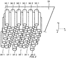
- Fig. 3 is a perspective view of an example of the plurality of cooling pins 94.
- Each cooling pin 94 is shaped as a pillar whose long dimension is in the thickness direction (z-axis direction).
- each cooling pin 94 is shown schematically as a circular pillar, but the shapes of the cooling pins 94 are not limited to this.
- Each cooling pin 94 may instead be shaped as a conical table or polygonal pillar.
- the cooling apparatus 10 includes a plurality of first cooling pins 94-1 and a plurality of second cooling pins 94-2. Each cooling pin 94 is secured to the bottom surface 24 of the top plate 20, in the coolant flow-through portion 92.
- the second cooling pins 94-2 are longer in the thickness direction (z-axis direction) than the first cooling pins 94-1. In other words, the distance between a second cooling pin 94-2 and the top surface 65 of the base plate 64 is less than the distance between a first cooling pin 94-1 and the top surface 65 of the base plate 64. The bottom end of each second cooling pin 94-2 may contact the top surface 65 of the base plate 64.
- the first cooling pins 94-1 may be arranged with a two-dimensional distribution in at least two directions, on the bottom surface 24 of the top plate 20.
- the number of first cooling pins 94-1 arranged per unit area in the xy plane may be uniform across the entire fin region 95, or may be different.
- the first cooling pins 94-1 may be arranged at uniform intervals in a prescribed direction in the xy plane, or may be arranged at non-uniform intervals.
- the first cooling pins 94-1 By providing the first cooling pins 94-1, it is possible to provide a relatively large spatial region between the bottom ends of the cooling pins 94 and the top surface 65 of the base plate 64. Therefore, it becomes easy for foreign matter to pass through this spatial region, and it is possible to prevent the foreign matter from remaining inside the fin region 95. Therefore, it is possible to reduce uneven flow of the coolant caused by the foreign matter, and to reduce the pressure loss occurring when the coolant flows through.
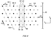
- Fig. 4 shows an example of an arrangement of the first cooling pins 94-1 and the second cooling pins 94-2 in the xy plane. In Fig. 4 , only a portion of the fin region 95 is shown. In Fig. 4 , the first cooling pins 94-1 are shown by white circles and the second cooling pins 94-2 are shown by black circles. The white circles and the black circles are shown at the positions of the cooling pins 94 in the xy plane, and the sizes of the circles do not necessarily match the sizes of the cooling pins 94.
- one or more first cooling pins 94-1 and one or more second cooling pins 94-2 are arranged in an alternating manner, and this pattern appears repeatedly at least twice, in a first direction in the xy plane parallel to the top plate 20.
- one second cooling pin 94-2 and two first cooling pins 94-1 are arranged in an alternating manner, and this pattern appears repeatedly at least twice, in the first direction shown by the straight line 102.
- the first direction in the present example is a direction parallel to the y axis (i.e. a direction parallel to the long edges 28).
- the period with which the second cooling pins 94-2 are arranged in the first direction may be constant across the entire fin region 95, or may be different. In this way, the first cooling pins 94-1 and second cooling pins 94-2 are arranged repeatedly within the fin region 95, and therefore the spatial region that allows foreign matter to flow therethrough can be arranged repeatedly within the fin region 95. Therefore, it is easy to prevent the foreign matter from remaining within the fin region 95.
- first cooling pins 94-1 and one or more second cooling pins 94-2 may be arranged in an alternating manner, and this pattern appears repeatedly at least twice, in a second direction that is different from the first direction.
- the patterns of the first cooling pins 94-1 and second cooling pins 94-2 can be arranged repeating two-dimensionally. Therefore, it is easy to prevent the foreign matter from remaining within the fin region 95.
- one second cooling pin 94-2 and two first cooling pins 94-1 are arranged in an alternating manner, and this pattern appears repeatedly at least twice, in the second direction shown by the straight line 104.
- each cooling pin 94 is arranged at a grid point in a triangular grid, when seen from above, but may instead be arranged at each grid point in a rectangular grid.
- the triangular grid may include a regular triangle grid and an isosceles triangle grid
- the rectangular grid may include a square grid.
- the number of first cooling pins 94-1 provided in the fin region 95 may be greater than the number of second cooling pins 94-2. In this case, the foreign matter can easily pass through. Alternatively, the number of first cooling pins 94-1 provided in the fin region 95 may be less than the number of second cooling pins 94-2. In this case, the total surface area of the cooling pins 94 can be increased. The number of first cooling pins 94-1 provided in the fin region 95 may be the same as the number of second cooling pins 94-2.
- a plurality of first cooling pins 94-1 may be arranged between the second cooling pins 94-2 in at least one of the first direction and the second direction.
- the second cooling pins 94-2 are arranged along the x-axis direction.
- a first cooling pin 94-1 may be arranged between two second cooling pins 94-2 in the x-axis direction, but does not need to be.
- One or more columns 97 of first cooling pins 94-1 are arranged between respective columns 96, oriented in the x-axis direction, of second cooling pins 94-2.
- Second cooling pins 94-2 are not arranged between any two first cooling pins 94-1 in each column 97.
- a spatial region 98 can be provided continuously in a manner to traverse the fin region 95 in a prescribed linear direction.
- the linear direction along which the spatial region 98 is provided is the x-axis direction.
- the spatial region 98 traversing the fin region 95 refers to the spatial region 98 being provided continuously from one end portion of the fin region 95 to another end portion.
- the spatial region 98 is a space in contact with the top surface 65 of the base plate 64.
- the space between the first cooling pins 94-1 and the top surface 65 of the base plate 64 is included in the spatial region 98.
- the spatial region 98 traverses the fin region 95, it becomes even easier to expel foreign matter that has intruded into the fin region 95.
- the spatial region 98 traverses the fin region 95 in the x-axis direction, but as another example, the spatial region 98 may traverse the fin region 95 in a linear direction that is different from the x-axis direction.
- the spatial region 98 preferably traverses the fin region 95 in a manner to connect one coolant flow path 99 with another coolant flow path 99.
- the intervals between cooling pins 94 in the first direction are a first interval P1.
- the intervals between cooling pins 94 in the second direction are a second interval P2.
- the interval between two cooling pins 94 refers to the shortest distance between end portions of the two cooling pins 94.
- the second interval P2 may be the same as the first interval PI, or may be different.
- a third interval between two columns 96 of second cooling pins 94-2 is y1.
- the third interval y1 corresponds to the width of the spatial region 98 in the y-axis direction.
- the distance between the side wall plate 63 and the cooling pin 94 arranged at the end in the longitudinal direction (y-axis direction in the present example) of the top plate 20 and the base plate 64 is y2.
- the distance y2 may be at least double the first interval P1. In this way, it is easy for foreign matter to pass through between the side wall plate 63 and the fin region 95.
- the distance y2 may be at least three times, or at least four times, the first interval P1.
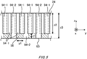
- Fig. 5 is a diagram for describing the spatial region 98.
- the plurality of cooling pins 94 arranged along the y axis are shown by solid lines, and the cooling pins 94 arranged deeper in the x-axis direction than these cooling pins 94 are shown by broken lines.
- the second cooling pins 94-2 are arranged in columns 96 oriented in the x-axis direction.
- First cooling pins 94-1 are arranged between the columns 96. Therefore, the spatial region 98 extending in the x-axis direction is provided between columns 96 of second cooling pins 94-2.
- Fig. 5 diagonal line hatching is shown in the spatial region 98.
- the length of the spatial region 98 in the thickness direction is z1.
- the length z1 corresponds to the distance between the top surface 65 of the base plate 64 and the bottom ends of the first cooling pins 94-1.
- the length z1 is preferably greater than or equal to 1 mm. In this way, the foreign matter can easily pass through.
- the length z1 may be greater than or equal to 2 mm, or greater than or equal to 3 mm.
- a length z2 of each first cooling pin 94-1 may be greater than or equal to half of a distance z3 between the bottom surface 24 of the top plate 20 and the top surface 65 of the base plate 64 (i.e. the thickness of the coolant flow-through portion 92), or may be greater than or equal to 3/4 of the distance z3.
- each cooling pin 94 may have a cross section in the xy plane with an approximately constant pillar shape. Furthermore, at least some of the cooling pins 94 may have a tapered shape in which the cross-sectional area becomes smaller closer to the base plate 64. In this way, it is easy for foreign matter that has intruded into the fin region 95 to move in the direction of the spatial region 98.
- Each first cooling pin 94-1 may have a tapered shape.
- the width y1 of the spatial region 98 in the y-axis direction is preferably greater than or equal to 1 mm. In this way, foreign matter can easily pass through.
- the width y1 may be greater than or equal to 2 mm, or greater than or equal to 3 mm.
- Fig. 6 is a perspective view in which the top plate 20 is shown separated from the case 40.
- the top plate 20 includes a set of opposing short edges 16 and a set of opposing long edges 18 in the xy plane.
- the top plate 20 of the present example has a substantially rectangular shape including the edges 16 and the edges 18.
- the short edges 16 are edges parallel to the x axis
- the long edges 18 are edges parallel to the y axis.
- the top plate 20 is provided with a through-hole 82, which is a portion of a through-hole used to secure the semiconductor module 100 to an external apparatus.
- through-holes 82 are provided at the four corners of the top plate 20, but the number and positions of the through-holes 82 are not limited to this.
- the shape of the top plate 20 is not limited to a rectangular shape such as shown in Fig. 6 .
- the top plate 20 may include portions protruding from each edge in the xy plane.
- the through-holes 82 may be provided in these protruding portions.
- the border portion 62 and the top plate 20 have approximately the same outer shape in the xy plane.
- positions where the top plate 20 and border portion 62 overlap when secured by brazing or the like are shown by dashed lines.
- the cooling pins 94 arranged in the coolant flow-through portion 92 are omitted.
- the brazing material between each member is omitted.
- the border portion 62 is arranged surrounding the coolant flow-through portion 92 and, together with the top plate 20, the side wall plate 63, and the base plate 64, seals the coolant flow-through portion 92.
- the coolant flow-through portion 92 is defined by the bottom surface 24 of the top plate 20 and the top surface 65 and side wall plate 63 of the base plate 64.
- the top plate 20 and the base plate 64 may have the same thickness.
- the border portion 62, the side wall plate 63, and the base plate 64 may be formed by forging a single piece of plate-shaped metal, or may be formed using another method.
- the forging is a method for machining a metal plate into a prescribed shape by performing pressing or compression using a mold or the like with a prescribed shape.
- Fig. 7 is a perspective view of another example of the case 40.
- the top plate 20 and the side wall plate 63 are formed integrally.
- the base plate 64 is secured to the bottom end of the side wall plate 63 by brazing or the like.
- the top plate 20 and the side wall plate 63 may be formed by forging or by another method.
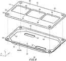
- Fig. 8 is a perspective view of another example of the case 40.
- the case 40 is shown in a state where the top plate 20 has been separated therefrom.
- Fig. 9 is a perspective view of the case 40 in a state where the top plate 20 is secured thereto.
- the top plate 20 has a different structure.
- the other structures are the same as in the case 40 described in any of Figs. 1 to 7 .
- the top plate 20 of the present example includes one or more recessed portions 30 in the top surface 22.
- the thickness of the recessed portion 30 in the thickness direction of the top plate 20 is less than the thickness of the top plate 20 in regions other than the recessed portion 30. It should be noted that the recessed portion 30 does not penetrate entirely through the top plate 20.
- a peripheral portion 32 that surrounds the recessed portion 30 is provided on the top plate 20.
- the peripheral portion 32 may be provided with a ring shape along the edges 16 and 18 of the top plate 20.
- the thickness of the top plate 20 in the z-axis direction at the peripheral portion 32 is greater than the thickness of the top plate 20 in the z-axis direction in at the recessed portion 30.
- the circuit substrate 76, the semiconductor chip 78, and the like shown in Fig. 1 are arranged in the recessed portion 30. Furthermore, the recessed portion 30 is arranged in at least part of a region overlapping with the first cooling pins 94-1 or the second cooling pins 94-2 (i.e. the fin region 95).
- the recessed portion 30 overlapping with the fin region 95 refers to at least a partial region of the recessed portion 30 overlapping with the fin region 95 when the recessed portion 30 and the fin region 95 are projected onto the same xy plane.
- the entire region of the recessed portion 30 is preferably arranged overlapping with the fin region 95.
- Both the first cooling pins 94-1 and the second cooling pins 94-2 are preferably arranged in a region overlapping with the recessed portion 30.
- the recessed portion 30 By providing the recessed portion 30, it is possible to reduce the thickness of the top plate 20 between the circuit substrate 76 and the cooling pins 94, and to efficiently transfer the heat generated by the semiconductor device 70 to the cooling pin 94. Furthermore, by increasing the thickness of the top plate 20 at the peripheral portion 32 surrounding the recessed portion 30, it is possible to maintain the mechanical strength of the top plate 20. In this way, deformation of the top plate 20 can be restricted.
- the top plate 20 includes a plurality of the recessed portions 30, an intermediate region 34 is provided between two recessed portions 30.
- the intermediate region 34 is a region between the circuit substrates 76 arranged respectively in the recessed portions 30.
- a plurality of recessed portions 30 are arranged in the y-axis direction in the top surface 22 of the top plate 20 of the present example.
- the recessed portions 30 may be arranged to overlap with the center of the top surface 22 of the top plate 20 in the x-axis direction.
- the center position of the recessed portion 30 in the x-axis direction may match the center position of the top surface 22.
- the thickness of the top plate 20 at the intermediate region 34 is greater than the thickness of the top plate 20 at the recessed portion 30.
- the thickness of the top plate 20 at the intermediate region 34 may be the same as the thickness of the top plate 20 at the peripheral portion 32.
- the top plate 20 may be a single continuous plate member. In this case, the recessed portion 30 may be formed by forging.
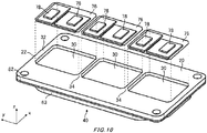
- Fig. 10 is a perspective view of an example of the circuit substrate 76 and the semiconductor chip 78 arranged in the recessed portion 30.
- Each recessed portion 30 has one or more circuit substrates 76 arranged therein.
- one circuit substrate 76 is arranged in each recessed portion 30.
- the shape of the recessed portion 30 in the xy plane may be the same as the shape of the circuit substrate 76 in the xy plane.
- a lead frame and the like connected to the circuit substrate 76 and the semiconductor chip 78 is omitted from Fig. 10 .
- Each circuit substrate 76 is provided with one or more semiconductor chips 78.
- circuit substrates 76 and semiconductor chips 78 used in a three-phase inverter are arranged on the top surface 22 of the top plate 20.
- a circuit substrate 76 and semiconductor chips 78 for a single phase are arranged in each recessed portion 30.
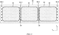
- Fig. 11 shows an example of an arrangement of recessed portions 30 and the fin region 95.
- the recessed portions 30 and the fin region 95 are projected onto the same xy plane.
- the recessed portions 30 are shown by solid lines, and the cooling pins 94 are shown by circles formed of broken lines.
- both first cooling pins 94-1 and second cooling pins 94-2 may be arranged at least in the region overlapping with the recessed portions 30. In this way, it is possible to prevent the accumulation of foreign matter between the cooling pins 94 below the circuit substrates 76. Furthermore, both first cooling pins 94-1 and second cooling pins 94-2 may be arranged at least in the region overlapping with the semiconductor chips 78.
- Third cooling pins 94-3 may be arranged at positions overlapping with the intermediate region 34.
- the third cooling pins 94-3 are shows by black circles. It is acceptable for only the third cooling pins 94-3 to be arranged at the positions overlapping with the intermediate region 34, or at least one of first cooling pins 94-1 and second cooling pins 94-2 may be arranged in addition to the third cooling pins 94-3 at the positions overlapping with the intermediate region 34. In the present example, the third cooling pins 94-3 are not arranged in the region overlapping with the recessed portion 30.
- each third cooling pin 94-3 in the z-axis direction may be less than or equal to half the thickness of the coolant flow-through portion 92.
- the third cooling pins 94-3 it is possible for foreign matter to pass through even more easily.
- the third cooling pins 94-3 are not arranged in the region overlapping with the recessed portions 30, it is possible to reduce a decrease in the heat dispersion capability caused by the shortening of the cooling pins 94.
- the third cooling pins 94-3 may be provided in regions between two circuit substrates 76.
- the third cooling pins 94-3 may also be arranged in the region between the side wall plate 63 and the recessed portions 30, in the y-axis direction. In this way, foreign matter can easily pass through the region contacting the side wall plate 63. Yet further, although not shown in Fig. 11 , the third cooling pins 94-3 may also be arranged in the region between the side wall plate 63 and the recessed portions 30, in the x-axis direction as well. As an example, cooling pins 94 that do not overlap with the recessed portions 30 may all be third cooling pins 94-3. The arrangement of the cooling pins 94 that are not third cooling pins 94-3 is the same as the arrangement described in Fig. 4 .
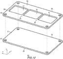
- Fig. 12 is a perspective view of an example of the structure of the top plate 20 including the recessed portions 30.
- the top plate 20 of the present example may be applied to any of the embodiments described in Figs. 1 to 11 .
- the top plate 20 of the present example includes a lower plate-shaped portion 23 and an upper frame-shaped portion 25.
- the lower plate-shaped portion 23 is shaped as a plate including a top surface 27 and a bottom surface 29.
- a plurality of cooling pins 94 including first cooling pins 94-1 and second cooling pins 94-2, are secured to the bottom surface 29.
- the lower plate-shaped portion 23 is provided with a through-hole 81 that becomes a portion of the through-hole 82.
- the upper frame-shaped portion 25 is secured to the top surface 27 of the lower plate-shaped portion 23 by brazing or the like.
- the upper frame-shaped portion 25 is a frame-shaped member provided with a penetration opening 31 in a region corresponding to the recessed portion 30.
- the shape of the penetration opening 31 is the same as the shape of the recessed portion 30.
- the upper frame-shaped portion 25 includes a peripheral portion 33 arranged surrounding the penetration opening 31.
- the peripheral portion 33 is provided in a region corresponding to the peripheral portion 32 described in Fig. 8 .
- the upper frame-shaped portion 25 includes an intermediate portion 35 between two penetration openings 31.
- the intermediate portion 35 is provided in the region corresponding to the intermediate region 34 described in Fig. 8 .
- a through-hole 83 that becomes a portion of the through-hole 82 is provided in the upper frame-shaped portion 25. Due to the structure in which the lower plate-shaped portion 23 and the upper frame-shaped portion 25 are provided, it is possible to form the top plate 20 including the recessed portion 30 with a simple process.
- Fig. 13 shows an overview of a vehicle 200 according to one embodiment of the present invention.
- the vehicle 200 is a vehicle that generates at least some of its thrust using electrical power.
- the vehicle 200 may be an electric automobile in which all of the thrust is generated by a power-driven device such as a motor, or may be a hybrid vehicle that uses both a power-driven device such as a motor and an internal combustion engine that is driven by fuel such as gasoline.
- the vehicle 200 includes a control apparatus 210 (external apparatus) that controls the power-driven device such as the motor.
- the control apparatus 210 is provided with the semiconductor module 100.
- the semiconductor module 100 may control the power supplied to the power-driven device.
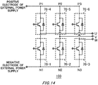
- Fig. 14 is a main circuit diagram of the semiconductor module 100 according to one embodiment of the present invention.
- the semiconductor module 100 may be part of an in-vehicle unit that drives a motor of a vehicle.
- the semiconductor module 100 may function as a three-phase AC inverter circuit that includes output terminals U, V, and W.
- a plurality of semiconductor chips 78-1, 78-2, and 78-3 may form a lower arm in the semiconductor module 100, and a plurality of semiconductor chips 78-4, 78-5, and 78-6 may form an upper arm in the semiconductor module 100.
- One set of semiconductor chips 78-1 and 78-4 may form a leg.
- One set of semiconductor chips 78-2 and 78-5 and one set of semiconductor chips 78-3 and 78-6 may each form a leg in the same manner.
- the semiconductor chips 78 are arranged in the recessed portions 30 described above, in leg units.
- the emitter electrode may be electrically connected to an input terminal N1, and the collector electrode may be connected to the output terminal U.
- the emitter electrode may be electrically connected to the output terminal U, and the collector electrode may be electrically connected to an input terminal P1.
- the emitter terminals may be electrically connected to input terminals N2 and N3, respectively, and the collector terminals may be electrically connected to the output terminals V and W, respectively.
- the emitter terminals may be electrically connected to the output terminals V and W, respectively, and the collector terminals may be electrically connected to input terminals P2 and P3, respectively.
- Each semiconductor chip 78-1 to 78-6 may be switched alternately by a signal input to the control electrode pad of the semiconductor chip 78.
- each semiconductor chip 78 may generate heat when switching.
- the input terminals PI, P2, and P3 may be connected to a positive electrode of an external power supply, the input terminals N1, N2, and N3 may be connected to a negative electrode of the external power supply, and the output terminals U, V, and W may be connected to a load.
- the input terminals PI, P2, and P3 may be electrically connected to each other, and the other input terminals N1, N2, and N3 may be electrically connected to each other.
- the plurality of semiconductor chips 78-1 to 78-6 may each be an RC-IGBT (reverse-conducting IGBT) semiconductor chip.
- the IGBT and the freewheel diode (FWD) are formed integrally, and the IGBT and FWD may be connected in antiparallel.
- the plurality of semiconductor chips 78-1 to 78-6 may each include a combination of a transistor, such as a MOSFET or IGBT, and a diode.
- the chip substrate of the transistor and the diode may be a silicon substrate, a silicon carbide substrate, or a gallium nitride substrate.
Landscapes
- Engineering & Computer Science (AREA)
- Microelectronics & Electronic Packaging (AREA)
- Physics & Mathematics (AREA)
- Thermal Sciences (AREA)
- Cooling Or The Like Of Semiconductors Or Solid State Devices (AREA)
- Arrangement Or Mounting Of Propulsion Units For Vehicles (AREA)
- Cooling, Air Intake And Gas Exhaust, And Fuel Tank Arrangements In Propulsion Units (AREA)
- Cooling Or The Like Of Electrical Apparatus (AREA)
Applications Claiming Priority (1)
| Application Number | Priority Date | Filing Date | Title |
|---|---|---|---|
| JP2018100796A JP7159617B2 (ja) | 2018-05-25 | 2018-05-25 | 冷却装置、半導体モジュール、車両および製造方法 |
Publications (2)
| Publication Number | Publication Date |
|---|---|
| EP3573097A1 true EP3573097A1 (de) | 2019-11-27 |
| EP3573097B1 EP3573097B1 (de) | 2021-12-15 |
Family
ID=66286111
Family Applications (1)
| Application Number | Title | Priority Date | Filing Date |
|---|---|---|---|
| EP19170897.3A Active EP3573097B1 (de) | 2018-05-25 | 2019-04-24 | Kühlvorrichtung, halbleitermodul, fahrzeug und herstellungsverfahren |
Country Status (4)
| Country | Link |
|---|---|
| US (1) | US11011453B2 (de) |
| EP (1) | EP3573097B1 (de) |
| JP (1) | JP7159617B2 (de) |
| CN (1) | CN110534486B (de) |
Families Citing this family (17)
| Publication number | Priority date | Publication date | Assignee | Title |
|---|---|---|---|---|
| KR102554431B1 (ko) * | 2018-09-05 | 2023-07-13 | 삼성전자주식회사 | 반도체 장치 및 반도체 장치 제조 방법 |
| JP7205662B2 (ja) * | 2020-03-18 | 2023-01-17 | 富士電機株式会社 | 半導体モジュール |
| JP7487533B2 (ja) * | 2020-04-02 | 2024-05-21 | 富士電機株式会社 | 半導体モジュールおよび車両 |
| JP7463825B2 (ja) * | 2020-04-27 | 2024-04-09 | 富士電機株式会社 | 半導体モジュールおよび車両 |
| DE102020112082B3 (de) * | 2020-05-05 | 2021-06-10 | Semikron Elektronik Gmbh & Co. Kg | Leistungshalbleitereinrichtung mit Leistungshalbleiterschaltern und mit einem Gehäuse |
| WO2021256083A1 (ja) | 2020-06-17 | 2021-12-23 | 富士電機株式会社 | 冷却装置および半導体モジュール |
| JP7577948B2 (ja) * | 2020-09-15 | 2024-11-06 | 富士電機株式会社 | 冷却器及び半導体装置 |
| DE102020132689B4 (de) * | 2020-12-08 | 2022-06-30 | Semikron Elektronik Gmbh & Co. Kg | Leistungselektronisches System mit einer Schalteinrichtung und mit einer Flüssigkeitskühleinrichtung |
| KR102308872B1 (ko) | 2021-02-02 | 2021-10-05 | 제엠제코(주) | 반도체 부품 쿨링 시스템, 반도체 부품 쿨링 시스템 제조방법, 및 반도체 부품 쿨링 시스템이 적용된 반도체 패키지 |
| JP6984778B1 (ja) * | 2021-05-20 | 2021-12-22 | 富士電機株式会社 | 冷却装置および冷却装置を備える半導体装置 |
| DE102021214226A1 (de) * | 2021-12-13 | 2023-06-15 | Robert Bosch Gesellschaft mit beschränkter Haftung | Kühlkörper zur Kühlung einer elektrischen und/oder elektronischen Baugruppe |
| US20240175645A1 (en) * | 2022-11-30 | 2024-05-30 | Valeo Systemes Thermiques | Attachment for a heat exchanger |
| FR3149373B1 (fr) * | 2023-06-01 | 2025-05-16 | Valeo Eautomotive Germany Gmbh | Structure de refroidissement, convertisseur de puissance électrique comprenant une telle structure de refroidissement et véhicule |
| JP2025098799A (ja) * | 2023-12-20 | 2025-07-02 | Astemo株式会社 | 電力変換装置の製造方法、電力変換装置 |
| US20260020185A1 (en) * | 2024-07-10 | 2026-01-15 | Amulaire Thermal Technology, Inc. | Liquid-cooling cooler for power module of electric vehicle |
| CN119764271B (zh) * | 2024-12-11 | 2025-11-04 | 北京国家新能源汽车技术创新中心有限公司 | 冷却油直流汇聚式功率模块浸没散热结构 |
| CN121262807A (zh) * | 2025-12-04 | 2026-01-02 | 广州众山新材料股份有限公司 | 散热基板及其加工方法和液冷板 |
Citations (7)
| Publication number | Priority date | Publication date | Assignee | Title |
|---|---|---|---|---|
| JPS6239997B2 (de) | 1977-07-16 | 1987-08-26 | Roehm Gmbh | |
| JP2003008264A (ja) * | 2001-06-26 | 2003-01-10 | Nissan Motor Co Ltd | 電子部品の冷却装置 |
| US20100172104A1 (en) * | 2009-01-08 | 2010-07-08 | Toyota Jidosha Kabushiki Kaisha | Heat dissipation device and power module |
| JP2015015274A (ja) | 2013-07-03 | 2015-01-22 | 三菱電機株式会社 | 電力用半導体装置 |
| DE112014000898T5 (de) * | 2013-09-05 | 2015-11-26 | Fuji Electric Co., Ltd. | Leistungshalbleitermodul |
| JP2016225530A (ja) | 2015-06-02 | 2016-12-28 | 昭和電工株式会社 | 液冷式冷却装置 |
| JP2017017133A (ja) * | 2015-06-30 | 2017-01-19 | 昭和電工株式会社 | 液冷式冷却装置 |
Family Cites Families (13)
| Publication number | Priority date | Publication date | Assignee | Title |
|---|---|---|---|---|
| JP2658427B2 (ja) * | 1989-01-17 | 1997-09-30 | 富士電機株式会社 | 電力変換用半導体素子のスナバ回路とそのモジュール装置 |
| US6729383B1 (en) * | 1999-12-16 | 2004-05-04 | The United States Of America As Represented By The Secretary Of The Navy | Fluid-cooled heat sink with turbulence-enhancing support pins |
| JP2003324173A (ja) * | 2002-05-02 | 2003-11-14 | Nissan Motor Co Ltd | 半導体素子の冷却装置 |
| JP2005191502A (ja) | 2003-12-26 | 2005-07-14 | Nichicon Corp | 電子部品冷却装置 |
| JP2008098432A (ja) * | 2006-10-12 | 2008-04-24 | Fujitsu Ltd | 電子部品の放熱装置 |
| JP2011091301A (ja) * | 2009-10-26 | 2011-05-06 | Toyota Industries Corp | 液冷式冷却装置 |
| JP2011155207A (ja) | 2010-01-28 | 2011-08-11 | Aisin Aw Co Ltd | インバータモジュールの製造方法及びインバータモジュール |
| JP5287919B2 (ja) | 2011-04-01 | 2013-09-11 | トヨタ自動車株式会社 | ヒートシンク、およびヒートシンク付き電子部品 |
| JP5901343B2 (ja) * | 2012-02-24 | 2016-04-06 | 三菱電機株式会社 | 冷却器及び冷却装置 |
| JP6239997B2 (ja) | 2014-02-19 | 2017-11-29 | 株式会社Uacj | 冷却器 |
| CN105531819B (zh) * | 2014-03-14 | 2018-05-08 | 富士电机株式会社 | 冷却器及具有该冷却器的半导体装置 |
| JP6360722B2 (ja) * | 2014-05-30 | 2018-07-18 | Dowaメタルテック株式会社 | くし歯形放熱ピン部材を用いたパワー半導体の水冷用ピン付き放熱板 |
| JP2016105441A (ja) | 2014-12-01 | 2016-06-09 | トヨタ自動車株式会社 | 電力変換器 |
-
2018
- 2018-05-25 JP JP2018100796A patent/JP7159617B2/ja active Active
-
2019
- 2019-04-19 CN CN201910317888.4A patent/CN110534486B/zh active Active
- 2019-04-22 US US16/390,005 patent/US11011453B2/en active Active
- 2019-04-24 EP EP19170897.3A patent/EP3573097B1/de active Active
Patent Citations (7)
| Publication number | Priority date | Publication date | Assignee | Title |
|---|---|---|---|---|
| JPS6239997B2 (de) | 1977-07-16 | 1987-08-26 | Roehm Gmbh | |
| JP2003008264A (ja) * | 2001-06-26 | 2003-01-10 | Nissan Motor Co Ltd | 電子部品の冷却装置 |
| US20100172104A1 (en) * | 2009-01-08 | 2010-07-08 | Toyota Jidosha Kabushiki Kaisha | Heat dissipation device and power module |
| JP2015015274A (ja) | 2013-07-03 | 2015-01-22 | 三菱電機株式会社 | 電力用半導体装置 |
| DE112014000898T5 (de) * | 2013-09-05 | 2015-11-26 | Fuji Electric Co., Ltd. | Leistungshalbleitermodul |
| JP2016225530A (ja) | 2015-06-02 | 2016-12-28 | 昭和電工株式会社 | 液冷式冷却装置 |
| JP2017017133A (ja) * | 2015-06-30 | 2017-01-19 | 昭和電工株式会社 | 液冷式冷却装置 |
Also Published As
| Publication number | Publication date |
|---|---|
| CN110534486B (zh) | 2025-02-25 |
| US11011453B2 (en) | 2021-05-18 |
| JP2019204922A (ja) | 2019-11-28 |
| US20190363036A1 (en) | 2019-11-28 |
| CN110534486A (zh) | 2019-12-03 |
| EP3573097B1 (de) | 2021-12-15 |
| JP7159617B2 (ja) | 2022-10-25 |
Similar Documents
| Publication | Publication Date | Title |
|---|---|---|
| US11011453B2 (en) | Cooling apparatus, semiconductor module, vehicle, and manufacturing method | |
| US11538736B2 (en) | Cooling apparatus, semiconductor module, and vehicle | |
| US20200170147A1 (en) | Semiconductor module, vehicle and manufacturing method | |
| US11251108B2 (en) | Semiconductor module mounted on a cooling device for use in a vehicle | |
| JP7367394B2 (ja) | 半導体モジュール、車両および製造方法 | |
| JP7400896B2 (ja) | 半導体モジュール | |
| US11908772B2 (en) | Semiconductor module and vehicle | |
| JP2020136366A (ja) | 半導体モジュール、車両および製造方法 | |
| JP7666700B2 (ja) | 半導体モジュールおよび車両 | |
| JP2019186237A (ja) | 冷却装置、半導体モジュールおよび車両 | |
| US12127382B2 (en) | Semiconductor module with cooling fins in a matrix form | |
| CN114747003A (zh) | 冷却装置和半导体模块 | |
| CN112509993B (zh) | 半导体模块及车辆 | |
| WO2024262175A1 (ja) | 冷却器、半導体装置、及び車両 |
Legal Events
| Date | Code | Title | Description |
|---|---|---|---|
| PUAI | Public reference made under article 153(3) epc to a published international application that has entered the european phase |
Free format text: ORIGINAL CODE: 0009012 |
|
| STAA | Information on the status of an ep patent application or granted ep patent |
Free format text: STATUS: THE APPLICATION HAS BEEN PUBLISHED |
|
| AK | Designated contracting states |
Kind code of ref document: A1 Designated state(s): AL AT BE BG CH CY CZ DE DK EE ES FI FR GB GR HR HU IE IS IT LI LT LU LV MC MK MT NL NO PL PT RO RS SE SI SK SM TR |
|
| AX | Request for extension of the european patent |
Extension state: BA ME |
|
| STAA | Information on the status of an ep patent application or granted ep patent |
Free format text: STATUS: REQUEST FOR EXAMINATION WAS MADE |
|
| 17P | Request for examination filed |
Effective date: 20200525 |
|
| RBV | Designated contracting states (corrected) |
Designated state(s): AL AT BE BG CH CY CZ DE DK EE ES FI FR GB GR HR HU IE IS IT LI LT LU LV MC MK MT NL NO PL PT RO RS SE SI SK SM TR |
|
| STAA | Information on the status of an ep patent application or granted ep patent |
Free format text: STATUS: EXAMINATION IS IN PROGRESS |
|
| 17Q | First examination report despatched |
Effective date: 20201109 |
|
| RIC1 | Information provided on ipc code assigned before grant |
Ipc: H01L 23/473 20060101AFI20210520BHEP Ipc: H05K 7/20 20060101ALI20210520BHEP Ipc: H01L 23/367 20060101ALN20210520BHEP Ipc: H01L 23/467 20060101ALN20210520BHEP |
|
| GRAP | Despatch of communication of intention to grant a patent |
Free format text: ORIGINAL CODE: EPIDOSNIGR1 |
|
| STAA | Information on the status of an ep patent application or granted ep patent |
Free format text: STATUS: GRANT OF PATENT IS INTENDED |
|
| INTG | Intention to grant announced |
Effective date: 20210625 |
|
| GRAS | Grant fee paid |
Free format text: ORIGINAL CODE: EPIDOSNIGR3 |
|
| GRAA | (expected) grant |
Free format text: ORIGINAL CODE: 0009210 |
|
| STAA | Information on the status of an ep patent application or granted ep patent |
Free format text: STATUS: THE PATENT HAS BEEN GRANTED |
|
| AK | Designated contracting states |
Kind code of ref document: B1 Designated state(s): AL AT BE BG CH CY CZ DE DK EE ES FI FR GB GR HR HU IE IS IT LI LT LU LV MC MK MT NL NO PL PT RO RS SE SI SK SM TR |
|
| REG | Reference to a national code |
Ref country code: GB Ref legal event code: FG4D Ref country code: CH Ref legal event code: EP |
|
| REG | Reference to a national code |
Ref country code: IE Ref legal event code: FG4D Ref country code: DE Ref legal event code: R096 Ref document number: 602019010008 Country of ref document: DE |
|
| REG | Reference to a national code |
Ref country code: AT Ref legal event code: REF Ref document number: 1456130 Country of ref document: AT Kind code of ref document: T Effective date: 20220115 |
|
| REG | Reference to a national code |
Ref country code: LT Ref legal event code: MG9D |
|
| REG | Reference to a national code |
Ref country code: NL Ref legal event code: MP Effective date: 20211215 |
|
| PG25 | Lapsed in a contracting state [announced via postgrant information from national office to epo] |
Ref country code: RS Free format text: LAPSE BECAUSE OF FAILURE TO SUBMIT A TRANSLATION OF THE DESCRIPTION OR TO PAY THE FEE WITHIN THE PRESCRIBED TIME-LIMIT Effective date: 20211215 Ref country code: LT Free format text: LAPSE BECAUSE OF FAILURE TO SUBMIT A TRANSLATION OF THE DESCRIPTION OR TO PAY THE FEE WITHIN THE PRESCRIBED TIME-LIMIT Effective date: 20211215 Ref country code: FI Free format text: LAPSE BECAUSE OF FAILURE TO SUBMIT A TRANSLATION OF THE DESCRIPTION OR TO PAY THE FEE WITHIN THE PRESCRIBED TIME-LIMIT Effective date: 20211215 Ref country code: BG Free format text: LAPSE BECAUSE OF FAILURE TO SUBMIT A TRANSLATION OF THE DESCRIPTION OR TO PAY THE FEE WITHIN THE PRESCRIBED TIME-LIMIT Effective date: 20220315 |
|
| REG | Reference to a national code |
Ref country code: AT Ref legal event code: MK05 Ref document number: 1456130 Country of ref document: AT Kind code of ref document: T Effective date: 20211215 |
|
| PG25 | Lapsed in a contracting state [announced via postgrant information from national office to epo] |
Ref country code: SE Free format text: LAPSE BECAUSE OF FAILURE TO SUBMIT A TRANSLATION OF THE DESCRIPTION OR TO PAY THE FEE WITHIN THE PRESCRIBED TIME-LIMIT Effective date: 20211215 Ref country code: NO Free format text: LAPSE BECAUSE OF FAILURE TO SUBMIT A TRANSLATION OF THE DESCRIPTION OR TO PAY THE FEE WITHIN THE PRESCRIBED TIME-LIMIT Effective date: 20220315 Ref country code: LV Free format text: LAPSE BECAUSE OF FAILURE TO SUBMIT A TRANSLATION OF THE DESCRIPTION OR TO PAY THE FEE WITHIN THE PRESCRIBED TIME-LIMIT Effective date: 20211215 Ref country code: HR Free format text: LAPSE BECAUSE OF FAILURE TO SUBMIT A TRANSLATION OF THE DESCRIPTION OR TO PAY THE FEE WITHIN THE PRESCRIBED TIME-LIMIT Effective date: 20211215 Ref country code: GR Free format text: LAPSE BECAUSE OF FAILURE TO SUBMIT A TRANSLATION OF THE DESCRIPTION OR TO PAY THE FEE WITHIN THE PRESCRIBED TIME-LIMIT Effective date: 20220316 |
|
| PG25 | Lapsed in a contracting state [announced via postgrant information from national office to epo] |
Ref country code: NL Free format text: LAPSE BECAUSE OF FAILURE TO SUBMIT A TRANSLATION OF THE DESCRIPTION OR TO PAY THE FEE WITHIN THE PRESCRIBED TIME-LIMIT Effective date: 20211215 |
|
| PG25 | Lapsed in a contracting state [announced via postgrant information from national office to epo] |
Ref country code: SM Free format text: LAPSE BECAUSE OF FAILURE TO SUBMIT A TRANSLATION OF THE DESCRIPTION OR TO PAY THE FEE WITHIN THE PRESCRIBED TIME-LIMIT Effective date: 20211215 Ref country code: SK Free format text: LAPSE BECAUSE OF FAILURE TO SUBMIT A TRANSLATION OF THE DESCRIPTION OR TO PAY THE FEE WITHIN THE PRESCRIBED TIME-LIMIT Effective date: 20211215 Ref country code: RO Free format text: LAPSE BECAUSE OF FAILURE TO SUBMIT A TRANSLATION OF THE DESCRIPTION OR TO PAY THE FEE WITHIN THE PRESCRIBED TIME-LIMIT Effective date: 20211215 Ref country code: PT Free format text: LAPSE BECAUSE OF FAILURE TO SUBMIT A TRANSLATION OF THE DESCRIPTION OR TO PAY THE FEE WITHIN THE PRESCRIBED TIME-LIMIT Effective date: 20220418 Ref country code: ES Free format text: LAPSE BECAUSE OF FAILURE TO SUBMIT A TRANSLATION OF THE DESCRIPTION OR TO PAY THE FEE WITHIN THE PRESCRIBED TIME-LIMIT Effective date: 20211215 Ref country code: EE Free format text: LAPSE BECAUSE OF FAILURE TO SUBMIT A TRANSLATION OF THE DESCRIPTION OR TO PAY THE FEE WITHIN THE PRESCRIBED TIME-LIMIT Effective date: 20211215 Ref country code: CZ Free format text: LAPSE BECAUSE OF FAILURE TO SUBMIT A TRANSLATION OF THE DESCRIPTION OR TO PAY THE FEE WITHIN THE PRESCRIBED TIME-LIMIT Effective date: 20211215 |
|
| PG25 | Lapsed in a contracting state [announced via postgrant information from national office to epo] |
Ref country code: PL Free format text: LAPSE BECAUSE OF FAILURE TO SUBMIT A TRANSLATION OF THE DESCRIPTION OR TO PAY THE FEE WITHIN THE PRESCRIBED TIME-LIMIT Effective date: 20211215 Ref country code: AT Free format text: LAPSE BECAUSE OF FAILURE TO SUBMIT A TRANSLATION OF THE DESCRIPTION OR TO PAY THE FEE WITHIN THE PRESCRIBED TIME-LIMIT Effective date: 20211215 |
|
| REG | Reference to a national code |
Ref country code: DE Ref legal event code: R097 Ref document number: 602019010008 Country of ref document: DE |
|
| PG25 | Lapsed in a contracting state [announced via postgrant information from national office to epo] |
Ref country code: IS Free format text: LAPSE BECAUSE OF FAILURE TO SUBMIT A TRANSLATION OF THE DESCRIPTION OR TO PAY THE FEE WITHIN THE PRESCRIBED TIME-LIMIT Effective date: 20220415 |
|
| PLBE | No opposition filed within time limit |
Free format text: ORIGINAL CODE: 0009261 |
|
| STAA | Information on the status of an ep patent application or granted ep patent |
Free format text: STATUS: NO OPPOSITION FILED WITHIN TIME LIMIT |
|
| PG25 | Lapsed in a contracting state [announced via postgrant information from national office to epo] |
Ref country code: DK Free format text: LAPSE BECAUSE OF FAILURE TO SUBMIT A TRANSLATION OF THE DESCRIPTION OR TO PAY THE FEE WITHIN THE PRESCRIBED TIME-LIMIT Effective date: 20211215 Ref country code: AL Free format text: LAPSE BECAUSE OF FAILURE TO SUBMIT A TRANSLATION OF THE DESCRIPTION OR TO PAY THE FEE WITHIN THE PRESCRIBED TIME-LIMIT Effective date: 20211215 |
|
| 26N | No opposition filed |
Effective date: 20220916 |
|
| PG25 | Lapsed in a contracting state [announced via postgrant information from national office to epo] |
Ref country code: SI Free format text: LAPSE BECAUSE OF FAILURE TO SUBMIT A TRANSLATION OF THE DESCRIPTION OR TO PAY THE FEE WITHIN THE PRESCRIBED TIME-LIMIT Effective date: 20211215 |
|
| REG | Reference to a national code |
Ref country code: CH Ref legal event code: PL |
|
| REG | Reference to a national code |
Ref country code: BE Ref legal event code: MM Effective date: 20220430 |
|
| PG25 | Lapsed in a contracting state [announced via postgrant information from national office to epo] |
Ref country code: MC Free format text: LAPSE BECAUSE OF FAILURE TO SUBMIT A TRANSLATION OF THE DESCRIPTION OR TO PAY THE FEE WITHIN THE PRESCRIBED TIME-LIMIT Effective date: 20211215 Ref country code: LU Free format text: LAPSE BECAUSE OF NON-PAYMENT OF DUE FEES Effective date: 20220424 Ref country code: LI Free format text: LAPSE BECAUSE OF NON-PAYMENT OF DUE FEES Effective date: 20220430 Ref country code: CH Free format text: LAPSE BECAUSE OF NON-PAYMENT OF DUE FEES Effective date: 20220430 |
|
| PG25 | Lapsed in a contracting state [announced via postgrant information from national office to epo] |
Ref country code: BE Free format text: LAPSE BECAUSE OF NON-PAYMENT OF DUE FEES Effective date: 20220430 |
|
| PG25 | Lapsed in a contracting state [announced via postgrant information from national office to epo] |
Ref country code: IE Free format text: LAPSE BECAUSE OF NON-PAYMENT OF DUE FEES Effective date: 20220424 |
|
| PG25 | Lapsed in a contracting state [announced via postgrant information from national office to epo] |
Ref country code: IT Free format text: LAPSE BECAUSE OF FAILURE TO SUBMIT A TRANSLATION OF THE DESCRIPTION OR TO PAY THE FEE WITHIN THE PRESCRIBED TIME-LIMIT Effective date: 20211215 |
|
| GBPC | Gb: european patent ceased through non-payment of renewal fee |
Effective date: 20230424 |
|
| PG25 | Lapsed in a contracting state [announced via postgrant information from national office to epo] |
Ref country code: GB Free format text: LAPSE BECAUSE OF NON-PAYMENT OF DUE FEES Effective date: 20230424 |
|
| PG25 | Lapsed in a contracting state [announced via postgrant information from national office to epo] |
Ref country code: GB Free format text: LAPSE BECAUSE OF NON-PAYMENT OF DUE FEES Effective date: 20230424 |
|
| PG25 | Lapsed in a contracting state [announced via postgrant information from national office to epo] |
Ref country code: HU Free format text: LAPSE BECAUSE OF FAILURE TO SUBMIT A TRANSLATION OF THE DESCRIPTION OR TO PAY THE FEE WITHIN THE PRESCRIBED TIME-LIMIT; INVALID AB INITIO Effective date: 20190424 |
|
| PG25 | Lapsed in a contracting state [announced via postgrant information from national office to epo] |
Ref country code: MK Free format text: LAPSE BECAUSE OF FAILURE TO SUBMIT A TRANSLATION OF THE DESCRIPTION OR TO PAY THE FEE WITHIN THE PRESCRIBED TIME-LIMIT Effective date: 20211215 Ref country code: CY Free format text: LAPSE BECAUSE OF FAILURE TO SUBMIT A TRANSLATION OF THE DESCRIPTION OR TO PAY THE FEE WITHIN THE PRESCRIBED TIME-LIMIT Effective date: 20211215 |
|
| PG25 | Lapsed in a contracting state [announced via postgrant information from national office to epo] |
Ref country code: MT Free format text: LAPSE BECAUSE OF FAILURE TO SUBMIT A TRANSLATION OF THE DESCRIPTION OR TO PAY THE FEE WITHIN THE PRESCRIBED TIME-LIMIT Effective date: 20211215 |
|
| REG | Reference to a national code |
Ref country code: DE Ref legal event code: R079 Ref document number: 602019010008 Country of ref document: DE Free format text: PREVIOUS MAIN CLASS: H01L0023473000 Ipc: H10W0040470000 |
|
| PG25 | Lapsed in a contracting state [announced via postgrant information from national office to epo] |
Ref country code: TR Free format text: LAPSE BECAUSE OF FAILURE TO SUBMIT A TRANSLATION OF THE DESCRIPTION OR TO PAY THE FEE WITHIN THE PRESCRIBED TIME-LIMIT Effective date: 20211215 |
|
| PGFP | Annual fee paid to national office [announced via postgrant information from national office to epo] |
Ref country code: FR Payment date: 20260309 Year of fee payment: 8 |
|
| PGFP | Annual fee paid to national office [announced via postgrant information from national office to epo] |
Ref country code: DE Payment date: 20260305 Year of fee payment: 8 |