EP3573242A1 - Générateur de fréquence et procédé de génération de fréquence - Google Patents
Générateur de fréquence et procédé de génération de fréquence Download PDFInfo
- Publication number
- EP3573242A1 EP3573242A1 EP18897872.0A EP18897872A EP3573242A1 EP 3573242 A1 EP3573242 A1 EP 3573242A1 EP 18897872 A EP18897872 A EP 18897872A EP 3573242 A1 EP3573242 A1 EP 3573242A1
- Authority
- EP
- European Patent Office
- Prior art keywords
- signal
- frequency
- generate
- phase
- circulating
- Prior art date
- Legal status (The legal status is an assumption and is not a legal conclusion. Google has not performed a legal analysis and makes no representation as to the accuracy of the status listed.)
- Granted
Links
Images



Classifications
-
- H—ELECTRICITY
- H03—ELECTRONIC CIRCUITRY
- H03K—PULSE TECHNIQUE
- H03K19/00—Logic circuits, i.e. having at least two inputs acting on one output; Inverting circuits
- H03K19/02—Logic circuits, i.e. having at least two inputs acting on one output; Inverting circuits using specified components
- H03K19/16—Logic circuits, i.e. having at least two inputs acting on one output; Inverting circuits using specified components using saturable magnetic devices
-
- H—ELECTRICITY
- H03—ELECTRONIC CIRCUITRY
- H03L—AUTOMATIC CONTROL, STARTING, SYNCHRONISATION OR STABILISATION OF GENERATORS OF ELECTRONIC OSCILLATIONS OR PULSES
- H03L7/00—Automatic control of frequency or phase; Synchronisation
- H03L7/06—Automatic control of frequency or phase; Synchronisation using a reference signal applied to a frequency- or phase-locked loop
- H03L7/08—Details of the phase-locked loop
- H03L7/0802—Details of the phase-locked loop the loop being adapted for reducing power consumption
-
- G—PHYSICS
- G06—COMPUTING OR CALCULATING; COUNTING
- G06F—ELECTRIC DIGITAL DATA PROCESSING
- G06F1/00—Details not covered by groups G06F3/00 - G06F13/00 and G06F21/00
- G06F1/04—Generating or distributing clock signals or signals derived directly therefrom
-
- H—ELECTRICITY
- H03—ELECTRONIC CIRCUITRY
- H03L—AUTOMATIC CONTROL, STARTING, SYNCHRONISATION OR STABILISATION OF GENERATORS OF ELECTRONIC OSCILLATIONS OR PULSES
- H03L7/00—Automatic control of frequency or phase; Synchronisation
- H03L7/06—Automatic control of frequency or phase; Synchronisation using a reference signal applied to a frequency- or phase-locked loop
- H03L7/08—Details of the phase-locked loop
- H03L7/099—Details of the phase-locked loop concerning mainly the controlled oscillator of the loop
-
- H—ELECTRICITY
- H03—ELECTRONIC CIRCUITRY
- H03L—AUTOMATIC CONTROL, STARTING, SYNCHRONISATION OR STABILISATION OF GENERATORS OF ELECTRONIC OSCILLATIONS OR PULSES
- H03L7/00—Automatic control of frequency or phase; Synchronisation
- H03L7/06—Automatic control of frequency or phase; Synchronisation using a reference signal applied to a frequency- or phase-locked loop
- H03L7/16—Indirect frequency synthesis, i.e. generating a desired one of a number of predetermined frequencies using a frequency- or phase-locked loop
- H03L7/18—Indirect frequency synthesis, i.e. generating a desired one of a number of predetermined frequencies using a frequency- or phase-locked loop using a frequency divider or counter in the loop
- H03L7/181—Indirect frequency synthesis, i.e. generating a desired one of a number of predetermined frequencies using a frequency- or phase-locked loop using a frequency divider or counter in the loop a numerical count result being used for locking the loop, the counter counting during fixed time intervals
-
- H—ELECTRICITY
- H03—ELECTRONIC CIRCUITRY
- H03L—AUTOMATIC CONTROL, STARTING, SYNCHRONISATION OR STABILISATION OF GENERATORS OF ELECTRONIC OSCILLATIONS OR PULSES
- H03L7/00—Automatic control of frequency or phase; Synchronisation
- H03L7/06—Automatic control of frequency or phase; Synchronisation using a reference signal applied to a frequency- or phase-locked loop
- H03L7/16—Indirect frequency synthesis, i.e. generating a desired one of a number of predetermined frequencies using a frequency- or phase-locked loop
- H03L7/18—Indirect frequency synthesis, i.e. generating a desired one of a number of predetermined frequencies using a frequency- or phase-locked loop using a frequency divider or counter in the loop
- H03L7/183—Indirect frequency synthesis, i.e. generating a desired one of a number of predetermined frequencies using a frequency- or phase-locked loop using a frequency divider or counter in the loop a time difference being used for locking the loop, the counter counting between fixed numbers or the frequency divider dividing by a fixed number
- H03L7/193—Indirect frequency synthesis, i.e. generating a desired one of a number of predetermined frequencies using a frequency- or phase-locked loop using a frequency divider or counter in the loop a time difference being used for locking the loop, the counter counting between fixed numbers or the frequency divider dividing by a fixed number the frequency divider/counter comprising a commutable pre-divider, e.g. a two modulus divider
Definitions
- the present disclosure relates to a frequency generator, and more particular to a low-power open-loop fractional frequency generator.
- Electronic system needs frequency signals with different frequencies so that it can be adapted to different operations or applications; considering the design and manufacturing cost, electronic systems often generate frequency signals with different frequencies according to the reference frequency signals.
- FIG. 1 is a schematic diagram illustrating a multiphase frequency generator 10.
- the multiphase frequency generator 10 includes a phase generator 100, a multiplexer 102, an edge combiner 104 and a phase selector 106.
- the phase generator 100 is configured to receive an input signal CKIN to generate a plurality of phase signals; the multiplexer 102 selects a desired phase according to the indication of the phase selector 106 and delivers the desired phase to the edge combiner 104; the edge combiner 104 generates an output signal CKOUT according to the selected phase, and delivers the output signal CKOUT to the phase selector 106. It should be noted that when performing the fractional frequency division operation, more phase generating units are required in the phase generator 100 in order to improve the resolution of the plurality of phase signals, thereby resulting in additional power consumption; moreover, the mismatch among phase generating units also results in the increased noise of the output signal.
- FIG. 2 is a schematic diagram illustrating a frequency combiner 20.
- the frequency combiner 20 includes a frequency and phase detector 200, a charging pump 202, a low-pass filter 204, a voltage controlled oscillator 206, a programmable frequency divider 208 and a sigma-delta modulator 210.
- the frequency combiner 20 uses the sigma-delta modulator 210 to receive a frequency divided output frequency signal CKOUT to adjust the divisor of the programmable frequency divider 208. In this way, the average of the output frequency signals CKOUT generated by the frequency combiner 20 and reference frequency signal CKIN are in a fractional-division relationship.
- the sigma-delta modulator 210 of the frequency combiner 20 would generate the quantization noise, one should reduce the loop bandwidth or enhance the resolution of the programmable frequency divider 208 to inhibit the quantization noise, wherein, reducing the loop bandwidth can be achieved by increasing the circuit area, whereas enhancing the resolution can be achieved by increasing the number of the output phase of the voltage controlled oscillator 206, thereby resulting in the generation of additional power consumptions.
- the purpose of certain embodiments of the present disclosure is to provide a low-power open-loop fractional frequency generator to address the deficiencies of the conventional art.
- a frequency generator that includes a control unit, configured to receive an input signal to generate a divisor signal, a phase signal and a circulation signal; a frequency divider, configured to receive the input signal, and perform integer division to the input signal according to the divisor signal, so as to generate a frequency division signal; a circulating delay circuit, coupled to the frequency divider and configured to perform at least one circulating operation to the frequency division signal, and for each circulating operation, generates at least one phase delay signal; a first multiplexer, coupled to the circulating delay circuit and configured to select one signal from the frequency division signal and the at least one phase delay signal according to the phase signal, so as to generate a multiplexed signal; and a retimer, coupled to the first multiplexer and configured to generate an output signal according to the circulation signal, the multiplexed signal and the frequency division signal.
- the frequency divider divides the frequency of the input signal by an integer or by the integer plus one, so as to perform an integer division to the input signal, thereby generating the frequency division signal.
- the circulating delay circuit includes a NOT-AND (NAND) gate that is configured to receive the frequency division signal and circulation phase signal, so as to generate a first phase delay signal; and at least one delay unit, which is connected in series with each other to form a series, wherein the first delay unit of the series receives the first phase delay signal, and each delay unit delays the phase delay signal outputted from the previous delay unit to generate the at least one phase delay signal, and the last delay unit of the series outputs the circulation phase signal.
- NAND NOT-AND
- the frequency division signal is inputted to the sequence of the at least one delay unit, and the circulation phase signal is outputted from the last delay unit of the series to the NAND gate.
- the retimer includes at least one D type flip-flop, which connected in series with each other and configured to receive the multiplexed signal, wherein the frequency input terminal of the at least one D type flip-flop receives the multiplexed signal, so as to generate at least one retiming signal at the signal output terminal of the at least one D type flip-flop; and a second multiplexer, which is coupled to the at least one D type flip-flop and configured to select one signal from the at least one retiming signal according to the circulation signal, so as to generate the output signal.
- the present disclosure further provides a method for generating frequency, wherein the method is used in a frequency generator that includes a frequency divider, configured to receive an input signal so as to generate a frequency division signal; a circulating delay circuit, coupled to the frequency divider and configured to generate at least one phase delay signal according to the frequency division signal; a multiplexer, coupled to circulating delay circuit and configured to perform a signal selection; a retimer, coupled to the multiplexer and configured to generate an output signal, wherein the method for generating frequency includes steps of: using the frequency divider to perform integer division to the input signal according to the divisor signal generated by the control unit, so as to generate the frequency division signal; using the circulating delay circuit to perform at least one circulating operation according to the frequency division signal, and for each circulating operation, to generate the at least one phase delay signal; using the multiplexer select one signal from the frequency division signal and the at least one phase delay signal according to the phase signal generated by the control unit, so as to generate a multiplexed signal; and using the retimer to
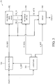
- the frequency generator 30 includes a frequency divider 300, a circulating delay circuit 302, a multiplexer (MUX) 304, a retimer 306 and a control unit 308.
- the control unit 308 is configured to receive an input signal CKIN, so as to generate a divisor signal S_DIV, a phase signal S_MUX and a circulation signal S_RET, which are used to control the elements of the frequency generator 30.
- the frequency divider 300 receives the input signal CKIN and is configured to perform an integer division to the input signal CKIN according to divisor signal S_DIV, so as to generate a frequency division signal CK_DIV.
- the circulating delay circuit 302 is coupled to the frequency divider 300 and configured to perform a circulating operation according to the frequency division signal CK_DIV, so as to generate at least one phase delay signals CK_1 ⁇ CK_M, wherein, the circulating delay circuit 302 may be calibrated in advance to adjust the delay of the phase delay signals CK_1 ⁇ CK_M, and may be used to repetitively perform the circulating operation, so that during each circulating operation, it may generate different phase delay signals CK_1 ⁇ CK_M.
- the multiplexer 304 is coupled to the circulating delay circuit 302 and configured to select one signal from frequency division signal CK_DIV and the phase delay signals CK_1 ⁇ CK_M according to the phase signal S_MUX, so as to generate a multiplexed signal CK_MUX.
- the retimer 306 is coupled to the frequency divider 300 and the multiplexer 304, and configured to generate an output signal CKOUT according to the frequency division signal CK_DIV and the circulation signal S_RET; in other words, by selecting the circulation signal S_RET, the retimer 306 may output the multiplexed signal CK_MUX as the output signal CKOUT at a correct circulating operation.
- the frequency generator 30 performs a fractional frequency division to the input signal CKIN to generate the output signal CKOUT.
- the frequency generator 30 uses a frequency divider 300 capable of changing the divisor to receive the input signal CKIN, so as to perform the integer division to the input signal CKIN, thereby generating the frequency division signal CK_DIV. It should be noted that since the frequency and period are reciprocal to each other, performing the division to the input signal CKIN using the frequency divider 300 means that the period of the input signal CKIN are increased by the integer multiple.
- the circulating delay circuit 302 receives the frequency division signal CK_DIV, and generate at least one phase delay signals CK_1 CK_M according to the frequency division signal CK_DIV, wherein, the circulating delay circuit 302 continuously performs the circulating operation and, for each circulating operation, generates the phase delay signals CK_1 ⁇ CK_M.
- the circulating delay circuit 302 may be adjusted using a calibration in advance, so that the phase or delay of the phase delay signal matches the requirement of the system; further, the phase differences between each phase delay signal CK_1 ⁇ CK_M are the same, and the frequency generator 30 may select an appropriate circulating operation and phase delay signal according to the system requirements, thereby obtaining an appropriate phase for performing the fractional frequency division operation.
- the multiplexer 304 receives the frequency division signal CK_DIV and M phase delay signals CK_1 ⁇ CK_M, and select one signal from the frequency division signal CK_DIV and M phase delay signals CK_1 ⁇ CK_M according to the phase signal S_MUX, wherein the selected signal is used as the multiplexed signal CK_MUX.
- the retimer 306 receives the multiplexed signal CK_MUX and is configured to output the multiplexed signal CK_MUX as the output signal CKOUT according to the circulation signal S_RET and the frequency division signal CK_DIV; in other words, the circulating delay circuit 302 continuously performs the circulating operation, and accordingly, for each circulating operation, the phase of the multiplexed signal CK_MUX selected by the multiplexer 304 would change, and the retimer 306 outputs the multiplexed signal CK_MUX as the output signal CKOUT during the correct circulating operation according to circulation signal S_RET, thereby accomplishing the fractional frequency division operation.
- the present disclosure uses the frequency divider 300 to perform the integer frequency division operation, so as to generate a frequency division signal CK_DIV having a period that is the integer multiple times of the input signal CKIN; uses the circulating delay circuit 302 to, at each circulating operation, generate at least one phase delay signals CK_1 ⁇ CK_M; uses the multiplexer 304 to select one signal from the frequency division signal CK_DIV and M phase delay signals CK_1 ⁇ CK_M as the multiplexed signal CK_MUX according to the phase signal; and uses the retimer 306 to obtain the phase of the phase delay signal during the correct circulating operation according to the circulation signal S_RET, so as to output the multiplexed signal CK_MUX as the output signal CKOUT.
- the present disclosure may use the limited circuit to generate phases continuously, and operate only when the CK_DIV is high, thereby reducing the power consumption; further, by using the multiplexer 304 and the retimer 306 to select the appropriate signal and delay, it achieves an open-loop and low-power frequency generator.
- the frequency generator 30 of the present disclosure may be configured to perform a fractional frequency division operation with a divisor of 17/5; in other words, the frequency generator 30 generates an output signal CKOUT with an output period Tout which is 17/5 times (i.e., 3+2/5 times) of the input period Tin of the input signal CKIN.
- the present disclosure by using the frequency divider 300 to perform the frequency division operation of the integer, to generate a frequency division signal CK_DIV having a period which is the integer multiple of the input period.
- the circulating delay circuit 302 is used to continuously perform the circulating operation, and for each circulating operation, generate a phase delay signal, and the multiplexer 304 and the retimer 306 are used to select the correct signal and circulating operation time, to compensate the insufficient frequency adjustment made by the frequency divider 300, thereby generating an output signal CKOUT having a period that is 3+2/5 times of the period of the input signal CKIN.
- the frequency divider 300 of the present disclosure can be designed as a frequency divider capable of performing an integer frequency division operation with a divisor of 3 or a divisor of 4, which may perform a frequency division operation to the input signal according to the divisor signal S_DIV.
- the circulating delay circuit 302 may be designed to generate two sets of phase delay signals CK_1, CK_2, and the delays of the phase delay signals CK_1, CK_2 are respectively 1/5 of the input period (i.e., Tin/5) and 2/5 of the input period (i.e., 2Tin/5); in this way, during the first circulating operation, the delays of the phase delay signals CK_1, CK_2 are respectively 1/5 of the input period Tin and 2/5 of the input period Tin; in the second circulating operation, the delays of the phase delay signals CK_1, CK_2 are respectively 3/5 of the input period Tin and 4/5 of the input period Tin; and so on; in this way, the circulating delay circuit 302 may generate different phase delay signals to make up for the frequency division operation with the insufficient frequency division signal CK_DIV.
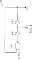
- FIG. 4 is a schematic diagram illustrating a circulating delay circuit 402 according to one embodiment of the present disclosure.
- the present circulating delay circuit 402 includes a NOT-AND gate NAND, and buffers BUF_1, BUF_2 that are serially connected to form a series, and buffers BUF_1, BUF_2 may respectively generate phase delay signals CK_1, CK_2.
- the circulating delay circuit 502 may perform gating using the NOT-AND gate NAND, wherein when the frequency division signal CK_DIV is high and delivered to the NOT-AND gate NAND, the serially connected series of buffers BUF_1, BUF_1 is switched on and continuously perform the circulating operations, and continuously generate the phase delay signals CK_1, CK_2; when the frequency division signal CK_DIV is low and delivered to the NOT-AND gate NAND, the serially connected series of buffers BUF_1, BUF_1 is switched off and do not perform the circulating operation, and hence do not output phase delay signals CK_1, CK_2. Further, the last buffer BUF_2 of the series feeds the phase delay signal CK_2 back to the NOT-AND gate NAND.
- the present frequency generator 30 may use the circulating delay circuit 302 to achieve the low-power frequency generator.
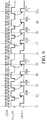
- FIG. 5 is a schematic diagram illustrating a retimer 506 according to one embodiment of the present disclosure.
- the retimer 506 includes N D-type flip-flops DFF1 ⁇ DFFn and a multiplexer MUX.
- the data output terminal of one D-type flip-flop is coupled to the data input terminal of another D-type flip-flop; accordingly, N D-type flip-flops are serially connected to form a series; in this case, the series of the D-type flip-flops DFF1 ⁇ DFFn is a shift register.
- the data input terminal of the D-type flip-flop DFF1 that is at the front end of the series is configured to receive the frequency division signal CK_DIV, and the frequency input terminals of all the D-type flip-flops DFF1 ⁇ DFFn in the series receive the multiplexed signal CK_MUX, so that a first retiming signal P_1 to an n th retiming signal P_n are respectively generated at the data output terminals of the D-type flip-flops DFF1 ⁇ DFFn, and the D-type flip-flops DFF1 ⁇ DFFn in the series may deliver the frequency division signal CK_DIV according to the trigger of the multiplexed signal CK_MUX, and wherein during the first circulating operation when the multiplexed signal CK_MUX triggers the D-type flip-flops DFF1 ⁇ DFFn for the first time, the D-type flip-flop DFF1 delivers the frequency division signal CK_DIV to the first retiming signal P_
- the retimer 506 may, upon the trigger of the multiplexed signal CK_MUX during different circulating operations, generate the retiming, and further by using the multiplexer MUX to select one signal from the first retiming signal P_1 to the n th retiming signal P_n as the output signal CKOUT according to the circulation signal S_RET, acquire the appropriate signal phase, thereby achieving an open-loop frequency generator for fractional-division operations.
- the frequency generator 30 may perform a fractional frequency division operation with a divisor of 17/5.
- the frequency divider 300 may perform a frequency division operation with a divisor of 3 or 4;
- the circulating delay circuit 302 may generate two sets of phase delay signals CK_1, CK_2, and the delays of the phase delay signals CK_1, CK_2 are respectively 1/5 of the input period Tin and 2/5 of the input period Tin;
- the multiplexer 304 selects one signal from the phase delay signals CK_1, CK_2 according to the phase signal, so as to generate a multiplexed signal CK_MUX;
- the retimer 306 generates an output signal CKOUT according to the trigger of a multiplexed signal CK_MUX and the instruction of a circulation signal S_RET.
- a divisor signal S_DIV generated by the control unit 308 instructs the frequency divider 300 to perform an integer frequency division operation to the input signal CKIN with a divisor of 3, so as to generate a frequency division signal CK_DIV; during each circulating operation, the circulating delay circuit 302 generates phase delay signals CK_1, CK_2 according to the frequency division signal CK_DIV; the phase signal S_MUX generated by the control unit 308 instructs the multiplexer 304 to select the phase delay signal CK_2 as the multiplexed signal CK_MUX; the circulation signal S_RET generated by the control unit 308 instructs the retimer 306 to select the multiplexed signal CK_MUX generated during the first circulating operation as the output signal CKOUT; in this way, by using the multiplexer 304 and the retimer 306 to select the phase delay signal CK_2 of the first circulating
- the frequency divider 300 uses the divisor of 3; the multiplexer 304 selects the phase delay signal CK_2 as the multiplexed signal CK_MUX; the retimer 306 selects the multiplexed signal CK_MUX generated during the third circulating operation as the output signal CKOUT according to the phase signal S_MUX; accordingly, the period of the frequency division signal CK_DIV may be increased by an additional 6/5 of the input period Tin.
- the divisor signal S_DIV instructs the frequency divider 300 to use a divisor of 4;
- the phase signal S_MUX instructs the multiplexer 304 to select the phase delay signal CK_1 as the multiplexed signal CK_MUX;
- the retimer 306 select the multiplexed signal CK_MUX generated during the second circulating operation as the output signal CKOUT according to the phase signal; accordingly the period of the frequency division signal CK_DIV may be increased by an additional 3/5 of the input period Tin.
- the frequency divider 300 uses the divisor of 4; the multiplexer 304 selects the frequency division signal CK_DIV as the multiplexed signal CK_MUX; the retimer 306 outputs the frequency division signal CK_DIV as the multiplexed signal CK_MUX.
- the frequency generator 30 may use the frequency divider 300 to perform the integer frequency division operation, use the circulating delay circuit 302 to continuously perform the circulating operation to generate phase delay signals CK_1, CK_2, use the multiplexer 304 and the retimer 306 to select the correct circulating operation and phase delay signal, and preferably adjust the period of the frequency division signal CK_DIV so as to generate the output signal CKOUT, thereby achieving an open-loop and low-power frequency generator.
- the time point T3 when the frequency divider 300 uses the divisor of 3, the period is increased by an addition which is 6/5 of the input period Tin by the circulating delay circuit 302, the multiplexer 304 and the retimer 306.
- the frequency divider 300 may perform a frequency division operation with a divisor of 4, the addition of the input period Tin is adjusted correspondingly to 1/5 of the input period Tin by the circulating delay circuit 302, multiplexer 304 and the retimer 306, so as to generate an appropriate output signal CKOUT.
- the divisors before and after the adjustment are the same (the divisor before the adjustment is (3+6/5), and the divisor after the adjustment is (4+1/5)).
- control unit 308 By using the control unit 308 to determine, in advance, the integer divisor and the amount of delay of the next frequency division signal CK_DIV whenever it receives a frequency division signal CK_DIV to generate a corresponding divisor signal S_DIV, phase signal S_MUX, and circulation signal S_RET to control the frequency divider 300, the circulating delay circuit 302, the multiplexer 304 and the retimer 306.
- the frequency division operation performed by the frequency generator 30 will result in the output period Tout being the (N+P/M) times of the output period Tin (i.e., the period and the frequency are reciprocal).
- the present disclosure may perform a frequency division operation to the input signal CKIN with a divisor of N or (N+1) by the frequency divider 300.
- the frequency division operation for the remaining divisor of P/M is implemented by the circulating delay circuit 302, the multiplexer 304 and the retimer 306.
- the divisor 17/5 equals (3+2/5)
- the frequency divider 300 may perform a frequency division operation with a divisor of 3 or a divisor of 4, whereas the frequency division operation for the remaining divisor of 2/5 are implemented by the circulating delay circuit 302, multiplexer 304 and the retimer 306.
- the delays of the phase delay signals CK_1 ⁇ CK_2 are respectively 1/5 of the input period Tin and 2/5 of the input period Tin, and each circulating operation delay is 2/5 of the input period Tin. It further selects an appropriate phase delay signal using the multiplexer 304 and selects a correct circulating operation using the retimer 306, and adjusts the duty cycle of the output signal CKOUT. In this way, the present frequency generator 30 may perform a frequency division operation of fractional-division to the input signal CKIN, so as to generate the output signal CKOUT.
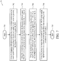
- the operation process described above with respect to a frequency generator performing a fractional frequency division operation to generate an output signal CKOUT according to an input signal CKIN may be summarized as a process 70, as shown in Figure 7 .
- the process 70 can be used in a frequency generator, wherein the frequency generator includes a frequency divider for receiving an input signal CKIN, and is configured to perform an integer frequency division operation to the input signal according to a divisor signal S_DIV, so as to generate a frequency division signal CK_DIV.
- a circulating delay circuit is coupled to the frequency divider and configured to continuously perform circulating operations according to the frequency division signal CK_DIV, wherein, during each circulating operation, the circulating delay circuit generates at least one phase delay signals CK_1 ⁇ CK_M.
- a multiplexer is coupled to the circulating delay circuit and configured to select one signal from the frequency division signal CK_DIV and the phase delay signals CK_1 ⁇ CK_M as a multiplexed signal CK_MUX according to a phase signal S_MUX.
- a retimer is coupled to the multiplexer and configured to generate an output signal CKOUT during the correct circulating operation time according to a circulation signal S_RET and the multiplexed signal CK_MUX.
- the process 70 includes the following steps:
Landscapes
- Engineering & Computer Science (AREA)
- Physics & Mathematics (AREA)
- General Engineering & Computer Science (AREA)
- Theoretical Computer Science (AREA)
- General Physics & Mathematics (AREA)
- Computer Hardware Design (AREA)
- Computing Systems (AREA)
- Mathematical Physics (AREA)
- Stabilization Of Oscillater, Synchronisation, Frequency Synthesizers (AREA)
- Manipulation Of Pulses (AREA)
- Pulse Circuits (AREA)
Applications Claiming Priority (1)
| Application Number | Priority Date | Filing Date | Title |
|---|---|---|---|
| PCT/CN2018/080993 WO2019183866A1 (fr) | 2018-03-29 | 2018-03-29 | Générateur de fréquence et procédé de génération de fréquence |
Publications (3)
| Publication Number | Publication Date |
|---|---|
| EP3573242A1 true EP3573242A1 (fr) | 2019-11-27 |
| EP3573242A4 EP3573242A4 (fr) | 2020-03-11 |
| EP3573242B1 EP3573242B1 (fr) | 2025-04-30 |
Family
ID=68062534
Family Applications (1)
| Application Number | Title | Priority Date | Filing Date |
|---|---|---|---|
| EP18897872.0A Active EP3573242B1 (fr) | 2018-03-29 | 2018-03-29 | Générateur de fréquence et procédé de génération de fréquence |
Country Status (4)
| Country | Link |
|---|---|
| US (1) | US10680620B2 (fr) |
| EP (1) | EP3573242B1 (fr) |
| CN (1) | CN110612667B (fr) |
| WO (1) | WO2019183866A1 (fr) |
Families Citing this family (7)
| Publication number | Priority date | Publication date | Assignee | Title |
|---|---|---|---|---|
| US10998911B1 (en) * | 2019-12-30 | 2021-05-04 | Nxp Usa, Inc. | Fractional N PLL with sigma-delta noise cancellation |
| US11356136B2 (en) * | 2020-09-08 | 2022-06-07 | Shenzhen GOODIX Technology Co., Ltd. | Harmonic rejection in multiphase signals |
| US11095293B1 (en) * | 2020-12-31 | 2021-08-17 | Texas Instruments Incorporated | Low-power fractional analog PLL without feedback divider |
| US11456760B1 (en) * | 2021-03-05 | 2022-09-27 | Motorola Solutions, Inc. | Linearizing narrowband carriers with low resolution predistorters |
| US11239846B1 (en) * | 2021-06-01 | 2022-02-01 | SambaNova Systems, Inc. | Variable-length clock stretcher with correction for glitches due to phase detector offset |
| WO2023081987A1 (fr) * | 2021-11-11 | 2023-05-19 | Robert Bosch Limitada | Procédé de contrôle d'un dispositif pour fonctionnement avec résolution fractionnaire |
| US12028079B2 (en) * | 2022-05-23 | 2024-07-02 | Texas Instruments Incorporated | Methods and apparatus to retime data using a programmable delay |
Family Cites Families (13)
| Publication number | Priority date | Publication date | Assignee | Title |
|---|---|---|---|---|
| US6671341B1 (en) * | 1999-09-17 | 2003-12-30 | Agere Systems, Inc. | Glitch-free phase switching synthesizer |
| US7012985B1 (en) * | 2004-07-30 | 2006-03-14 | Xilinx, Inc. | Frequency division of an oscillating signal involving a divisor fraction |
| US7756487B2 (en) * | 2006-08-29 | 2010-07-13 | Texas Instruments Incorporated | Local oscillator with non-harmonic ratio between oscillator and RF frequencies using pulse generation and selection |
| US7495517B1 (en) * | 2006-12-14 | 2009-02-24 | Altera Corporation | Techniques for dynamically adjusting the frequency range of phase-locked loops |
| CN101217277B (zh) * | 2008-01-15 | 2010-12-29 | 凌阳科技股份有限公司 | 非整数除频器以及可产生非整数时脉信号的锁相回路 |
| US7969209B2 (en) * | 2009-04-01 | 2011-06-28 | Skyworks Solutions, Inc. | Frequency divider circuit |
| CN102055466A (zh) * | 2009-11-06 | 2011-05-11 | 联咏科技股份有限公司 | 多相位信号产生装置 |
| US8461933B2 (en) * | 2010-10-26 | 2013-06-11 | Mediatek Inc. | Device and method for frequency calibration and phase-locked loop using the same |
| JP2012190510A (ja) * | 2011-03-11 | 2012-10-04 | Elpida Memory Inc | 半導体装置 |
| US8653862B2 (en) * | 2011-06-13 | 2014-02-18 | Mediatek Inc. | Frequency divider with retimed control signal and related frequency dividing method |
| US8873699B2 (en) * | 2012-11-21 | 2014-10-28 | Intel Mobile Communications GmbH | Fractional frequency divider with phase permutation |
| US20160380642A1 (en) * | 2014-03-12 | 2016-12-29 | Mediatek Singapore Pte. Ltd. | Divisor control circuit, fractional frequency division device, frequency synthesizer and frequency synthesis method |
| US9685966B2 (en) * | 2014-12-02 | 2017-06-20 | Mediatek Inc. | Fractional dividing module and related calibration method |
-
2018
- 2018-03-29 EP EP18897872.0A patent/EP3573242B1/fr active Active
- 2018-03-29 WO PCT/CN2018/080993 patent/WO2019183866A1/fr not_active Ceased
- 2018-03-29 CN CN201880000440.3A patent/CN110612667B/zh active Active
-
2019
- 2019-07-10 US US16/507,654 patent/US10680620B2/en active Active
Also Published As
| Publication number | Publication date |
|---|---|
| US20190334529A1 (en) | 2019-10-31 |
| EP3573242A4 (fr) | 2020-03-11 |
| EP3573242B1 (fr) | 2025-04-30 |
| CN110612667A (zh) | 2019-12-24 |
| US10680620B2 (en) | 2020-06-09 |
| WO2019183866A1 (fr) | 2019-10-03 |
| CN110612667B (zh) | 2023-05-02 |
Similar Documents
| Publication | Publication Date | Title |
|---|---|---|
| US10680620B2 (en) | Frequency generator and method for generating frequency | |
| US10972112B1 (en) | 50%-duty-cycle consecutive integer frequency divider and phase-locked loop circuit | |
| US8305119B2 (en) | Clock generation circuit | |
| US7777534B2 (en) | Fraction-N frequency divider and method thereof | |
| US6728526B2 (en) | Fractional-N frequency synthesizer with multiple clocks having different timings | |
| US20050200390A1 (en) | Highly configurable PLL architecture for programmable logic | |
| CN110350913A (zh) | 一种基于锁相延迟的多adc同步装置 | |
| CN104601171A (zh) | 小数分频器和小数分频锁相环 | |
| US6779010B2 (en) | Accumulator with programmable full-scale range | |
| CN101256229A (zh) | 接收设备 | |
| CN114389599A (zh) | 小数-n锁相环及其电荷泵控制方法 | |
| US8035451B2 (en) | On-the-fly frequency switching while maintaining phase and frequency lock | |
| EP2963826A1 (fr) | Circuit synthétiseur de fréquence | |
| JPH1155108A (ja) | プレスケーラとその後に続くプログラマブルカウンタを有する周波数分割器、および対応するプレスケーラならびに周波数合成器 | |
| KR20180006964A (ko) | 주파수 분할기, 위상-동기 루프, 트랜시버, 무선국 및 주파수 분할 방법 | |
| CN113783569A (zh) | 一种低功耗的频率综合器 | |
| TWI569582B (zh) | 時脈資料回復裝置、時脈資料回復方法及相位偵測器 | |
| CN102291119B (zh) | 分频装置及方法 | |
| US8768994B2 (en) | Filter auto-calibration using multi-clock generator | |
| EP1889366B1 (fr) | Generateur d'echelles destine a un synthetiseur n-fractionnel | |
| CN110504961B (zh) | 一种多模预分频器及其分频方法 | |
| JP2017512446A (ja) | 周波数シンセサイザ | |
| US11437985B1 (en) | Duty cycle correction circuit | |
| US6359948B1 (en) | Phase-locked loop circuit with reduced jitter | |
| US7167685B2 (en) | Frequency division |
Legal Events
| Date | Code | Title | Description |
|---|---|---|---|
| STAA | Information on the status of an ep patent application or granted ep patent |
Free format text: STATUS: UNKNOWN |
|
| STAA | Information on the status of an ep patent application or granted ep patent |
Free format text: STATUS: THE INTERNATIONAL PUBLICATION HAS BEEN MADE |
|
| PUAI | Public reference made under article 153(3) epc to a published international application that has entered the european phase |
Free format text: ORIGINAL CODE: 0009012 |
|
| STAA | Information on the status of an ep patent application or granted ep patent |
Free format text: STATUS: REQUEST FOR EXAMINATION WAS MADE |
|
| 17P | Request for examination filed |
Effective date: 20190710 |
|
| AK | Designated contracting states |
Kind code of ref document: A1 Designated state(s): AL AT BE BG CH CY CZ DE DK EE ES FI FR GB GR HR HU IE IS IT LI LT LU LV MC MK MT NL NO PL PT RO RS SE SI SK SM TR |
|
| AX | Request for extension of the european patent |
Extension state: BA ME |
|
| A4 | Supplementary search report drawn up and despatched |
Effective date: 20200210 |
|
| RIC1 | Information provided on ipc code assigned before grant |
Ipc: H03K 23/68 20060101ALI20200204BHEP Ipc: H03L 7/24 20060101AFI20200204BHEP Ipc: G06F 1/02 20060101ALI20200204BHEP Ipc: H03L 7/197 20060101ALI20200204BHEP |
|
| DAV | Request for validation of the european patent (deleted) | ||
| DAX | Request for extension of the european patent (deleted) | ||
| STAA | Information on the status of an ep patent application or granted ep patent |
Free format text: STATUS: EXAMINATION IS IN PROGRESS |
|
| 17Q | First examination report despatched |
Effective date: 20211019 |
|
| GRAP | Despatch of communication of intention to grant a patent |
Free format text: ORIGINAL CODE: EPIDOSNIGR1 |
|
| STAA | Information on the status of an ep patent application or granted ep patent |
Free format text: STATUS: GRANT OF PATENT IS INTENDED |
|
| INTG | Intention to grant announced |
Effective date: 20250117 |
|
| GRAS | Grant fee paid |
Free format text: ORIGINAL CODE: EPIDOSNIGR3 |
|
| GRAA | (expected) grant |
Free format text: ORIGINAL CODE: 0009210 |
|
| STAA | Information on the status of an ep patent application or granted ep patent |
Free format text: STATUS: THE PATENT HAS BEEN GRANTED |
|
| AK | Designated contracting states |
Kind code of ref document: B1 Designated state(s): AL AT BE BG CH CY CZ DE DK EE ES FI FR GB GR HR HU IE IS IT LI LT LU LV MC MK MT NL NO PL PT RO RS SE SI SK SM TR |
|
| REG | Reference to a national code |
Ref country code: CH Ref legal event code: EP Ref country code: GB Ref legal event code: FG4D |
|
| REG | Reference to a national code |
Ref country code: DE Ref legal event code: R096 Ref document number: 602018081623 Country of ref document: DE |
|
| REG | Reference to a national code |
Ref country code: IE Ref legal event code: FG4D |
|
| REG | Reference to a national code |
Ref country code: NL Ref legal event code: MP Effective date: 20250430 |
|
| REG | Reference to a national code |
Ref country code: AT Ref legal event code: MK05 Ref document number: 1791055 Country of ref document: AT Kind code of ref document: T Effective date: 20250430 |
|
| PG25 | Lapsed in a contracting state [announced via postgrant information from national office to epo] |
Ref country code: PT Free format text: LAPSE BECAUSE OF FAILURE TO SUBMIT A TRANSLATION OF THE DESCRIPTION OR TO PAY THE FEE WITHIN THE PRESCRIBED TIME-LIMIT Effective date: 20250901 Ref country code: FI Free format text: LAPSE BECAUSE OF FAILURE TO SUBMIT A TRANSLATION OF THE DESCRIPTION OR TO PAY THE FEE WITHIN THE PRESCRIBED TIME-LIMIT Effective date: 20250430 Ref country code: ES Free format text: LAPSE BECAUSE OF FAILURE TO SUBMIT A TRANSLATION OF THE DESCRIPTION OR TO PAY THE FEE WITHIN THE PRESCRIBED TIME-LIMIT Effective date: 20250430 |
|
| REG | Reference to a national code |
Ref country code: LT Ref legal event code: MG9D |
|
| PG25 | Lapsed in a contracting state [announced via postgrant information from national office to epo] |
Ref country code: NO Free format text: LAPSE BECAUSE OF FAILURE TO SUBMIT A TRANSLATION OF THE DESCRIPTION OR TO PAY THE FEE WITHIN THE PRESCRIBED TIME-LIMIT Effective date: 20250730 Ref country code: GR Free format text: LAPSE BECAUSE OF FAILURE TO SUBMIT A TRANSLATION OF THE DESCRIPTION OR TO PAY THE FEE WITHIN THE PRESCRIBED TIME-LIMIT Effective date: 20250731 |
|
| PG25 | Lapsed in a contracting state [announced via postgrant information from national office to epo] |
Ref country code: PL Free format text: LAPSE BECAUSE OF FAILURE TO SUBMIT A TRANSLATION OF THE DESCRIPTION OR TO PAY THE FEE WITHIN THE PRESCRIBED TIME-LIMIT Effective date: 20250430 Ref country code: NL Free format text: LAPSE BECAUSE OF FAILURE TO SUBMIT A TRANSLATION OF THE DESCRIPTION OR TO PAY THE FEE WITHIN THE PRESCRIBED TIME-LIMIT Effective date: 20250430 |
|
| PG25 | Lapsed in a contracting state [announced via postgrant information from national office to epo] |
Ref country code: BG Free format text: LAPSE BECAUSE OF FAILURE TO SUBMIT A TRANSLATION OF THE DESCRIPTION OR TO PAY THE FEE WITHIN THE PRESCRIBED TIME-LIMIT Effective date: 20250430 |
|
| PG25 | Lapsed in a contracting state [announced via postgrant information from national office to epo] |
Ref country code: HR Free format text: LAPSE BECAUSE OF FAILURE TO SUBMIT A TRANSLATION OF THE DESCRIPTION OR TO PAY THE FEE WITHIN THE PRESCRIBED TIME-LIMIT Effective date: 20250430 |
|
| PG25 | Lapsed in a contracting state [announced via postgrant information from national office to epo] |
Ref country code: AT Free format text: LAPSE BECAUSE OF FAILURE TO SUBMIT A TRANSLATION OF THE DESCRIPTION OR TO PAY THE FEE WITHIN THE PRESCRIBED TIME-LIMIT Effective date: 20250430 |
|
| PG25 | Lapsed in a contracting state [announced via postgrant information from national office to epo] |
Ref country code: RS Free format text: LAPSE BECAUSE OF FAILURE TO SUBMIT A TRANSLATION OF THE DESCRIPTION OR TO PAY THE FEE WITHIN THE PRESCRIBED TIME-LIMIT Effective date: 20250731 |
|
| PG25 | Lapsed in a contracting state [announced via postgrant information from national office to epo] |
Ref country code: IS Free format text: LAPSE BECAUSE OF FAILURE TO SUBMIT A TRANSLATION OF THE DESCRIPTION OR TO PAY THE FEE WITHIN THE PRESCRIBED TIME-LIMIT Effective date: 20250830 |
|
| PG25 | Lapsed in a contracting state [announced via postgrant information from national office to epo] |
Ref country code: LV Free format text: LAPSE BECAUSE OF FAILURE TO SUBMIT A TRANSLATION OF THE DESCRIPTION OR TO PAY THE FEE WITHIN THE PRESCRIBED TIME-LIMIT Effective date: 20250430 |
|
| PG25 | Lapsed in a contracting state [announced via postgrant information from national office to epo] |
Ref country code: DK Free format text: LAPSE BECAUSE OF FAILURE TO SUBMIT A TRANSLATION OF THE DESCRIPTION OR TO PAY THE FEE WITHIN THE PRESCRIBED TIME-LIMIT Effective date: 20250430 Ref country code: SM Free format text: LAPSE BECAUSE OF FAILURE TO SUBMIT A TRANSLATION OF THE DESCRIPTION OR TO PAY THE FEE WITHIN THE PRESCRIBED TIME-LIMIT Effective date: 20250430 |
|
| PG25 | Lapsed in a contracting state [announced via postgrant information from national office to epo] |
Ref country code: CZ Free format text: LAPSE BECAUSE OF FAILURE TO SUBMIT A TRANSLATION OF THE DESCRIPTION OR TO PAY THE FEE WITHIN THE PRESCRIBED TIME-LIMIT Effective date: 20250430 |
|
| PG25 | Lapsed in a contracting state [announced via postgrant information from national office to epo] |
Ref country code: EE Free format text: LAPSE BECAUSE OF FAILURE TO SUBMIT A TRANSLATION OF THE DESCRIPTION OR TO PAY THE FEE WITHIN THE PRESCRIBED TIME-LIMIT Effective date: 20250430 |
|
| PG25 | Lapsed in a contracting state [announced via postgrant information from national office to epo] |
Ref country code: SK Free format text: LAPSE BECAUSE OF FAILURE TO SUBMIT A TRANSLATION OF THE DESCRIPTION OR TO PAY THE FEE WITHIN THE PRESCRIBED TIME-LIMIT Effective date: 20250430 Ref country code: RO Free format text: LAPSE BECAUSE OF FAILURE TO SUBMIT A TRANSLATION OF THE DESCRIPTION OR TO PAY THE FEE WITHIN THE PRESCRIBED TIME-LIMIT Effective date: 20250430 |
|
| PG25 | Lapsed in a contracting state [announced via postgrant information from national office to epo] |
Ref country code: IT Free format text: LAPSE BECAUSE OF FAILURE TO SUBMIT A TRANSLATION OF THE DESCRIPTION OR TO PAY THE FEE WITHIN THE PRESCRIBED TIME-LIMIT Effective date: 20250430 |
|
| REG | Reference to a national code |
Ref country code: DE Ref legal event code: R097 Ref document number: 602018081623 Country of ref document: DE |
|
| PLBE | No opposition filed within time limit |
Free format text: ORIGINAL CODE: 0009261 |
|
| STAA | Information on the status of an ep patent application or granted ep patent |
Free format text: STATUS: NO OPPOSITION FILED WITHIN TIME LIMIT |
|
| REG | Reference to a national code |
Ref country code: CH Ref legal event code: L10 Free format text: ST27 STATUS EVENT CODE: U-0-0-L10-L00 (AS PROVIDED BY THE NATIONAL OFFICE) Effective date: 20260311 |
|
| 26N | No opposition filed |
Effective date: 20260202 |
|
| PGFP | Annual fee paid to national office [announced via postgrant information from national office to epo] |
Ref country code: DE Payment date: 20260324 Year of fee payment: 9 |