EP3574351B1 - Dispositif plasmonique - Google Patents
Dispositif plasmonique Download PDFInfo
- Publication number
- EP3574351B1 EP3574351B1 EP18744858.4A EP18744858A EP3574351B1 EP 3574351 B1 EP3574351 B1 EP 3574351B1 EP 18744858 A EP18744858 A EP 18744858A EP 3574351 B1 EP3574351 B1 EP 3574351B1
- Authority
- EP
- European Patent Office
- Prior art keywords
- metal
- plasmonic
- stripes
- layer
- grating
- Prior art date
- Legal status (The legal status is an assumption and is not a legal conclusion. Google has not performed a legal analysis and makes no representation as to the accuracy of the status listed.)
- Active
Links
Images


Classifications
-
- G—PHYSICS
- G02—OPTICS
- G02B—OPTICAL ELEMENTS, SYSTEMS OR APPARATUS
- G02B5/00—Optical elements other than lenses
- G02B5/008—Surface plasmon devices
-
- G—PHYSICS
- G02—OPTICS
- G02B—OPTICAL ELEMENTS, SYSTEMS OR APPARATUS
- G02B5/00—Optical elements other than lenses
- G02B5/18—Diffraction gratings
- G02B5/1809—Diffraction gratings with pitch less than or comparable to the wavelength
-
- G—PHYSICS
- G01—MEASURING; TESTING
- G01N—INVESTIGATING OR ANALYSING MATERIALS BY DETERMINING THEIR CHEMICAL OR PHYSICAL PROPERTIES
- G01N21/00—Investigating or analysing materials by the use of optical means, i.e. using sub-millimetre waves, infrared, visible or ultraviolet light
- G01N21/17—Systems in which incident light is modified in accordance with the properties of the material investigated
- G01N21/55—Specular reflectivity
- G01N21/552—Attenuated total reflection
- G01N21/553—Attenuated total reflection and using surface plasmons
- G01N21/554—Attenuated total reflection and using surface plasmons detecting the surface plasmon resonance of nanostructured metals, e.g. localised surface plasmon resonance
Definitions
- the invention relates to surface plasmonic (SP) devices to enhance optical processes in samples in the proximity of the device.
- SP surface plasmonic
- the invention relates to design and fabrication of plasmonic devices for linear and nonlinear microscopy and spectroscopy applications in physics, chemistry, biology, bioimaging and medical diagnostics field, for example.
- SP surface plasmonic
- SP nanostructures allow to manipulate light at nanoscale, which has potential to transform chemical, biological and medical imaging and sensing applications.
- SHG second harmonic generation
- TMG third harmonic generation
- FSG sum frequency generation
- TPEF two photon excited fluorescence
- Biomedical optical imaging techniques are playing a substantial role in the diagnosis, prevention and treatment of various diseases.
- Optical microscopy is widely used to visualize molecules in medicine and in biosciences.
- optical microscopes including the super-resolution microscopes, high-intensity light is directed onto a sample, which is placed on a coverslip glass.
- biological materials i.e., typically cells or tissues
- essentially all molecules and a large fraction of subcellular organelles are smaller than the lateral and depth resolution of conventional confocal microscopes. This is an obstacle for visualizing these structures in detail.
- sensitivity of detection is a major bottleneck: the number of molecules may be too small to be detected or only a small fraction of them can be detected.
- Fluorescence microscopy is one the most widely used imaging methods in biology by means of its molecular and chemical specificity.
- the fluorescence microscope is based on the phenomenon that certain materials, for example fluorophores or dyes have large absorption cross-sections at a specific wavelength and emit light at a longer wavelength when irradiated with the light of a specific wavelength.
- the fluorescent species-labeled molecules are very bright and distinguishable in fluorescence microscopy imaging.
- Raman spectroscopy is widely used method to identity the molecules by means of their vibrational, rotational, and low-frequency modes.
- conventional Raman spectroscopy high-intensity monochromatic light, usually from a laser in the visible or near infrared is directed onto a sample. The photons are absorbed or emitted by the sample and also the scattered photons are shifted up or down. The shift in energy provides the information about the phonon modes in the system.
- Spontaneous or conventional Raman scattering is very week with a cross-section of ⁇ 10-30cm 2 and 1 in 107 photons are inelastically scattered by the sample molecules.
- CARS coherent anti-Stokes Raman scattering
- SRS stimulated Raman scattering
- TERS tip-enhanced Raman scattering
- HR Hyper Raman
- Resonance Raman spatially offset Raman spectroscopy
- Angle-resolved Raman spectroscopy have been applied to increase the sensitivity.
- CARS, Hyper Raman (HR) and SRS utilize the nonlinear processes.
- the CARS signal will be enhanced, if the pump or Stokes excitation wavelengths are in resonance with the surface plasmons of plasmonic nanostructures on which the molecules are positioned.
- SECARS has been proposed to increase the signal sensitivity significantly using nanostructured metal surfaces.
- the detection, identification and molecular imaging of different chemical and biological composition species inside a sample with nano-sized particles sensitivity using CARS spectroscopy has not been done.
- the detection and visualization of plasma membrane has remained a challenge.
- the embodiments of this invention address these problems in the current state of the art and potential applications in biology, bioimaging, medical diagnostic, pathology, toxicology, forensics, cosmetics, chemical analysis and numerous other fields.
- Figures 1A and 1B One prior art nanostructure device is depicted in Figures 1A and 1B , where Figure 1A illustrates a prior art plasmonic nanohole array and Figure 1B illustrates a top-view SEM image of the prior art nanohole array.
- Figure 2A illustrates an exemplary emission spectrum of a gold nanohole array using the excitation wavelength of 780 nm according to the prior art nanohole array
- Figure 2B illustrates an exemplary emission spectrum of a gold nanohole array using the combination of excitation wavelengths of 817 nm and 1064 nm according to the prior art nanohole array.
- the background disturbing luminescence in Figure 2A comes from the two-photon excitation process, and the disturbing SFG, SGH, and FWM peaks can be seen on top of the broad TPEL emission spectrum in Figure 2B .
- FIG. 2A shows the TPEL of the nanohole array in thin gold film with a periodicity of 400 nm with excitation wavelength of 780 nm.
- the TPEL shows a broad peak in the range of 550-675 nm that is centered at about 625 nm.
- the nanohole array with 400 nm periodicity shows transmission maxima of the localized surface plasmon peaks (1,1) and (1,0) at 610 nm and 780 nm, respectively.
- the localized surface plasmon wavelength (1,0) of the nanohole array resonates with the excitation wavelength of 780 nm, which enhances the nonlinear TPEL intensity.
- the nanoholes array can be used in TPEF spectroscopy for high sensivity molecular imaging.
- Figure 2B shows the nonlinear coherent emission spectrum of a nanohole array with a periodicity of 400 using the combination of pump wavelength of 817 nm and the Stokes wavelength of 1064 nm laser.
- the spectra show the SFG, SHG and FWM signals on top of the broad band TPEL.
- the SFG and SHG peaks are related to the plasmon-enhanced second order coherent response and the FWM signal corresponds to the plasmon-enhanced third order coherent response.
- the second and third order nonlinear responses are influenced by the geometrical symmetry of the nanohole arrays.
- Plasmonic devices for enhancing optical processes in samples are known e.g. from US2011/267613 , US2008/316490 , and US2011/085172 .
- An object of the invention is to alleviate and eliminate the problems relating to the known prior art.
- the object of the invention is to provide a surface plasmonic device that enhances electric field at the surface or in the proximity of the plasmonic device, and most advantageously produces an enhanced electric near field in the vicinity of the metal so that to provide as uniform near field distribution as possible, and not rely on hot-spots, like many SERS techniques do.
- This enhancement is advantageous in various microscopic and spectroscopic measurements.
- it is advantageous when using light on certain frequencies, such as narrow frequency band LED light and laser light that utilize laser light to excite optical processes in samples lying on or in the proximity of the surface of the device.
- object of the invention is to avoid disturbing background signals and at the same time also enable large laser powers to be used without a significant risk to damaging the plasmonic device, such as evaporating the structure material of the nanostructured device.
- the object advantageously may also allow use of lower light intensities to reach clear images while limiting the heating of the plasmonic device and the sample being investigated that can be advantageous especially in some areas of biological microscopy.
- object of the invention is to provide and develop the plasmonic device, which is suitable for microscopy linear and nonlinear spectroscopy, and particularly for laser-based microscopy and spectroscopy.
- the present invention relates to the design and fabrication of surface plasmonic (SP) nanostructures, such as nanogratings, for linear and nonlinear spectroscopy, microscopy and imaging applications in physics, chemistry, biology, and medical sciences.
- SP surface plasmonic
- SPPs Surface plasmon polaritons
- SPPs are collective oscillations of free electrons at the interface between a metal and a dielectric. This produces an enhanced electric near field in the vicinity of the metal.
- nanogratings can be used.
- the design principle here is to provide as uniform near field distribution as possible, and not to rely on hot-spots, like many SERS techniques do.
- the invention relates to a plasmonic device to enhance optical processes in samples on or in the proximity of the device according to claim 1.
- the invention relates to a manufacturing method for manufacturing the plasmonic device according to claim 13.
- the plasmonic device is configured to enhance optical processes in samples lying on or in the proximity of the surface of the plasmonic device.
- the plasmonic devices are generally configured to enhance the optical processes of Raman scattering (RS), linear and nonlinear surface enhanced Raman scattering (SERS), coherent anti-Stokes Raman scattering (CARS) and surface enhanced coherent anti-Stokes Raman scattering (SECARS), but in addition to also to enhance the optical processes of fluorescence, second harmonic generation (SHG), sum frequency generation (SFG), and two photon excited fluorescence (TPEF) and all non-linear processes.
- RS Raman scattering
- SERS linear and nonlinear surface enhanced Raman scattering
- CARS coherent anti-Stokes Raman scattering
- SECARS surface enhanced coherent anti-Stokes Raman scattering
- the plasmonic structures according to advantageous embodiment of the invention comprise nanograting structures with elongated grooves and comprise also advantageously predefined continuous shape and patterns for enhancing four wave mixing (FWM) signal intensity without two photon excited luminescence (TPEL) background in SECARS imaging.
- FWM four wave mixing
- TPEL photon excited luminescence
- the plasmonic device comprises a substrate and the plasmonic structure.
- the plasmonic structure according to the embodiment comprises both a (full) metal layer and a metal grating in connection with the metal layer, advantageously next to the metal layer.
- the plasmonic device may also comprise an adhesion layer between the substrate and the plasmonic structure.
- the plasmonic device may also comprise a protective layer above the metal layer or metal grating. It is to be noted that the adhesion layer and the protective layer are optional, but useful in some embodiments as described elsewhere in this document.
- the metal grating of the device comprises elongated metal stripes and elongated empty spacing or grooves between the stripes.
- the thickness of the metal grating is advantageously in the range of 5 - 500 nm, and the width of the elongated metal stripes in the metal grating is advantageously in the range of 10 - 1000 nm.
- the empty spacing or grooves between the two adjacent elongated metal stripes in the metal grating is advantageously in the range of 10 - 1000 nm.
- the periodicity is described as of the adjacent elongated metal stripes in the metal grating comprising the sum of the width of one elongated metal stripe and the width of the empty spacing or grooves of two adjacent elongated metal stripes.
- the periodicity is advantageously selected to resonate with either the molecular vibrational frequency of a substance in the sample or the frequency of the exciting laser light or both of them.
- the periodicity in the metal grating is in the range of 10 - 1000 nm.
- the device may comprise the optional protective layer on top the structure.
- the thickness of the protective layer is in the range of 1 - 50 nm, and the protective layer comprises any dielectric materials, such as Al 2 O 3 , TiO 2 , SiO 2 .
- the device may comprise also the optional adhesion layer, which is advantageously deposited using materials, such as chromium, titanium and TiO 2 .
- the thickness of the adhesion layer (002) is advantageously in the range of about 1 - 50 nm.
- the substrate of the plasmonic device can advantageously comprise any material, the most usual being coverslip glass (borosilicate glass), normal glass (silica glass), quartz, calcium fluoride (CaF 2 ) and silicon.
- the thickness of the substrate is advantageously in the range of 50 ⁇ m - 5 mm.
- the (full) metal layer and/or the metal grating comprise any plasmonic materials, such as gold, silver, copper, platinum, palladium, aluminium, or any other material that enhances the optical processes.
- the thickness of the full metal layer is in the range of 50 - 100 nm.
- the plasmonic structure described here comprises advantageously nanostructures, such as layers and/or predefined continuous shapes and patterns, such as grooves, for enhancing four wave mixing (FWM) signal intensity without two photon excited luminescence (TPEL) background in SECARS imaging.
- the spacing between the two adjacent elongated grooves is advantageously in the range of about 10-1000 nm.
- the continuous shape and patterns can be described by a periodicity (periodicity of the two adjacent elongated grooves), which comprises the width of the two adjacent elongated grooves and the spacing of the two adjacent elongated grooves.
- the plasmonic device described in this document is therefore configured to enhance the optical processes of Raman scattering (RS), linear and nonlinear surface enhanced Raman scattering (SERS), coherent anti-Stokes Raman scattering (CARS) and surface enhanced coherent anti-Stokes Raman scattering (SECARS), stimulated Raman scattering (SRS), Hyper Raman (HR).
- RS Raman scattering
- SERS linear and nonlinear surface enhanced Raman scattering
- CARS coherent anti-Stokes Raman scattering
- SECARS surface enhanced coherent anti-Stokes Raman scattering
- SRS stimulated Raman scattering
- HR Hyper Raman
- the plasmonic device is configured to enhance the optical processes of fluorescence, multiphoton fluorescence, total internal reflection, second harmonic generation (SHG), third harmonic generation (THG), sum frequency generation (SFG), and two photon excited fluorescence (TPEF).
- the structure and dimensions and thicknesses of the nanostructures of the plasmonic device according to embodiments of the present invention offers clear advantages over the known prior art, namely for example the disturbing background signals especially in FWM or CARS imaging of nano-sized features can be avoided.
- due to spacing between the two adjacent elongated grooves or other features as well as other dimensions of the material of the plasmonic device does not evaporate even with relative strong pulsed laser powers, which is the problem especially with the nanohole structures or nanoantennas in the prior art.
- the plasmonic device according to the present invention can be manufactured for example by providing a plasmonic structure 008 comprising a (full) metal layer 003 and a metal grating 004 on a substrate layer 001 using electron beam lithography (EBL) or nanoimprint lithography (NIL) techniques and lift-off or wet or dry etching process.
- EBL electron beam lithography
- NIL nanoimprint lithography
- the providing of the plasmonic structure comprising a full metal layer 003 and/or a metal grating 004 is advantageously performed by using electron beam lithography (EBL) or nanoimprint lithography (NIL) techniques, and the lift-off technique or by wet or dry etching process.
- EBL electron beam lithography
- NIL nanoimprint lithography
- Providing of the optional protective layer is advantageously performed by using deposition methods such as vacuum evaporation, sputtering, plasma enhanced chemical vapor deposition (PECVD), and atomic layer deposition (ALD).
- the present invention offers advantages over the known prior art.
- the plasmonic nanostructured devices according to the invention have a predefined shape or dimensions, arrangement and pattern which results in the strong enhancement of a number of optical phenomena, such as reflectance, absorption, extraordinary optical transmission, linear and nonlinear Raman scattering processes, FWM, SHG, THG, SFG, TPEL and other optical effects.
- the present invention relates to the SP nanostructures optical resonance phenomena with the excited laser light wavelength and molecular vibrational frequency for strong enhancement of linear and nonlinear Raman scattering processes and fluorescent dye or fluorophores.
- the device may be implemented e.g. on a coverslip glass that can be inserted in a microscope in place of a current coverslip glass, suitable for use for example in laser microscopy.
- the device is preferably designed so that light is shown and collected from the top side of the device, where also the sample to be imaged is located (not for example light coming from below).
- the present invention is directed to surface plasmonic (SP) structures having well defined features at predetermined locations on a substrate for enhancing optical signal resulting from enhanced optical processes used in linear and nonlinear spectroscopy, microscopy and imaging techniques, such as SERS, SECARS and SRS.
- SP surface plasmonic
- the plasmonic device can be constructed in several ways, but it advantageously comprises at least one metal layer 003 and a 1-dimensional metal grating 004 consisting of metal stripes.
- the adhesive layer 002 is usually advantageous with metallic layers, but it is not necessary in some cases, thus being optional.
- the next layer is the thin metal layer 003.
- On top of the metal layer there is the 1-dimensional metal grating 004 comprising elongated metal stripes 005 and elongated empty spacing or grooves 006 between the stripes is fabricated.
- a protective layer can be added on top of the nanostructure 008, especially when using materials which oxidise easily.
- the operation of the device is based on advantageous formation of surface plasmon-polaritons in the interface between the metal grating and the measurement medium.
- the thicknesses of the layers and the dimensions of the grating are designed to enhance the electric field on the surface of the device when light with a known wavelength or wavelengths, typically from lasers or light emitting diodes (LEDs), is directed to the device.
- the thickness of the underlying substrate 001 is in the range of 50 ⁇ m - 5 mm, and the thickness of the optional adhesion layer 002 is in the range of about 1 - 50 nm.
- the thickness of the (full) metal layer 003 is in the range of 50 nm - 100 nm, and the thickness of the metal grating 004 is advantageously in the range of 5 - 100 nm.
- the width 005 of the elongated metal stripes in the metal grating 004 is advantageously in the range of 10 - 1000 nm, and the empty spacing or grooves 006 between the two adjacent elongated metal stripes in the metal grating 004 is in the range of 10 - 1000 nm.
- the stripes in the metal grating 004 are advantageously continuous with a length of at least 10 ⁇ m, reaching even 5 cm in large-area substrates. This is different for example from the nanoantennas used in certain techniques, thereby offering as uniform near field distribution as possible, and not relying on hot-spots as is the case e.g. with the nanohole and nanoantenna structures.
- a periodicity 007 of the adjacent elongated metal stripes in the metal grating 004 comprises the sum of the width 005 of one elongated metal stripe and the width 006 of the empty spacing or grooves of two adjacent elongated metal stripes.
- the periodicity 007 is advantageously selected to resonate with either the molecular vibrational frequency of a substance in the sample or the frequency of the exciting laser (or LED) light or both of them.
- the periodicity 007 in the metal grating 004 is advantageously in the range of 10 - 1000 nm.
- the device 100 comprises a protective layer covering advantageously the whole surface.
- the thickness of the protective layer is advantageously in the range of 1 - 50 nm.
- the substrate 001 of the plasmonic device 100 comprises materials, such as coverslip glass (borosilicate), normal glass (silica), quartz, calcium fluoride (CaF 2 ), and silicon.
- the adhesion layer 002 is deposited using materials, such as chromium, titanium or and TiO 2 .
- the (full) metal layer 003 and the metal grating 004 comprises any plasmonic materials, such as gold, silver, copper, platinum, palladium, aluminium, or any other material which is able to maintain surface plasmon-polaritons.
- the protective layer comprises advantageously any dielectric materials, such as Al 2 O 3 , TiO 2 , SiO 2 .
- the periodicity 007 includes the 005 and 006 and is selected to resonate with the molecular vibrational frequency and excited laser light frequency.
- Figure 3B shows a scanning electron microscopy (SEM) image of an exemplary embodiment 100 of the presented invention from a top-view, where the width 005 of one elongated metal stripe and the width 006 of the empty spacing or grooves of two adjacent elongated metal stripes and thereby the periodicity 007 can be clearly seen.
- SEM scanning electron microscopy
- This SP structure was fabricated on a coverslip glass substrate using electron beam lithography (EBL) to form the pattern.
- EBL electron beam lithography
- a 5 nm thick titanium adhesion layer followed by 60 nm thick gold layer were deposited by a metal evaporator in this exemplary embodiment.
- After spinning of the resist and the EBL exposure of the pattern another gold layer was deposited and a lift-off process was used to form the well-defined grating structure as shown in the SEM image of Figure 3B .
- This configuration has been shown to resonate with the exciting laser light frequency to enhance the linear and nonlinear Raman scattered intensity by two orders of magnitude in CARS imaging.
- the thickness of the underlying continuous metal layer 003 is crucial for heat conduction in pulsed light CARS imaging. In the measurements of the exemplary embodiment and with strong laser powers thickness over 50 nm has been found beneficial for the underlying continuous metal layer 003.
- GFP green fluorescent protein
- the present invention relates to SP nanostructures having predefined shape, arrangement and pattern which results in the strong enhancement of a number of optical phenomena, such as reflectance, absorption, extraordinary optical transmission, linear and nonlinear Raman scattering processes, FWW, SHG, SFG, TPEL and other optical effects.
- the SP nanostructures are designed to resonate with the excited laser (or LED) light wavelength and molecular vibrational frequency of the substance to be detected.
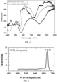
- Figure 4 illustrates an exemplary embodiment of an optical reflectance measurement of a 1-dimensional grating structure made of gold in contact with materials having various refractive indexes according to an advantageous embodiment of the invention.
- This preferred embodiment has a SP nanograting structure with a grating layer 004 thickness of 60 nm, stripe width 005 of 220 nm, spacing 006 of 100 nm and periodicity 007 of 320 nm on an area of 30 ⁇ 30 ⁇ m 2 , for example.
- This structure resonates at the wavelength of 817 nm when the medium is air.
- the optical reflectance properties of the SP nanograting structures were characterized with varying refractive indexes of 1 (air), 1.33 (water) and 1.49 (PMMA).
- the incident TM polarized light was illuminated along the SP nanograting structure and the reflected light was collected by the optical spectrometer.
- the measurement spectra show the surface plasmon resonance wavelengths with respect to the predefined SP nanograting structures.
- This present invention relates to the use of SP nanograting structures as disclosed herein to resonate with the excited laser beam and molecular vibrational frequency for enhancing linear and nonlinear Raman scattering, TPEL, SHG, SFG and FWM signal intensity.
- the periodicity 007 of the grating can be selected using the formula presented elsewhere in this document. Then, the thickness 004 of the grating as well as the width of the elongated metal stripes 005 and width of the grooves 006 can be selected to optimize the resonance performance of the structure. The thickness of the grating 004 should be sufficient to provide the resonance and enhancement to the signal.
- Figure 5 illustrates an exemplary emission spectrum of a 1-dimensional gold grating of the invention using the combination of excitation wavelengths of 817 nm and 1064 nm according to an advantageous embodiment of the invention.
- Figure 5 shows the nonlinear coherent emission spectrum of a nanograting structure using the combination of pump wavelengths of 817 nm and the Stokes wavelengths of 1064 nm laser.
- the spectra show a dominant FWM signal intensity compare to the 60 nm thick gold layer.
- the SP nanostructures including nanohole arrays in thin gold films (as is the case in prior art devices) produces broad TPEL signal, which causes the disturbing background in CARS imaging of molecules.
- the nanograting structures enhances FWM signal intensity without TPEL background, which enables to image the nano-sized particles in sample.
- the nonlinear coherent emissions of FWM, TPEL, SHG and SFG signal intensities are significantly enhanced by using SP nanostructures such as nanograting and nanohole arrays.
- This invention can be used in biological, bioimaging, medical diagnosis, pathology and chemical applications where it is useful to detect and identify the small number of molecules in sample.
- the present invention relates to the design of surface plasmonic (SP) nanostructures, such as nanograting arrays for enhancing linear and nonlinear optical processes including surface enhanced Raman scattering (SERS) and surface enhanced coherent anti-Stokes Raman scattering (SECARS) spectroscopy to visualize the nano-sized particles in samples.
- SP nanograting structures of predefined shape and patterns, which enhances the four wave mixing (FWM) signal intensity without two photon excited luminescence (TPEL) background in SECARS imaging.
- the SP nanostructures can be used for second harmonic generation (SHG), sum frequency generation (SFG) and two photon excited fluorescence (TPEF) spectroscopy.
Landscapes
- Physics & Mathematics (AREA)
- General Physics & Mathematics (AREA)
- Optics & Photonics (AREA)
- Investigating, Analyzing Materials By Fluorescence Or Luminescence (AREA)
Claims (14)
- Dispositif plasmonique (100) pour améliorer des processus optiques dans les échantillons situés sur ou à proximité de la surface du dispositif, lequel dispositif (100) comprend :- un substrat (001) ;- une structure plasmonique (003, 004) comprenant :caractérisé en ce que l'épaisseur de la couche métallique pleine est comprise entre 50 nm et 100 nm et en ce que la périodicité (007) est choisie pour résonner soit avec la fréquence de vibration moléculaire d'une substance dans l'échantillon, soit avec une fréquence de lumière laser ou de lumière LED à bande de fréquence étroite utilisée pour exciter des processus optiques dans l'échantillon, soit avec les deux.o une couche métallique pleine (003) eto un réseau métallique (004) relié à la couche métallique pleine (003), dans lequel le réseau métallique comprend des bandes métalliques allongées et des espaces vides allongés ou rainures entre les bandes, dans lequel la périodicité (007) des bandes métalliques allongées adjacentes à l'intérieur du réseau métallique (004) comprend la somme de la largeur (005) d'une bande métallique allongée et de la largeur (006) de l'espace vide ou des rainures de deux bandes métalliques adjacentes,
- Dispositif (100) selon la revendication 1, dans lequel l'épaisseur du substrat (001) est comprise entre 50 µm et 5 mm, le dispositif comprenant en outre une couche d'adhérence (002) entre le substrat et la structure plasmonique, l'épaisseur de la couche d'adhérence (002) étant comprise entre 1 nm et 50 nm, et/ou l'épaisseur du réseau métallique (004 comprise entre 10 nm et 200 nm
- Dispositif (100) selon l'une quelconque des revendications précédentes, dans lequel la largeur (005) des bandes métalliques allongées à l'intérieur du réseau métallique (004) est comprise entre 10 nm et 1000 nm et/ou dans lequel l'espace vide ou les rainures (006) entre les deux bandes métalliques allongées adjacentes à l'intérieur du réseau métallique (004) sont compris entre 10 nm et 1000 nm.
- Dispositif (100) selon l'une quelconque des revendications précédentes, dans lequel la périodicité (007) dans le réseau métallique (004) est comprise entre 10 nm et 1000 nm.
- Dispositif (100) selon l'une quelconque des revendications précédentes, dans lequel le dispositif comprend en outre une couche de protection au-dessus de la couche métallique pleine ou du réseau métallique, l'épaisseur de la couche de protection étant comprise entre 1 nm et 50 nm.
- Dispositif (100) selon l'une quelconque des revendications précédentes, dans lequel le substrat (001) du dispositif plasmonique (100) comprend un matériau choisi parmi le groupe de verre à lamelles (verre borosilicaté), de quartz, de verre normal (verre de silice), de fluorure de calcium (CaF2) et de silicium.
- Dispositif (100) selon l'une quelconque des revendications précédentes, dans lequel le dispositif comprend en outre une couche d'adhérence (002) entre le substrat et la structure plasmonique et la couche d'adhérence (002) est déposée à l'aide d'un matériau choisi parmi le groupe du chrome, du titane et du H02.
- Dispositif (100) selon l'une quelconque des revendications précédentes, dans lequel la couche métallique pleine (003) et/ou le réseau métallique (004) comprend un matériau plasmonique choisi parmi le groupe de l'or, de l'argent, du cuivre, du platine, du palladium, de l'aluminium ou tout autre matériau qui améliore les processus optiques.
- Dispositif (100) selon l'une quelconque des revendications précédentes, dans lequel le dispositif comprend en outre une couche de protection au-dessus de la couche métallique pleine ou du réseau métallique, dans lequel la couche de protection comprend un matériau diélectrique, tel que AI203, Tich, Sich.
- Dispositif (100) selon l'une quelconque des revendications précédentes, dans lequel la périodicité du dispositif est choisie pour améliorer les processus optiques de diffusion Raman (RS), de diffusion Raman linéaire et non linéaire de surface exaltée (SERS), de diffusion Raman anti-Stokes cohérente (CARS) et de diffusion Raman anti-Stokes cohérente de surface exaltée (SECARS), de diffusion Raman stimulée (SRS).
- Dispositif (100) selon l'une quelconque des revendications précédentes, dans lequel la périodicité du dispositif est choisie pour améliorer les processus optiques de fluorescence, de génération de deuxième harmonique (SHG), de génération de troisième harmonique (THG), de génération de fréquence somme (SFG) et de fluorescence sous excitation à deux photons (ARBRE).
- Dispositif (100) selon l'une quelconque des revendications précédentes, dans lequel les bandes à l'intérieur du réseau métallique 004 sont continues avec une longueur d'au moins 10 µm pour améliorer l'intensité du signal de mélange à quatre ondes (FWM) sans fond de luminescence sous excitation à deux photons (TREL) dans l'imagerie SECARS.
- Procédé de fabrication du dispositif plasmonique (100) selon l'une quelconque des revendications précédentes, dans lequel le procédé comprend au moins les étapes suivantes :- la fourniture d'une structure plasmonique (003, 004) sur un substrat (001), la structure plasmonique (003, 004) comprenantcaractérisé en ce que la couche métallique pleine a une épaisseur comprise entre 50 nm et 100 nm et en ce que la périodicité (007) est choisie pour résonner soit avec la fréquence de vibration moléculaire d'une substance dans l'échantillon, soit avec une fréquence de lumière laser ou de lumière LED à bande de fréquence étroite utilisée pour exciter des processus optiques dans l'échantillon, soit avec les deux.■ une couche métallique pleine (003) et■ un réseau métallique (004) relié à la couche métallique pleine (003), dans lequel le réseau métallique comprend des bandes métalliques allongées et des espaces vides allongés ou rainures entre les bandes, dans lequel la périodicité (007) des bandes métalliques allongées adjacentes à l'intérieur du réseau métallique (004) comprend la somme de la largeur (005) d'une bande métallique allongée et de la largeur (006) des espaces vides ou rainures de deux bandes métalliques allongées adjacentes
- Procédé selon la revendication 13, dans lequel :- la fourniture de la structure plasmonique (003, 004) comprenant une couche métallique pleine (003) et/ou un réseau métallique (004) est effectuée à l'aide des techniques de lithographie par faisceau d'électrons (EBL) ou de lithographie par nanoempreinte (NIL), la technique de décollage ou par un processus de gravure humide ou sèche, et- la fourniture de la couche de protection facultative est effectuée à l'aide des procédés de dépôt tels que l'évaporation sous vide, la pulvérisation, le dépôt chimique en phase vapeur enrichi au plasma (PECVD) et le dépôt de couche atomique (ALD).
Applications Claiming Priority (2)
| Application Number | Priority Date | Filing Date | Title |
|---|---|---|---|
| FI20175077 | 2017-01-30 | ||
| PCT/FI2018/050069 WO2018138415A1 (fr) | 2017-01-30 | 2018-01-30 | Dispositif plasmonique |
Publications (4)
| Publication Number | Publication Date |
|---|---|
| EP3574351A1 EP3574351A1 (fr) | 2019-12-04 |
| EP3574351A4 EP3574351A4 (fr) | 2020-12-23 |
| EP3574351C0 EP3574351C0 (fr) | 2023-08-09 |
| EP3574351B1 true EP3574351B1 (fr) | 2023-08-09 |
Family
ID=62979318
Family Applications (1)
| Application Number | Title | Priority Date | Filing Date |
|---|---|---|---|
| EP18744858.4A Active EP3574351B1 (fr) | 2017-01-30 | 2018-01-30 | Dispositif plasmonique |
Country Status (5)
| Country | Link |
|---|---|
| US (1) | US20190391302A1 (fr) |
| EP (1) | EP3574351B1 (fr) |
| KR (1) | KR20190110595A (fr) |
| CN (1) | CN110291429A (fr) |
| WO (1) | WO2018138415A1 (fr) |
Cited By (1)
| Publication number | Priority date | Publication date | Assignee | Title |
|---|---|---|---|---|
| LT7152B (lt) | 2024-01-18 | 2025-08-11 | Valstybinis mokslinių tyrimų institutas Fizinių ir technologijos mokslų centras | Plazmoninis jutiklis ir jo formavimo būdas |
Families Citing this family (14)
| Publication number | Priority date | Publication date | Assignee | Title |
|---|---|---|---|---|
| CN110007538B (zh) * | 2019-04-24 | 2022-01-18 | 中国地质大学(武汉) | 一种过热保护的电致发光表面等离激元光源 |
| CN110244392B (zh) * | 2019-07-31 | 2021-07-20 | 华中科技大学 | 一种不对称传输器 |
| CN111060466B (zh) * | 2019-12-30 | 2023-01-13 | 暨南大学 | 一种便携式光学气体传感器 |
| CN111276864A (zh) * | 2020-03-02 | 2020-06-12 | 陕西科技大学 | 基于金属纳米薄膜的低阈值有机固体激光器及其制备方法 |
| KR102282035B1 (ko) * | 2020-04-27 | 2021-07-27 | 한국기계연구원 | 나노 구조체 기판 및 이의 제조방법 |
| CN111610177B (zh) * | 2020-06-11 | 2023-03-24 | 北京大学 | 一种micro LED芯片的拉曼增强的检测方法及其装置 |
| KR102404158B1 (ko) * | 2020-07-20 | 2022-05-31 | 한국화학연구원 | 플라즈몬 나노 구조체 제조를 위한 나노팁 인덴테이션 리소그래피 및 이에 의해 제조된 플라즈몬 나노 구조체 |
| WO2022144932A1 (fr) * | 2020-12-28 | 2022-07-07 | Moresense S.R.L. | Capteur optique, système de capteurs et système de détection destiné à détecter la présence et/ou la concentration d'un analyte dans une solution, processus destiné à réaliser ce capteur optique |
| CN113270725B (zh) * | 2021-05-12 | 2023-05-23 | 中国人民解放军空军工程大学 | 基于人工表面等离激元的超宽带、大角度掠入射吸波体 |
| CN113258240B (zh) * | 2021-05-19 | 2021-12-28 | 东南大学 | 一种多频信号波参量放大的非线性人工spp波导及计算方法 |
| JP7296681B1 (ja) * | 2021-09-28 | 2023-06-23 | 学校法人東北工業大学 | 光学デバイス及びその製造方法 |
| CN114995068B (zh) * | 2022-06-09 | 2025-12-05 | 上海传芯半导体有限公司 | 曝光光线频率增强装置、光掩模及其制备方法 |
| CN114740687B (zh) * | 2022-06-09 | 2022-11-01 | 上海传芯半导体有限公司 | 曝光光线频率增强装置、光掩模及其制备方法 |
| KR102879926B1 (ko) * | 2022-11-15 | 2025-11-03 | (주)피코파운드리 | 복합 구조에 기반하는 표면증강라만산란 기판 및 그 제조방법 |
Citations (1)
| Publication number | Priority date | Publication date | Assignee | Title |
|---|---|---|---|---|
| US20110267613A1 (en) * | 2010-04-28 | 2011-11-03 | Seiko Epson Corporation | Optical device, analyzing apparatus and spectroscopic method |
Family Cites Families (21)
| Publication number | Priority date | Publication date | Assignee | Title |
|---|---|---|---|---|
| US5007708A (en) * | 1988-07-26 | 1991-04-16 | Georgia Tech Research Corporation | Technique for producing antireflection grating surfaces on dielectrics, semiconductors and metals |
| JP2006178312A (ja) * | 2004-12-24 | 2006-07-06 | Canon Inc | 表面反射型位相格子 |
| US20160355869A1 (en) * | 2005-08-02 | 2016-12-08 | University Of Utah Research Foundation | Biosensors including metallic nanocavities |
| US8094314B2 (en) * | 2005-10-21 | 2012-01-10 | The Regents Of The University Of California | Optical sensing based on surface plasmon resonances in nanostructures |
| US7397559B1 (en) * | 2007-01-23 | 2008-07-08 | Hewlett-Packard Development Company, L.P. | Surface plasmon enhanced Raman spectroscopy |
| US20080316490A1 (en) * | 2007-06-19 | 2008-12-25 | National Tsing Hua University | Planar surface plasmon resonance detector |
| US8208191B2 (en) * | 2008-10-30 | 2012-06-26 | Leigh University | Ultra-wide band slow light structure using plasmonic graded grating structures |
| US20110085172A1 (en) * | 2009-04-30 | 2011-04-14 | Ta-Jen Yen | Visualized plasmon resonance biodetector |
| JP5560891B2 (ja) * | 2010-05-13 | 2014-07-30 | セイコーエプソン株式会社 | 光デバイス及び分析装置 |
| EP2434274A1 (fr) * | 2010-09-27 | 2012-03-28 | Stichting IMEC Nederland | Capteur, procédé de détection de la présence et/ou concentration d'une analyte à l'aide du capteur et utilisation du procédé |
| JP2012132804A (ja) * | 2010-12-22 | 2012-07-12 | Kyoto Univ | 光増強素子 |
| JP5935492B2 (ja) * | 2012-05-01 | 2016-06-15 | セイコーエプソン株式会社 | 光学デバイス及び検出装置 |
| US8976359B2 (en) * | 2012-12-15 | 2015-03-10 | Board Of Trustees Of The University Of Alabama, For And On Behalf Of The University Of Alabama In Huntsville | Nanostructure diffraction gratings for integrated spectroscopy and sensing |
| JP2014163869A (ja) * | 2013-02-27 | 2014-09-08 | Seiko Epson Corp | 光学素子、分析装置、分析方法、および電子機器 |
| CN104459854B (zh) * | 2013-09-22 | 2017-12-01 | 清华大学 | 金属光栅的制备方法 |
| JP2015141027A (ja) * | 2014-01-27 | 2015-08-03 | セイコーエプソン株式会社 | 電場増強素子、ラマン分光法、ラマン分光装置、及び電子機器 |
| JP6365817B2 (ja) * | 2014-02-17 | 2018-08-01 | セイコーエプソン株式会社 | 分析装置、及び電子機器 |
| CN104064620A (zh) * | 2014-06-03 | 2014-09-24 | 苏州大学 | 一种基于mim结构的表面等离激元增强的光电探测器 |
| TWI571625B (zh) * | 2015-05-15 | 2017-02-21 | 義守大學 | 感測光纖及感測裝置 |
| US10627335B2 (en) * | 2015-07-13 | 2020-04-21 | Riken | Structure for use in infrared spectroscopy and infrared spectroscopy method using same |
| CN105651737A (zh) * | 2015-12-24 | 2016-06-08 | 江苏双仪光学器材有限公司 | 一种基于金属层叠介质亚波长光栅的生物传感芯片 |
-
2018
- 2018-01-30 WO PCT/FI2018/050069 patent/WO2018138415A1/fr not_active Ceased
- 2018-01-30 EP EP18744858.4A patent/EP3574351B1/fr active Active
- 2018-01-30 US US16/482,132 patent/US20190391302A1/en not_active Abandoned
- 2018-01-30 CN CN201880009037.7A patent/CN110291429A/zh active Pending
- 2018-01-30 KR KR1020197024703A patent/KR20190110595A/ko not_active Withdrawn
Patent Citations (1)
| Publication number | Priority date | Publication date | Assignee | Title |
|---|---|---|---|---|
| US20110267613A1 (en) * | 2010-04-28 | 2011-11-03 | Seiko Epson Corporation | Optical device, analyzing apparatus and spectroscopic method |
Cited By (1)
| Publication number | Priority date | Publication date | Assignee | Title |
|---|---|---|---|---|
| LT7152B (lt) | 2024-01-18 | 2025-08-11 | Valstybinis mokslinių tyrimų institutas Fizinių ir technologijos mokslų centras | Plazmoninis jutiklis ir jo formavimo būdas |
Also Published As
| Publication number | Publication date |
|---|---|
| CN110291429A (zh) | 2019-09-27 |
| EP3574351A1 (fr) | 2019-12-04 |
| KR20190110595A (ko) | 2019-09-30 |
| WO2018138415A1 (fr) | 2018-08-02 |
| EP3574351A4 (fr) | 2020-12-23 |
| EP3574351C0 (fr) | 2023-08-09 |
| US20190391302A1 (en) | 2019-12-26 |
Similar Documents
| Publication | Publication Date | Title |
|---|---|---|
| EP3574351B1 (fr) | Dispositif plasmonique | |
| US20210181391A1 (en) | A Field-Enhancing Device | |
| Miao et al. | High-sensitivity nanophotonic sensors with passive trapping of analyte molecules in hot spots | |
| Baumberg et al. | Angle-resolved surface-enhanced Raman scattering on metallic nanostructured plasmonic crystals | |
| CN101688809B (zh) | 电场增强结构及使用其的检测装置 | |
| JP5099369B2 (ja) | 金属コーティングにてカプセル化された非金属蛍光粒子 | |
| KR101168654B1 (ko) | 표면 증강 라만 산란에 의한 화학기의 증강된 검출을 위한 층상의 플라즈몬 구조를 가진 광센서 | |
| US8837039B2 (en) | Multiscale light amplification structures for surface enhanced Raman spectroscopy | |
| US20130169960A1 (en) | Surface Enhanced Raman Spectroscopy on Optical Resonator (e.g., Photonic Crystal) Surfaces | |
| Chen et al. | Enhanced live cell imaging via photonic crystal enhanced fluorescence microscopy | |
| EP2749866B1 (fr) | Dispositif d'analyse moléculaire | |
| Hankus et al. | Surface-enhanced Raman scattering-based nanoprobe for high-resolution, non-scanning chemical imaging | |
| US20080285039A1 (en) | Dynamic plasmonics-enabled signal enhancement, a device comprising the same, and a method using the same | |
| Bashiri et al. | Color routing of the emission from magnetic and electric dipole transitions of Eu3+ by broken-symmetry TiO2 metasurfaces | |
| KR101084018B1 (ko) | 국소 표면 플라즈몬 공명 기반의 초고해상도 전반사 형광 현미경 및 전반사 형광 현미경용 검출 모듈 | |
| Zhang et al. | A planar plasmonic nano-gap and its array for enhancing light-matter interactions at the nanoscale | |
| US11994472B2 (en) | Sub-wavelength Raman imaging with combined optical and electron excitation | |
| US8581211B2 (en) | Imaging method and system using substrate functionalization | |
| US7855785B2 (en) | Fluorescence detection device | |
| JP2017173084A (ja) | 表面増強ラマン散乱分析用基板、その製造方法およびその使用方法 | |
| JP6468572B2 (ja) | 増強電磁場を用いたアレイ型センサーを使用した測定方法及び測定装置 | |
| Du et al. | Near-field coupling effect between individual Au nanospheres and their supporting SiO2/Si substrate | |
| Nuutinen et al. | Resonant waveguide grating (RWG): Overcoming the problem of angular sensitivity by conical, broad-band illumination for fluorescence measurements | |
| Xia et al. | Controllable nano-crack surface for surface enhanced Raman scattering sensing | |
| Cunningham | Photonic crystals: a versatile platform for optics-based biological detection |
Legal Events
| Date | Code | Title | Description |
|---|---|---|---|
| STAA | Information on the status of an ep patent application or granted ep patent |
Free format text: STATUS: THE INTERNATIONAL PUBLICATION HAS BEEN MADE |
|
| PUAI | Public reference made under article 153(3) epc to a published international application that has entered the european phase |
Free format text: ORIGINAL CODE: 0009012 |
|
| STAA | Information on the status of an ep patent application or granted ep patent |
Free format text: STATUS: REQUEST FOR EXAMINATION WAS MADE |
|
| 17P | Request for examination filed |
Effective date: 20190813 |
|
| AK | Designated contracting states |
Kind code of ref document: A1 Designated state(s): AL AT BE BG CH CY CZ DE DK EE ES FI FR GB GR HR HU IE IS IT LI LT LU LV MC MK MT NL NO PL PT RO RS SE SI SK SM TR |
|
| A4 | Supplementary search report drawn up and despatched |
Effective date: 20201123 |
|
| RIC1 | Information provided on ipc code assigned before grant |
Ipc: G02B 5/18 20060101AFI20201117BHEP Ipc: G02B 5/00 20060101ALI20201117BHEP |
|
| RAP1 | Party data changed (applicant data changed or rights of an application transferred) |
Owner name: XFOLD IMAGING OY |
|
| STAA | Information on the status of an ep patent application or granted ep patent |
Free format text: STATUS: EXAMINATION IS IN PROGRESS |
|
| 17Q | First examination report despatched |
Effective date: 20220620 |
|
| GRAP | Despatch of communication of intention to grant a patent |
Free format text: ORIGINAL CODE: EPIDOSNIGR1 |
|
| STAA | Information on the status of an ep patent application or granted ep patent |
Free format text: STATUS: GRANT OF PATENT IS INTENDED |
|
| INTG | Intention to grant announced |
Effective date: 20220919 |
|
| GRAS | Grant fee paid |
Free format text: ORIGINAL CODE: EPIDOSNIGR3 |
|
| GRAA | (expected) grant |
Free format text: ORIGINAL CODE: 0009210 |
|
| STAA | Information on the status of an ep patent application or granted ep patent |
Free format text: STATUS: THE PATENT HAS BEEN GRANTED |
|
| AK | Designated contracting states |
Kind code of ref document: B1 Designated state(s): AL AT BE BG CH CY CZ DE DK EE ES FI FR GB GR HR HU IE IS IT LI LT LU LV MC MK MT NL NO PL PT RO RS SE SI SK SM TR |
|
| REG | Reference to a national code |
Ref country code: GB Ref legal event code: FG4D |
|
| REG | Reference to a national code |
Ref country code: CH Ref legal event code: EP |
|
| REG | Reference to a national code |
Ref country code: DE Ref legal event code: R096 Ref document number: 602018055011 Country of ref document: DE |
|
| REG | Reference to a national code |
Ref country code: IE Ref legal event code: FG4D |
|
| U01 | Request for unitary effect filed |
Effective date: 20230905 |
|
| U07 | Unitary effect registered |
Designated state(s): AT BE BG DE DK EE FI FR IT LT LU LV MT NL PT SE SI Effective date: 20230908 |
|
| PG25 | Lapsed in a contracting state [announced via postgrant information from national office to epo] |
Ref country code: GR Free format text: LAPSE BECAUSE OF FAILURE TO SUBMIT A TRANSLATION OF THE DESCRIPTION OR TO PAY THE FEE WITHIN THE PRESCRIBED TIME-LIMIT Effective date: 20231110 |
|
| PG25 | Lapsed in a contracting state [announced via postgrant information from national office to epo] |
Ref country code: IS Free format text: LAPSE BECAUSE OF FAILURE TO SUBMIT A TRANSLATION OF THE DESCRIPTION OR TO PAY THE FEE WITHIN THE PRESCRIBED TIME-LIMIT Effective date: 20231209 |
|
| PG25 | Lapsed in a contracting state [announced via postgrant information from national office to epo] |
Ref country code: RS Free format text: LAPSE BECAUSE OF FAILURE TO SUBMIT A TRANSLATION OF THE DESCRIPTION OR TO PAY THE FEE WITHIN THE PRESCRIBED TIME-LIMIT Effective date: 20230809 Ref country code: NO Free format text: LAPSE BECAUSE OF FAILURE TO SUBMIT A TRANSLATION OF THE DESCRIPTION OR TO PAY THE FEE WITHIN THE PRESCRIBED TIME-LIMIT Effective date: 20231109 Ref country code: IS Free format text: LAPSE BECAUSE OF FAILURE TO SUBMIT A TRANSLATION OF THE DESCRIPTION OR TO PAY THE FEE WITHIN THE PRESCRIBED TIME-LIMIT Effective date: 20231209 Ref country code: HR Free format text: LAPSE BECAUSE OF FAILURE TO SUBMIT A TRANSLATION OF THE DESCRIPTION OR TO PAY THE FEE WITHIN THE PRESCRIBED TIME-LIMIT Effective date: 20230809 Ref country code: GR Free format text: LAPSE BECAUSE OF FAILURE TO SUBMIT A TRANSLATION OF THE DESCRIPTION OR TO PAY THE FEE WITHIN THE PRESCRIBED TIME-LIMIT Effective date: 20231110 |
|
| U20 | Renewal fee for the european patent with unitary effect paid |
Year of fee payment: 7 Effective date: 20240117 |
|
| PG25 | Lapsed in a contracting state [announced via postgrant information from national office to epo] |
Ref country code: PL Free format text: LAPSE BECAUSE OF FAILURE TO SUBMIT A TRANSLATION OF THE DESCRIPTION OR TO PAY THE FEE WITHIN THE PRESCRIBED TIME-LIMIT Effective date: 20230809 |
|
| PG25 | Lapsed in a contracting state [announced via postgrant information from national office to epo] |
Ref country code: ES Free format text: LAPSE BECAUSE OF FAILURE TO SUBMIT A TRANSLATION OF THE DESCRIPTION OR TO PAY THE FEE WITHIN THE PRESCRIBED TIME-LIMIT Effective date: 20230809 |
|
| PG25 | Lapsed in a contracting state [announced via postgrant information from national office to epo] |
Ref country code: SM Free format text: LAPSE BECAUSE OF FAILURE TO SUBMIT A TRANSLATION OF THE DESCRIPTION OR TO PAY THE FEE WITHIN THE PRESCRIBED TIME-LIMIT Effective date: 20230809 Ref country code: RO Free format text: LAPSE BECAUSE OF FAILURE TO SUBMIT A TRANSLATION OF THE DESCRIPTION OR TO PAY THE FEE WITHIN THE PRESCRIBED TIME-LIMIT Effective date: 20230809 Ref country code: ES Free format text: LAPSE BECAUSE OF FAILURE TO SUBMIT A TRANSLATION OF THE DESCRIPTION OR TO PAY THE FEE WITHIN THE PRESCRIBED TIME-LIMIT Effective date: 20230809 Ref country code: CZ Free format text: LAPSE BECAUSE OF FAILURE TO SUBMIT A TRANSLATION OF THE DESCRIPTION OR TO PAY THE FEE WITHIN THE PRESCRIBED TIME-LIMIT Effective date: 20230809 Ref country code: SK Free format text: LAPSE BECAUSE OF FAILURE TO SUBMIT A TRANSLATION OF THE DESCRIPTION OR TO PAY THE FEE WITHIN THE PRESCRIBED TIME-LIMIT Effective date: 20230809 |
|
| REG | Reference to a national code |
Ref country code: DE Ref legal event code: R097 Ref document number: 602018055011 Country of ref document: DE |
|
| PLBE | No opposition filed within time limit |
Free format text: ORIGINAL CODE: 0009261 |
|
| STAA | Information on the status of an ep patent application or granted ep patent |
Free format text: STATUS: NO OPPOSITION FILED WITHIN TIME LIMIT |
|
| 26N | No opposition filed |
Effective date: 20240513 |
|
| PG25 | Lapsed in a contracting state [announced via postgrant information from national office to epo] |
Ref country code: MC Free format text: LAPSE BECAUSE OF FAILURE TO SUBMIT A TRANSLATION OF THE DESCRIPTION OR TO PAY THE FEE WITHIN THE PRESCRIBED TIME-LIMIT Effective date: 20230809 |
|
| PG25 | Lapsed in a contracting state [announced via postgrant information from national office to epo] |
Ref country code: MC Free format text: LAPSE BECAUSE OF FAILURE TO SUBMIT A TRANSLATION OF THE DESCRIPTION OR TO PAY THE FEE WITHIN THE PRESCRIBED TIME-LIMIT Effective date: 20230809 |
|
| REG | Reference to a national code |
Ref country code: CH Ref legal event code: PL |
|
| GBPC | Gb: european patent ceased through non-payment of renewal fee |
Effective date: 20240130 |
|
| PG25 | Lapsed in a contracting state [announced via postgrant information from national office to epo] |
Ref country code: GB Free format text: LAPSE BECAUSE OF NON-PAYMENT OF DUE FEES Effective date: 20240130 |
|
| PG25 | Lapsed in a contracting state [announced via postgrant information from national office to epo] |
Ref country code: CH Free format text: LAPSE BECAUSE OF NON-PAYMENT OF DUE FEES Effective date: 20240131 |
|
| PG25 | Lapsed in a contracting state [announced via postgrant information from national office to epo] |
Ref country code: GB Free format text: LAPSE BECAUSE OF NON-PAYMENT OF DUE FEES Effective date: 20240130 Ref country code: CH Free format text: LAPSE BECAUSE OF NON-PAYMENT OF DUE FEES Effective date: 20240131 |
|
| PG25 | Lapsed in a contracting state [announced via postgrant information from national office to epo] |
Ref country code: IE Free format text: LAPSE BECAUSE OF NON-PAYMENT OF DUE FEES Effective date: 20240130 |
|
| PG25 | Lapsed in a contracting state [announced via postgrant information from national office to epo] |
Ref country code: IE Free format text: LAPSE BECAUSE OF NON-PAYMENT OF DUE FEES Effective date: 20240130 |
|
| PG25 | Lapsed in a contracting state [announced via postgrant information from national office to epo] |
Ref country code: CY Free format text: LAPSE BECAUSE OF FAILURE TO SUBMIT A TRANSLATION OF THE DESCRIPTION OR TO PAY THE FEE WITHIN THE PRESCRIBED TIME-LIMIT; INVALID AB INITIO Effective date: 20180130 |
|
| PG25 | Lapsed in a contracting state [announced via postgrant information from national office to epo] |
Ref country code: HU Free format text: LAPSE BECAUSE OF FAILURE TO SUBMIT A TRANSLATION OF THE DESCRIPTION OR TO PAY THE FEE WITHIN THE PRESCRIBED TIME-LIMIT; INVALID AB INITIO Effective date: 20180130 |
|
| U21 | Renewal fee for the european patent with unitary effect paid with additional fee |
Year of fee payment: 8 Effective date: 20250730 |
|
| PG25 | Lapsed in a contracting state [announced via postgrant information from national office to epo] |
Ref country code: TR Free format text: LAPSE BECAUSE OF FAILURE TO SUBMIT A TRANSLATION OF THE DESCRIPTION OR TO PAY THE FEE WITHIN THE PRESCRIBED TIME-LIMIT Effective date: 20230809 |