EP3574582B1 - Aktive vorspannungsmodulationslinearisierung für breitbandverstärker - Google Patents
Aktive vorspannungsmodulationslinearisierung für breitbandverstärker Download PDFInfo
- Publication number
- EP3574582B1 EP3574582B1 EP18744503.6A EP18744503A EP3574582B1 EP 3574582 B1 EP3574582 B1 EP 3574582B1 EP 18744503 A EP18744503 A EP 18744503A EP 3574582 B1 EP3574582 B1 EP 3574582B1
- Authority
- EP
- European Patent Office
- Prior art keywords
- bias current
- input signal
- transistors
- circuit
- differential pair
- Prior art date
- Legal status (The legal status is an assumption and is not a legal conclusion. Google has not performed a legal analysis and makes no representation as to the accuracy of the status listed.)
- Active
Links
Images


Classifications
-
- H—ELECTRICITY
- H03—ELECTRONIC CIRCUITRY
- H03F—AMPLIFIERS
- H03F1/00—Details of amplifiers with only discharge tubes, only semiconductor devices or only unspecified devices as amplifying elements
- H03F1/32—Modifications of amplifiers to reduce non-linear distortion
- H03F1/3211—Modifications of amplifiers to reduce non-linear distortion in differential amplifiers
-
- H—ELECTRICITY
- H03—ELECTRONIC CIRCUITRY
- H03F—AMPLIFIERS
- H03F1/00—Details of amplifiers with only discharge tubes, only semiconductor devices or only unspecified devices as amplifying elements
- H03F1/02—Modifications of amplifiers to raise the efficiency, e.g. gliding Class A stages, use of an auxiliary oscillation
- H03F1/0205—Modifications of amplifiers to raise the efficiency, e.g. gliding Class A stages, use of an auxiliary oscillation in transistor amplifiers
- H03F1/0211—Modifications of amplifiers to raise the efficiency, e.g. gliding Class A stages, use of an auxiliary oscillation in transistor amplifiers with control of the supply voltage or current
- H03F1/0216—Continuous control
- H03F1/0222—Continuous control by using a signal derived from the input signal
-
- H—ELECTRICITY
- H03—ELECTRONIC CIRCUITRY
- H03F—AMPLIFIERS
- H03F1/00—Details of amplifiers with only discharge tubes, only semiconductor devices or only unspecified devices as amplifying elements
- H03F1/02—Modifications of amplifiers to raise the efficiency, e.g. gliding Class A stages, use of an auxiliary oscillation
- H03F1/0205—Modifications of amplifiers to raise the efficiency, e.g. gliding Class A stages, use of an auxiliary oscillation in transistor amplifiers
- H03F1/0261—Modifications of amplifiers to raise the efficiency, e.g. gliding Class A stages, use of an auxiliary oscillation in transistor amplifiers with control of the polarisation voltage or current, e.g. gliding Class A
- H03F1/0266—Modifications of amplifiers to raise the efficiency, e.g. gliding Class A stages, use of an auxiliary oscillation in transistor amplifiers with control of the polarisation voltage or current, e.g. gliding Class A by using a signal derived from the input signal
-
- H—ELECTRICITY
- H03—ELECTRONIC CIRCUITRY
- H03F—AMPLIFIERS
- H03F1/00—Details of amplifiers with only discharge tubes, only semiconductor devices or only unspecified devices as amplifying elements
- H03F1/08—Modifications of amplifiers to reduce detrimental influences of internal impedances of amplifying elements
- H03F1/22—Modifications of amplifiers to reduce detrimental influences of internal impedances of amplifying elements by use of cascode coupling, i.e. earthed cathode or emitter stage followed by earthed grid or base stage respectively
-
- H—ELECTRICITY
- H03—ELECTRONIC CIRCUITRY
- H03F—AMPLIFIERS
- H03F3/00—Amplifiers with only discharge tubes or only semiconductor devices as amplifying elements
- H03F3/189—High-frequency amplifiers, e.g. radio frequency amplifiers
- H03F3/19—High-frequency amplifiers, e.g. radio frequency amplifiers with semiconductor devices only
-
- H—ELECTRICITY
- H03—ELECTRONIC CIRCUITRY
- H03F—AMPLIFIERS
- H03F3/00—Amplifiers with only discharge tubes or only semiconductor devices as amplifying elements
- H03F3/20—Power amplifiers, e.g. Class B amplifiers, Class C amplifiers
- H03F3/21—Power amplifiers, e.g. Class B amplifiers, Class C amplifiers with semiconductor devices only
-
- H—ELECTRICITY
- H03—ELECTRONIC CIRCUITRY
- H03F—AMPLIFIERS
- H03F3/00—Amplifiers with only discharge tubes or only semiconductor devices as amplifying elements
- H03F3/45—Differential amplifiers
- H03F3/45071—Differential amplifiers with semiconductor devices only
- H03F3/45076—Differential amplifiers with semiconductor devices only characterised by the way of implementation of the active amplifying circuit in the differential amplifier
- H03F3/4508—Differential amplifiers with semiconductor devices only characterised by the way of implementation of the active amplifying circuit in the differential amplifier using bipolar transistors as the active amplifying circuit
- H03F3/45085—Long tailed pairs
- H03F3/45089—Non-folded cascode stages
-
- H—ELECTRICITY
- H03—ELECTRONIC CIRCUITRY
- H03F—AMPLIFIERS
- H03F3/00—Amplifiers with only discharge tubes or only semiconductor devices as amplifying elements
- H03F3/45—Differential amplifiers
- H03F3/45071—Differential amplifiers with semiconductor devices only
- H03F3/45076—Differential amplifiers with semiconductor devices only characterised by the way of implementation of the active amplifying circuit in the differential amplifier
- H03F3/45179—Differential amplifiers with semiconductor devices only characterised by the way of implementation of the active amplifying circuit in the differential amplifier using MOSFET transistors as the active amplifying circuit
-
- H—ELECTRICITY
- H04—ELECTRIC COMMUNICATION TECHNIQUE
- H04L—TRANSMISSION OF DIGITAL INFORMATION, e.g. TELEGRAPHIC COMMUNICATION
- H04L25/00—Baseband systems
- H04L25/02—Details ; arrangements for supplying electrical power along data transmission lines
- H04L25/08—Modifications for reducing interference; Modifications for reducing effects due to line faults ; Receiver end arrangements for detecting or overcoming line faults
- H04L25/085—Arrangements for reducing interference in line transmission systems, e.g. by differential transmission
-
- H—ELECTRICITY
- H03—ELECTRONIC CIRCUITRY
- H03F—AMPLIFIERS
- H03F2200/00—Indexing scheme relating to amplifiers
- H03F2200/102—A non-specified detector of a signal envelope being used in an amplifying circuit
-
- H—ELECTRICITY
- H03—ELECTRONIC CIRCUITRY
- H03F—AMPLIFIERS
- H03F2200/00—Indexing scheme relating to amplifiers
- H03F2200/129—Indexing scheme relating to amplifiers there being a feedback over the complete amplifier
-
- H—ELECTRICITY
- H03—ELECTRONIC CIRCUITRY
- H03F—AMPLIFIERS
- H03F2200/00—Indexing scheme relating to amplifiers
- H03F2200/144—Indexing scheme relating to amplifiers the feedback circuit of the amplifier stage comprising a passive resistor and passive capacitor
-
- H—ELECTRICITY
- H03—ELECTRONIC CIRCUITRY
- H03F—AMPLIFIERS
- H03F2200/00—Indexing scheme relating to amplifiers
- H03F2200/21—Bias resistors are added at the input of an amplifier
-
- H—ELECTRICITY
- H03—ELECTRONIC CIRCUITRY
- H03F—AMPLIFIERS
- H03F2200/00—Indexing scheme relating to amplifiers
- H03F2200/285—Indexing scheme relating to amplifiers the level shifting stage between two amplifying stages being realised by an emitter follower
-
- H—ELECTRICITY
- H03—ELECTRONIC CIRCUITRY
- H03F—AMPLIFIERS
- H03F2200/00—Indexing scheme relating to amplifiers
- H03F2200/99—A diode as rectifier being used as a detecting circuit in an amplifying circuit
-
- H—ELECTRICITY
- H03—ELECTRONIC CIRCUITRY
- H03F—AMPLIFIERS
- H03F2203/00—Indexing scheme relating to amplifiers with only discharge tubes or only semiconductor devices as amplifying elements covered by H03F3/00
- H03F2203/45—Indexing scheme relating to differential amplifiers
- H03F2203/45112—Indexing scheme relating to differential amplifiers the biasing of the differential amplifier being controlled from the input or the output signal
-
- H—ELECTRICITY
- H03—ELECTRONIC CIRCUITRY
- H03F—AMPLIFIERS
- H03F2203/00—Indexing scheme relating to amplifiers with only discharge tubes or only semiconductor devices as amplifying elements covered by H03F3/00
- H03F2203/45—Indexing scheme relating to differential amplifiers
- H03F2203/45244—Indexing scheme relating to differential amplifiers the differential amplifier contains one or more explicit bias circuits, e.g. to bias the tail current sources, to bias the load transistors
-
- H—ELECTRICITY
- H03—ELECTRONIC CIRCUITRY
- H03F—AMPLIFIERS
- H03F2203/00—Indexing scheme relating to amplifiers with only discharge tubes or only semiconductor devices as amplifying elements covered by H03F3/00
- H03F2203/45—Indexing scheme relating to differential amplifiers
- H03F2203/45392—Indexing scheme relating to differential amplifiers the AAC comprising resistors in the source circuit of the AAC before the common source coupling
-
- H—ELECTRICITY
- H03—ELECTRONIC CIRCUITRY
- H03F—AMPLIFIERS
- H03F2203/00—Indexing scheme relating to amplifiers with only discharge tubes or only semiconductor devices as amplifying elements covered by H03F3/00
- H03F2203/45—Indexing scheme relating to differential amplifiers
- H03F2203/45454—Indexing scheme relating to differential amplifiers the CSC comprising biasing means controlled by the input signal
Definitions
- This document pertains generally, but not by way of limitation, to electrical communications systems and circuits, and more particularly, but not by way of limitation, to active linearization through bias modulation for broadband amplifiers.
- US 6 218 902 B1 describes a differential transistor pair provided with a dynamic bias circuit.
- US 2003/03480 A1 describes a low-noise amplifier for radio frequency signals that uses the magnitude of the input signal to adjust the output current of a current Source that provides operating current to the low-noise amplifier.
- US 5 481 224 A describes a differential amplifier circuit which includes a first differential pair of transistors and a driver circuit for driving the differential pair by its output current, wherein the output current has a square-law characteristic to compensate in nonlinearity the transconductance of the differential pair.
- US 9231537 B1 discloses an apparatus having a first circuit and a second circuit.
- the first circuit may be configured to generate an output signal in response to an intermediate signal.
- the second circuit may be configured to generate the intermediate signal in response to an input signal and feedback of the output signal.
- US 2015/062533 A1 discloses a quasi-differential amplifier with an input port and an output port.
- the amplifier has a phase shifter network with a first port connected to the input port, a second port, and a third port.
- a first amplifier has an input connected to the second port of the phase shifter network, and an output, and a second amplifier has an input connected to the third port of the phase shifter network, and an output.
- a balun circuit includes a first differential port connected to an output of the first amplifier, a second differential port connected to an output of the second amplifier, and a single-ended port.
- An output matching network is connected to the single-ended port of the balun circuit and to the output port.
- US 2005/062533 A1 discloses a differential amplifier that employs mutually coupled inductors to provide desired levels of inductance in a substantially smaller form factor in comparison to individual inductor components.
- CHANG WEI-LING ET AL "5-6 GHz CMOS Low-Noise Direct Conversion Receiver Using a Differential RF VGA with a Differential Inductor Load", 2016 IEEE International Symposium on Radio-Frequency Integration Technology (RFIT), IEEE, 24 August 2016, pages 1-3 disclose a low-noise low-power direct conversion receiver with a differential RF VGA using 0.18um CMOS technology.
- a topology that uses a differential inductor load for a differential RF VGA is employed for the single-to-differential conversion.
- US 6252460 B1 discloses a FET based balun transformer which uses a positive power supply.
- a voltage supplied from the positive power supply is divided by a voltage divider consisting of a pair of resistors.
- the gate of a first FET is biased at a positive voltage, which is obtained by getting the divided supply voltage further divided by a first resistor.
- the gate of a second FET is grounded with an AC grounded capacitor interposed therebetween and biased at a positive voltage, which is obtained by getting the divided supply voltage further divided by a second resistor.
- the present inventor has recognized, among other things, that a more power efficient amplifier would be highly desirable for cable operators.
- consumers of broadband content such as pay-per-view digital video and popular video streaming services like Netflix, demand increased levels of content available across multiple devices at any time.
- the bandwidth demands on the network continue to grow. Forecasters see little change in the growth pattern of data consumption.
- Class A topology may be preferred, as the most linear amplifier type available. For this reason, CATV networks are dominated by Class A amplifiers. But Class A amplifiers have a theoretical best-case efficiency of 50%, so Class A amplifiers capable of increased output swings from the advanced signals will consume more power. This leads to a major dilemma in the network. On the one hand operators want low distortion for increased bandwidth to serve customers but do not want the added cost and degraded reliability that comes with increased power consumption.
- Class AB and Class C topologies can promise > 50% efficiencies, but can greatly compromise distortion when such low distortion is still required in the network.
- the present techniques can include using the incoming signal to modulate the bias condition of the amplifier, such as in a manner to increase the dynamic input range, without a corresponding increase in power consumption or distortion.
- the present techniques can dynamically adjust the Class A operating range, such as only when the input signal needs an increased operating range. As such, the present technique can provide the improved efficiency of Class C or Class AB but with the linearity advantages of Class A.
- Some amplifiers used in low distortion networks are differential in nature. They can include two amplifiers that are operated out of phase, or can include a single differential amplifier. A well-balanced differential amplifier can nullify even-order distortion terms, such as explained herein.
- the invention relates to a power amplifier circuit for broadband data communication with low distortion gain performance in accordance with the appended independent claim 1 and a method of a power amplification for broadband data communication with low distortion gain performance in accordance with the appended independent claim 10.
- Preferred embodiments are set forth in the dependent claims.
- a dynamic variable bias current circuit is coupled to a common emitter bias node of a differential pair of transistors to provide a dynamic variable bias current thereto as a function of an input signal amplitude of an input signal.
- Bias current is increased when input signal amplitude exceeds a threshold voltage established by an offset or level-shifting circuit.
- the frequency response of the bias current circuit can track the frequency content of the input signal.
- a delay in the signal path to the differential pair can phase-align the bias current to the amplification by the differential pair.
- a dynamic variable supply voltage can be based on an envelope of the input signal.
- a power amplifier circuit for broadband data communication over a path in a communication network can reduce or avoid gain compression, provide low distortion amplification performance, and can accommodate a wider input signal amplitude range.
- a dynamic variable bias current circuit is coupled to a common emitter bias node of a differential pair of transistors to provide a dynamic variable bias current thereto as a function of an input signal amplitude of an input signal. Bias current is increased when input signal amplitude exceeds a threshold voltage established by an offset or level-shifting circuit. The frequency response of the bias current circuit can track the frequency content of the input signal.
- a delay in the signal path to the differential pair can phase-align the bias current to the amplification by the differential pair.
- a dynamic variable supply voltage can be based on an envelope of the input signal.
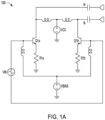
- FIG. 1A shows a simplified example, not in accordance with the claimed invention but useful for understanding the invention, of a push-pull transconductance Class A amplifier 100 circuit such as can convert a differential input voltage, Vin, into two out-of-phase output currents, Ia and Ib.
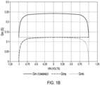
- FIG. 1B shows a corresponding graph of calculated transconductance gain (Gm, in Siemens) vs. input signal voltage amplitude (Vin, in Volts).
- the transconductance gain for each half-circuit is GMa and GMb, respectively, and the combined transconductance of the whole circuit is the sum of GMa with GMb.
- Gain-establishing or gain degeneration resistors Rla and Rlb can be connected in an emitter-follower configuration with the respective bipolar transistors Q1a and Q1b.
- the resistors R1a and R1b can serve to linearize the native transconductance of the bipolar transistors, Q1a and Q1b, respectively.
- the respective bases of the bipolar transistors Q1a and Q1b can each be coupled to a common (e.g., shared) DC bias voltage source, such as Vbias, such as via respective inductors, such as shown in FIG. 1A .
- the respective collectors of the bipolar transistors, Q1a and Q1b can each be coupled to a common (e.g., shared) DC supply bias voltage source, such as Vcc, such as via respective inductors, such as shown in FIG. 1A .
- the respective collectors of the bipolar transistors, Q1a and Q1b can each be coupled to outputs of the amplifier circuit, such as can present a capacitive differential load, such as shown in FIG. 1A .
- the gain degeneration resistance level is increased, such as using higher-valued resistances of R1a, R1b as compared to a lower gain degeneration resistance level, the overall amplifier transconductance decreases, and extends to accommodate a wider input signal range over a flatter response region.
- Gm differential transconductance gain
- the total bias current is 500 mA.
- the gain of the amplifier circuit 100 starts to fall, corresponding to increasing distortion.
- the transconductance, Gm, shapes can be flattened and widened to accommodate a broader input signal voltage range, such as by using increasing amounts of gain degeneration, which corresponds to reduced distortion of the input signal in the amplifier circuit 100.
- the reduced distortion comes at the expense of reduced signal gain.
- the amplifier circuit 100 can only provide transconductance gain within a limited range of input voltage, which is commensurate with the amount of bias current applied to the circuit.
- the circuit in FIG. 1A is differential in operation, it is not a true differential pair configuration.
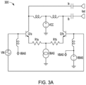
- FIG. 3A shows an example, not in accordance with the claimed invention but useful for understanding the invention, of an amplifier circuit 300 that includes such a differential pair of transistors, Q1a and Q1b, and in which the gain degeneration resistors Rla and Rlb are connected to (and bias is brought to ground through) a common (e.g., shared) current source Ibias.
- the base bias voltages of Qla and Qlb can be set to a fixed DC value (such as by respective inductors that can be coupled via respective inductors to a common (e.g., shared) bias voltage Vbias) and the common-emitter bias current of the differential pair circuit can be directly controlled by the current source Ibias.
- the gain degeneration resistors Rla and Rlb can each be fixed at 2.5 ohms.
- FIG. 3B shows an example a graph of calculated transconductance gain (Gm, in Siemens) vs. input signal voltage (Vin, in Volts) for the amplifier circuit 300 shown in FIG. 3A , for example, as Ibias is adjusted from 500 mA to 1250 mA, with these different current levels represented by respective individual curves in FIG. 3B .
- Gm differential transconductance
- Ibias input signal voltage
- gain degeneration feedback e.g., a larger input signal voltage amplitude increases the collector current through the transistor Q1a, Q1b and, in turn, through the corresponding gain degeneration resistor R1a, R1b, which decreases the base-emitter junction voltage of the corresponding transistors Q1a, Q1b, thereby tending to reduce the corresponding collector current of the particular transistor Q1a, Q1b in a negative feedback fashion
- gain degeneration feedback desensitizes the transconductance response of the transistors Q1a, Q1b for very low values of the input signal, Vin.
- FIG. 3B as the current provided by the current source Ibias is increased, the differential pair Q1a, Q1b in FIG.
- the amplitude of the input signal voltage, Vin can vary considerably with time. Moreover, in some cases, for a large percentage of time the input signal strength (e.g., amplitude) is relatively low. Unfortunately, however, the nature of some such emerging modulation schemes can cause the input signal to have large signal peaks, which can cause an amplifier to generate excessive distortion, thereby leading to what is referred to as "compression.” When an amplifier undergoes compression, information modulated onto the signal being amplified is lost-which can lead to dramatic increases in bit error rates.
- the ratio of peak signal to average signal can be referred to as the "peak-to-average" ratio, which can provide an indication of how difficult a signal can be to amplify.
- bias current provided by the bias current source Ibias in the example of FIG. 3 were increased to an appropriate level to handle the infrequent signal peaks, the power consumption and efficiency of the amplifier would suffer. On the other hand, if the bias current provided by Ibias is kept low, for good efficiency, significant bit errors can accumulate, rendering the amplifier unusable for certain applications.
- the present techniques can include, among other things, a circuit that can dynamically adjust bias current, Ibias, such as of a nominally Class A amplifier, such as a direct function of the incoming input signal, Vin, rather than as an indirect function in which the bias current of Ibias is dynamically based on an envelope of the incoming input signal, rather than on the incoming input signal itself.
- Ibias bias current
- the frequency content of the dynamically adjusted bias current, Ibias can track the frequency content of the incoming input signal, Vin, rather than tracking the arbitrary bandwidth of the envelope of the incoming input signal, Vin, as would be the case in an indirect approach.
- the bias current value of Ibias can be adjusted as a direct function of the incoming input signal, Vin, such that the dynamically variable Ibias can be used to enhance gain linearity and provide amplification with reduced distortion. This can permit the transconductance gain, such as shown in FIG. 3B , to be held nearly constant across a wider input signal range of the input signal voltage, Vin. Such adjustment can be made to correspond to an amount of bias current of Ibias needed to maintain acceptably constant or flat transconductance over much wider ranges of input signal voltage, Vin, than would be possible without the present techniques.
- FIG. 4 shows an example, not in accordance with the claimed invention but useful for understanding the invention, of an amplifier circuit 400 that can include a dynamically variable bias current source circuit, Ibias 402 that can receive the input signal, Vin.
- the dynamically variable current source, Ibias 402 can develop a suitable (e.g., non-linear) shaping function to generate the desired dynamically varying bias current of Ibias.
- the value of the bias current of Ibias 402 can be dynamically varied as a direct function of the magnitude of the input signal, Vin, such that it is capable of varying with a frequency response that can accommodate frequencies at which the input signal, Vin, varies, rather than varying indirectly, for example, as a function of an envelope of the input signal.
- the dynamically variable bias current source, Ibias 402 can include or be coupled to circuitry that can provide an offset or threshold function, such that the value of the bias current of Ibias 402 is only increased when the input signal voltage, Vin, arrives outside its otherwise useful range.
- the amplifier circuit 400 can operate in a manner similar to that illustrated in FIG. 3A and 3B , e.g., in a Class A mode with a low value of bias current provided by the dynamic bias current source Ibias 402, providing low power consumption.
- the dynamically variable bias current source 402 dynamically increase the bias currents in Qla and Qlb to extend the differential transconductance operating range, thereby avoiding or reducing compression.
- Incoming input signals with high values of peak-to-average signal voltage will rarely require adj ustments in Ibias to inhibit or prevent waveform clipping. Consequently, the net increase in average bias current is much less than otherwise would be required without using the present techniques.
- the present techniques can help increase output signal range to handle high peak-to-average signals without needing a longer duration increase in bias current.
- the dynamically variable bias current source can be configured to extend the operating range of the amplifier circuit 400.
- the direct function Ibias(Vin) will be dominated by even-order characteristics. That is, the function Ibias(Vin) will have the same result independent of the sign of Vin. That is, a large positive value of Vin will generate the same increase in the bias current provided by Ibias 402 as would the same magnitude but negative value of Vin.
- FIG. 5 shows an example, not in accordance with the claimed invention but useful for understanding the invention, of an amplifier circuit 500, similar to that shown in FIG. 4 , but including a more detailed example of a dynamically variable bias current source, Ibias 502.
- the dynamically variable bias current source Ibias 502 can include a resistor, Rbias, that is connected to and between each of the gain degeneration resistors R1a and R1b respectively associated with individual ones of the differential pair of transistors Q1a, and Q1b.
- Bias current control circuitry can include transistors Q2a, Q2b, Q3a, Q3b, and buffer or offset voltage circuits 504A, 504B.
- the buffer or offset voltage circuits 504A, 504B can perform a low impedance voltage level-shifting function on the incoming input signals provided by Vin, such as via the resistors R5a, R5b.
- the voltage signals incident to the bases of Qla and Qlb can also form the differential input to the dynamically variable bias current source circuit 502.
- the buffer or offset voltage circuits 504A, 504B can shift this input signal voltage to the dynamically variable bias current source circuit 502A, such as by a specified or predetermined amount.
- the transistors Q2a and Q2b can also provide a buffering function, such as can help inhibit or prevent loading on the bases of the transistors Qla and Qlb of the differential pair that can otherwise occur.
- the transistors Q3a and Q3b turn on, and force an increase of bias current in the transistors Qla and Qlb, such as by augmenting that current already being provided to the common-emitter differential pair circuit through the bias resistor, Rbias.
- the amplifier circuit 500 can be configured or optimized for providing an adequately wide flat region of differential transconductance, such as by adjusting the values of the offset voltage provided by the buffer or offset voltage circuits 504A, 504B. This, in turn, controls the level of input signal, Vin, needed to initiate the increase in bias current that can be dynamically provided by turning on one or both of the transistors Q3a and Q3b in parallel with the current already being provided through the bias resistor, Rbias.
- the resistance values of the resistors R2a and R2b which are respectively coupled to the emitters of Q3a, Q3b, control the ramp up in auxiliary or augmenting bias current being provided by Q3a, Q3b as the magnitude of the input signal, Vin, is increased.
- the resistors R4a and R4b can be respectively coupled between the inputs (e.g., bases) of the transistors Q1a, Q1b, of the differential pair of transistors, respectively coupling each to a common bias voltage terminal, Vbias.
- the resistance values of the resistors R4a can be respectively coupled between the inputs (e.g., bases) of the transistors Q1a, Q1b, of the differential pair of transistors, respectively coupling each to a common bias voltage terminal, Vbias.
- R4b determine the shift in voltage across the bases of the transistors Qla and Qlb of the differential pair, due to the small base currents drawn by the transistors Q2a, Q3a, Q2b, and Q3b as the transistors Q3a and Q3b turn on to dynamically adjust the auxiliary bias current being provided by Q3A, Q3b to the differential pair configuration of the transistors Qla and Qlb, augmenting the bias current being provided to the differential pair configuration of the transistors Qla and Qlb through the bias resistor Rbias.
- FIG. 6 is an example of a graph of calculated transconductance (Gm, Siemens) and bias current (mA) vs. input voltage (V), which shows a benefit of the present approach, including the dynamically variable bias current source Ibias 502 of FIG. 5 , as compared to an approach without including the dynamically variable bias current source 502 but still including the bias current resistor, Rbias.
- the dynamically variable bias current circuit Ibias 502 With the dynamically variable bias current circuit Ibias 502, a much wider range of input signal with a reasonably flat transconductance is maintained. In this example, bias current is increased only when the input voltage condition warrants additional expenditure of power. For emerging modulation schemes with high peak-to-average ratios, this increase in bias current rarely happens. This means that the increase in time-averaged bias current will be minor. However, since the trans-conductance, Gm, is maintained relatively flat across this wider range, the approach using the dynamically variable bias current circuit Ibias 502 is capable of operating with much fewer bit-errors than the approach without using the dynamically variable bias current circuit Ibias 502.
- FIG. 7 shows another example, not in accordance with the claimed invention but useful for understanding the invention, of an amplifier circuit 700 consistent with the teachings of the present approach.
- FIG. 7 shows an example of a dynamically variable bias current circuit 702, which is similar in some respects to the dynamically variable bias current circuit 502, as explained with respect to FIG. 5 .
- the dynamically variable bias current circuit 702 can include buffer circuitry, such as can include transistors Q2a, Q2b. Such buffer circuitry can help inhibit or prevent the dynamically variable bias current circuit Ibias 702 from excessively loading the inputs to the main transistors Qla, Qlb forming the input transconductors of the differential pair amplifier.
- Resistors R7a and R7b can respectively couple the inputs (e.g., base terminals) of the buffering transistors Q2a, Q2b to receive the input signal, Vin, such as to the respective inputs (e.g., base terminals) of the main transistors Q1a, Q1b.
- the collectors of the buffering transistors Q2a, Q2b can respectively be directly or indirectly electrically connected to a reference or supply voltage, such as to an upper supply voltage rail, Vcc.
- the emitters of the buffering transistors Q2a, Q2b can respectively be coupled to a reference or supply voltage, such as to a ground voltage, such as respectively through resistors R3a, R3b.
- the resistance values of the resistors R3a, R3b can be selected to keep the buffer transistors Q2a, Q2b in their forward active operating region, such as over the extended range of input voltage swing, such that any time delays associated with their operation can be kept relatively constant.
- the transistors Q4a, Q4b, Q5a, Q5b can be included such as to provide a voltage offset or to perform level-shifting.
- the transistors Q4a, Q4b, Q5a, Q5b can be diode-connected (e.g., with respective base terminals electrically connected to corresponding respective collector terminals), such as to provide the voltage offset or level-shifting.
- the series configuration of Q4a with Q5a provides a level-shifting of two forward-biased diode voltage drops, as does the series configuration of Q4b with Q5b.
- Such offset or level-shifting can help establish the magnitude of input voltage excursions that actually trigger the dynamic supplementary or auxiliary increase in bias current to the transistors Q1a, Q1b of the differential pair circuit.
- the resistance values of the resistors R6a, R6b can be selected such as to establish the nominal currents of the transistors Q4a, Q4b, Q5a, and Q5b.
- the bias currents for the differential pair of transistors Qla, Qlb, for low values of Vin can be set through Q3a, Q3b and R2a, R2b.
- the bias resistor Rbias (such as shown in FIG. 5 ) can optionally be additionally included in the example of FIG.
- a quiescent bias current can be respectively provided to the base terminals of each of the transistors Q3a, Q3b, such as by including respective bias resistors between such base terminals of the transistors Q3a, Q3b and an appropriate supply voltage (e.g., Vcc) or reference voltage (e.g., Vbias).
- Vcc supply voltage
- Vbias reference voltage
- Such biasing of Q3a, Q3b can provide appropriate quiescent currents from the collectors of Q3a, Q3b to the differential pair transistors Q1a, Q1b such as to provide operation of the differential pair transistors Q1a, Q1b in a forward-active region of operation such as for amplifying the input signal when Ibias is at its quiescent value, rather than its dynamically-boosted value.
- FIG. 8 shows another example, not in accordance with the claimed invention but useful for understanding the invention, of an amplifier circuit 700 consistent with the teachings of the present approach.
- FIG. 8 shows an example of a dynamically variable bias current circuit 802, which is similar in some respects to the dynamically variable bias current circuit 702, as explained with respect to FIG. 7 .
- the dynamically variable bias current circuit 802 can include buffer circuitry, such as can include transistors Q2a, Q2b, which in this example can be located in-line with the input signal path to the differential pair transistors Q1a, Q1b.
- FIG. 8 shows another example, not in accordance with the claimed invention but useful for understanding the invention, of an amplifier circuit 700 consistent with the teachings of the present approach.
- FIG. 8 shows an example of a dynamically variable bias current circuit 802, which is similar in some respects to the dynamically variable bias current circuit 702, as explained with respect to FIG. 7 .
- the dynamically variable bias current circuit 802 can include buffer circuitry, such as can include transistors Q2a
- FIG. 8 shows an example of a Darlington-type configuration, such as with the respective bases of the buffer transistors Q2a, Q2b receiving the input signal, Vin, and with the emitters of the buffer transistors Q2a, Q2b respectively connected to the base terminals of the differential pair transistors Q1a, Q1b.
- the collectors of the buffer transistors Q2a, Q2b can be electrically connected to a supply voltage reference, such as VCC, or alternatively to the corresponding collectors of the differential pair transistors Qla, Qlb, respectively, for biasing.
- the emitters of the buffer transistors Q2a, Q2b can be connected to a negative supply reference or ground voltage, such as through the resistors R3a, R3b, respectively.
- the offset or level shifting circuits provided by Q4a, Q5a, Q4b, Q5b can take their inputs from the emitters of Q2a and Q2b and, as in the circuit of FIG. 7 , can each operate in the forward-active region, such as can provide a consistent time response.
- FIG. 9 shows an example, not in accordance with the claimed invention but useful for understanding the invention, of an amplifier circuit 900 such as can include a dynamic bias current circuit 902, such as can include separate buffer transistors Q6a, Q6b, such as for providing in-line buffering of the differential pair transistors Q1a, Q1b.
- a separate pair of buffer transistors Q2a, Q2b can help inhibit loading by the dynamic bias current circuit 902.
- Respective delay circuits 904a, 904b can be included, such as to help balance the phase delay response of the input signal modulating the bias current via Q3a, Q3b with that of the primary signal-amplification path through the differential pair transistors Q1a, Q1b, so that the increase in bias current needed for large voltage excursions of Vin can be timely available through the differential pair transistors Q1a, Q1b when needed for amplifying the signal undergoing such large amplitude voltage excursions.
- the circuit in FIG. 9 can help overcome the challenge of aligning the input signal, Vin, to the optimum phase of the bias current being dynamically adjusted and provided to the differential pair Q1a, Q1b by the transistors Q3a, Q3b.
- the buffer transistors Q6a, Q6b can be configured in a Darlington arrangement to buffer the input signal to the differential pair transistors Q1a, Q1b.
- Separate buffer transistors Q2a, Q2b can be arranged to buffer the amplifier inputs from the circuitry of the dynamic current bias circuit 902.
- delay circuits 904a, 904b can be included in the signal path, such as after such signal inputs are received by the dynamic current bias circuit 902, and before the Darlington inputs of the buffer transistors Q6a, Q6b.
- the delay circuits 904a, 904b can include RC or LC passive low-pass filter circuits such as to help provide a desired amount of phase delay.
- the delay circuits 904a, 904b can additionally or alternatively include coaxial delay lines such as to help provide the desired amount of phase delay. This can help provide valuable flexibility, such as when applying the present approach in a narrowband application, such as can be desirable for a wireless high-power amplifier application. Shunt feedback (such as shown in FIG.
- the examples described with respect to the preceding FIGS. can convert an input voltage signal, Vin, to output currents Ia, Ib, which can form a useful building block for many practical circuit applications.
- the differential output current Iout in FIGS. 4-5 and 7-9 can be combined, such as using an impedance transformer circuit, such as can convert the high output impedance into a suitable lower impedance, such as for transmission in a broadband system such as in a cable television type communication system.
- impedance transformation can be provided by including a cascode circuit topology, an example of which is shown in FIG. 10 .
- FIG. 10 shows an example of an amplifier circuit 1000 that can include a cascode output circuit 1002 coupled to the legs of the differential pair circuit of the transistors Q1a, Q1b, such as being coupled thereto at the respective collectors of the differential pair transistors Q1a, Q1b.
- the cascode output circuit 1002 can include cascode field effect transistor (FET) or other transistors Q7a, Q7b, such as can respectively include their FET source terminals being respectively coupled to the corresponding collector terminals of the differential pair transistors Q1a, Q1b.
- FET cascode field effect transistor
- the cascode transistors Q7A, Q7b take the collector currents of the respective differential pair transistors Q1a, Q1b and convert them into a suitably high voltage, such as for transformer T2 to convert into a common impedance.
- the impedance ratio of the transformer T2 can be specified, such as to maximize or achieve a desired value of power efficiency.
- Common impedance ratios of the transformer T2 can range from 1-to-1 up to 4-to-1 with the larger impedance of the radio being applied on the cascode devices Q7a, Q7b.
- output cascode devices Q7a, Q7b should be selected or configured to be able to handle the resulting high voltage swings due to the transformer T2.
- Gallium Nitride (GaN) or other compound semiconductor FET can be well-suited for this task.
- the gate terminals of the cascode transistors Q7a, Q7b can be biased by a low current supply voltage reference, such as the bias reference voltage source Vgate shown in FIG. 10 . This can be accomplished using a biasing network within the bias reference voltage source Vgate that can include one or more resistive components, one or more Zener or other diode components, or a combination of these.
- the amplifier circuit 1000 includes a dynamic current bias circuit 902, such as can include separate buffer transistors Q2a, Q2b from the buffer transistors Q6a, Q6b used in the signal path for buffering the input signal being provided to the differential pair transistors Q1a, Q1b.
- the transistors Q4a, Q4b, Q5a, Q5b can provide the offset or level-shifting function, such as explained previously.
- Delay circuits 904a, 904b can be included, such as explained previously.
- the dynamic current source transistors Q3a, Q3b can serve to dynamically increase the bias current (e.g., as a direct function of the input signal, albeit with buffering and level-shifting), such as to help maintain constant transconductance gain for large amplitude values of the input signal, Vin.
- the input signal can be transformer-coupled into the amplifier circuit 1000, such as via the transformer Tl.
- the transformer T1 can serve to accept and transform an unbalanced input signal, Vin, into a balanced signal such as to drive the amplifier circuit 1000 differentially.
- the amplifier can provide a series-shunt feedback configuration.
- gain degeneration resistors R1a, R1b coupled to the emitters of the differential pair of transistors Q1a, Q1b provide series negative feedback for stabilizing the amplifier by tending to reduce the base-emitter voltages of the differential pair of transistors Q1a, Q1b at larger values of collector/emitter current.
- the resistors R8a, R8b and their respective series capacitors C1a, C1b can provide shunt feedback for operating the amplifier.
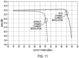
- FIG. 11 is a calculated graph of gain (in decibels, dB) vs. output power (in decibels below 1 mW, dBm) comparing the gain compression of the amplifier circuit 1000 topology shown in FIG. 10 with and without the above-described dynamic bias current modulation as a direct function of the input voltage signal.
- the gain compression performance of an amplifier is the output power where gain has dropped by a predetermined amount.
- FIG. 11 shows that using the dynamic bias current modulation can provide an increase in 1-dB compression performance of more than 8 dB.
- FIG. 12 is a graph of intercept point (decibels under 1 mW, dBm) vs. output power/tone (decibels under 1 mW, dBm) for the amplifier circuit 1000 shown in FIG. 10 , showing third-order output axis intercept point (OIP3) and fifth-order output axis intercept point (OIP5) with and without the dynamic bias current modulation circuit 902.
- OIP3 third-order output axis intercept point
- OFIP5 fifth-order output axis intercept point
- a measure of performance for a linear amplifier can be given by its output odd-order intermodulation distortion terms, such as third-order intermodulation distortion (IMD3) and fifth-order intermodulation distortion (IMD5), which are the respective ratios of power in the third-order or fifth-order distortion products, relative to the fundamental power at the fundamental frequency.
- IMD3 third-order intermodulation distortion
- IMD5 fifth-order intermodulation distortion
- IMD3 and IMD5 are strongly desirable. As input signal amplitude is increased IMD3 and IMD5 will increase. When an amplifier undergoes compression, these terms IMD3 and IMD5 can dramatically rise.
- a useful expression characterizing intermodulation performance of an amplifier is OIPx, where "x" is the order of distortion product, and is the hypothetical power level at which the IMD level equals the fundamental power. When an amplifier undergoes compression, OIP3 and OIP5 will drop dramatically, indicating that bit errors are likely to accumulate quickly. Simulated OIP3 and OIP5 for the circuit of FIG. 10 (with and without the dynamic bias current modulation) is shown in FIG. 12 . As seen in FIG.
- both OIP3 and OIP5 maintain the same or higher levels with the present dynamic bias current modulation as compared to without.
- the same topology and nominal bias current are used, with the dynamic bias current modulation providing a temporary increase in bias current for large input signal magnitudes.
- the function Ibias(Vin) can be established or optimized with a goal of reducing or minimizing both the even and odd order distortion terms of each output current Ia and Ib.
- the second order terms within the quantity Ia and Ib can be shown to cancel each other, but in practice, such cancellation is not perfect.
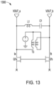
- a second order cancellation circuit is used, such as to reduce resulting second order currents, such as shown in the example of FIG. 13 .
- FIG. 13 shows an example of a cascode output stage 1300 portion of an amplifier circuit, in which a balun T3 is connected such that even-order currents within Ia and Ib will short out, rendering the outputs Vout_a and Vout_b free of second order distortions.
- a low pass filter such as formed by L1 and C1 in series with each other, with such series placed across Vout_a and Vout_b.
- This can provide a supplemental lowpass notch formed by Ll and Cl, which can help short out second order harmonics for the upper portion of the frequency band for which balun second-order attenuation performance is insufficient.
- Bias current is brought in through the balun T3. It can be noted that the direction of bias current within the balun T3 results in magnetic flux cancellation, which prevents the magnetic material from saturating.
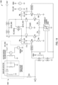
- FIG. 14 shows an example of an amplifier circuit 1400 in which an envelope tracking circuit 1402 can be additionally included, such as can additionally modulate a magnitude of supply voltage VCC used by the amplifier circuit 1400, with such envelope being an indirect function of the input signal, Vin, which does not include all the high frequency content of Vin.
- an envelope tracking circuit 1402 can be additionally included, such as can additionally modulate a magnitude of supply voltage VCC used by the amplifier circuit 1400, with such envelope being an indirect function of the input signal, Vin, which does not include all the high frequency content of Vin.
- the bias current can be dynamically adjusted as a direct function of the input signal, Vin, albeit with level-shifting, buffering, or delay, as explained earlier, such that the bias current modulation can track the high frequency content of the input signal, Vin.
- the envelope tracking circuit 1402 can adjust the supply voltage Vcc that delivers the main bias current, such as to dynamically increase the supply voltage Vcc for higher input signal envelope magnitudes, since it can be difficult to provide a voltage source able to track the full bandwidth of incoming signal. In such a case, it can be useful to determine the envelope of the incoming input signal, Vin, and use that information to adjust the primary supply, shown as VCC_High in FIG. 14 .
- the envelope detector circuit 1402 can include a series diode and shunt capacitor, resistor, and inductor components, such as shown in FIG. 14 .
- DSP digital signal processing
- Vcc envelope detector
- the present techniques can also be applied to a single-ended which is not covered by the scope of the claimed invention which is determined by the appended claims, such as can include using a half-circuit of the differential pair, or such as can include biasing an input base terminal of one of the differential pair of transistors at a fixed voltage and coupling the varying input signal to the other of the differential pair of transistors.
- Geometric terms such as “parallel”, “perpendicular”, “round”, or “square”, are not intended to require absolute mathematical precision, unless the context indicates otherwise. Instead, such geometric terms allow for variations due to manufacturing or equivalent functions. For example, if an element is described as “round” or “generally round,” a component that is not precisely circular (e.g., one that is slightly oblong or is a many-sided polygon) is still encompassed by this description.
- Method examples described herein can be machine or computer-implemented at least in part. Some examples can include a computer-readable medium or machine-readable medium encoded with instructions operable to configure an electronic device to perform methods as described in the above examples.
- An implementation of such methods can include code, such as microcode, assembly language code, a higher-level language code, or the like. Such code can include computer readable instructions for performing various methods. The code may form portions of computer program products. Further, in an example, the code can be tangibly stored on one or more volatile, non-transitory, or non-volatile tangible computer-readable media, such as during execution or at other times.
- Examples of these tangible computer-readable media can include, but are not limited to, hard disks, removable magnetic disks, removable optical disks (e.g., compact disks and digital video disks), magnetic cassettes, memory cards or sticks, random access memories (RAMs), read only memories (ROMs), and the like.
Landscapes
- Engineering & Computer Science (AREA)
- Power Engineering (AREA)
- Physics & Mathematics (AREA)
- Nonlinear Science (AREA)
- Computer Networks & Wireless Communication (AREA)
- Signal Processing (AREA)
- Amplifiers (AREA)
Claims (12)
- Eine Leistungsverstärkerschaltung (400) für Breitbanddatenkommunikation über einen Pfad in einem Kommunikationsnetz, während eine Verstärkungsleistungsfähigkeit mit geringen Verzerrungen aufrechterhalten wird, wobei die Leistungsverstärkerschaltung (400) umfasst:ein Differenzpaar eines ersten und eines zweiten Transistors (Q1a, Q1b), die mittels eines jeweiligen ersten bzw. zweiten Widerstands an einen gemeinsamen Emittervorbelastungsknoten gekoppelt sind;eine dynamische veränderliche Vorbelastungsstromschaltung (402), die an den gemeinsamen Emittervorbelastungsknoten des Differenzpaars gekoppelt ist, um einen dynamischen veränderlichen Vorbelastungsstrom als eine Funktion einer Eingangssignalamplitude eines Eingangssignals, das zum Differenzpaar des ersten und des zweiten Transistors (Q1a, Q1b) kommuniziert wird, zu ihm zu liefern;einen ersten und einen zweiten Kaskodentransistor (Q7a, Q7b), die gekoppelt sind, um jeweilige Ausgangsströme des Differenzpaars des ersten und des zweiten Transistors (Q1a, Q1b) zu empfangen;ein Balun (T3), das eine erste Wicklung und eine zweite Wicklung umfasst, wobei jede der ersten und der zweiten Wicklung jeweils einen ersten und einen zweiten Anschluss umfasst, der erste Anschluss der ersten Wicklung und der zweite Anschluss der zweiten Wicklung derart gekoppelt sind, dass die Richtung eines Vorbelastungsstroms im Balun in einer Magnetflussunterdrückung resultiert, und der zweite Anschluss der ersten Wicklung und der erste Anschluss der zweiten Wicklung an die jeweiligen Kollektoranschlüsse des Differenzpaars des ersten und des zweiten Transistors (Q1a, Q1b) jeweils mittels des ersten und des zweiten Kaskodentransistors (Q7a, Q7b) gekoppelt sind, um Oberschwingungen gerader Ordnung kurzzuschließen;einen Ausgangstransformator (T2), der an die jeweiligen Kollektoranschlüsse des Differenzpaars des ersten und des zweiten Transistors (Q1a, Q1b) gekoppelt ist, um Ausgangsströme des Differenzpaars des ersten und des zweiten Transistors (Q1a, Q1b) in eine Ausgangsspannung umzuwandeln; undein passives LC-Kerbfilter, das eine Reihenschaltung einer Spule (LT) und eines Kondensators (C1) umfasst, die zwischen jeweiligen Kollektoranschlüssen des ersten und des zweiten Kaskodentransistors (Q1a, Q1b) verbunden ist, um Oberschwingungen zweiter Ordnung kurzzuschließen.
- Die Leistungsverstärkerschaltung nach Anspruch 1, wobei die dynamische veränderliche Vorbelastungsstromschaltung (402) eingerichtet ist, den dynamischen veränderlichen Vorbelastungsstrom zum Differenzpaar des ersten und des zweiten Transistors (Q1a, Q1b) in Reaktion auf eine Zunahme der Eingangssignalamplitude zu erhöhen.
- Die Leistungsverstärkerschaltung nach Anspruch 2, wobei die dynamische veränderliche Vorbelastungsstromschaltung (402) eingerichtet ist, den dynamischen veränderlichen Vorbelastungsstrom zum Differenzpaar des ersten und des zweiten Transistors (Q1a, Q1b) mit dem vollständigen Frequenzspektralgehalt des Eingangssignals zu variieren.
- Die Leistungsverstärkerschaltung nach Anspruch 2, wobei die dynamische veränderliche Vorbelastungsstromschaltung (402) eingerichtet ist, eine Zunahme des dynamischen veränderlichen Vorbelastungsstroms zum Differenzpaar lediglich auszulösen, wenn eine Eingangssignalamplitude eine festgelegte Schwellenwertspannung überschreitet.
- Der Leistungsverstärker nach Anspruch 4, wobei die dynamische veränderliche Vorbelastungsstromschaltung (402) eine Versatzschaltung oder eine Pegelschiebeschaltung (504A, 504B) enthält, um die festgelegte Schwellenwertspannung bereitzustellen.
- Der Leistungsverstärker nach einem der Ansprüche 1 bis 5, der ferner eine Hüllkurvenverfolgungsschaltung (1402) umfasst, die eingerichtet ist, eine Versorgungsspannung des Differenzpaars des ersten und des zweiten Transistors (Q1a, Q1b) in Reaktion auf eine Hüllkurve des Eingangssignals zu variieren.
- Der Leistungsverstärker nach einem der Ansprüche 1 bis 5, der ferner Verzögerungsschaltungen (904A, 904B) auf einem Signalpfad des Eingangssignals zwischen einem Eingang des Leistungsverstärkers und jeweiligen Basen des ersten und des zweiten Transistors (Q1a, Q1b) des Differenzpaars umfasst und eingerichtet ist, eine Phase des dynamischen veränderlichen Vorbelastungsstroms auf eine Signalverstärkung des Eingangssignals durch das Differenzpaar des ersten und des zweiten Transistors (Q1a, Q1b) durch Bereitstellen einer Verzögerung auf dem Signalpfad zum Differenzpaar des ersten und des zweiten Transistors (Q1a, Q1b) auszurichten.
- Der Leistungsverstärker nach einem der Ansprüche 1 bis 5, wobei der Leistungsverstärker ferner einen Eingangstransformator (T1) umfasst, der das Eingangssignal zur Kommunikation an Eingänge des Differenzpaars des ersten und des zweiten Transistors (Q1a, Q1b) koppelt.
- Der Leistungsverstärker nach einem der Ansprüche 1 bis 5, wobei die dynamische veränderliche Vorbelastungsstromschaltung enthält:einen ersten und ein zweiten Vorbelastungsstromtransistor, die jeweils an den gemeinsamen Emittervorbelastungsknoten des Differenzpaars des ersten und des zweiten Transistors gekoppelt sind, wobei jeweilige Eingänge durch das Eingangssignal differentiell gesteuert werden; undeinen ersten und einen zweiten Vorbelastungswiderstand, die jeweils an einen entsprechenden des ersten und des zweiten Vorbelastungsstromtransistors gekoppelt sind.
- Ein Verfahren zur Leistungsverstärkung für Breitbanddatenkommunikation über einen Pfad in einem Kommunikationsnetz, während eine Verstärkungsleistungsfähigkeit mit geringen Verzerrungen aufrechterhalten wird, wobei das Verfahren Folgendes umfasst:Empfangen eines Eingangssignals;differentielles Kommunizieren des Eingangssignals zu einem ersten und einem zweiten Eingang einer Differenzverstärkerschaltung;Variieren eines dynamischen veränderlichen Vorbelastungsstroms, der zur Differenzverstärkerschaltung geliefert wird, als eine Funktion des Eingangssignals, um den dynamischen veränderlichen Vorbelastungsstrom zur Differenzverstärkerschaltung zu erhöhen;Dämpfen eines Verzerrungsprodukts gerader Ordnung einer Verstärkung des Eingangssignals unter Verwendung eines Baluns (T3), das eine erste Wicklung und eine zweite Wicklung umfasst, wobei jede der ersten und der zweiten Wicklung jeweils einen ersten und einen zweiten Anschluss umfasst und der erste Anschluss der ersten Wicklung und der zweite Anschluss der zweiten Wicklung derart gekoppelt sind, dass die Richtung eines Vorbelastungsstroms im Balun in einer Magnetflussunterdrückung resultiert;Filtern unter Verwendung eines passiven LC-Kerbfilters, das eine Reihenschaltung einer Spule (L1) und eines Kondensators (C1) umfasst, um Oberschwingungen zweiter Ordnung kurzzuschließen; undUmwandeln von Ausgangsströmen der Differenzverstärkerschaltung in eine Ausgangsspannung unter Verwendung eines Ausgangstransformators (T2).
- Das Verfahren nach Anspruch 10, wobei das Variieren des dynamischen veränderlichen Vorbelastungsstroms ein Variieren des dynamischen veränderlichen Vorbelastungsstroms, der zur Differenzverstärkerschaltung geliefert wird, als eine Funktion des Eingangssignals umfasst, um den Vorbelastungsstrom zur Differenzverstärkerschaltung zu erhöhen, wenn eine Amplitude des Eingangssignals einen festgelegten Schwellenwert überschreitet.
- Das Verfahren nach einem der Ansprüche 10 oder 11, wobei eines der Folgenden gilt:das Verfahren umfasst ferner ein Bereitstellen einer Verzögerung auf einem Signalpfad des Eingangssignals zur Differenzverstärkerschaltung, um die Phase eines Variierens des dynamischen veränderlichen Vorbelastungsstromsignals auf eine Verstärkung des Eingangssignals durch die Differenzverstärkerschaltung auszurichten; oderdas Verfahren umfasst ferner eine Verfolgung einer Hüllkurve des Eingangssignals und ein Einstellen einer Versorgungsspannung unter Verwendung der Hüllkurve des Eingangssignals.
Priority Applications (1)
| Application Number | Priority Date | Filing Date | Title |
|---|---|---|---|
| EP24161505.3A EP4358401A3 (de) | 2017-01-26 | 2018-01-25 | Aktive vorspannungsmodulationslinearisierung für breitbandverstärker |
Applications Claiming Priority (2)
| Application Number | Priority Date | Filing Date | Title |
|---|---|---|---|
| US201762450670P | 2017-01-26 | 2017-01-26 | |
| PCT/US2018/015255 WO2018140609A1 (en) | 2017-01-26 | 2018-01-25 | Bias modulation active linearization for broadband amplifiers |
Related Child Applications (2)
| Application Number | Title | Priority Date | Filing Date |
|---|---|---|---|
| EP24161505.3A Division EP4358401A3 (de) | 2017-01-26 | 2018-01-25 | Aktive vorspannungsmodulationslinearisierung für breitbandverstärker |
| EP24161505.3A Division-Into EP4358401A3 (de) | 2017-01-26 | 2018-01-25 | Aktive vorspannungsmodulationslinearisierung für breitbandverstärker |
Publications (3)
| Publication Number | Publication Date |
|---|---|
| EP3574582A1 EP3574582A1 (de) | 2019-12-04 |
| EP3574582A4 EP3574582A4 (de) | 2020-10-07 |
| EP3574582B1 true EP3574582B1 (de) | 2024-09-18 |
Family
ID=62906693
Family Applications (2)
| Application Number | Title | Priority Date | Filing Date |
|---|---|---|---|
| EP18744503.6A Active EP3574582B1 (de) | 2017-01-26 | 2018-01-25 | Aktive vorspannungsmodulationslinearisierung für breitbandverstärker |
| EP24161505.3A Withdrawn EP4358401A3 (de) | 2017-01-26 | 2018-01-25 | Aktive vorspannungsmodulationslinearisierung für breitbandverstärker |
Family Applications After (1)
| Application Number | Title | Priority Date | Filing Date |
|---|---|---|---|
| EP24161505.3A Withdrawn EP4358401A3 (de) | 2017-01-26 | 2018-01-25 | Aktive vorspannungsmodulationslinearisierung für breitbandverstärker |
Country Status (5)
| Country | Link |
|---|---|
| US (1) | US10389312B2 (de) |
| EP (2) | EP3574582B1 (de) |
| CN (1) | CN110268626B (de) |
| TW (1) | TWI653822B (de) |
| WO (1) | WO2018140609A1 (de) |
Families Citing this family (10)
| Publication number | Priority date | Publication date | Assignee | Title |
|---|---|---|---|---|
| JP2018050200A (ja) * | 2016-09-21 | 2018-03-29 | 株式会社村田製作所 | 電力増幅モジュール |
| US10476454B2 (en) | 2016-09-21 | 2019-11-12 | Murata Manufacturing Co., Ltd. | Power amplifier module |
| EP3574582B1 (de) | 2017-01-26 | 2024-09-18 | Analog Devices, Inc. | Aktive vorspannungsmodulationslinearisierung für breitbandverstärker |
| US10848109B2 (en) | 2017-01-26 | 2020-11-24 | Analog Devices, Inc. | Bias modulation active linearization for broadband amplifiers |
| US11088665B2 (en) | 2019-10-02 | 2021-08-10 | Analog Devices, Inc. | Linear broadband transconductance amplifier |
| US11264953B2 (en) * | 2020-01-31 | 2022-03-01 | Analog Devices International Unlimited Company | Bias arrangements for improving linearity of amplifiers |
| CN112953411A (zh) * | 2021-03-10 | 2021-06-11 | 西安博瑞集信电子科技有限公司 | 一种超宽带功率放大器 |
| US11843356B2 (en) * | 2021-09-21 | 2023-12-12 | Apple Inc. | Radio-frequency power amplifier with amplitude modulation to amplitude modulation (AMAM) compensation |
| CN115940832A (zh) * | 2022-11-01 | 2023-04-07 | 西安电子科技大学 | 一种应用于氮化镓Doherty功率放大器的线性化方法 |
| WO2025188440A1 (en) * | 2024-03-07 | 2025-09-12 | Qorvo Us, Inc. | Active balun |
Citations (3)
| Publication number | Priority date | Publication date | Assignee | Title |
|---|---|---|---|---|
| US6252460B1 (en) * | 1999-01-12 | 2001-06-26 | Matsushita Electric Industrial Co., Ltd. | FET balun transformer |
| US20050062533A1 (en) * | 2003-09-18 | 2005-03-24 | Vice Michael W. | Coupled-inductance differential amplifier |
| US20150130539A1 (en) * | 2013-11-13 | 2015-05-14 | Rfaxis, Inc. | Quasi-differential rf power amplifier with high level of harmonics rejection |
Family Cites Families (37)
| Publication number | Priority date | Publication date | Assignee | Title |
|---|---|---|---|---|
| US4638260A (en) | 1984-09-21 | 1987-01-20 | Hamley James P | Audio amplifier |
| US5012199A (en) | 1989-09-08 | 1991-04-30 | St. Louis Music, Inc. | Multi-stage musical instrument amplifier having distortion modes |
| US5216379A (en) * | 1992-06-26 | 1993-06-01 | Hamley James P | Dynamic bias amplifier |
| JP2661527B2 (ja) | 1993-01-27 | 1997-10-08 | 日本電気株式会社 | 差動増幅回路 |
| US5559469A (en) | 1994-03-14 | 1996-09-24 | Smith; Randall C. | Vacuum tube amplifier with selectable power devices |
| US5880632A (en) | 1994-05-09 | 1999-03-09 | Wako Technical Co., Ltd. | Tube amplifier having special configuration with two or more tubes |
| US5477188A (en) | 1994-07-14 | 1995-12-19 | Eni | Linear RF power amplifier |
| US5793252A (en) | 1995-12-12 | 1998-08-11 | Mesa Boogie, Limited | Power amplifier with switchable voicing elements |
| JPH10173456A (ja) * | 1996-12-11 | 1998-06-26 | Fujitsu Ltd | 信号増幅回路 |
| US6175279B1 (en) | 1997-12-09 | 2001-01-16 | Qualcomm Incorporated | Amplifier with adjustable bias current |
| US6615028B1 (en) | 1998-12-29 | 2003-09-02 | Skyworks Solutions, Inc. | System and method for selecting amplifiers in a communications device |
| US6218902B1 (en) | 1999-04-20 | 2001-04-17 | Nortel Networks Limited | Wide-band linearization technique |
| JP3600115B2 (ja) | 2000-04-05 | 2004-12-08 | 株式会社東芝 | 高周波回路及び通信システム |
| US6549071B1 (en) | 2000-09-12 | 2003-04-15 | Silicon Laboratories, Inc. | Power amplifier circuitry and method using an inductance coupled to power amplifier switching devices |
| US6782244B2 (en) | 2001-03-16 | 2004-08-24 | Rf Micro Devices, Inc. | Segmented power amplifier and method of control |
| EP1258731B1 (de) | 2001-04-20 | 2006-02-01 | Fuji Photo Film Co., Ltd. | Reaktiver Träger zur Bestimmung von DNA Fragmenten |
| US6614303B2 (en) * | 2001-08-17 | 2003-09-02 | Nokia Mobile Phones, Ltd. | Signal dependent current controlled amplifier and method of performing same |
| JP2004266309A (ja) | 2003-01-14 | 2004-09-24 | Matsushita Electric Ind Co Ltd | 可変利得増幅回路及び無線通信装置 |
| US7091788B2 (en) | 2003-12-03 | 2006-08-15 | Intel Corporation | Biased Darlington transistor pair, method, and system |
| US8031003B2 (en) | 2006-05-17 | 2011-10-04 | Dishop Steven M | Solid-state RF power amplifier for radio transmitters |
| US7471156B2 (en) * | 2006-09-29 | 2008-12-30 | Motorola, Inc | Amplifier containing programmable impedance for harmonic termination |
| US7576607B2 (en) | 2008-01-03 | 2009-08-18 | Samsung Electro-Mechanics | Multi-segment primary and multi-turn secondary transformer for power amplifier systems |
| US7728661B2 (en) | 2008-05-05 | 2010-06-01 | Javelin Semiconductor, Inc. | Controlling power with an output network |
| WO2010045597A1 (en) | 2008-10-17 | 2010-04-22 | Triquint Semiconductor, Inc. | Apparatus and method for broadband amplifier linearization |
| US7768350B2 (en) | 2008-12-30 | 2010-08-03 | Javelin Semiconductor, Inc. | Output gain stage for a power amplifier |
| US8666340B2 (en) | 2009-03-03 | 2014-03-04 | Broadcom Corporation | Method and system for on-chip impedance control to impedance match a configurable front end |
| US8198968B2 (en) | 2010-09-30 | 2012-06-12 | Fujitsu Semiconductor Limited | System and method for multiple band transmission |
| US8319556B2 (en) * | 2010-11-09 | 2012-11-27 | Raytheon Company | Transformer coupled distributed amplifier |
| US8718580B2 (en) | 2011-11-11 | 2014-05-06 | Hbc Solutions, Inc. | Broadband high efficiency amplifier system incorporating dynamic modulation of load impedance |
| US8604879B2 (en) | 2012-03-30 | 2013-12-10 | Integrated Device Technology Inc. | Matched feedback amplifier with improved linearity |
| EP2713507B1 (de) | 2012-10-01 | 2014-12-10 | Nxp B.V. | FET-RF-Leistungsdetektor |
| CN103326682A (zh) * | 2013-05-27 | 2013-09-25 | 苏州贝克微电子有限公司 | 具有高线性度的可调运算跨导放大器 |
| US9231537B1 (en) * | 2014-02-11 | 2016-01-05 | M/A-Com Technology Solutions Holdings, Inc. | High power and high linearity cascode amplifier |
| JP6503663B2 (ja) | 2014-09-10 | 2019-04-24 | 住友電気工業株式会社 | 差動増幅回路 |
| WO2017160747A1 (en) | 2016-03-14 | 2017-09-21 | Day Chris J | Active linearization for broadband amplifiers |
| US10187022B2 (en) * | 2016-05-09 | 2019-01-22 | Arris Enterprises Llc | RF class AB cascode amplifier with linearization and steering diodes |
| EP3574582B1 (de) | 2017-01-26 | 2024-09-18 | Analog Devices, Inc. | Aktive vorspannungsmodulationslinearisierung für breitbandverstärker |
-
2018
- 2018-01-25 EP EP18744503.6A patent/EP3574582B1/de active Active
- 2018-01-25 WO PCT/US2018/015255 patent/WO2018140609A1/en not_active Ceased
- 2018-01-25 EP EP24161505.3A patent/EP4358401A3/de not_active Withdrawn
- 2018-01-25 US US15/879,947 patent/US10389312B2/en active Active
- 2018-01-25 CN CN201880008636.7A patent/CN110268626B/zh active Active
- 2018-01-26 TW TW107102939A patent/TWI653822B/zh active
Patent Citations (3)
| Publication number | Priority date | Publication date | Assignee | Title |
|---|---|---|---|---|
| US6252460B1 (en) * | 1999-01-12 | 2001-06-26 | Matsushita Electric Industrial Co., Ltd. | FET balun transformer |
| US20050062533A1 (en) * | 2003-09-18 | 2005-03-24 | Vice Michael W. | Coupled-inductance differential amplifier |
| US20150130539A1 (en) * | 2013-11-13 | 2015-05-14 | Rfaxis, Inc. | Quasi-differential rf power amplifier with high level of harmonics rejection |
Non-Patent Citations (1)
| Title |
|---|
| CHANG WEI-LING ET AL: "5-6 GHz CMOS low-noise direct conversion receiver using a differential RF VGA with a differential inductor load", 2016 IEEE INTERNATIONAL SYMPOSIUM ON RADIO-FREQUENCY INTEGRATION TECHNOLOGY (RFIT), IEEE, 24 August 2016 (2016-08-24), pages 1 - 3, XP032971163, DOI: 10.1109/RFIT.2016.7578129 * |
Also Published As
| Publication number | Publication date |
|---|---|
| EP4358401A2 (de) | 2024-04-24 |
| TWI653822B (zh) | 2019-03-11 |
| CN110268626B (zh) | 2023-07-18 |
| WO2018140609A1 (en) | 2018-08-02 |
| EP3574582A4 (de) | 2020-10-07 |
| EP3574582A1 (de) | 2019-12-04 |
| CN110268626A (zh) | 2019-09-20 |
| TW201841467A (zh) | 2018-11-16 |
| US10389312B2 (en) | 2019-08-20 |
| EP4358401A3 (de) | 2024-07-10 |
| US20180212573A1 (en) | 2018-07-26 |
Similar Documents
| Publication | Publication Date | Title |
|---|---|---|
| EP3574582B1 (de) | Aktive vorspannungsmodulationslinearisierung für breitbandverstärker | |
| US10848109B2 (en) | Bias modulation active linearization for broadband amplifiers | |
| US6784740B1 (en) | Power amplifier | |
| US6930549B2 (en) | Variable gain amplifier for use in communications | |
| US8107901B2 (en) | Feedback loop with adjustable bandwidth | |
| CN109314496B (zh) | 用于宽带放大器的有源线性化 | |
| US8618879B2 (en) | Semiconductor device | |
| WO2002060052A2 (en) | Precision automatic gain control circuit | |
| US8665027B2 (en) | Amplifier for wireless receiver and associated method | |
| US20030148792A1 (en) | Wideband error amplifier | |
| US6188282B1 (en) | Differential amplifier with reduced even order non-linearity and associated methods | |
| CN113508526B (zh) | 用于优化共源共栅放大器中三阶截取点的晶体管偏置调整 | |
| EP1524763A1 (de) | Modulationsabhängige Arbeitspunkteinstellung für effiziente und hochlineare Leistungsverstärker | |
| KR100856131B1 (ko) | 가변 게인 저잡음 증폭기 회로 및 이를 구비하는 무선 통신수신기 | |
| US10348260B2 (en) | Amplifier circuit and filter | |
| US20040095192A1 (en) | Radio frequency power amplifier adaptive bias control circuit | |
| US6388525B1 (en) | Amplifier with controllable variable signal gain | |
| US7454179B1 (en) | Radio frequency power detector and decision circuit used with DC supply voltage controlled power amplifiers | |
| KR20160096288A (ko) | 스퓨리어스 및 수신 밴드 잡음을 감소시키는 포락선 모듈레이터 및 이를 구비한 포락선 추적 전력 증폭장치 | |
| EP1349268B1 (de) | Variabler OS-Verstärker | |
| US7332963B2 (en) | Low noise amplifier | |
| US7474155B2 (en) | Power amplifier | |
| US7253689B2 (en) | Low distortion amplifier | |
| US20050063477A1 (en) | Transmitter/receiver for bidirectional communications | |
| JP2013081090A (ja) | 電力増幅回路、および無線通信装置 |
Legal Events
| Date | Code | Title | Description |
|---|---|---|---|
| STAA | Information on the status of an ep patent application or granted ep patent |
Free format text: STATUS: THE INTERNATIONAL PUBLICATION HAS BEEN MADE |
|
| PUAI | Public reference made under article 153(3) epc to a published international application that has entered the european phase |
Free format text: ORIGINAL CODE: 0009012 |
|
| STAA | Information on the status of an ep patent application or granted ep patent |
Free format text: STATUS: REQUEST FOR EXAMINATION WAS MADE |
|
| 17P | Request for examination filed |
Effective date: 20190801 |
|
| AK | Designated contracting states |
Kind code of ref document: A1 Designated state(s): AL AT BE BG CH CY CZ DE DK EE ES FI FR GB GR HR HU IE IS IT LI LT LU LV MC MK MT NL NO PL PT RO RS SE SI SK SM TR |
|
| AX | Request for extension of the european patent |
Extension state: BA ME |
|
| DAV | Request for validation of the european patent (deleted) | ||
| DAX | Request for extension of the european patent (deleted) | ||
| A4 | Supplementary search report drawn up and despatched |
Effective date: 20200908 |
|
| RIC1 | Information provided on ipc code assigned before grant |
Ipc: H03F 1/22 20060101ALI20200902BHEP Ipc: H03F 3/21 20060101ALI20200902BHEP Ipc: H03F 3/45 20060101AFI20200902BHEP Ipc: H03F 1/32 20060101ALI20200902BHEP Ipc: H03F 1/02 20060101ALI20200902BHEP Ipc: H03F 3/19 20060101ALI20200902BHEP |
|
| RAP3 | Party data changed (applicant data changed or rights of an application transferred) |
Owner name: ANALOG DEVICES, INC. |
|
| STAA | Information on the status of an ep patent application or granted ep patent |
Free format text: STATUS: EXAMINATION IS IN PROGRESS |
|
| 17Q | First examination report despatched |
Effective date: 20220121 |
|
| GRAP | Despatch of communication of intention to grant a patent |
Free format text: ORIGINAL CODE: EPIDOSNIGR1 |
|
| STAA | Information on the status of an ep patent application or granted ep patent |
Free format text: STATUS: GRANT OF PATENT IS INTENDED |
|
| INTG | Intention to grant announced |
Effective date: 20240215 |
|
| GRAJ | Information related to disapproval of communication of intention to grant by the applicant or resumption of examination proceedings by the epo deleted |
Free format text: ORIGINAL CODE: EPIDOSDIGR1 |
|
| STAA | Information on the status of an ep patent application or granted ep patent |
Free format text: STATUS: EXAMINATION IS IN PROGRESS |
|
| GRAP | Despatch of communication of intention to grant a patent |
Free format text: ORIGINAL CODE: EPIDOSNIGR1 |
|
| STAA | Information on the status of an ep patent application or granted ep patent |
Free format text: STATUS: GRANT OF PATENT IS INTENDED |
|
| INTC | Intention to grant announced (deleted) | ||
| INTG | Intention to grant announced |
Effective date: 20240415 |
|
| GRAS | Grant fee paid |
Free format text: ORIGINAL CODE: EPIDOSNIGR3 |
|
| GRAA | (expected) grant |
Free format text: ORIGINAL CODE: 0009210 |
|
| STAA | Information on the status of an ep patent application or granted ep patent |
Free format text: STATUS: THE PATENT HAS BEEN GRANTED |
|
| AK | Designated contracting states |
Kind code of ref document: B1 Designated state(s): AL AT BE BG CH CY CZ DE DK EE ES FI FR GB GR HR HU IE IS IT LI LT LU LV MC MK MT NL NO PL PT RO RS SE SI SK SM TR |
|
| REG | Reference to a national code |
Ref country code: GB Ref legal event code: FG4D |
|
| REG | Reference to a national code |
Ref country code: CH Ref legal event code: EP |
|
| REG | Reference to a national code |
Ref country code: DE Ref legal event code: R096 Ref document number: 602018074499 Country of ref document: DE |
|
| REG | Reference to a national code |
Ref country code: IE Ref legal event code: FG4D |
|
| REG | Reference to a national code |
Ref country code: LT Ref legal event code: MG9D |
|
| PG25 | Lapsed in a contracting state [announced via postgrant information from national office to epo] |
Ref country code: NO Free format text: LAPSE BECAUSE OF FAILURE TO SUBMIT A TRANSLATION OF THE DESCRIPTION OR TO PAY THE FEE WITHIN THE PRESCRIBED TIME-LIMIT Effective date: 20241218 |
|
| PG25 | Lapsed in a contracting state [announced via postgrant information from national office to epo] |
Ref country code: GR Free format text: LAPSE BECAUSE OF FAILURE TO SUBMIT A TRANSLATION OF THE DESCRIPTION OR TO PAY THE FEE WITHIN THE PRESCRIBED TIME-LIMIT Effective date: 20241219 Ref country code: FI Free format text: LAPSE BECAUSE OF FAILURE TO SUBMIT A TRANSLATION OF THE DESCRIPTION OR TO PAY THE FEE WITHIN THE PRESCRIBED TIME-LIMIT Effective date: 20240918 |
|
| PG25 | Lapsed in a contracting state [announced via postgrant information from national office to epo] |
Ref country code: BG Free format text: LAPSE BECAUSE OF FAILURE TO SUBMIT A TRANSLATION OF THE DESCRIPTION OR TO PAY THE FEE WITHIN THE PRESCRIBED TIME-LIMIT Effective date: 20240918 |
|
| PG25 | Lapsed in a contracting state [announced via postgrant information from national office to epo] |
Ref country code: LV Free format text: LAPSE BECAUSE OF FAILURE TO SUBMIT A TRANSLATION OF THE DESCRIPTION OR TO PAY THE FEE WITHIN THE PRESCRIBED TIME-LIMIT Effective date: 20240918 |
|
| PG25 | Lapsed in a contracting state [announced via postgrant information from national office to epo] |
Ref country code: HR Free format text: LAPSE BECAUSE OF FAILURE TO SUBMIT A TRANSLATION OF THE DESCRIPTION OR TO PAY THE FEE WITHIN THE PRESCRIBED TIME-LIMIT Effective date: 20240918 |
|
| REG | Reference to a national code |
Ref country code: NL Ref legal event code: MP Effective date: 20240918 |
|
| PG25 | Lapsed in a contracting state [announced via postgrant information from national office to epo] |
Ref country code: RS Free format text: LAPSE BECAUSE OF FAILURE TO SUBMIT A TRANSLATION OF THE DESCRIPTION OR TO PAY THE FEE WITHIN THE PRESCRIBED TIME-LIMIT Effective date: 20241218 |
|
| PG25 | Lapsed in a contracting state [announced via postgrant information from national office to epo] |
Ref country code: RS Free format text: LAPSE BECAUSE OF FAILURE TO SUBMIT A TRANSLATION OF THE DESCRIPTION OR TO PAY THE FEE WITHIN THE PRESCRIBED TIME-LIMIT Effective date: 20241218 Ref country code: NO Free format text: LAPSE BECAUSE OF FAILURE TO SUBMIT A TRANSLATION OF THE DESCRIPTION OR TO PAY THE FEE WITHIN THE PRESCRIBED TIME-LIMIT Effective date: 20241218 Ref country code: LV Free format text: LAPSE BECAUSE OF FAILURE TO SUBMIT A TRANSLATION OF THE DESCRIPTION OR TO PAY THE FEE WITHIN THE PRESCRIBED TIME-LIMIT Effective date: 20240918 Ref country code: HR Free format text: LAPSE BECAUSE OF FAILURE TO SUBMIT A TRANSLATION OF THE DESCRIPTION OR TO PAY THE FEE WITHIN THE PRESCRIBED TIME-LIMIT Effective date: 20240918 Ref country code: GR Free format text: LAPSE BECAUSE OF FAILURE TO SUBMIT A TRANSLATION OF THE DESCRIPTION OR TO PAY THE FEE WITHIN THE PRESCRIBED TIME-LIMIT Effective date: 20241219 Ref country code: FI Free format text: LAPSE BECAUSE OF FAILURE TO SUBMIT A TRANSLATION OF THE DESCRIPTION OR TO PAY THE FEE WITHIN THE PRESCRIBED TIME-LIMIT Effective date: 20240918 Ref country code: BG Free format text: LAPSE BECAUSE OF FAILURE TO SUBMIT A TRANSLATION OF THE DESCRIPTION OR TO PAY THE FEE WITHIN THE PRESCRIBED TIME-LIMIT Effective date: 20240918 |
|
| REG | Reference to a national code |
Ref country code: AT Ref legal event code: MK05 Ref document number: 1725533 Country of ref document: AT Kind code of ref document: T Effective date: 20240918 |
|
| PG25 | Lapsed in a contracting state [announced via postgrant information from national office to epo] |
Ref country code: NL Free format text: LAPSE BECAUSE OF FAILURE TO SUBMIT A TRANSLATION OF THE DESCRIPTION OR TO PAY THE FEE WITHIN THE PRESCRIBED TIME-LIMIT Effective date: 20240918 |
|
| PG25 | Lapsed in a contracting state [announced via postgrant information from national office to epo] |
Ref country code: PT Free format text: LAPSE BECAUSE OF FAILURE TO SUBMIT A TRANSLATION OF THE DESCRIPTION OR TO PAY THE FEE WITHIN THE PRESCRIBED TIME-LIMIT Effective date: 20250120 Ref country code: IS Free format text: LAPSE BECAUSE OF FAILURE TO SUBMIT A TRANSLATION OF THE DESCRIPTION OR TO PAY THE FEE WITHIN THE PRESCRIBED TIME-LIMIT Effective date: 20250118 |
|
| PG25 | Lapsed in a contracting state [announced via postgrant information from national office to epo] |
Ref country code: RO Free format text: LAPSE BECAUSE OF FAILURE TO SUBMIT A TRANSLATION OF THE DESCRIPTION OR TO PAY THE FEE WITHIN THE PRESCRIBED TIME-LIMIT Effective date: 20240918 Ref country code: SM Free format text: LAPSE BECAUSE OF FAILURE TO SUBMIT A TRANSLATION OF THE DESCRIPTION OR TO PAY THE FEE WITHIN THE PRESCRIBED TIME-LIMIT Effective date: 20240918 |
|
| PG25 | Lapsed in a contracting state [announced via postgrant information from national office to epo] |
Ref country code: ES Free format text: LAPSE BECAUSE OF FAILURE TO SUBMIT A TRANSLATION OF THE DESCRIPTION OR TO PAY THE FEE WITHIN THE PRESCRIBED TIME-LIMIT Effective date: 20240918 |
|
| PG25 | Lapsed in a contracting state [announced via postgrant information from national office to epo] |
Ref country code: AT Free format text: LAPSE BECAUSE OF FAILURE TO SUBMIT A TRANSLATION OF THE DESCRIPTION OR TO PAY THE FEE WITHIN THE PRESCRIBED TIME-LIMIT Effective date: 20240918 Ref country code: EE Free format text: LAPSE BECAUSE OF FAILURE TO SUBMIT A TRANSLATION OF THE DESCRIPTION OR TO PAY THE FEE WITHIN THE PRESCRIBED TIME-LIMIT Effective date: 20240918 |
|
| PG25 | Lapsed in a contracting state [announced via postgrant information from national office to epo] |
Ref country code: CZ Free format text: LAPSE BECAUSE OF FAILURE TO SUBMIT A TRANSLATION OF THE DESCRIPTION OR TO PAY THE FEE WITHIN THE PRESCRIBED TIME-LIMIT Effective date: 20240918 Ref country code: PL Free format text: LAPSE BECAUSE OF FAILURE TO SUBMIT A TRANSLATION OF THE DESCRIPTION OR TO PAY THE FEE WITHIN THE PRESCRIBED TIME-LIMIT Effective date: 20240918 |
|
| PG25 | Lapsed in a contracting state [announced via postgrant information from national office to epo] |
Ref country code: IT Free format text: LAPSE BECAUSE OF FAILURE TO SUBMIT A TRANSLATION OF THE DESCRIPTION OR TO PAY THE FEE WITHIN THE PRESCRIBED TIME-LIMIT Effective date: 20240918 Ref country code: SK Free format text: LAPSE BECAUSE OF FAILURE TO SUBMIT A TRANSLATION OF THE DESCRIPTION OR TO PAY THE FEE WITHIN THE PRESCRIBED TIME-LIMIT Effective date: 20240918 |
|
| REG | Reference to a national code |
Ref country code: DE Ref legal event code: R097 Ref document number: 602018074499 Country of ref document: DE |
|
| PG25 | Lapsed in a contracting state [announced via postgrant information from national office to epo] |
Ref country code: DK Free format text: LAPSE BECAUSE OF FAILURE TO SUBMIT A TRANSLATION OF THE DESCRIPTION OR TO PAY THE FEE WITHIN THE PRESCRIBED TIME-LIMIT Effective date: 20240918 |
|
| PLBE | No opposition filed within time limit |
Free format text: ORIGINAL CODE: 0009261 |
|
| STAA | Information on the status of an ep patent application or granted ep patent |
Free format text: STATUS: NO OPPOSITION FILED WITHIN TIME LIMIT |
|
| 26N | No opposition filed |
Effective date: 20250619 |
|
| REG | Reference to a national code |
Ref country code: CH Ref legal event code: PL |
|
| PG25 | Lapsed in a contracting state [announced via postgrant information from national office to epo] |
Ref country code: SE Free format text: LAPSE BECAUSE OF FAILURE TO SUBMIT A TRANSLATION OF THE DESCRIPTION OR TO PAY THE FEE WITHIN THE PRESCRIBED TIME-LIMIT Effective date: 20240918 |
|
| PG25 | Lapsed in a contracting state [announced via postgrant information from national office to epo] |
Ref country code: LU Free format text: LAPSE BECAUSE OF NON-PAYMENT OF DUE FEES Effective date: 20250125 Ref country code: MC Free format text: LAPSE BECAUSE OF FAILURE TO SUBMIT A TRANSLATION OF THE DESCRIPTION OR TO PAY THE FEE WITHIN THE PRESCRIBED TIME-LIMIT Effective date: 20240918 |
|
| GBPC | Gb: european patent ceased through non-payment of renewal fee |
Effective date: 20250125 |
|
| PG25 | Lapsed in a contracting state [announced via postgrant information from national office to epo] |
Ref country code: BE Free format text: LAPSE BECAUSE OF NON-PAYMENT OF DUE FEES Effective date: 20250131 Ref country code: GB Free format text: LAPSE BECAUSE OF NON-PAYMENT OF DUE FEES Effective date: 20250125 |
|
| PG25 | Lapsed in a contracting state [announced via postgrant information from national office to epo] |
Ref country code: FR Free format text: LAPSE BECAUSE OF NON-PAYMENT OF DUE FEES Effective date: 20250131 |
|
| PG25 | Lapsed in a contracting state [announced via postgrant information from national office to epo] |
Ref country code: CH Free format text: LAPSE BECAUSE OF NON-PAYMENT OF DUE FEES Effective date: 20250131 |
|
| REG | Reference to a national code |
Ref country code: BE Ref legal event code: MM Effective date: 20250131 |
|
| PG25 | Lapsed in a contracting state [announced via postgrant information from national office to epo] |
Ref country code: IE Free format text: LAPSE BECAUSE OF NON-PAYMENT OF DUE FEES Effective date: 20250125 |
|
| PGFP | Annual fee paid to national office [announced via postgrant information from national office to epo] |
Ref country code: DE Payment date: 20251217 Year of fee payment: 9 |