EP3574585B1 - Compensation par ajustement de seuil de bruit optique asymétrique - Google Patents
Compensation par ajustement de seuil de bruit optique asymétrique Download PDFInfo
- Publication number
- EP3574585B1 EP3574585B1 EP18751499.7A EP18751499A EP3574585B1 EP 3574585 B1 EP3574585 B1 EP 3574585B1 EP 18751499 A EP18751499 A EP 18751499A EP 3574585 B1 EP3574585 B1 EP 3574585B1
- Authority
- EP
- European Patent Office
- Prior art keywords
- circuit
- dac
- electrical
- coupled
- data
- Prior art date
- Legal status (The legal status is an assumption and is not a legal conclusion. Google has not performed a legal analysis and makes no representation as to the accuracy of the status listed.)
- Active
Links
Images


Classifications
-
- H—ELECTRICITY
- H04—ELECTRIC COMMUNICATION TECHNIQUE
- H04B—TRANSMISSION
- H04B10/00—Transmission systems employing electromagnetic waves other than radio-waves, e.g. infrared, visible or ultraviolet light, or employing corpuscular radiation, e.g. quantum communication
- H04B10/25—Arrangements specific to fibre transmission
- H04B10/2507—Arrangements specific to fibre transmission for the reduction or elimination of distortion or dispersion
-
- H—ELECTRICITY
- H03—ELECTRONIC CIRCUITRY
- H03M—CODING; DECODING; CODE CONVERSION IN GENERAL
- H03M1/00—Analogue/digital conversion; Digital/analogue conversion
- H03M1/06—Continuously compensating for, or preventing, undesired influence of physical parameters
- H03M1/08—Continuously compensating for, or preventing, undesired influence of physical parameters of noise
-
- H—ELECTRICITY
- H04—ELECTRIC COMMUNICATION TECHNIQUE
- H04B—TRANSMISSION
- H04B10/00—Transmission systems employing electromagnetic waves other than radio-waves, e.g. infrared, visible or ultraviolet light, or employing corpuscular radiation, e.g. quantum communication
- H04B10/60—Receivers
- H04B10/66—Non-coherent receivers, e.g. using direct detection
- H04B10/69—Electrical arrangements in the receiver
- H04B10/695—Arrangements for optimizing the decision element in the receiver, e.g. by using automatic threshold control
-
- H—ELECTRICITY
- H03—ELECTRONIC CIRCUITRY
- H03L—AUTOMATIC CONTROL, STARTING, SYNCHRONISATION OR STABILISATION OF GENERATORS OF ELECTRONIC OSCILLATIONS OR PULSES
- H03L7/00—Automatic control of frequency or phase; Synchronisation
- H03L7/06—Automatic control of frequency or phase; Synchronisation using a reference signal applied to a frequency- or phase-locked loop
- H03L7/08—Details of the phase-locked loop
- H03L7/0807—Details of the phase-locked loop concerning mainly a recovery circuit for the reference signal
-
- H—ELECTRICITY
- H03—ELECTRONIC CIRCUITRY
- H03M—CODING; DECODING; CODE CONVERSION IN GENERAL
- H03M3/00—Conversion of analogue values to or from differential modulation
- H03M3/04—Differential modulation with several bits, e.g. differential pulse code modulation [DPCM]
-
- H—ELECTRICITY
- H04—ELECTRIC COMMUNICATION TECHNIQUE
- H04B—TRANSMISSION
- H04B10/00—Transmission systems employing electromagnetic waves other than radio-waves, e.g. infrared, visible or ultraviolet light, or employing corpuscular radiation, e.g. quantum communication
- H04B10/25—Arrangements specific to fibre transmission
- H04B10/2589—Bidirectional transmission
- H04B10/25891—Transmission components
-
- H—ELECTRICITY
- H04—ELECTRIC COMMUNICATION TECHNIQUE
- H04B—TRANSMISSION
- H04B10/00—Transmission systems employing electromagnetic waves other than radio-waves, e.g. infrared, visible or ultraviolet light, or employing corpuscular radiation, e.g. quantum communication
- H04B10/60—Receivers
- H04B10/66—Non-coherent receivers, e.g. using direct detection
- H04B10/69—Electrical arrangements in the receiver
- H04B10/697—Arrangements for reducing noise and distortion
-
- H—ELECTRICITY
- H04—ELECTRIC COMMUNICATION TECHNIQUE
- H04B—TRANSMISSION
- H04B3/00—Line transmission systems
- H04B3/02—Details
- H04B3/04—Control of transmission; Equalising
Definitions
- the present disclosure is related to an optical-to-electrical circuit, and in particular to adjusting a threshold voltage of an output of the optical-to-electrical circuit.
- optical noise is typically asymmetrical.
- an optical "1" bit typically contains more noise than an optical "0" bit.
- the noise asymmetry results in an eye height of a differential "1” bit that is smaller than an eye height of a differential "0” bit. This may result in a higher bit error rate (BER) for the differential "1" bit as compared to the differential "0" bit. It is desirable to adjust the zero-crossing points of the incoming data in order to balance these eye heights of the differential bits.
- BER bit error rate
- US2008/0152358 A1 discloses a light receiver has a photoelectric conversion circuit which converts an input optical signal into an electrical signal, an electric amplifier which amplifies the electrical signal output from the photoelectric conversion circuit, a threshold adjustment circuit which outputs a threshold value according to signal information in the optical signal, and an optical signal loss detection circuit which compares amplitude of the electric signal output from the electric amplifier with the threshold value output from the threshold adjustment circuit and outputs results of the comparison.
- WO 2013/042175 A1 discloses a method for controlling an optical transmitter according to an exemplary aspect of the invention includes: generating a multilevel electrical signal by means of combining two or more binary electrical signals, where said multilevel signal is used to drive the modulator of adding a low frequency dither signal on several of the binary electrical signals, wherein the phase of the added dither signal depends on the value of the binary signal to which it is added; tapping a portion of light after the modulator and generating a monitor signal from the tapped light; controlling the modulator according to the monitor signal.
- US 2005062530 A1 discloses a variable decision threshold apparatus includes a comparator for receiving the electrical signal and for comparing it to a threshold level.
- a signal strength monitor monitors the strength of the electrical signal and a scaler scales the decision threshold level to the measured amplitude of the electrical signal so that the percentage set as the threshold level is maintained.
- an optical data circuit includes an optical-to-electrical conversion circuit configured to produce first and second differential electrical data signals, at respective first and second electrical nodes, in response to an optical data signal.
- a first digital-to-analog converter (DAC) circuit is coupled to the first electrical node and configured to generate a first adjustment signal.
- a second DAC circuit is coupled to the second electrical node and configured to generate a second adjustment signal, wherein the first and second DAC circuits are configured to adjust the first and second differential electrical data signals such that a zero-crossing point of positive data is pulled up in response to the first adjustment signal and a zero-crossing point of negative data is pulled down in response to the second adjustment signal.
- an optical communication system in another example, includes an optical-to-electrical conversion circuit configured to produce first and second differential electrical data signals, at respective first and second electrical nodes, in response to a single-ended optical data signal.
- a termination circuit is coupled to the first and second electrical nodes.
- a first digital-to-analog converter (DAC) circuit is coupled to the first electrical node, the first DAC circuit comprising a first binary input and a first voltage output.
- a second DAC circuit is coupled to the second electrical node, the second DAC circuit comprising a second binary input and a second voltage output.
- a linear equalizer circuit is coupled to the termination circuit and the first and second DAC circuits, wherein the first and second DAC circuits are configured to adjust the first and second differential electrical data signals based on the respective first and second voltage outputs such that a zero-crossing point of positive data is pulled up and a zero-crossing point of negative data is pulled down.
- a method for threshold adjustment compensation of optical noise when generating electrical data signals from an optical data signal includes converting the optical data signal to first and second differential electrical data signals.
- First and second threshold adjust signals are converted based on a default code and circuit characteristics.
- a zero-crossing point of the first and second differential data signals is adjusted based on the respective first and second threshold adjust signals such that the zero-crossing point of positive data is pulled up and the zero-crossing point of negative data is pulled down.
- the first and second differential data signals are equalized after the zero-crossing points of each signal has been adjusted to generate the electrical data signals.
- the zero-crossing points of the differential data may be adjusted by using differential current DACs that bias relatively small (e.g., 50 Ohm) termination resistors. Due to the relatively small termination resistors, a relatively large current (e.g., 6 mA) is necessary to achieve a desirable 300 mV pp threshold adjustment. If additional threshold adjustment is necessary, an even larger current is used. Unfortunately, this high power consumption is not acceptable in a new generation of optical modules.
- relatively small termination resistors Due to the relatively small termination resistors, a relatively large current (e.g., 6 mA) is necessary to achieve a desirable 300 mV pp threshold adjustment. If additional threshold adjustment is necessary, an even larger current is used. Unfortunately, this high power consumption is not acceptable in a new generation of optical modules.
- the disclosed embodiments use two substantially identical voltagemode DAC circuits (e.g., R-2R DAC) at an optical receiver front end.
- Each DAC circuit is coupled to a respective differential input node.
- the DAC circuits may generate adjustment signals to set the positive and negative inputs of a linear equalizer circuit to different zero-crossing points. For example, the zero-crossing point of positive data may be pulled up while the zero-crossing point of negative data may be pulled down.
- two internal alternating current (AC) coupling capacitances may be inserted between termination resistors and the linear equalizer circuit.
- two relatively high value resistances may be inserted between internal AC coupling capacitances and the DACs in order to reduce the signal direct current (DC) wandering due to limited internal AC coupling capacitance.
- the dissipated current can be reduced to less than 1 mA while decreasing the bit error rate for optical data.
- FIG. 1 is a block diagram of an optical data circuit having a threshold adjustment circuit to compensate for asymmetrical optical noise, according to example embodiments.
- the circuit includes an optical-to-electrical conversion circuit 101, a termination circuit 103, a threshold adjustment circuit 105, a threshold adjustment control circuit 109, and a linear equalizer circuit 107.
- the optical-to-electrical conversion circuit 101 includes a single-ended optical fiber input and first and second differential electrical nodes P1 and N1.
- the optical-to-electrical conversion circuit 101 may comprise any means to generate differential electrical signals in response to the optical input.
- the optical-to-electrical conversion circuit 101 may comprise a photo diode to generate electrical signals from light signals.
- the optical-to-electrical conversion circuit 101 provides differential output signals on nodes P1 and N1.
- the termination circuit 103 is coupled to the P1 and N1 nodes to pull the nodes up to a termination voltage V TERM (e.g., 3V to 5V), as illustrated in FIG. 2 .
- V TERM e.g., 3V to 5V
- the termination circuit 103 provides the terminated differential output signals on nodes P2 and N2 that are coupled to respective V INP and V INM input nodes of the linear equalizer circuit 107.
- Linear equalizer circuit 107 provides equalization to the differential input signals on respective P2 and N2 input nodes. The equalization reverses the distortion incurred by a signal transmitted through an optical channel and balances the differential electrical signals. The linear equalizer circuit 107 renders the frequency response of the differential signals flat from end-to-end. When a channel has been equalized, the frequency domain attributes of the signal at the input are faithfully reproduced at the output. The linear equalizer circuit 107 also cancels out any group delay and phase delay between different frequency components.
- the threshold adjustment circuit 105 is coupled to the P2 and N2 nodes of the termination circuit 103.
- a threshold adjustment control circuit 109 may be coupled to the threshold adjustment circuit 105 or may be part of the threshold adjustment circuit 105.
- the threshold adjustment control circuit 109 provides select control words SELM and SELP to the DACs of the threshold adjustment circuit 105 as described subsequently in greater detail.
- the optical-to-electrical conversion circuit 101 accepts a single-ended optical data signal from the optical input and converts the light signal to a representative electrical data signal (e.g., voltage signal). In the illustrated embodiment, the optical-to-electrical conversion circuit 101 converts the optical signal to differential output voltages on the P1 and N1 nodes.
- the termination circuit 103 pulls the P1 and N1 nodes up to a termination voltage V TERM .
- the threshold adjustment circuit 105 adjusts the voltages at the P2 and N2 nodes so that the zero-crossing point of the positive data (i.e., P2) is pulled up while the zero-crossing point of the negative data (i.e., N2) is pulled down.
- FIG. 2 is a schematic diagram of an implementation of the threshold adjustment circuit to compensate for asymmetrical optical noise, according to the embodiment of FIG. 1 .
- the implementation schematic of FIG. 2 is for purposes of illustration as other components or topologies may be used to accomplish the same or similar functions.
- the termination circuit 103 comprises a resistance 201 (e.g., resistor) labeled R P1 is coupled between the P1 node at V INP and the V TERM node (e.g., power supply node) such that the positive differential voltage line is pulled up to V TERM .
- the V TERM voltage is a DC biasing voltage and at the same time it is also an AC ground as long as its impedance is low enough thus, in the illustrated embodiment, V TERM is a relatively low impedance.
- a resistance 202 (e.g., resistor) labeled R P2 is coupled between the N1 node at V INM and the V TERM node such that the negative differential voltage line is pulled up to V TERM .
- a first capacitance 210 is coupled to the P1 node and the resistance 201 and the linear equalizer circuit's V INP input node P2.
- a second capacitance 211 is coupled to the N1 node and the resistance 202 and the linear equalizer circuit's V INM input node N2.
- the resistances 201, 202 are input termination resistances and are decoupled from the threshold adjustment circuit 105 through the AC coupling capacitances 210, 211, respectively.
- the termination voltage e.g., V TERM
- the threshold adjustment circuit 105 includes a first DAC 230 coupled to the P2 node through a resistance 220 (e.g., resistor) labeled R P2 and a second DAC 231 coupled to the N2 node through a resistance 221 (e.g., resistor) labeled R M2 .
- a limited capacitance e.g., 8 picofarads (pF)
- the resistance values of the resistances 220, 221 should be large enough (e.g., approximately 400k OHM) to avoid DC signal drift at the input to the linear equalizer circuit 107. In DC signal drift, the DC component in a signal cannot remain constant and begins to oscillate at very low frequencies if resistances 220, 221 are too small.
- a first select word (e.g., SELP) is input to the first DAC 230 to control the voltage at the output of the DAC 230.
- a second select word (e.g., SELM) is input to the second DAC 231 to control the voltage at the output of the DAC 231.
- the select words SELM, SELP are generated by the threshold adjustment control circuit 109 that is coupled to or may be part of the threshold adjustment circuit 105.
- the select words SELM, SELP are used by their respective DACs to select certain resistances in order to generate an output voltage V OUT to pull up the zero-crossing point of the positive data on the P2 node and pull down the zero-crossing point of the negative data on the N2 node. The benefits of this operation are illustrated in the plot of FIG. 3 as discussed subsequently.
- the DACs 230, 231 are described as an R-2R DAC, such as shown in FIG. 4 and described subsequently. In alternative embodiments, other types of DACs may be used. The various embodiments are not limited to any one type of DAC.
- V OUT (V DD *VAL)/2 N , where N is a number of bits used by the DAC and VAL is in a range of 0 to approximately 2 N -1. Since V OUT is not dependent on current consumed, relatively large R-2R resistances (e.g., 15k OHM-2*15k OHM) in the DAC may be used to significantly reduce current consumption by the DACs to less than approximately 1 mA while an approximately 300 mV PP threshold adjustment may be achieved.
- R-2R resistances e.g., 15k OHM-2*15k OHM
- FIG. 3 is a signal diagram of a single ended optical input and resulting unbalanced and balanced differential outputs, according to example embodiments.
- the top line shown generally at 330 shows the input logical data (e.g., 0101010).
- the second line 331 shows the optical signal that is representative of the input logical data.
- Each of the positive pulses that represent the logical 1 data may include noise 300 that may cause problems with the linear equalization.
- the unbalanced differential data 331 shows the differential data at the P1 and N1 nodes of FIG. 1 .
- This plot shows that the eye height 310 for the differential bit "1" is much smaller than the eye height 311 for the differential bit "0", where the eye height may be defined as a magnitude difference between the P1 and N1 signals when P1 is at a maximum voltage and N1 is at a minimum voltage or P1 is at a minimum voltage and N1 is at a maximum voltage.
- the balanced differential data 332 shows the differential data at the P2 and N2 nodes of FIGs. 1 and 2 .
- This plot shows that the threshold adjustment circuit has pulled up the zero-crossing point of the positive data on the P2 node and pulled down the zero-crossing point of the negative data on the N2 node so that the eye heights 320, 321 of the respective differential bits "1" and "0" are balanced to substantially the same level resulting in improved equalization and bit error rate for the output data.
- FIG. 4 is a schematic diagram of an R-2R digital-to-analog converter (DAC) circuit, according to the embodiments of FIGs. 1 and 2 .
- DAC digital-to-analog converter
- Substantially identical, respective DAC circuits, as illustrated FIG. 4 are used for the positive voltage DAC 230 and the negative voltage DAC 231.
- the R-2R DAC of FIG. 4 is for purposes of illustration only of one type of DAC that may be used in the threshold adjustment circuit 105.
- the present embodiments are not limited to any one type of DAC.
- the DAC includes a plurality of selection circuits 401-409 that each include an n-type field effect transistor (NFET) 411, 413, 415, 417, 419, 421, 423, 425, 427 and a p-type FET (PFET) 410, 412, 414, 416, 418, 420, 422, 424, 426.
- the source of each NFET 411, 413, 415, 417, 419, 421, 423, 425, 427 is coupled to circuit common node (e.g., ground) while the source of each PFET 410, 412, 414, 416, 418, 420, 422, 424, 426 is coupled to a power supply node (e.g., VDD).
- VDD power supply node
- Each selection circuit 401-409 is coupled in series with a respective resistor 430-438 with resistance 2R.
- Resistors 440-447 with resistance R are coupled between adjacent selection circuit resistors 430-438. Pairs of these resistors 430-447 are coupled in eight different voltage divider circuits.
- each of the transistors 410-427 are coupled to a respective bit of the respective input select control word (SELM, SELP).
- the state of that particular bit controls the activation/deactivation of its respective transistors. For example, a logical "0" in SEL ⁇ 0> would turn on transistor 410 and turn off transistor 411 so that current would flow in the circuit comprising transistor 410, resistor 430, and resistor 439 whose resistance is 2R. Thus, this circuit would then be a voltage divider circuit to produce a voltage at the node between resistor 430 and resistor 439.
- the other selection circuits 401-409 operate in a similar manner so that the logic state of the bit coupled to the respective selection circuit 401-409 causes different voltage divider circuits to be activated to adjust the voltage output V OUT of the DAC.
- a logical "1" in SEL ⁇ 0> would turn off transistor 410 and turn on transistor 411 so resistance 430 is coupled to ground.
- the NFETs 411, 413, 415, 417, 419, 421, 423, 425, 427 may be coupled to V DD while the PFETs 410, 412, 414, 416, 418, 420, 422, 424, 426 are coupled to ground in order to provide an opposite operation in response to the logical "0" and "1" control signals.
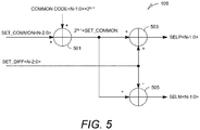
- FIG. 5 is a logic diagram of a threshold adjustment control circuit 109, according to example embodiments. This diagram is for purposes of illustration only as other ways to generate the selection words SELP and SELM for the DACs may be used.
- SET_COMMON and SET_DIFF are input values to the threshold adjustment control circuit 109. These values are set by a user of the circuit to change its behavior based on circuit characteristics (e.g., DAC resolution, V DD ) and desired performance of the adjustment.
- SET_COMMON represents a value input by the user based on the general common circuit deviation characteristics and/or DAC resolution, power supply voltage.
- SET DIFF represents a value input by the user for the desired voltage difference that the positive data signal is pulled up and the negative data signal is pulled down.
- the present embodiments disclose a full range of the DAC as being from 0V to V DD *((2 N - 1)/(2 N )) which is approximately V DD .
- the 2's complement binary value having N-1 bits SET_COMMON may be set between negative V DD /4 which is -V DD *((2 N-2 - 1)/(2 N )) to positive VDD/4 which is +V DD *((2 N-2 -1)/(2 N )).
- the SET_COMMON code is summed to COMMON_CODE at 501 to generate a calculated common code of COMMON_CODE (e.g., 2 N-1 ) + SET _COMMON.
- the calculated common code is added at 503 to a two's complement binary number having N-1 bits and representing the common mode deviation from the common code (i.e., SET_DIFF ⁇ N-2:0>).
- the sum of these values is the SELP ⁇ N-1:0> select word.
- the SET_DIFF ⁇ N-2:0> value is also subtracted from the calculated common code COMMON CODE (e.g., 2 N-1 ) + SET_COMMON at 505.
- This operation generates the SELM ⁇ N-1:0> select word.
- the SET_COMMON 0,
- the SET DIFF 0.
- FIG. 6 is a block diagram of an optical module system 600 incorporating the threshold adjustment circuit 105, according to example embodiments.
- the optical module block diagram is for purposes of illustrating one use of the threshold adjustment circuit 105. Other embodiments may use the circuit 105 for other uses.
- the optical module 600 may be used in an optical communication system where optical data is transmitted over optical fiber to the optical-to-electrical conversion circuit 101.
- the optical-to-electrical conversion circuit 101 converts the single-ended optical data signal to a differential electrical data signal that is input through the termination circuit 103 to the linear equalizer circuit 107.
- the threshold adjustment circuit 105 provides the pull up of the zero-crossing point of the positive data and the pull down of the zero-crossing point of the negative data.
- the resulting data signals are equalized and input to the clock and data recover circuit 601 to re-time the differential electrical data signals.
- the re-timed signals are input to a driver circuit 603 for transmission to a host 605 for interpretation and/or storage of the data.
- the host 605 may be a computer or some kind of controller.
- FIG. 7 is a flowchart of a method for threshold adjustment compensation of optical noise when generating electrical data signals from an optical data signal, according to example embodiments.
- the optical data signal is converted to first and second differential electrical data signals through the optical-to-electrical conversion circuit.
- first and second threshold adjust signals are generated based on circuit characteristics.
- a zero-crossing point of the first and second differential data signals is adjusted based on the respective first and second threshold adjust signals such that the zero-crossing point of the positive data signal is pulled up and the zero-crossing point of the negative data signal is pulled down.
- the first and second differential electrical data signals are equalized after the zero-crossing points of each signal has been adjusted in order to generate the electrical data signals.
- FIG. 8 is a block diagram of a threshold adjustment compensation apparatus, according to example embodiments.
- Block 801 of the apparatus comprises optical signal-to-electrical signal conversion means for converting an optical data signal to first and second differential electrical data signals.
- this means may include any optical signal-to-electrical signal conversion device such as a photo diode to generate electrical signals in response to the optical signals.
- the apparatus includes first and second threshold adjust signal generation means for generating first and second threshold adjust signals based on a default code and circuit characteristics.
- this means may include a circuit such as one illustrated in FIG. 5 .
- the apparatus includes zero-crossing point adjustment means for adjusting a zero-crossing point of the first and second differential data signals based on the respective first and second threshold adjust signals such that the zero-crossing point of positive data is pulled up and the zero-crossing point of negative data is pulled down.
- this means may include one or more DAC circuits.
- the apparatus includes equalizing means for equalizing the first and second differential data signals after the zero-crossing points of each signal has been adjusted to generate the electrical data signals.
- this means may include any circuit configured to equalize signals.
- a system for threshold adjustment compensation of optical noise when generating electrical data signals from an optical data signal includes converting means for converting the optical data signal to first and second differential electrical data signals.
- the system further includes generating means for generating first and second threshold adjust signals based on a default code and circuit characteristics.
- the system includes adjusting means for adjusting a zero-crossing point of the first and second differential data signals based on the respective first and second threshold adjust signals such that the zero-crossing point of positive data is pulled up and the zero-crossing point of negative data is pulled down.
- the system includes equalizing means for equalizing the first and second differential data signals after the zero-crossing points of each signal has been adjusted to generate the electrical data signals.
- the functions or algorithms described herein may be implemented in software in one embodiment.
- the software may consist of computer executable instructions stored on computer readable media or computer readable storage device such as one or more non-transitory memories or other type of hardware based storage devices, either local or networked.
- modules which may be software, hardware, firmware or any combination thereof. Multiple functions may be performed in one or more modules as desired, and the embodiments described are merely examples.
- the software may be executed on a digital signal processor, ASIC, microprocessor, or other type of processor operating on a computer system, such as a personal computer, server or other computer system, turning such computer system into a specifically programmed machine.
Landscapes
- Engineering & Computer Science (AREA)
- Physics & Mathematics (AREA)
- Electromagnetism (AREA)
- Computer Networks & Wireless Communication (AREA)
- Signal Processing (AREA)
- Theoretical Computer Science (AREA)
- Dc Digital Transmission (AREA)
Claims (20)
- Circuit de données optique comprenant :un circuit de conversion optique-électrique (101) configuré pour produire des premier et second signaux de données électriques différentiels, au niveau de premier et second nœuds électriques (P1, N1) respectifs, en réponse à un signal de données optique ;un premier circuit convertisseur numérique-analogique, CNA, (230) couplé au premier nœud électrique (P1) et configuré pour générer un premier signal d'ajustement ; etun second circuit CNA (231) couplé au second nœud électrique (N1) et configuré pour générer un second signal d'ajustement ;les premier (230) et second circuits CNA (231) étant configurés pour ajuster les premier et second signaux de données électriques différentiels de telle sorte qu'un point de passage à zéro d'un signal de données positives soit relevé en réponse au premier signal d'ajustement et qu'un point de passage à zéro d'un signal de données négatives soit abaissé en réponse au second signal d'ajustement.
- Circuit selon la revendication 1, dans lequel les premier et second circuits CNA (230, 231) comprennent des premier et second circuits CNA R-2R comprenant une pluralité de circuits de sélection (401-409) pour sélectionner un circuit diviseur de tension à résistance respectif en réponse à un premier ou second mot de commande de sélection respectif.
- Circuit selon l'une quelconque des revendications 1 à 2, comprenant en outre un circuit de commande d'ajustement de seuil (109) couplé aux premier et second circuits CNA (230, 231), le circuit de commande d'ajustement de seuil (109) étant configuré pour générer les premier et second mots de commande de sélection.
- Circuit selon l'une quelconque des revendications 1 à 3, dans lequel le circuit de commande d'ajustement de seuil (109) est configuré pour générer les premier et second mots de commande de sélection sur la base d'un code par défaut câblé et de caractéristiques du circuit.
- Circuit selon l'une quelconque des revendications 1 à 4, dans lequel le premier circuit CNA (230) est configuré pour ajuster le point de passage à zéro des données positives en réponse au premier mot de commande de sélection et le second circuit CNA (231) est configuré pour ajuster le point de passage à zéro des données négatives en réponse au second mot de commande de sélection.
- Circuit selon l'une quelconque des revendications 1 à 5, comprenant en outre un circuit de terminaison (103) couplé aux premier et second nœuds électriques (P1, N1).
- Circuit selon l'une quelconque des revendications 1 à 6, comprenant en outre :une première capacité (210) couplée entre le premier nœud électrique (P1) et le premier circuit CNA (230) ; etune seconde capacité (211) couplée entre le second nœud électrique (N1) et le second circuit CNA (231).
- Circuit selon l'une quelconque des revendications 1 à 7, dans lequel les premier et second circuits CNA (230, 21) sont respectivement couplés aux première et seconde capacités (210, 211) par le biais d'une première et d'une seconde résistance (220, 221) respectives.
- Circuit selon l'une quelconque des revendications 1 à 8, dans lequel les première et seconde résistances (220, 221) comprennent une valeur de résistance suffisamment grande pour éviter la déviation du signal CC des données positives et négatives aux entrées respectives (P2, N2) pour un circuit égaliseur linéaire (107).
- Système de communication optique comprenant :un circuit de conversion optique-électrique (101) configuré pour produire des premier et second signaux de données électriques différentiels, au niveau de premier et second nœuds électriques (P1, N1) respectifs, en réponse à un signal de données optique asymétrique ;un circuit de terminaison (103) couplé aux premier et second nœuds électriques (P1, N1) ;un premier circuit convertisseur numérique-analogique, CNA, (230) couplé au premier nœud électrique (P1), le premier circuit CNA (230) comprenant une première entrée binaire et une première sortie de tension ;un second circuit CNA (231) couplé au second nœud électrique (N1), le second circuit CNA (231) comprenant une seconde entrée binaire et une seconde sortie de tension ; etun circuit égaliseur linéaire (107) couplé au circuit de terminaison (103) et aux premier et second circuits CNA (230, 231) ; etles premier et second circuits CNA (230, 231) étant configurés pour ajuster les premier et second signaux de données électriques différentiels en fonction des première et seconde sorties de tension respectives de telle sorte qu'un point de passage à zéro d'un signal de données positives soit relevé et qu'un point de passage à zéro d'un signal de données négatives soit abaissé.
- Système selon la revendication 10, comprenant en outre un circuit de récupération d'horloge et de données (601) couplé à des sorties différentielles du circuit égaliseur linéaire, le circuit de récupération d'horloge et de données étant configuré pour resynchroniser les signaux de données électriques différentiels.
- Système selon l'une quelconque des revendications 10 à 11, comprenant en outre un circuit d'attaque (603) couplé au circuit de récupération d'horloge et de données, le circuit d'attaque (603) étant configuré pour transmettre les signaux de données électriques différentiels resynchronisés à un hôte.
- Système selon l'une quelconque des revendications 10 à 12, dans lequel le circuit de terminaison (103) comprend une première résistance (201) couplée entre le premier nœud électrique (P1) et un nœud d'alimentation électrique (VTERM) et une seconde résistance (202) couplée entre le second nœud électrique (N1) et le nœud d'alimentation électrique (VTERM).
- Système selon l'une quelconque des revendications 10 à 13, comprenant en outre un circuit de commande d'ajustement de seuil (109) couplé aux premier et second circuits CNA (230, 231) et configuré pour générer des mots de commande de sélection positive et négative respectivement au niveau des première et seconde entrées binaires.
- Procédé de compensation par ajustement de seuil de bruit optique lors de la génération de signaux de données électriques à partir d'un signal de données optique, le procédé comprenant :la conversion du signal de données optique en premier et second signaux de données électriques différentiels ;la génération des premier et second signaux d'ajustement de seuil sur la base d'un code par défaut et de caractéristiques de circuit ;l'ajustement d'un point de passage à zéro des premier et second signaux de données différentiels sur la base des premier et second signaux d'ajustement de seuil respectifs de telle sorte que le point de passage à zéro des données positives soit relevé et que le point de passage à zéro des données négatives soit abaissé ; etl'égalisation des premier et second signaux de données différentiels après que les points de passage à zéro de chaque signal ont été ajustés pour générer les signaux de données électriques.
- Procédé selon la revendication 15, comprenant en outre la resynchronisation des signaux de données électriques pour récupérer les données positives et négatives.
- Procédé selon l'une quelconque des revendications 15 à 16, selon lequel la génération des premier et second signaux d'ajustement de seuil comprend :la réception d'une valeur représentant les caractéristiques d'écart de circuit communes ;la réception d'une valeur de la différence de tension souhaitée ;l'addition de la valeur représentant les caractéristiques d'écart de circuit communes à un code de caractéristiques de circuit commun stocké et à la valeur de la différence de tension souhaitée pour générer un mot de commande de sélection positive ; etla soustraction de la valeur de la différence de tension souhaitée de la somme de la valeur représentant les caractéristiques d'écart de circuit communes et du code de caractéristiques de circuit commun stocké pour générer un mot de commande de sélection négative.
- Procédé selon l'une quelconque des revendications 15 à 17, comprenant en outre la génération du premier signal d'ajustement de seuil par un premier circuit convertisseur numérique-analogique, CNA, (230) avec le mot de commande de sélection positive.
- Procédé selon l'une quelconque des revendications 15 à 18, comprenant en outre la génération du second signal d'ajustement de seuil par un second circuit CNA (231) avec le mot de commande de sélection négative.
- Procédé selon l'une quelconque des revendications 15 à 19, selon lequel le mot de commande de sélection positive et le mot de commande de sélection négative sélectionnent un ou plusieurs circuits diviseurs de tension dans le premier ou le second circuit CNA (230, 231) pour générer le premier ou le second signal d'ajustement.
Applications Claiming Priority (2)
| Application Number | Priority Date | Filing Date | Title |
|---|---|---|---|
| US15/429,492 US10097266B2 (en) | 2017-02-10 | 2017-02-10 | Threshold adjustment compensation of asymmetrical optical noise |
| PCT/CN2018/075788 WO2018145643A1 (fr) | 2017-02-10 | 2018-02-08 | Compensation par ajustement de seuil de bruit optique asymétrique |
Publications (3)
| Publication Number | Publication Date |
|---|---|
| EP3574585A1 EP3574585A1 (fr) | 2019-12-04 |
| EP3574585A4 EP3574585A4 (fr) | 2020-01-08 |
| EP3574585B1 true EP3574585B1 (fr) | 2021-04-07 |
Family
ID=63104867
Family Applications (1)
| Application Number | Title | Priority Date | Filing Date |
|---|---|---|---|
| EP18751499.7A Active EP3574585B1 (fr) | 2017-02-10 | 2018-02-08 | Compensation par ajustement de seuil de bruit optique asymétrique |
Country Status (4)
| Country | Link |
|---|---|
| US (2) | US10097266B2 (fr) |
| EP (1) | EP3574585B1 (fr) |
| CN (2) | CN112187260B (fr) |
| WO (1) | WO2018145643A1 (fr) |
Families Citing this family (5)
| Publication number | Priority date | Publication date | Assignee | Title |
|---|---|---|---|---|
| US10097266B2 (en) | 2017-02-10 | 2018-10-09 | Futurewei Technologies, Inc. | Threshold adjustment compensation of asymmetrical optical noise |
| US10656336B1 (en) | 2018-11-08 | 2020-05-19 | Luminous Computing, Inc. | Method for phase-based photonic computing |
| US11016315B2 (en) | 2019-07-11 | 2021-05-25 | Luminous Computing, Inc. | Photonic bandgap phase modulator, optical filter bank, photonic computing system, and methods of use |
| US12045080B1 (en) | 2020-02-07 | 2024-07-23 | Luminous Computing, Inc. | Optical computing system and method of use |
| US11211941B2 (en) * | 2020-03-14 | 2021-12-28 | Luminous Computing, Inc. | Digital-to-analog converter system and method of operation |
Family Cites Families (20)
| Publication number | Priority date | Publication date | Assignee | Title |
|---|---|---|---|---|
| KR19990075000A (ko) * | 1998-03-17 | 1999-10-05 | 윤종용 | 클램프 레벨 및 입력 오프셋을 조절하는 광전 변환 회로 |
| US6172630B1 (en) * | 1998-08-18 | 2001-01-09 | Tektronix, Inc. | Extended common mode input range for a delta-sigma converter |
| US7453388B1 (en) * | 2002-07-17 | 2008-11-18 | Silicon Laboratories Inc. | Slice voltage compensation |
| US7184478B2 (en) * | 2003-06-19 | 2007-02-27 | Applied Micro Circuits Corporation | High speed circuits for electronic dispersion compensation |
| GB2405295B (en) * | 2003-08-19 | 2006-10-25 | Agilent Technologies Inc | Variable decision threshold apparatus |
| US7522848B2 (en) * | 2004-09-30 | 2009-04-21 | Emcore Corporation | Receiver with dynamically adjustable decision threshold voltage based on input power |
| JP2006121387A (ja) | 2004-10-21 | 2006-05-11 | Nec Corp | 識別再生方法および識別再生装置 |
| US7406269B2 (en) * | 2006-03-10 | 2008-07-29 | Discovery Semiconductors, Inc. | Feedback-controlled coherent optical receiver with electrical compensation/equalization |
| US7543388B2 (en) * | 2006-05-02 | 2009-06-09 | Northern Building Solutions, Inc. | Reveal tool |
| JP4782667B2 (ja) | 2006-12-26 | 2011-09-28 | 三菱電機株式会社 | 光受信器 |
| US8917783B2 (en) | 2008-12-03 | 2014-12-23 | Rambus Inc. | Resonance mitigation for high-speed signaling |
| CN101949684B (zh) * | 2010-09-06 | 2012-11-28 | 西安交通大学 | 一种基于移动比较的双频激光干涉仪信号高倍频细分系统 |
| WO2013042175A1 (fr) | 2011-09-22 | 2013-03-28 | Nec Corporation | Dispositif de sortie optique et procédé de commande d'un émetteur optique |
| WO2013174376A2 (fr) * | 2012-05-22 | 2013-11-28 | Silicon Line Gmbh | Ensemble circuit et procédé de réception de signaux optiques numériques |
| CN203719792U (zh) * | 2014-01-03 | 2014-07-16 | 上海光维通信技术股份有限公司 | 分布式光纤测温装置 |
| US9335370B2 (en) * | 2014-01-16 | 2016-05-10 | Globalfoundries Inc. | On-chip test for integrated AC coupling capacitors |
| US9590730B2 (en) * | 2014-10-01 | 2017-03-07 | Futurewei Technologies, Inc. | Optical transmitter with optical receiver-specific dispersion pre-compensation |
| CN104751756B (zh) * | 2015-04-23 | 2017-12-12 | 京东方科技集团股份有限公司 | 显示面板的光学调节装置、方法和显示装置 |
| US10097266B2 (en) | 2017-02-10 | 2018-10-09 | Futurewei Technologies, Inc. | Threshold adjustment compensation of asymmetrical optical noise |
| CN107204805B (zh) * | 2017-04-25 | 2019-08-02 | 上海交通大学 | 用于多模多电平调制短距光通信系统幅度域及时间域均衡方法 |
-
2017
- 2017-02-10 US US15/429,492 patent/US10097266B2/en active Active
-
2018
- 2018-02-08 CN CN202010897429.0A patent/CN112187260B/zh active Active
- 2018-02-08 WO PCT/CN2018/075788 patent/WO2018145643A1/fr not_active Ceased
- 2018-02-08 CN CN201880011308.2A patent/CN110301096B/zh active Active
- 2018-02-08 EP EP18751499.7A patent/EP3574585B1/fr active Active
- 2018-10-08 US US16/154,448 patent/US10454580B2/en active Active
Non-Patent Citations (1)
| Title |
|---|
| None * |
Also Published As
| Publication number | Publication date |
|---|---|
| US20190052363A1 (en) | 2019-02-14 |
| US10454580B2 (en) | 2019-10-22 |
| EP3574585A1 (fr) | 2019-12-04 |
| CN110301096B (zh) | 2020-09-11 |
| WO2018145643A1 (fr) | 2018-08-16 |
| US10097266B2 (en) | 2018-10-09 |
| EP3574585A4 (fr) | 2020-01-08 |
| CN112187260A (zh) | 2021-01-05 |
| CN110301096A (zh) | 2019-10-01 |
| CN112187260B (zh) | 2024-06-11 |
| US20180234183A1 (en) | 2018-08-16 |
Similar Documents
| Publication | Publication Date | Title |
|---|---|---|
| EP3574585B1 (fr) | Compensation par ajustement de seuil de bruit optique asymétrique | |
| US7496161B2 (en) | Adaptive equalization system for a signal receiver | |
| KR102279089B1 (ko) | 전압-모드 드라이버에 대한 임피던스 및 스윙 제어 | |
| US10164802B1 (en) | Full bridge decision feedback equalizer | |
| Song et al. | A 6-Gbit/s hybrid voltage-mode transmitter with current-mode equalization in 90-nm CMOS | |
| US9735879B2 (en) | Near-threshold optical transmitter pre-distortion | |
| US9853642B1 (en) | Data-dependent current compensation in a voltage-mode driver | |
| US6140857A (en) | Method and apparatus for reducing baseline wander | |
| US10027516B2 (en) | Receiver with offset calibration | |
| CN107645342B (zh) | 信号丢失检测设备和方法 | |
| US10797658B1 (en) | Low power optical link | |
| US10341147B1 (en) | High performance equalizer achieving low deterministic jitter across PVT for various channel lengths and data rates | |
| US12107707B2 (en) | Method and apparatus for low latency charge coupled decision feedback equalization | |
| US20200358639A1 (en) | Reception circuit, receiver, and reception control method | |
| CN116192579A (zh) | 包括偏移补偿电路的接收器 | |
| JP2015517774A (ja) | デジタル光信号を受信するための回路装置及び方法 | |
| US7656248B2 (en) | Equalizer and related signal equalizing method | |
| US10312920B2 (en) | Baseline wander compensation | |
| CN115086117A (zh) | 一种判决反馈方法及判决反馈均衡器 | |
| TWI663840B (zh) | 自適應接收等化器調節電路及利用其之通信裝置 | |
| JP2017123606A (ja) | 送信装置 | |
| US12526177B2 (en) | Equalizer including an amplifying adder and receiver comprising the equalizer | |
| US20210091981A1 (en) | Signal output circuit, transmission circuit and integrated circuit | |
| KR20230080278A (ko) | 수신기 |
Legal Events
| Date | Code | Title | Description |
|---|---|---|---|
| STAA | Information on the status of an ep patent application or granted ep patent |
Free format text: STATUS: THE INTERNATIONAL PUBLICATION HAS BEEN MADE |
|
| PUAI | Public reference made under article 153(3) epc to a published international application that has entered the european phase |
Free format text: ORIGINAL CODE: 0009012 |
|
| STAA | Information on the status of an ep patent application or granted ep patent |
Free format text: STATUS: REQUEST FOR EXAMINATION WAS MADE |
|
| 17P | Request for examination filed |
Effective date: 20190826 |
|
| AK | Designated contracting states |
Kind code of ref document: A1 Designated state(s): AL AT BE BG CH CY CZ DE DK EE ES FI FR GB GR HR HU IE IS IT LI LT LU LV MC MK MT NL NO PL PT RO RS SE SI SK SM TR |
|
| AX | Request for extension of the european patent |
Extension state: BA ME |
|
| RIN1 | Information on inventor provided before grant (corrected) |
Inventor name: LEE, HUNG-YI Inventor name: CAO, YUMING Inventor name: GU, LIANG Inventor name: LIU, MIAO |
|
| A4 | Supplementary search report drawn up and despatched |
Effective date: 20191205 |
|
| RIC1 | Information provided on ipc code assigned before grant |
Ipc: H04B 10/69 20130101ALI20191130BHEP Ipc: H04B 3/04 20060101ALI20191130BHEP Ipc: H04B 1/16 20060101AFI20191130BHEP |
|
| DAV | Request for validation of the european patent (deleted) | ||
| DAX | Request for extension of the european patent (deleted) | ||
| GRAJ | Information related to disapproval of communication of intention to grant by the applicant or resumption of examination proceedings by the epo deleted |
Free format text: ORIGINAL CODE: EPIDOSDIGR1 |
|
| STAA | Information on the status of an ep patent application or granted ep patent |
Free format text: STATUS: GRANT OF PATENT IS INTENDED |
|
| GRAP | Despatch of communication of intention to grant a patent |
Free format text: ORIGINAL CODE: EPIDOSNIGR1 |
|
| INTG | Intention to grant announced |
Effective date: 20200925 |
|
| GRAS | Grant fee paid |
Free format text: ORIGINAL CODE: EPIDOSNIGR3 |
|
| GRAA | (expected) grant |
Free format text: ORIGINAL CODE: 0009210 |
|
| STAA | Information on the status of an ep patent application or granted ep patent |
Free format text: STATUS: THE PATENT HAS BEEN GRANTED |
|
| AK | Designated contracting states |
Kind code of ref document: B1 Designated state(s): AL AT BE BG CH CY CZ DE DK EE ES FI FR GB GR HR HU IE IS IT LI LT LU LV MC MK MT NL NO PL PT RO RS SE SI SK SM TR |
|
| REG | Reference to a national code |
Ref country code: GB Ref legal event code: FG4D |
|
| REG | Reference to a national code |
Ref country code: AT Ref legal event code: REF Ref document number: 1381019 Country of ref document: AT Kind code of ref document: T Effective date: 20210415 Ref country code: CH Ref legal event code: EP |
|
| REG | Reference to a national code |
Ref country code: DE Ref legal event code: R096 Ref document number: 602018015296 Country of ref document: DE |
|
| REG | Reference to a national code |
Ref country code: IE Ref legal event code: FG4D |
|
| REG | Reference to a national code |
Ref country code: LT Ref legal event code: MG9D |
|
| REG | Reference to a national code |
Ref country code: NL Ref legal event code: MP Effective date: 20210407 Ref country code: AT Ref legal event code: MK05 Ref document number: 1381019 Country of ref document: AT Kind code of ref document: T Effective date: 20210407 |
|
| PG25 | Lapsed in a contracting state [announced via postgrant information from national office to epo] |
Ref country code: NL Free format text: LAPSE BECAUSE OF FAILURE TO SUBMIT A TRANSLATION OF THE DESCRIPTION OR TO PAY THE FEE WITHIN THE PRESCRIBED TIME-LIMIT Effective date: 20210407 Ref country code: AT Free format text: LAPSE BECAUSE OF FAILURE TO SUBMIT A TRANSLATION OF THE DESCRIPTION OR TO PAY THE FEE WITHIN THE PRESCRIBED TIME-LIMIT Effective date: 20210407 Ref country code: BG Free format text: LAPSE BECAUSE OF FAILURE TO SUBMIT A TRANSLATION OF THE DESCRIPTION OR TO PAY THE FEE WITHIN THE PRESCRIBED TIME-LIMIT Effective date: 20210707 Ref country code: FI Free format text: LAPSE BECAUSE OF FAILURE TO SUBMIT A TRANSLATION OF THE DESCRIPTION OR TO PAY THE FEE WITHIN THE PRESCRIBED TIME-LIMIT Effective date: 20210407 Ref country code: LT Free format text: LAPSE BECAUSE OF FAILURE TO SUBMIT A TRANSLATION OF THE DESCRIPTION OR TO PAY THE FEE WITHIN THE PRESCRIBED TIME-LIMIT Effective date: 20210407 Ref country code: HR Free format text: LAPSE BECAUSE OF FAILURE TO SUBMIT A TRANSLATION OF THE DESCRIPTION OR TO PAY THE FEE WITHIN THE PRESCRIBED TIME-LIMIT Effective date: 20210407 |
|
| PG25 | Lapsed in a contracting state [announced via postgrant information from national office to epo] |
Ref country code: NO Free format text: LAPSE BECAUSE OF FAILURE TO SUBMIT A TRANSLATION OF THE DESCRIPTION OR TO PAY THE FEE WITHIN THE PRESCRIBED TIME-LIMIT Effective date: 20210707 Ref country code: LV Free format text: LAPSE BECAUSE OF FAILURE TO SUBMIT A TRANSLATION OF THE DESCRIPTION OR TO PAY THE FEE WITHIN THE PRESCRIBED TIME-LIMIT Effective date: 20210407 Ref country code: PL Free format text: LAPSE BECAUSE OF FAILURE TO SUBMIT A TRANSLATION OF THE DESCRIPTION OR TO PAY THE FEE WITHIN THE PRESCRIBED TIME-LIMIT Effective date: 20210407 Ref country code: RS Free format text: LAPSE BECAUSE OF FAILURE TO SUBMIT A TRANSLATION OF THE DESCRIPTION OR TO PAY THE FEE WITHIN THE PRESCRIBED TIME-LIMIT Effective date: 20210407 Ref country code: PT Free format text: LAPSE BECAUSE OF FAILURE TO SUBMIT A TRANSLATION OF THE DESCRIPTION OR TO PAY THE FEE WITHIN THE PRESCRIBED TIME-LIMIT Effective date: 20210809 Ref country code: SE Free format text: LAPSE BECAUSE OF FAILURE TO SUBMIT A TRANSLATION OF THE DESCRIPTION OR TO PAY THE FEE WITHIN THE PRESCRIBED TIME-LIMIT Effective date: 20210407 Ref country code: GR Free format text: LAPSE BECAUSE OF FAILURE TO SUBMIT A TRANSLATION OF THE DESCRIPTION OR TO PAY THE FEE WITHIN THE PRESCRIBED TIME-LIMIT Effective date: 20210708 Ref country code: IS Free format text: LAPSE BECAUSE OF FAILURE TO SUBMIT A TRANSLATION OF THE DESCRIPTION OR TO PAY THE FEE WITHIN THE PRESCRIBED TIME-LIMIT Effective date: 20210807 |
|
| REG | Reference to a national code |
Ref country code: DE Ref legal event code: R097 Ref document number: 602018015296 Country of ref document: DE |
|
| PG25 | Lapsed in a contracting state [announced via postgrant information from national office to epo] |
Ref country code: RO Free format text: LAPSE BECAUSE OF FAILURE TO SUBMIT A TRANSLATION OF THE DESCRIPTION OR TO PAY THE FEE WITHIN THE PRESCRIBED TIME-LIMIT Effective date: 20210407 Ref country code: SM Free format text: LAPSE BECAUSE OF FAILURE TO SUBMIT A TRANSLATION OF THE DESCRIPTION OR TO PAY THE FEE WITHIN THE PRESCRIBED TIME-LIMIT Effective date: 20210407 Ref country code: DK Free format text: LAPSE BECAUSE OF FAILURE TO SUBMIT A TRANSLATION OF THE DESCRIPTION OR TO PAY THE FEE WITHIN THE PRESCRIBED TIME-LIMIT Effective date: 20210407 Ref country code: CZ Free format text: LAPSE BECAUSE OF FAILURE TO SUBMIT A TRANSLATION OF THE DESCRIPTION OR TO PAY THE FEE WITHIN THE PRESCRIBED TIME-LIMIT Effective date: 20210407 Ref country code: SK Free format text: LAPSE BECAUSE OF FAILURE TO SUBMIT A TRANSLATION OF THE DESCRIPTION OR TO PAY THE FEE WITHIN THE PRESCRIBED TIME-LIMIT Effective date: 20210407 Ref country code: ES Free format text: LAPSE BECAUSE OF FAILURE TO SUBMIT A TRANSLATION OF THE DESCRIPTION OR TO PAY THE FEE WITHIN THE PRESCRIBED TIME-LIMIT Effective date: 20210407 Ref country code: EE Free format text: LAPSE BECAUSE OF FAILURE TO SUBMIT A TRANSLATION OF THE DESCRIPTION OR TO PAY THE FEE WITHIN THE PRESCRIBED TIME-LIMIT Effective date: 20210407 |
|
| PLBE | No opposition filed within time limit |
Free format text: ORIGINAL CODE: 0009261 |
|
| STAA | Information on the status of an ep patent application or granted ep patent |
Free format text: STATUS: NO OPPOSITION FILED WITHIN TIME LIMIT |
|
| 26N | No opposition filed |
Effective date: 20220110 |
|
| PG25 | Lapsed in a contracting state [announced via postgrant information from national office to epo] |
Ref country code: IS Free format text: LAPSE BECAUSE OF FAILURE TO SUBMIT A TRANSLATION OF THE DESCRIPTION OR TO PAY THE FEE WITHIN THE PRESCRIBED TIME-LIMIT Effective date: 20210807 Ref country code: AL Free format text: LAPSE BECAUSE OF FAILURE TO SUBMIT A TRANSLATION OF THE DESCRIPTION OR TO PAY THE FEE WITHIN THE PRESCRIBED TIME-LIMIT Effective date: 20210407 |
|
| PG25 | Lapsed in a contracting state [announced via postgrant information from national office to epo] |
Ref country code: IT Free format text: LAPSE BECAUSE OF FAILURE TO SUBMIT A TRANSLATION OF THE DESCRIPTION OR TO PAY THE FEE WITHIN THE PRESCRIBED TIME-LIMIT Effective date: 20210407 |
|
| PG25 | Lapsed in a contracting state [announced via postgrant information from national office to epo] |
Ref country code: MC Free format text: LAPSE BECAUSE OF FAILURE TO SUBMIT A TRANSLATION OF THE DESCRIPTION OR TO PAY THE FEE WITHIN THE PRESCRIBED TIME-LIMIT Effective date: 20210407 |
|
| REG | Reference to a national code |
Ref country code: CH Ref legal event code: PL |
|
| REG | Reference to a national code |
Ref country code: BE Ref legal event code: MM Effective date: 20220228 |
|
| PG25 | Lapsed in a contracting state [announced via postgrant information from national office to epo] |
Ref country code: LU Free format text: LAPSE BECAUSE OF NON-PAYMENT OF DUE FEES Effective date: 20220208 |
|
| PG25 | Lapsed in a contracting state [announced via postgrant information from national office to epo] |
Ref country code: FR Free format text: LAPSE BECAUSE OF NON-PAYMENT OF DUE FEES Effective date: 20220228 |
|
| PG25 | Lapsed in a contracting state [announced via postgrant information from national office to epo] |
Ref country code: LI Free format text: LAPSE BECAUSE OF NON-PAYMENT OF DUE FEES Effective date: 20220228 Ref country code: IE Free format text: LAPSE BECAUSE OF NON-PAYMENT OF DUE FEES Effective date: 20220208 Ref country code: CH Free format text: LAPSE BECAUSE OF NON-PAYMENT OF DUE FEES Effective date: 20220228 |
|
| PG25 | Lapsed in a contracting state [announced via postgrant information from national office to epo] |
Ref country code: BE Free format text: LAPSE BECAUSE OF NON-PAYMENT OF DUE FEES Effective date: 20220228 |
|
| P01 | Opt-out of the competence of the unified patent court (upc) registered |
Effective date: 20230524 |
|
| PG25 | Lapsed in a contracting state [announced via postgrant information from national office to epo] |
Ref country code: MK Free format text: LAPSE BECAUSE OF FAILURE TO SUBMIT A TRANSLATION OF THE DESCRIPTION OR TO PAY THE FEE WITHIN THE PRESCRIBED TIME-LIMIT Effective date: 20210407 Ref country code: CY Free format text: LAPSE BECAUSE OF FAILURE TO SUBMIT A TRANSLATION OF THE DESCRIPTION OR TO PAY THE FEE WITHIN THE PRESCRIBED TIME-LIMIT Effective date: 20210407 |
|
| PG25 | Lapsed in a contracting state [announced via postgrant information from national office to epo] |
Ref country code: HU Free format text: LAPSE BECAUSE OF FAILURE TO SUBMIT A TRANSLATION OF THE DESCRIPTION OR TO PAY THE FEE WITHIN THE PRESCRIBED TIME-LIMIT; INVALID AB INITIO Effective date: 20180208 |
|
| PG25 | Lapsed in a contracting state [announced via postgrant information from national office to epo] |
Ref country code: TR Free format text: LAPSE BECAUSE OF FAILURE TO SUBMIT A TRANSLATION OF THE DESCRIPTION OR TO PAY THE FEE WITHIN THE PRESCRIBED TIME-LIMIT Effective date: 20210407 |
|
| PG25 | Lapsed in a contracting state [announced via postgrant information from national office to epo] |
Ref country code: MT Free format text: LAPSE BECAUSE OF FAILURE TO SUBMIT A TRANSLATION OF THE DESCRIPTION OR TO PAY THE FEE WITHIN THE PRESCRIBED TIME-LIMIT Effective date: 20210407 |
|
| PGFP | Annual fee paid to national office [announced via postgrant information from national office to epo] |
Ref country code: GB Payment date: 20260106 Year of fee payment: 9 |
|
| PGFP | Annual fee paid to national office [announced via postgrant information from national office to epo] |
Ref country code: DE Payment date: 20251230 Year of fee payment: 9 |