EP3577594B1 - Dispositif et utilisation du dispositif de génération d'un signal variable dépendant du temps dans un capteur capacitif de superficie - Google Patents
Dispositif et utilisation du dispositif de génération d'un signal variable dépendant du temps dans un capteur capacitif de superficie Download PDFInfo
- Publication number
- EP3577594B1 EP3577594B1 EP18711812.0A EP18711812A EP3577594B1 EP 3577594 B1 EP3577594 B1 EP 3577594B1 EP 18711812 A EP18711812 A EP 18711812A EP 3577594 B1 EP3577594 B1 EP 3577594B1
- Authority
- EP
- European Patent Office
- Prior art keywords
- electrically conductive
- conductive structure
- surface sensor
- capacitive
- individual elements
- Prior art date
- Legal status (The legal status is an assumption and is not a legal conclusion. Google has not performed a legal analysis and makes no representation as to the accuracy of the status listed.)
- Active
Links
Images


Classifications
-
- G—PHYSICS
- G06—COMPUTING OR CALCULATING; COUNTING
- G06K—GRAPHICAL DATA READING; PRESENTATION OF DATA; RECORD CARRIERS; HANDLING RECORD CARRIERS
- G06K7/00—Methods or arrangements for sensing record carriers, e.g. for reading patterns
- G06K7/08—Methods or arrangements for sensing record carriers, e.g. for reading patterns by means detecting the change of an electrostatic or magnetic field, e.g. by detecting change of capacitance between electrodes
-
- G—PHYSICS
- G06—COMPUTING OR CALCULATING; COUNTING
- G06K—GRAPHICAL DATA READING; PRESENTATION OF DATA; RECORD CARRIERS; HANDLING RECORD CARRIERS
- G06K19/00—Record carriers for use with machines and with at least a part designed to carry digital markings
- G06K19/06—Record carriers for use with machines and with at least a part designed to carry digital markings characterised by the kind of the digital marking, e.g. shape, nature, code
- G06K19/067—Record carriers with conductive marks, printed circuits or semiconductor circuit elements, e.g. credit or identity cards also with resonating or responding marks without active components
-
- G—PHYSICS
- G06—COMPUTING OR CALCULATING; COUNTING
- G06K—GRAPHICAL DATA READING; PRESENTATION OF DATA; RECORD CARRIERS; HANDLING RECORD CARRIERS
- G06K19/00—Record carriers for use with machines and with at least a part designed to carry digital markings
- G06K19/06—Record carriers for use with machines and with at least a part designed to carry digital markings characterised by the kind of the digital marking, e.g. shape, nature, code
- G06K19/067—Record carriers with conductive marks, printed circuits or semiconductor circuit elements, e.g. credit or identity cards also with resonating or responding marks without active components
- G06K19/07—Record carriers with conductive marks, printed circuits or semiconductor circuit elements, e.g. credit or identity cards also with resonating or responding marks without active components with integrated circuit chips
- G06K19/077—Constructional details, e.g. mounting of circuits in the carrier
- G06K19/07749—Constructional details, e.g. mounting of circuits in the carrier the record carrier being capable of non-contact communication, e.g. constructional details of the antenna of a non-contact smart card
- G06K19/07773—Antenna details
- G06K19/07788—Antenna details the antenna being of the capacitive type
Definitions
- the invention relates to a system and a method for generating a time-dependent signal on a capacitive area sensor.
- optical codes are known in the form of classic bar codes (bar codes) or also 2D bar codes, for example data matrix or QR codes.
- OCR methods optical character recognition
- text recognition or optical character recognition are also frequently used for identification.
- OCR methods optical character recognition
- RFID tags are electronic circuits that are read using radio waves. These tags are much more copy-proof and counterfeit-proof compared to optical codes. However, for many mass applications, RFID tags are too expensive, particularly because large-scale applications are often required. In addition, RFID tags are not suitable for end customer applications because special reading devices are required. In the area of documents, the thickness of the RFID chip is also a problem, especially when large quantities of documents have to be marked and stored.
- capacitive data carriers have been developed in recent years, which combine the advantages of low costs and improved protection against counterfeiting.
- Capacitive data carriers in various forms are known from the prior art, as well as methods for their production and methods and systems for identifying the data carriers, including by means of touch screens, which are used, for example, in current smartphones and tablets. These capacitive data carriers are copy-proof, more cost-effective as optical codes and can be read by practically anyone using a mobile device such as a smartphone or tablet.
- capacitive data carriers which include an electrically conductive structure that are limited to a special arrangement of the elements of the conductive structure or must be structured according to certain rules in order to be recognized by a reader, for example a capacitive surface sensor, and /or to be read.
- the electrically conductive structures of the data carrier are fixed and cannot be subsequently changed or adjusted.
- these electrically conductive structures can usually trigger a specific signal on the reading device or area sensor, since the electrically conductive structure cannot be changed in terms of its spatial shape and is therefore always recognized as the same structure by the reading device.
- WO 2011/154524 A1 discloses a capacitive information carrier system for capturing information.
- the invention describes a system comprising a capacitive information carrier, in which an electrically conductive layer is arranged on an electrically non-conductive substrate, and an area sensor, the information carrier being in contact with the area sensor.
- the electrically conductive layer includes a touch structure that includes a touch point, a coupling surface and a conductor track.
- Such a structure can be evaluated with a data processing system connected to the area sensor and processed by software.
- the resulting touch inputs on the area sensor generate a static image of several touch points, which can be evaluated by the data processing system. Subsequent changes to the data carrier are not intended.
- WO 2014/064288 A1 or. US 2015/0286294 A1 describes a modular play figure for identification by touch screens, which comprises at least two modules, the second module being an identification means comprising at least one electrically conductive layer.
- This invention enables the exchange of the means of identification. In this case, too, a static image of touch points is evaluated.
- a cube is proposed, for example, on which an electrically conductive structure is applied, which is characterized by data points connected by conductor tracks.
- a touch input is recorded at the point of the data points.
- d sizes are preferred from 6 - 10 mm is required, as these imitate fingertips particularly well.
- the number of possible encodings is limited by the design constraint.
- the status of the identifier itself cannot easily be changed. This embodiment is limited to essentially three-dimensional objects and is not suitable for documents.
- the DE 1690334 A1 and the UK 2612653 disclose an electrical circuit board.
- a capacitive data carrier that can be detected using area sensors that are integrated into modern smartphones or tablets, for example, and that has the advantages already mentioned above compared to optical and radio-based systems (copy security, manipulation security, low costs). and can be changed or described later or to which a new status can be assigned later.
- the object of the present invention to provide a system and a method with which various signals can be generated on one reading device without affecting another to use data carriers with a different electrically conductive structure.
- the object of the invention is in particular to design a capacitive data carrier and the electrically conductive structure on the data carrier as part of a system in such a way that additional information is subsequently applied to the data carrier or that the data carrier can be subsequently provided with new status information that can be read using a surface sensor.
- the first electrically conductive structure is preferably also referred to as the electrically conductive basic structure and the second electrically conductive structure as the resultant electrically conductive structure.
- Both structures together are preferably referred to as "electrically conductive structures" within the meaning of the invention, this term preferably forming the generic term for the first and the second electrically conductive structure and thus preferably either both structures or one of the two structures can be meant.
- the two electrically conductive structures are not present on the device at the same time, but that the device initially, for example at a first point in time, comprises a first electrically conductive structure. The first conductive structure is then changed, the second electrically conductive structure being obtained as a result of the change in the first conductive structure. This is available, for example, at a later point in time on the device of the proposed system.
- the property that the first electrically conductive structure and the second electrically conductive structure are preferably not present on the device at the same time, but preferably one after the other, is preferably used in the context of the invention with the formulation that "the device has a first electrically conductive structure and a second electrically conductive structure includes".
- the dynamic input takes place by means of an input means on the device.
- the dynamic input preferably represents a movement, ie a dynamic process, of an input means on an electrically conductive structure, the electrically conductive structure being arranged on a device.
- the dynamic input preferably represents a relative movement between the device and an input means, in particular between an electrically conductive structure of the device and the input means.
- the input means can be a human finger, ie the finger of a human user of the device, or a stylus for use in connection with smartphones or the like, as are known from the prior art.
- a dynamic input takes place in the sense that an input means on the device or the electrically conductive structure of the device is moved , preferably relative to each other. It is very particularly preferred that the time-variable signal is generated by the dynamic input, that is to say in particular by the relative movement between the device and the input means.
- the dynamic input is modulated.
- the deviation is preferably caused by the form and/or shape of the electrically conductive structure, which is preferably set up to modulate the dynamic input.
- This process is preferably referred to as "modulation of a dynamic input” within the meaning of the invention.
- the signal is generated in the capacitive surface sensor, the signal preferably being defined and/or determined by the device and in particular by the electrically conductive structure on the device on the capacitive surface sensor.
- the changeable, time-dependent signal on the capacitive area sensor is defined by the first electrically conductive structure and/or the second electrically conductive structure.
- the area sensor can, for example, be part of a touch screen, as is used, for example, in newer mobile phones from 2007 or in tablet PCs.
- the area sensor is, for example, a component of a permanently installed data processing system, for example an information system at a touristically interesting location.
- the area sensor is part of a special reading device, which can be matched to the device, for example.
- the surface sensor is preferably set up to detect electrical signals that arise, for example, when an electrically conductive structure is in active contact with a surface sensor and a user makes a dynamic input using an input means on the electrically conductive structure, which is preferably on the device is arranged, makes.
- the first electrically conductive structure or the second electrically conductive structure is at least partially in operative contact with the capacitive area sensor.
- This dynamic input can, for example, take the form of a movement by the user on the device, as a result of which the electrically conductive structure is touched in whole or in part. It is particularly preferred within the meaning of the invention to designate a relative movement between an input means and the device as dynamic input, with a body part of a user or a pen specially provided for this purpose being able to be used as input means, for example.
- the movement represents, for example, a gesture, for example a swiping gesture.
- a stylus is used to alter a first electrically conductive pattern on a device to form a second electrically conductive pattern.
- the device on which there is a first electrically conductive structure to be changed is a device which is preferably characterized in that the first electrically conductive structure is set up to set a first signal on the capacitive area sensor, and the second electrically conductive structure is set up to set a second signal on the capacitive area sensor, wherein the second electrically conductive structure can be generated by changing the first electrically conductive structure.
- the first and the second electrically conductive structure are preferably present on the device one after the other and not simultaneously.
- the stylus is not the input stylus, which can be used, for example, as input means.
- the pin is preferably a pin with which, for example, electrically conductive material can be applied to the device. This can preferably be done by painting, drawing and/or writing on the device with the pen, the color and/or ink that is transferred to the device as a result of this process being, for example, electrically conductive ink and/or color.
- the electrically conductive ink and/or paint that is preferably contained in the pen can contain electrically conductive particles, as a result of which an electrical conductivity of the ink and/or paint is advantageously achieved.
- the pin is set up to remove part of the first electrically conductive structure from the device. This can happen, for example, in that the pen comprises means for erasing electrically conductive material, the term “erasing” in the sense of the invention preferably being understood as a removal or “erasing away”. It can also be preferred within the meaning of the invention that the pen has a function similar to an “ink killer” with which the electrically conductive structure present on the device can be removed or made invisible.
- the term “invisible” means that "invisible" areas of an electrically conductive structure are not recognizable, in particular for a capacitive area sensor, for example by reducing the electrical conductivity of the structure in such a way or by partially removing the electrically conductive structure so that the dynamic input is no longer modulated or modulated in a different way with an input means and is transmitted to the area sensor.
- the electrically conductive structure on the device of the proposed system comprises individual elements and that the dynamic input touches different individual elements at different points in time t i , for example by the dynamic input being swiped or linear movement of the input means is carried out, with which the user sweeps across the device, that is to say in particular the electrically conductive structure.
- This movement can preferably be referred to as a gesture.
- Points in time that relate to the dynamic input by an input means are preferably denoted by t i , ie t 1 , t 2 , t 3 , etc. in the following.
- the device of the proposed system can be constituted by a card, for example.
- the card can consist of an electrically non-conductive substrate material such as plastic, cardboard and/or paper and have the electrically conductive structure. It is preferred within the meaning of the invention that the first electrically conductive structure and/or the second electrically conductive structure is present on an electrically non-conductive substrate.
- the device preferably does not consist of objects provided in the form of foils, which comprise metal over their entire surface or are formed from metal, such as aluminum foil, for example.
- the card can have the shape and dimensions of a money card or another chip card, for example.
- the electrically conductive structure can preferably also be arranged on packaging, the packaging being present, for example, in a collapsed form (folded cardboard box) or in a 3D form (packaging filled with a product).
- the card can also be in the form of a sticker, sticker or label and can be applied alone or on a document or object. It is preferred within the meaning of the invention that the wording "electrically conductive structure" is used as a generic term for the electrically conductive basic structure and the second electrically conductive structure, in particular when the general shape and design of the electrically conductive structure is described, which is used both for the Basic structure as well as for the second electrically conductive structure applies.
- the electrically conductive basic structure is preferably also referred to as basic structure or first electrically conductive structure.
- the second electrically conductive structure is preferably also referred to as the resulting electrically conductive structure. It is generated by a subsequent modification of the electrically conductive basic structure.
- the device of the proposed system has a first electrically conductive structure that can be modified and/or processed, whereby a second electrically conductive structure is preferably obtained, which preferably differs from the first electrically conductive structure .
- a second electrically conductive structure is preferably obtained, which preferably differs from the first electrically conductive structure .
- the change in the first electrically conductive structure can be brought about with a pin.
- the pen is preferably set up to apply electrically conductive material to the device and/or to remove part of the first electrically conductive structure from the device, this removal preferably being carried out selectively, ie in particular not at random.
- the change in the first electrically conductive structure can preferably be brought about by a partial selective removal.
- this preferably means that the device of the proposed system and/or the electrically conductive structure on the device can be individually identified in the sense that two different devices can be distinguished from one another.
- the electrically conductive material is electrically conductive ink.
- two devices that have essentially the same first electrically conductive structures can be changed with a pen in such a way that the two devices, when the devices are brought into operative contact with the surface sensor and on the device, a dynamic input takes place with the input means are recognized by the area sensor as different devices. This change can take place, for example, by the measures mentioned above, in particular by applying and removing part of the first electrically conductive structure to the device or from the device.
- the subsequent modification and/or processing of the first conductive structure can, for example, also include a subsequent combination of at least two electrically conductive basic structures with one another, the subsequent dividing and/or separating of the electrically conductive basic structure, and a subsequent dimensional change of the electrically conductive basic structure.
- the second electrically conductive structure which is preferably also referred to as the resultant electrically conductive structure, is preferably obtained by one or more of these measures. With these measures, it is possible for the second electrically conductive structure to be produced by not changing the existing basic structure itself, but by adding additional material to the basic structure, for example. It is then preferred within the meaning of the invention to designate the earlier, unchanged basic structure together with the added material as the second electrically conductive structure, with the subsequent change to the basic structure being the addition of the additional material.
- This additional material can preferably be electrically conductive material.
- a subsequent change consists of an actual physical change in the basic structure, for example by material being removed from the basic structure or the basic structure being severed.
- the second electrically conductive structure is preferably formed by the modified basic structure from which material has been removed at least locally.
- the second electrically conductive structure preferably consists of the two electrically conductive structures that formed the electrically conductive basic structure before the separation. It is particularly preferred within the meaning of the invention that the measures for carrying out a subsequent change can be carried out individually and in this way a second electrically conductive structure is obtained. However, it may also be preferred to combine two or more measures with one another, for example by carrying out them one after the other.
- the electrically conductive basic structure is set up to set a first signal on the capacitive surface sensor and the second electrically conductive structure is set up to set a second signal on the surface sensor, the first signal and the second signal differing in their effect on the surface sensor .
- the different electrically conductive structures determine different signals on the area sensor.
- a device of the proposed system with an electrically conductive basic structure is present. This causes a first signal on a surface sensor.
- the device of the proposed system has a second electrically conductive structure. This preferably causes a second signal on the surface sensor which, due to the subsequent modification of the device, is not identical to the first signal that was obtained with the device that has the basic structure.
- the different signals preferably each represent a sequence of signals, which is referred to as a changeable time-dependent signal within the meaning of the invention.
- a dynamic input within the meaning of the invention is, for example, a movement or a gesture that a user executes. This gesture or movement has a certain duration. It is known in the prior art, for example, that a user can unlock a mobile phone with a swiping movement or that applications (applications or "apps") can be moved on the touch screen of a mobile phone with further swiping or sliding movements. What these conventional movements have in common is that they are detected by the screen of the mobile phone, which, for example, also represents a surface sensor within the meaning of the invention, at the point at which they are made.
- the touch controller of the mobile phone's touchscreen typically detects this motion precisely along the path of the movement of, for example, the user's finger on the screen.
- the device makes it possible, for example, to change a linear dynamic input by the user, for example, in such a way that it is recognized as a wavy line by the area sensor.
- This is preferably achieved by designing the electrically conductive structure on the device.
- the preferably card-like object, which preferably forms the device can have an electrically conductive structure that includes a large number of individual elements.
- the arrangement of the individual elements defines the time-varying signal that is detected by the area sensor, with detection by the area sensor preferably taking place when a user uses an input means to make a movement or gesture on the device, in particular the electrically conductive structure on the device.
- the time-varying signal, which is generated in the area sensor preferably has the same duration as the gesture or movement of the user.
- the time-varying signal is determined by the arrangement of the individual elements on the device of the proposed system.
- the electrically conductive structure comprises at least two individual elements. However, for some applications of the invention, it may be preferable for the electrically conductive structure to comprise a larger number of individual elements.
- the device of the proposed system is placed on a surface sensor when it is used. This preferably creates an active contact between the area sensor and the device, in particular its electrically conductive structure. The active contact is preferably based on a capacitive interaction between the area sensor and the device.
- the touch sets the electrically conductive structure to an electrical potential that is different from the electrical potential of the electrically conductive structure without touching it.
- This change in potential can be detected by the area sensor.
- the individual elements of the electrically conductive structure are successively set to a specific electrical potential for the duration of the dynamic input.
- the individual elements of the electrically conductive structure are set to a specific electrical potential, which is detected by touching the finger. It is preferred within the meaning of the invention that the sum of the touches and movements during a movement of the input means or a Body part, such as a finger, a user are generated, is referred to as dynamic input within the meaning of the invention.
- the electrically conductive structure consists, for example, of elongated individual elements that are arranged next to one another around a virtual line, with the components of the individual elements covering areas of different sizes to the right and left of the imaginary line or comprising a different volume of electrically conductive material
- the initially linear movement of the input means along the virtual line that is, the dynamic input
- the surface sensor distorted by the design of the electrically conductive structure.
- This possible distortion of a dynamic input due to the design of the electrically conductive structure on the device is referred to as modulation of the dynamic input by the electrically conductive structure within the meaning of the invention.
- the term "modulation of the dynamic input” preferably means in the sense of the invention that the time-dependent signal, which is generated on the area sensor, with regard to position, speed, direction, shape, interruption of the signal, frequency and/or signal strength compared to the dynamic input is at least partially changed.
- the first electrically conductive structure and/or the second electrically conductive structure can each comprise at least two individual elements.
- the individual elements of the electrically conductive structures can be galvanically isolated from one another, that is to say they can be at such a large distance from one another, for example, that no charge exchange takes place between the individual elements.
- the individual elements of the electrically conductive structures are dimensioned in terms of size, distance and shape such that at any time of the dynamic input at least two individual elements are at least partially in operative contact with an input means, with the dynamic input is effected with the input means. It is particularly preferred that the individual elements of the electrically conductive structures are dimensioned in terms of size, distance and shape such that at any point in time of the dynamic input at least two individual elements are at least partially in operative contact with an input means.
- the input means is preferably used to carry out a relative movement on the device or the electrically conductive structure on the device in order to generate a dynamic input. It is preferred within the meaning of the invention that the dynamic input can be modulated, the signal on the surface sensor being defined by the shape and/or design of the electrically conductive structure on the device.
- a course of the time-dependent signal on the capacitive surface sensor is determined by the arrangement, electrical conductivity, size, distance and/or shape of the individual elements of the electrically conductive structures and/or by the direction and/or speed of the dynamic input can be determined.
- a course of the time-dependent signal on the capacitive area sensor can and/or can be determined by the arrangement, electrical conductivity, size, distance and/or shape of the individual elements of the electrically conductive structures and/or by the direction and/or speed of the dynamic input be determined by it.
- this preferably means in the context of the invention that the time-dependent signal generated due to the modulation by the device, or its electrically conductive structure, compared to the straight , Line-shaped input can have a different position, direction, shape and/or signal strength, that is, for example, is detected spatially offset, distorted and/or shifted by the area sensor. This preferably results in a different shape of the detected electrical signal compared to the shape of the straight line motion that preferably forms the dynamic input. It is particularly preferred within the meaning of the invention that the dynamic input can be modulated with regard to position, speed, direction, shape, interruption of the signal, frequency and/or signal strength.
- This time-dependent signal which is at least partially changed in terms of position, speed, direction, shape, interruption of the signal, frequency and/or signal strength compared to the dynamic input, is much more complex than the static touch patterns known from the prior art, such as them for example in WO 2011/154524 A1 or WO 2014/064288 A1 to be discribed.
- the complexity and the time profile and in particular the dynamics of the signal enable, compared to the prior art, the coding of significantly larger amounts of data on the same area of the device, a more robust, less error-prone evaluation, the use of a larger range of substrate materials in terms of thickness and grammage, the Compatibility with older touch screens as well as significantly increased protection against manipulation.
- the electrically conductive structure preferably defines the time-dependent signal that can be detected by the area sensor.
- the evaluation of the time-dependent signal on the device containing the area sensor can be referred to as decoding.
- a specific action can be triggered on the device based on the result of the decoding.
- a simple action is, for example, the identification of the data carrier or the object or document on which the data carrier is applied.
- the individual elements of the electrically conductive structure are dimensioned in terms of size, distance and shape such that at any time during the dynamic input at least two individual elements are at least partially in operative contact with the input means.
- this preferably means that two adjacent individual elements of the electrically conductive structure, for example, must not have a distance from one another that is greater than the usual width of an input device, for example a human finger, because the input device would then not be able to both touching adjacent individual elements at the same time.
- the electrically conductive structure is preferably formed at a point in time t A by a first electrically conductive structure ("basic structure") and at a point in time t B by a second electrically conductive structure.
- the difference between the electrically conductive structures consists in a subsequent change with which the first structure can be converted into the second structure, with the first and the second electrically conductive structure each causing different electrical signals on the surface sensor. This preferably occurs when the device on which the electrically conductive structures are arranged is in active contact with a surface sensor.
- a dynamic input is performed with an input means, that is, a movement of an input means on the device. In other words, the input means is set up to bring about a dynamic input in cooperation with the device.
- the first and the second electrically conductive structure modulate the dynamic input of the user differently, that is to say, for example, distort it.
- different signals are preferably generated on the area sensor. This can happen, for example, in the context of subsequent change material is removed from the electrically conductive structure.
- an imaginary line on which the dynamic input of a user takes place virtually divides an electrically conductive structure into a right and a left half
- a different distortion ie preferably a modulation, is preferably caused by the second electrical structure than by the first electrically conductive structure.
- the different modulations therefore preferably lead to different electrical signals on the area sensor.
- the changeability in the term "changeable time-dependent signal” preferably refers to the changed effect of the device on the surface sensor, which is caused by the different electrically conductive structures, i.e. the basic structure at time t A and the resulting electrically conductive structure at Time t B caused. It is of course possible for a number of changes to the electrically conductive structure to be combined and, for example at time tc, for a third signal to be generated on the surface sensor. Such a process can be repeated as often as you like.
- the time dependency in relation to the term "changeable time-dependent signal” refers to the respective signal itself, which is generated on the area sensor.
- Each signal represents a time-dependent signal and has a certain duration, which preferably corresponds to the duration of the dynamic input. Points in time that relate to the dynamic input by an input means are denoted by t i , ie t 1 , t 2 , t 3 , etc. in the following.
- steps a1) and a2) are preferably carried out between step a) and step b) of the method described above.
- the first signal is defined by the first electrically conductive structure and the second signal is defined by the second electrically conductive structure.
- the system can comprise a device, an electrically conductive structure, a capacitive area sensor and an input means, it being possible for the electrically conductive structure to be changed later, in particular by a pin with which, for example, electrically conductive material is applied the device can be applied or removed from it or the properties of the electrically conductive structure on the device can be changed.
- the device can be in a first state and in a second state, the first state being characterized by the first electrically conductive structure and the second state being characterized by the second electrically conductive structure is characterized, wherein the first electrically conductive structure can be converted into the second electrically conductive structure by a change.
- the device comprises a first electrically conductive structure and a second electrically conductive structure, the first electrically conductive structure being set up to set a first signal on the capacitive area sensor, and the second electrically conductive structure being set up to to set a second signal on the capacitive area sensor, wherein the second electrically conductive structure can be generated by changing the first electrically conductive structure.
- the system and/or the device comprises an electrically conductive structure in at least two different forms, the different forms preferably also being referred to as the first and second electrically conductive structure. It is particularly preferred within the meaning of the invention that the changeable time-dependent signal on the capacitive area sensor is defined by the first electrically conductive structure and the second electrically conductive structure.
- the electrical signals on the surface sensor according to steps a4) and b4) in this preferred embodiment of the invention are each generated by the preceding partial steps.
- the device comprises more than one electrically conductive structure.
- These can, for example, be arranged on the object parallel to one another or rotated relative to one another by an angle, as a result of which complex possibilities for interaction between the individual electrically conductive structures can result.
- the dynamic input takes place on the device with an input means.
- the movement of the input means on the map-like object can be, for example, a linear movement in the form of a line.
- a line-shaped movement would be recognized by an area sensor as a line-shaped input if it were carried out directly on the touch-sensitive display.
- the area sensor "sees" a snapshot that is changed by the spatial configuration of the electrically conductive structure of the card-like object, i.e. usually no longer will be linear if it is not by chance that all elements of the electrically conductive structure are arranged symmetrically and/or congruently to one another.
- the actual movement of the input means on the object and the perception of the capacitive area sensor differ from this movement, with this conversion being effected by the device through the spatial arrangement of the components and/or elements of the electrically conductive structure and, in the context of the invention, being preferred as modulation, change, distortion or shift.
- the movement of the input means on the device is referred to as dynamic input and the perception of the area sensor, i.e. what the area sensor recognizes from the input, modulated by the object, as an electrical signal.
- the signal it is preferable for the signal to be generated in the area sensor, with the signal being defined in particular by the shape and/or shape of the electrically conductive structures on the device.
- the input means is formed by a body part of a user, for example his finger.
- other input means such as input pens, touch pens, touch pens or the like are also conceivable, whereby the input pens and touch pens should not be confused with the stylus, which can be used, for example, to change the electrically conductive basic structure on the device.
- a course of the time-dependent signal on the capacitive area sensor by arrangement, electrical conductivity, size, distance and / or shape of the individual elements of the electrically conductive structure and / or by the direction and / or speed of the dynamic input can be determined.
- the basic idea of the present invention is the subsequent modification of electrically conductive structures on devices and card-like objects in order to generate time-dependent signals on a surface sensor.
- the following possibilities are proposed for subsequent modification of the structures: addition or removal of electrically conductive material, combination or parts of electrically conductive structures or dimensional change of electrically conductive structures.
- the present invention makes it possible to provide capacitive memories that can be changed once or multiple times.
- the device which in this exemplary embodiment is preferably referred to as a writable and/or changeable capacitive memory or data carrier, is written with a pen in the truest sense of the word and is thus changed.
- the subsequent change within the meaning of the invention consists in this embodiment in the writing with a pen, wherein the ink that is released by the pen, for example, electrically conductive material may include, so that by writing with the pen additional electrically conductive material the device is applied.
- an electrically conductive pen is used for this purpose, which in the context of the invention preferably refers to a pen that comprises electrically conductive paint and/or ink and can apply and/or transfer it to a substrate.
- an electrically conductive structure can be produced and/or modified on a substrate with an electrically conductive pin.
- a system for generating a changeable time-dependent signal on a capacitive surface sensor comprising a device, a capacitive surface sensor and an input means, the device having a first electrically conductive structure and a second electrically conductive structure includes.
- the electrically conductive structure present on the device before the change is referred to below as the basic structure.
- This basic structure preferably comprises a large number of individual elements which are arranged on the device, the time-dependent signal being generated by the spatial arrangement and dimensioning of the individual elements is fixed on the card-like object and generated by a relative movement between an input means and the device.
- This time-dependent signal, which is determined by the basic structure, is referred to below as the reference signal.
- the time-dependent signal can be transmitted from the device to the capacitive area sensor.
- the time-dependent signal is generated on the capacitive area sensor by modulating a dynamic input through the device, in particular the electrically conductive structure on the device.
- the time-dependent signal is caused by a movement of an input means on the device, which is modulated as a dynamic input by the spatial arrangement of an electrically conductive structure on the device, i.e. in particular is changed, so that on the Surface sensor, a time-varying signal is generated that is composed of snapshots of the activated areas of the electrically conductive structure, which are activated for a short time by brief contact with the input means, with the entirety of the short-term touches and movements corresponding to the movement of the input means.
- An input means within the meaning of the invention is preferably at least partially electrically conductive. Possible input means include fingers, touch pens, operating pens for touch screens, input pens for touch screens, styluses, touch pens or other electrically conductive objects that are suitable for inputting on capacitive area sensors, without being limited thereto.
- Applications for post-modification of capacitive storage include, for example, changing state, invalidating, activating, deactivating, adding ancillary information, and/or customizing capacitive storage, and any combination thereof.
- the structure that results from this change deviates from a basic structure that is initially present on a substrate.
- the spatial and/or temporal progression of the time-dependent signal can be displayed on the display of a surface sensor.
- At least a first and a second status can be assigned with the invention to a document on which the device of the proposed system is arranged, for example.
- the first and the second status can differ from one another, with the difference between the first and the second status being recognizable for a capacitive area sensor, in particular by the different signals which the two document statuses cause on the area sensor.
- each of the at least two document statuses is associated with a specific characteristic of the electrically conductive structure, ie a first document status with the electrically conductive basic structure and a second document status with the resulting electrically conductive structure Structure.
- the two electrically conductive structures have different modulations cause dynamic input, which are advantageously perceived by the capacitive surface sensor as different signals.
- Capacitive area sensors include touch screens, touch screens and touch sensors, which are preferably integrated in an electronic device as an input and/or input/output interface, without being limited to them.
- the capacitive touch screen preferably also has display options.
- Such components represent both an input interface and an output interface and are built into electronic devices such as smartphones, tablets, laptops or computers.
- Capacitive area sensors also include independent devices that function purely as an input interface.
- the device can preferably be a map-like object or a three-dimensional device, for example.
- the substrate material of the device is preferably an electrically non-conductive material, for example paper, cardboard, special paper, foil, textiles, leather, imitation leather, wood, laminates, plastics or other electrically non-conductive materials.
- the material is preferably printed with the electrically conductive basic structure.
- Preferred printing methods for the production of the device of the present invention are offset printing, flexographic printing, gravure printing, screen printing, inkjet printing, other digital printing methods, foil transfer methods, cold foil transfer methods, hot stamping, thermal transfer printing, application by means of pins and other coating and structuring methods, without being limited thereto.
- the change in the electrically conductive basic structure on a capacitive area sensor generates a different time-dependent signal than the signal generated by the basic structure, with the two different signals or their differences advantageously being generated by an area sensor are detectable.
- the individual elements of the electrically conductive structure are galvanically isolated from one another.
- this preferably means that the corresponding individual elements have no electrically conductive connection to one another.
- the electrically conductive basic structure has individual elements that are not electrically conductively connected to one another, such individual elements can be electrically conductively connected to one another as part of the subsequent change, for example by painting over any gaps between the individual elements with an electrically conductive pen, which advantageously electrically conductive material is introduced into the gap between the previously non-electrically conductively connected individual elements, as a result of which an electrically conductive connection can be established.
- the selective and/or local application of electrically conductive material with a pen with electrically conductive ink or paint or by printing with electrically conductive ink in the inkjet printing process can result in a regionalization, serialization or individualization of the electrically conductive basic structure.
- data carriers, documents, passport documents or banknotes can be provided with a serial number, as a result of which the present invention can advantageously also be used with security-relevant documents.
- these measures preferably represent changes with which the first electrically conductive structure can be converted into the second electrically conductive structure.
- the measures mentioned preferably result in the arrangement, distances and/or characteristic positions of the first conductive structure changing in such a way that a second electrically conductive structure is obtained which is set up to cause or set a different signal on the area sensor than the first electrically conductive structure.
- the device is connected to the packaging, the control strip, the tag and/or the label or that the objects mentioned are part of the device and/or the system.
- the selective and/or local removal of electrically conductive material takes place by means of laser, perforating, peeling off or mechanical abrasion, for example by means of a coin, a scratch pen, an eraser or another solid object.
- the elements of the electrically conductive basic structure are at least partially removed or interrupted and/or the elements of the electrically conductive structure are exposed by removing an electrically conductive cover layer.
- Parts of the electrically conductive base structure or an electrically conductive cover layer can also be removed using a pen that is set up, for example, to apply a material that changes the properties of the electrically conductive layer and is comparable to an ink eraser or ink eraser.
- the electrically conductive layer is partially dissolved and at least partially removed, for example by such a material. It can also be preferred that such a material leads to a significant reduction in electrical conductivity.
- the change in dimensions of the electrically conductive basic structure is caused by the effect of environmental influences, such as mechanical stress, tension, pressure, the effect of temperature or the effect of moisture.
- the substrate material and thus also the electrically conductive structure can be treated with heat, which can cause the substrate and/or the structure or its individual elements to shrink, for example.
- the external shape of the entire electrically conductive structure or the external shape of the individual elements of the electrically conductive structure can preferably be changed.
- materials with properties that change over time are used for the selective and/or local application of an additional electrically conductive layer.
- the electrically conductive material comprises a material with an electrical conductivity that varies over time.
- this means that the material that forms the additional electrically conductive layer has properties that change over time, in particular with regard to its electrical conductivity properties.
- This can be implemented, for example, with an electrically conductive ink that includes other components that evaporate from the material over time, which can change the composition and/or quality or other properties of the material that remains, for example.
- the term “writable” can preferably be understood in the truest sense of the word for this preferred embodiment of the invention.
- the device which is preferably referred to as a data memory in this exemplary embodiment, preferably includes an electrically conductive layer that is present in a basic structure. This can be, for example, a generic lattice structure with defined interruptions or a structure comprising a number of uniform individual elements which can be arranged at regular intervals, for example.
- the electrically conductive basic structure can define a time-dependent signal in the form of a straight line on the capacitive area sensor.
- This resulting electrically conductive structure determines a changed time-dependent signal on the capacitive area sensor compared to the reference signal.
- Subsequent local application of a further electrically conductive layer to the device can be carried out, for example, using a pen with electrically conductive ink, paint or varnish.
- the device can also be modified using additional applicators, eg dispensers, plotters, stamps, spray or spray paints, brushes or other drawing devices, in that the applicators mentioned are used to subsequently apply electrically conductive material to the device.
- additional applicators eg dispensers, plotters, stamps, spray or spray paints, brushes or other drawing devices, in that the applicators mentioned are used to subsequently apply electrically conductive material to the device.
- Printing methods for example inkjet printing, digital offset printing, electrophotography, screen printing, thermal transfer printing, flexographic printing, offset printing, gravure printing or other selective coating methods, are also suitable for applying additional electrically conductive material.
- the subsequently applied second electrically conductive layer can be applied under or on the device, the device being formed by a card-like object, for example can be.
- the further electrically conductive layer can also be applied to a second substrate or to the back of the device.
- the marking or the subsequently applied electrically conductive material can be done with the pen, for example, in different line widths.
- different time-dependent signals can be set on the area sensor by means of different line thicknesses of the subsequently applied marking.
- Suitable electrically conductive materials within the meaning of the invention include electrically conductive paints, varnishes or inks based on metallic conductors, for example copper, gold or silver formulations, carbon or soot-based materials, materials the carbon nanotubes, graphite, graphene, electrically conductive polymers, for example PEDOT , and/or semiconducting mixed oxides, for example indium tin oxide or antimony tin oxide.
- the basic structure is open and the second electrically conductive layer forms a galvanic connection with the first electrically conductive layer, which means that elements of the basic structure are preferably electrically connected to one another or bridged within the meaning of the invention.
- the term “open” preferably means that the structure is not covered by an additional cover layer in this case.
- the basic structure is covered, ie the first electrically conductive structure is covered, for example, by a layer of lacquer and/or paint and/or an additional laminate material, for example paper or foil.
- the second electrically conductive layer is in capacitive interaction with the first electrically conductive layer.
- the individual elements can be connected to one another capacitively.
- the resulting structure preferably defines a signal on the capacitive area sensor that deviates from the reference signal.
- the process of subsequent writing can, for example, take place several times.
- the resulting signal is further modified with each writing process.
- status information can be assigned to the device, which can be adapted and further changed in the course of processing. New status information can always be added to the data carrier in the course of its life cycle.
- the second electrically conductive layer can be freely arranged as desired.
- applications for this embodiment are greeting cards and customized documents.
- An application example for this are, for example, forms with fixed fields, multiple-choice tests, checklists or the like.
- a capacitive data memory ie preferably the device, can be activated or deactivated by a marking.
- This marking can be done with a pen, for example. If the capacitive data memory is designed as a label, this marking can be applied below or above the label.
- a document can be marked with a pen and a label with an electrically conductive structure can be subsequently applied.
- the device of the proposed system can subsequently be signed using a pen with electrically conductive material.
- the signature device establishes a time-varying signal modified from the time-varying reference signal.
- the resulting time-dependent signal has an individual component that can be used to protect against manipulation. This type of individualization can be used, for example, to activate the device for the first time.
- the proposed system also enables electronic verification, since each signature defines an individual, time-dependent signal.
- the electrically conductive basic structure defines a time-dependent reference signal on the capacitive area sensor.
- markings in the form of crosses or other symbols or characters are subsequently applied using an electrically conductive pen or another printing process.
- This second electrically conductive layer at least partially overlaps with the electrically conductive basic structure.
- the resulting electrically conductive structure determines a changed electrically conductive signal on the capacitive area sensor.
- Such a framework can be customized for different types of documents, forms, games, and so on. These documents, forms and/or games preferably form the device within the meaning of the invention.
- a suitable basic structure can be developed and provided for any type of form with more or less firmly defined input areas, ie areas in which the subsequent application of a second electrically conductive layer is desired.
- Applications for this embodiment are, for example, games, lottery tickets, bingo, "battleship", voucher cards with a certain value, etc.
- applications in quality assurance for example the documentation of test processes by crossing off certain fields when running through certain tests, counting sheets, forms, inventory lists , automated evaluation of questionnaires or tests and so on are possible applications for this embodiment of the invention.
- a document can be changed or adapted one or more times during its life cycle.
- a regular electrically conductive basic structure can also be individualized or even serialized subsequently by means of inkjet printing or other printing methods. This can be achieved by subsequently connecting electrically conductive elements or by expanding (extending) electrically conductive elements.
- Applications of this embodiment of the invention are document and/or product marking for identification purposes, document/product tracing, track and trace applications, marking applications, document/product authentication, document/product serialization, and document/product copy protection to be limited to that.
- electrically conductive materials with properties that change over time can be applied subsequently, for example by means of a pen.
- temporary or non-permanent changes can be made and thus other signals can also be temporarily or non-permanently generated on the capacitive surface sensor.
- This embodiment enables documents and/or products to be marked temporarily. Suitable materials only achieve their full electrical conductivity after some time when certain drying/sintering parameters are in place. Thus, depending on the temperature, humidity and other environmental conditions, the time to reach the target conductivity can be influenced or controlled. Conversely, there are materials whose electrical conductivity is influenced by temperature and humidity decreases. For the purposes of the invention, this means that the electrically conductive structure modified by means of a pin generates the reference signal again on a capacitive surface sensor after sufficient exposure to certain environmental parameters, since the conductivity of the second electrically conductive layer was reduced by the environmental influences to such an extent that the changing effect of the second electrically conductive layer on the signal on the capacitive area sensor has decayed after some time.
- taggants preferably describes such substances and/or elements that are used for marking, for example, in plastics, inks, paints, varnishes, sprays, adhesives, powders, security threads, foils, paper, labels, but also explosives or others Materials can be added. It is preferred that the marker materials are chemically dissolved or in the form of particles and/or can be integrated into the respective product.
- Taggants can preferably be used in the following areas: banknote authentication, tax stamp authentication, brand protection, labeling of cigarette packaging, alcoholic products, pharmaceutical products, but also of everyday consumer goods, as well as building materials and semi-finished products.
- Taggants are preferably identified and/or authenticated with the help of special reading devices. They can be visible or invisible to the human eye.
- the functionality of the preferably specially developed reading devices is based on optical and/or acoustic processes or analyzes the material at the molecular level. For example, spectral reading devices, reading devices based on laser, UV light or other specific wavelengths, acoustic measuring devices or microscopes are used.
- the conductive structure and its subsequent modification do not impair the functionality of such taggants.
- an additional safety level can advantageously be introduced for the application.
- Subsequent modification by applying additional electrically conductive material preferably causes a second signal on the capacitive area sensor.
- the additionally applied electrically conductive material can be identified using the taggants and suitable reading devices in order to prove the authenticity of the material, which is used, for example, in the form of ink in a pen or as printing ink.
- the combination of the electrical conductivity of the material and the taggants contained in the material further increase copy security and offer additional protection against manipulation for security-relevant applications.
- an electrically conductive structure which is at least partially covered with a second electrically conductive cover layer.
- This structure is referred to as an electrically conductive basic structure. Removing this top layer exposes the resulting structure underneath.
- the device is formed by a card-like object, the device comprising an electrically conductive structure.
- An electrically conductive cover structure is partially located on this structure. In this state, this card generates a time-dependent signal in the form of a straight line when placed on a capacitive area sensor and dynamically input to the device by an input means.
- an electrically conductive resulting structure is present on the card-like object.
- this card when this card is placed on a capacitive area sensor and dynamic input is made to the device by an input means, it generates a modified time-dependent signal which is deflected in relation to the reference signal.
- the dynamic movement of the input means, such as a finger or a stylus, on the map-like object or device causes the time-dependent signal on the capacitive area sensor.
- Applications of this embodiment may be, for example, scratch cards or any document where activation by the user is desired. Further possible uses of this embodiment are in PIN protection and in protection against manipulation of access data and authentication identifiers, without being limited thereto to be.
- electronic PIN codes for user authentication, SIM card activation, PIN codes for bank cards or codes for activating user accounts can be protected against manipulation or unwanted spying.
- the PIN or accession number can be encoded by means of the electrically conductive structure and covered by a cover layer. The PIN can only be transferred to the capacitive area sensor with the aid of the input means after the cover layer or covering layer has been removed.
- the design of the top layer includes an electrically conductive layer, single-layer or multi-layer electrically conductive labels, holograms, holographic scratch surfaces and multidimensional holograms. Holograms or holographic films known to those skilled in the art are particularly suitable since the materials used are usually electrically conductive.
- the electrically conductive basic structure itself is selectively and/or locally removed.
- elements of the basic structure are selectively or completely removed or interrupted or changed in some other way.
- the partial removal of the basic structure can be carried out by, for example, but not limited to, punching, perforating, mechanical abrasion, rubbing, tearing, cutting, splitting, punching, laser ablation, laser cutting, oxidation and/or other chemical processes of the basic structure.
- an electrically conductive basic structure generates a time-dependent signal in the form of a straight line when it is placed on a capacitive area sensor and dynamically input to the device by an input means. After parts of the electrically conductive basic structure have been removed, this card generates a deflected time-dependent signal when placed on a capacitive area sensor and dynamic input on the device by an input means, which is referred to as a modulated signal in the sense of the invention.
- two electrically conductive basic structures that are independent of one another are combined with one another. Together these two structures result in a new electrically conductive structure and determine a resulting signal which differs from the reference signals of the two independent electrically conductive basic structures.
- the combination of the two basic structures can, for example, be carried out irreversibly, for example by gluing, tacking and/or welding.
- the two basic structures can be combined in a reversible manner, for example by positive connection, jigsaw puzzle, gluing with removable adhesive and/or assembly.
- individual puzzle pieces can each be equipped with their own electrically conductive basic structures. The combination results in a new structure that generates a specific signal curve on the capacitive surface sensor when the device is placed on the capacitive surface sensor and dynamically input by an input means.
- Applications for this embodiment are, for example, puzzles, game applications or the like.
- At least two electrically conductive base structures are combined by sticking two tags or labels on top of one another.
- these two structures result in a new conductive structure, which is referred to as the second electrically conductive structure within the meaning of the invention. Since the input means is moved in a preferred direction relative to the electrically conductive structure in order to generate a signal on the surface sensor, the labels must be aligned with one another.
- a preferred embodiment of the invention relates to an electrically conductive basic structure which is intentionally or unintentionally divided into at least two parts through use.
- the at least two parts each generate a signal on the capacitive surface sensor that is different than the reference signal.
- An application example relates to a seal with an electrically conductive basic structure, which is attached to packaging.
- the seal and the basic structure on it are divided into at least two substructures.
- the resulting time-dependent signals of the substructures on the capacitive area sensor differ from the reference signal.
- Areas of application of this exemplary embodiment are protection against tampering, protection against tampering, sealing or the provision of tamper-proof packaging.
- a further embodiment relates to tearing off a control strip, for example on a ticket.
- Another application example is a tamper-proof tag or label with an electrically conductive basic structure.
- This label can be applied to documents, security documents or directly to products.
- the label is pre-perforated and will split into at least two parts when attempting to remove the label.
- the electrically conductive basic structure delaminates when attempting to remove the label/label, which means that the electrically conductive basic structure partially remains on the document or product and is partially detached.
- the parts of the electrically conductive structure generate a dynamic signal on the capacitive surface sensor that differs from the reference signal after the label has been detached.
- the device for product and/or document security.
- the substrate and/or the electrically conductive basic structure of the device is stretched or shrunk by external influences, for example mechanical stress, tensile stress, compressive stress, the effects of temperature or the effect of moisture.
- the resulting electrically conductive structure thus has changed geometric dimensions compared to the electrically conductive basic structure.
- the resulting structure causes a changed time-dependent signal on the capacitive area sensor.
- Such a device can be used as a strain sensor.
- Preferred substrates for this embodiment are flexible and/or elastic materials such as plastics, foils or textiles.
- Elongations or shrinkages in the range between 10 and 100% can preferably be detected.
- higher expansion factors can lead to partial destruction of the electrically conductive layer, which makes it difficult or impossible to determine the expansion factor.
- Elongations or shrinkages in the range between 20 and 50% are detected. A particularly reliable determination of the expansion factor is usually possible in this range.
- the expansion of rolled goods or web material can be determined during unwinding/rolling, rewinding or processing.
- a capacitive area sensor for example at the edge of the web material, the expansion or shrinkage of the material can be determined if the web speed is known.
- the described embodiments of the invention relate in particular to the various options for carrying out a subsequent modification of the device in order to get from the electrically conductive basic structure of the device to the second electrically conductive structure. It is preferred within the meaning of the invention that the individual features and methods can be combined in any technically meaningful way.
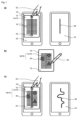
- Figure 1a shows an embodiment of the device (10) of the proposed system, in which the electrically conductive basic structure (14) is arranged on the substrate material (12) and comprises a plurality of individual elements (16).
- a time-dependent reference signal (28th ) generated in the form of a straight line, which is determined by the arrangement, electrical conductivity, shape, size and spacing of the individual elements (16).
- Figure 1b shows the subsequent local application of a second electrically conductive layer (40) using a pen with electrically conductive ink (46).
- the second electrically conductive layer (40) or structure which at least partially overlaps the electrically conductive base structure (14), creates a new resulting electrically conductive structure (18) on the device (10).
- the electrically conductive basic structure (14) and the second electrically conductive structure (18) are referred to as a generic term with the term "electrically conductive structure (70)".
- the resulting electrically conductive structure (18) generates a modified signal (30) on the capacitive area sensor (24) in comparison to the reference signal (28) through a dynamic input (22) using input means (20) ( Figure 1c ).
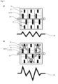
- Figure 2a shows a preferred embodiment of the device (10) of the proposed system with a regular electrically conductive basic structure (14), arranged on a substrate (12) and comprising several individual elements (16).
- this basic structure With dynamic input (22) by means of input means (not shown) on the capacitive area sensor (not shown), this basic structure generates a time-dependent reference signal (28) which reflects this regularity.
- Figure 2b shows additional exemplary electrically conductive markings in the form of crosses (40), which can be subsequently applied by an electrically conductive pen (not shown) or another printing process.
- This second electrically conductive layer (40) at least partially overlaps with the electrically conductive base structure (14).
- the resulting electrically conductive structure (18) determines a changed electrically conductive signal (30) on the capacitive area sensor.
- the insertion of the crosses with a pen with electrically conductive ink represents a subsequent change within the meaning of the invention, with which the electrically conductive basic structure (14) is converted into a second electrically conductive structure (18).
- the two different electrically conductive structures (14 and 18) each generate different electrical signals (28 and 30) on the surface sensor (not shown).
- Figure 3a shows a preferred embodiment of the device (10) of the proposed system with a regular electrically conductive basic structure (14) which is arranged on a web-like substrate material (12).
- the individual elements (16) of the electrically conductive structure are elements of the same geometry (shape) and size, which are arranged regularly and at the same distance from one another.
- the substrate material (12) in web or roll form with the electrically conductive basic structure (14) moves in the specified direction (22) relative to an inkjet printer (42) which is arranged above the moving substrate web (12).
- Additional electrically conductive material (40) is partially applied to the substrate (12) by means of the inkjet printer (42).
- the additionally applied electrically conductive material (40) at least partially overlaps the electrically conductive basic structure (14) and thus connects individual elements (16) of the electrically conductive basic structure (14) and thus produces the resulting electrically conductive layer (18).
- an electrically conductive basic structure (14) can subsequently be individualized or even serialized.
- the capacitive area sensor (24) is designed in such a way that one of the electrodes on the area sensor serves as input means (20). This electrode is marked with "S” in the drawing, which stands for transmitting electrode. The two other electrodes shown on the capacitive area sensor (24) are marked with "R", which stands for reader or reading electrode.
- the individualized resulting electrically conductive structure (18) is detected with the aid of the capacitive area sensor shown schematically.
- the duration of the resulting time-dependent signal (30) is determined by the duration of the unwinding.
- Figure 3b shows a similar embodiment of the device (10) of the proposed system, in which the subsequent application of electrically conductive material (40) takes place with the aid of a pen (46) or another suitable applicator, e.g. dispenser, and this applicator applies locally electrically conductive material ( 40), which at least partially overlaps the electrically conductive basic structure (14) and thus produces a resulting electrically conductive layer (18).
- the readout process using a capacitive area sensor (24) takes place analogously to the description in Figure 3a .ln figure 4 two different variants for the application of the additional electrically conductive material (40) on the substrate (12) with an already existing electrically conductive basic structure (14) are shown.
- Figure 4a shows an electrically conductive base structure (14) which is arranged on the substrate (12) of the device (10) of the proposed system.
- the device (10) and in particular the electrically conductive structure (70) is in active contact (26) with the capacitive area sensor (24).
- the input means (20) is moved in a relative movement (22) over the device (10) and in particular over the electrically conductive structure (14/70).
- a time-dependent signal (28) is generated on the capacitive area sensor (24).
- Figure 4b shows the additional applied electrically conductive material (40), which was applied directly to the electrically conductive base structure (14). This results in direct galvanic contact between the electrically conductive base structure (14) and additional electrically conductive material (40).
- the basic structure (14) is open, ie not covered, and the second electrically conductive layer (40) forms a galvanic connection with the first electrically conductive layer (14), ie individual elements of the basic structure (16) are electrically connected to one another or galvanically bridged.
- the resultant electrically conductive layer (18) thus produced generates a resultant time-dependent signal (30) on the capacitive area sensor (not shown), which preferably differs from the time-dependent reference signal (28).
- the electrically conductive basic structure (14) is covered, ie the first electrically conductive structure (14) is covered, for example, by an additional color or laminate layer (44).
- This additional layer can be a layer of lacquer and/or a layer of paint and/or an additional laminate material, for example paper or foil.
- the second electrically conductive layer (40) has a capacitive interaction with the first electrically conductive layer (14).
- Individual elements (16) can be connected to one another capacitively.
- the resulting electrically conductive structure (18) generates a signal (30) that differs from the reference signal (28) on the capacitive area sensor (not shown).
- FIG 5a a card-like object (10) with an electrically conductive structure (14) is shown.
- An electrically conductive cover structure (52, shown hatched) is partially located on this structure.
- the card (10 when placed on a capacitive area sensor (24, not shown), when a dynamic input is made by a user on the device using an input means (not shown), a time-dependent reference signal in the form of a straight line line (28).
- the Figure 5b shows the electrically conductive resulting structure (18) after the electrically conductive cover structure (52) has been removed.
- this card (10) generates a deflected time-dependent signal (30) when placed on a capacitive surface sensor and dynamic input on the device by an input means, as shown in the graphic.
- the arrow marks the movement (22) of an input device (not shown), such as a finger or a pen, on the card-like object or the device (10), in particular on the electrically conductive structure (70).
- a card-like object (10) is shown as part of the proposed system with an electrically conductive base structure (14).
- this card generates a time-dependent reference signal (28) in the form of a straight line when placed on a capacitive area sensor (not shown) and dynamic input (22) on the device (10) by an input means (not shown).
- the Figure 6b shows the resulting electrically conductive structure (18/70) after parts of the electrically conductive basic structure (14) have been removed.
- the interruptions in the electrically conductive structure (50) can be brought about, for example, by mechanical abrasion, for example with a scratch pen or eraser, or with a pen that contains a solvent that at least partially dissolves or destroys the electrically conductive base structure (14).
- this card is placed on a capacitive area sensor and dynamic input (22) is applied to the device (10), in particular the electrically conductive structure (18/70), an input means (not shown) generates a resulting deflected time-dependent signal (30 ), as shown in the graphic.
- Figure 7a represents a card-shaped object (10) as part of the proposed system with an electrically conductive basic structure (14/70).
- This electrically conductive basic structure (14) generates a time-dependent reference signal (28) on the capacitive area sensor (not shown).
- the substrate material (12) is provided with a perforation (60). After separating a section of the card-shaped object (10) along the perforation line, there are two parts of the card-shaped object (10a and 10b) with two different resulting electrically conductive structures (18a and 18b), each of which has changed resulting signals (30a and 30b) on the create a capacitive area sensor (not shown) ( Figure 7b and c ).
- Application examples of this embodiment of the device (10) include, for example, tickets that can be canceled by tearing them off.
- a further application example are labels or stickers for protecting documents, which separate along the perforation lines when attempting to remove or manipulate the label and thus determine a changed signal (30) on the capacitive area sensor (not shown).
- Such a label can also be used as protection against tampering or as a seal of originality for packaging.
- the electrically conductive structure (18) changed by the opening or manipulation process determines a changed time-dependent signal (30) on the surface sensor (not shown).
- Figure 8a shows an embodiment of the device (10) of the proposed system, in which the electrically conductive basic structure (14) is arranged on the substrate material (12) and comprises a plurality of individual elements (16).
- the dynamic Input (22) in the form of a linear swiping gesture represented by the arrow
- a time-dependent reference signal (28) is generated on the capacitive surface sensor (24), which is determined by the arrangement, electrical conductivity, shape, size and spacing of the individual elements (16) ( Figure 8b ).
- Figure 8c shows the electrically conductive basic structure (14) of this embodiment.
- the upper part of the electrically conductive basic structure (14) is designed in such a way that the dynamic signal (28, upper part) determined by this part of the electrically conductive structure on the surface sensor (24) enables the device (10) to be identified.
- the lower part of the electrically conductive basic structure (14) is in the form of a generic lattice structure, which in this state defines a dynamic signal (28, lower part) in the form of a straight line on the area sensor (24) ( Figure 8b ).
- Figure 8d shows a preferred embodiment of the device covered with a layer of lacquer or a laminate (44).
- the electrically conductive base structure (14) is covered by the cover layer or the laminate (44) and is represented in the graphic by a dashed line.
- Electrically conductive material (40) is subsequently applied locally to the top layer or the laminate (44) in a structured manner using a pen with electrically conductive ink (46).
- the electrically conductive basic structure (14) and the second electrically conductive layer (40) are therefore not galvanically connected, but have a capacitive interaction with one another.
- the electrically conductive material (40) is in the form of lettering or a signature and overlaps the lower area of the electrically conductive base structure (14).
- Figure 8e shows a preferred embodiment of the resulting electrically conductive structure (18) on the device.
- the electrically conductive basic structure (14) and the second electrically conductive structure (18) are referred to as a generic term with the term "electrically conductive structure (70)".
- the resulting electrically conductive structure (18) generates a modified signal (30) on the capacitive area sensor (24) in comparison to the reference signal (28) through a dynamic input (22) using input means (20).
- the changed signal (30) is in Figure 8f shown and changed in particular in the lower part of the signal compared to the reference signal (28).
Landscapes
- Engineering & Computer Science (AREA)
- Physics & Mathematics (AREA)
- General Physics & Mathematics (AREA)
- Theoretical Computer Science (AREA)
- Artificial Intelligence (AREA)
- Computer Vision & Pattern Recognition (AREA)
- Computer Networks & Wireless Communication (AREA)
- Computer Hardware Design (AREA)
- Microelectronics & Electronic Packaging (AREA)
- Position Input By Displaying (AREA)
- Measurement Of Length, Angles, Or The Like Using Electric Or Magnetic Means (AREA)
- Toys (AREA)
Claims (13)
- Dispositif de génération d'un signal variable dépendant du temps dans un capteur capacitif de superficie (24), dans lequel le dispositif comprend un appareil (10) et le capteur capacitif de superficie (24), dans lequel l'appareil (10) comprend une première structure électriquement conductrice (14),dans lequel la première structure électriquement conductrice (14) peut être convertie en une seconde structure électriquement conductrice (18) en modifiant la première structure électriquement conductrice (14),caractérisé en ce quela première structure électriquement conductrice (14) comprend au moins deux éléments individuels (16) séparés galvaniquement l'un de l'autre et est conçue pour, lorsqu'une entrée dynamique (22) est réalisée sous la forme d'un mouvement d'un moyen d'entrée (20) par un utilisateur sur la première structure électriquement conductrice (14), tandis que l'appareil est en contact actif avec le capteur capacitif de superficie, générer un premier signal dépendant du temps (28) sur le capteur capacitif de superficie (24), qui est déterminé par la disposition, la conductivité électrique, la taille, la distance et/ou la forme des éléments individuels (16) de la première structure électriquement conductrice (14) etdans lequel la seconde structure électriquement conductrice (18) comprend au moins deux éléments individuels (16) séparés galvaniquement l'un de l'autre et est configurée pour, lorsqu'une entrée dynamique (22) est réalisée sous la forme d'un mouvement du moyen d'entrée (20) sur la seconde structure électriquement conductrice (18), tandis que l'appareil est en contact actif avec le capteur capacitif de superficie, générer un second signal dépendant du temps (30) sur le capteur capacitif de superficie (24), qui est déterminé par la disposition, la conductivité électrique, la taille, la distance et/ou la forme des éléments individuels (16) de la seconde structure électriquement conductrice (18).
- Dispositif selon la revendication 1
caractérisé en ce que
le dispositif comprend un stylo qui est conçu pour effectuer des modifications dans la première structure électriquement conductrice (14), dans lequel le stylo est de préférence conçu pour appliquer un matériau électriquement conducteur (40), de manière davantage préférée sous la forme d'une encre électriquement conductrice, sur la première structure conductrice ou pour retirer sélectivement une partie de la première structure électriquement conductrice (14). - Dispositif selon l'une des revendications précédentes caractérisé en ce que
le dispositif est conçu de sorte que la modification de la première structure électriquement conductrice (14) peut être effectuée par une ou plusieurs des mesures suivantesa) l'application d'un matériau électriquement conducteur (40),b) le retrait sélectif d'une partie de la première structure électriquement conductrice (14),c) l'application d'un matériau conçu pour modifier les propriétés, notamment la conductivité électrique, de la première structure électriquement conductrice (14). - Dispositif selon une ou plusieurs des revendications précédentes
caractérisé en ce que
une individualisation de l'appareil (10) peut être effectuée en modifiant la première structure électriquement conductrice (14) par une ou plusieurs des mesures suivantes :a) l'application d'un matériau électriquement conducteur (40) avec un stylo à encre électriquement conductrice,b) l'impression avec un matériau électriquement conducteur (40) à l'aide du procédé d'impression à jet d'encre. - Dispositif selon une ou plusieurs des revendications précédentes
caractérisé en ce que
le capteur capacitif de superficie (24) est un écran tactile. - Dispositif selon une ou plusieurs des revendications 1 à 5 caractérisé en ce que
la division ou la séparation de la première structure électriquement conductrice (14) peut être effectuée ena) ouvrant un emballage ou déchirant une bande de contrôle oub) retirant une étiquette ou un marqueur qui se sépare ou se délamine en au moins deux parties lors du retrait. - Dispositif selon une ou plusieurs des revendications 3 ou 4 caractérisé en ce que
le matériau électriquement conducteur (40) comprend un matériau ayant une conductivité électrique variable dans le temps. - Dispositif selon une ou plusieurs des revendications 1 à 7 caractérisé en ce que
les éléments individuels (16) des structures électriquement conductrices (14, 18) sont dimensionnés en termes de taille, d'espacement et de forme de sorte qu'à tout moment pendant l'entrée dynamique (22) au moins deux éléments individuels (16) sont au moins partiellement en contact actif avec un moyen d'entrée (20), dans lequel l'entrée dynamique (22) est effectuée avec le moyen d'entrée (20). - Dispositif selon une ou plusieurs des revendications 1 à 8 caractérisé en ce que
l'entrée dynamique (22) peut être modulée en termes de position,
de vitesse, de direction, de forme, d'interruption du signal, de fréquence et/ou d'intensité du signal. - Dispositif selon une ou plusieurs des revendications 1 à 9 caractérisé en ce que
la première structure électriquement conductrice (14) et/ou la seconde structure électriquement conductrice (18) est présente sur un substrat électriquement non conducteur (12), dans lequel le substrat électriquement non conducteur (12) repose sur le capteur capacitif de superficie (24), tandis qu'un effleurement de la première structure électriquement conductrice (14) et/ou de la seconde structure électriquement conductrice (18) par le doigt d'un utilisateur en tant que moyen d'entrée est possible. - Procédé de génération d'un signal variable dépendant du temps sur un capteur de zone capacitif (24),
comprenant les étapes suivantes :a) la fourniture d'un appareil (10) comprenant une première structure électriquement conductrice (14) comprenant au moins deux éléments individuels (16) séparés galvaniquement l'un de l'autre,b) la modification de la première structure électriquement conductrice (14), de sorte qu'une seconde structure électriquement conductrice (18) comprenant au moins deux éléments individuels séparés galvaniquement (16) est obtenue,c) le placement de l'appareil (10) sur le capteur capacitif de superficie (24), dans lequel la seconde structure électriquement conductrice (18) est au moins partiellement en contact actif (26) avec le capteur capacitif de superficie (24),d) la réalisation de l'entrée dynamique (22) sous la forme d'un mouvement d'un moyen d'entrée (20) par un utilisateur sur la seconde structure électriquement conductrice (18) tandis que la seconde structure électriquement conductrice (18) est au moins partiellement en contact actif (26) avec le capteur capacitif de superficie (24), de sorte qu'un second signal dépendant du temps (30) est généré sur le capteur capacitif de superficie (24), qui est déterminé par une disposition spatiale, une conductivité électrique, une taille, une distance et/ou une forme des éléments individuels (16) de la seconde structure électriquement conductrice (18) sur l'appareil (10). - Procédé selon la revendication 11
comprenant en outre les étapes suivantes entre les étapes a) et b)a1) le placement de l'appareil (10) sur le capteur capacitif de superficie (24), dans lequel la première structure électriquement conductrice (14) est au moins partiellement en contact actif (26) avec le capteur capacitif de superficie (24)a2) la réalisation de l'entrée dynamique (22) sous la forme d'un mouvement d'un moyen d'entrée (20) par un utilisateur sur la première structure électriquement conductrice (14) tandis que la première structure électriquement conductrice (14) est au moins partiellement en contact actif (26) avec le capteur capacitif de superficie (24), de sorte qu'un premier signal dépendant du temps (28) est généré sur le capteur capacitif de superficie (24), qui est déterminé par une disposition spatiale, une conductivité électrique, une taille, une distance et/ou une forme des éléments individuels (16) de la première structure électriquement conductrice (18) sur l'appareil (10). - Procédé selon l'une des revendications 11 ou 12 caractérisé en ce que
la modification de la première structure électriquement conductrice (14) à l'étape b) est effectuée par une ou plusieurs des mesures suivantesa) l'application d'un matériau électriquement conducteur (40),b) le retrait sélectif d'une partie de la première structure électriquement conductrice (14),c) l'application d'un matériau conçu pour modifier les propriétés, notamment la conductivité électrique, de la première structure électriquement conductrice (14).
Applications Claiming Priority (3)
| Application Number | Priority Date | Filing Date | Title |
|---|---|---|---|
| EP17000166 | 2017-01-31 | ||
| EP17001505.1A EP3355235A1 (fr) | 2017-01-31 | 2017-09-05 | Dispositif et utilisation du dispositif de génération d'un signal variable dépendant du temps dans un capteur capacitif de superficie ainsi que structure électriquement conductrice |
| PCT/EP2018/000043 WO2018141477A1 (fr) | 2017-01-31 | 2018-01-31 | Système et procédé pour générer un signal variable en fonction du temps sur un capteur surfacique capacitif, et utilisation d'un stylet pour modifier une structure électroconductrice sur un dispositif |
Publications (2)
| Publication Number | Publication Date |
|---|---|
| EP3577594A1 EP3577594A1 (fr) | 2019-12-11 |
| EP3577594B1 true EP3577594B1 (fr) | 2023-08-09 |
Family
ID=58192032
Family Applications (2)
| Application Number | Title | Priority Date | Filing Date |
|---|---|---|---|
| EP17001505.1A Withdrawn EP3355235A1 (fr) | 2017-01-31 | 2017-09-05 | Dispositif et utilisation du dispositif de génération d'un signal variable dépendant du temps dans un capteur capacitif de superficie ainsi que structure électriquement conductrice |
| EP18711812.0A Active EP3577594B1 (fr) | 2017-01-31 | 2018-01-31 | Dispositif et utilisation du dispositif de génération d'un signal variable dépendant du temps dans un capteur capacitif de superficie |
Family Applications Before (1)
| Application Number | Title | Priority Date | Filing Date |
|---|---|---|---|
| EP17001505.1A Withdrawn EP3355235A1 (fr) | 2017-01-31 | 2017-09-05 | Dispositif et utilisation du dispositif de génération d'un signal variable dépendant du temps dans un capteur capacitif de superficie ainsi que structure électriquement conductrice |
Country Status (2)
| Country | Link |
|---|---|
| EP (2) | EP3355235A1 (fr) |
| WO (1) | WO2018141477A1 (fr) |
Families Citing this family (4)
| Publication number | Priority date | Publication date | Assignee | Title |
|---|---|---|---|---|
| EP3623914A1 (fr) * | 2018-09-17 | 2020-03-18 | Prismade Labs GmbH | Dispositif, son utilisation et système de génération d'un signal périodique sur un capteur superficiel capacitif |
| DE102021003493A1 (de) * | 2021-07-06 | 2023-01-12 | Giesecke+Devrient Currency Technology Gmbh | Sicherheitsdokument und Verfahren zur Herstellung eines Sicherheitsdokuments |
| EP4420890A1 (fr) | 2023-02-24 | 2024-08-28 | Hueck Folien Gesellschaft m.b.H. | Substrat doté d'une couche électroconductrice |
| EP4420889A1 (fr) | 2023-02-24 | 2024-08-28 | Hueck Folien Gesellschaft m.b.H. | Élément de sécurité comprenant une couche électroconductrice |
Family Cites Families (9)
| Publication number | Priority date | Publication date | Assignee | Title |
|---|---|---|---|---|
| DE1690334A1 (de) * | 1968-01-11 | 1971-05-13 | Telefunken Patent | Verfahren zur Anfertigung von Druckstockvorlagen |
| DE2612653A1 (de) * | 1976-03-25 | 1977-10-06 | Wolfgang Natus | Versuchsplatine fuer den aufbau einer elektronischen schaltung |
| US5621200A (en) * | 1994-06-22 | 1997-04-15 | Panda Eng., Inc. | Electronic verification machine for validating a medium having conductive material printed thereon |
| EP2088532A1 (fr) * | 2008-02-06 | 2009-08-12 | Sascha Voigt | Support de données plat |
| US10411759B2 (en) | 2010-06-11 | 2019-09-10 | Touchpac Holdings, Llc | System comprising a capacitive information carrier for acquiring information |
| BR112013006786A2 (pt) * | 2010-09-20 | 2019-09-24 | Printechnologics Gmbh | portadora capacitiva de informação, método para produzir uma portadora capacitica de informação, sistema para a aquisição de informação e uso de uma portadora capacitiva de informação |
| EP2724761A1 (fr) | 2012-10-26 | 2014-04-30 | printechnologics GmbH | Objet modulaire pour l'identification par écran tactile |
| WO2014101912A1 (fr) | 2012-12-27 | 2014-07-03 | T-Touch International S.À.R.L. | Procédé d'identification capacitive d'un récipient comprenant un matériau électroconducteur |
| EP3002713A1 (fr) * | 2014-10-02 | 2016-04-06 | T-Touch International S.à.r.l. | Motif porteur d'information capacitif intégré à une impression d'illustrations de produit |
-
2017
- 2017-09-05 EP EP17001505.1A patent/EP3355235A1/fr not_active Withdrawn
-
2018
- 2018-01-31 EP EP18711812.0A patent/EP3577594B1/fr active Active
- 2018-01-31 WO PCT/EP2018/000043 patent/WO2018141477A1/fr not_active Ceased
Also Published As
| Publication number | Publication date |
|---|---|
| EP3577594A1 (fr) | 2019-12-11 |
| EP3355235A1 (fr) | 2018-08-01 |
| WO2018141477A1 (fr) | 2018-08-09 |
| WO2018141477A4 (fr) | 2018-10-04 |
| EP3355235A9 (fr) | 2019-03-20 |
Similar Documents
| Publication | Publication Date | Title |
|---|---|---|
| EP2353124B1 (fr) | Système d'identification et applications | |
| EP3577601B1 (fr) | Procédé de production d'un signal dépendant du temps sur un capteur de zone capacitif et procédé d'identification d'un objet de carte, et objet de carte et utilisation de celui-ci | |
| EP2580714B1 (fr) | Système doté d'un support d'informations capacitif servant à détecter des informations | |
| WO2010043422A1 (fr) | Support de données plat | |
| EP1615777B1 (fr) | Etiquette de securite et procede de fabrication associe | |
| EP1301355B1 (fr) | Papier de securite et valeur produite a partir dudit papier | |
| EP2635996B1 (fr) | Support d'informations et système pour détecter des informations | |
| EP2791768A1 (fr) | Support de données tactile et procédé | |
| EP2088532A1 (fr) | Support de données plat | |
| EP2721552A1 (fr) | Moyens de transmission de données unidirectionnelle ou bidirectionnelle | |
| WO2018141477A1 (fr) | Système et procédé pour générer un signal variable en fonction du temps sur un capteur surfacique capacitif, et utilisation d'un stylet pour modifier une structure électroconductrice sur un dispositif | |
| WO2020099477A1 (fr) | Procédé et dispositif pour une authentification multifacteur sur un capteur surfacique capacitif | |
| WO2012038490A1 (fr) | Support d'informations multiple | |
| EP2418607A1 (fr) | Support de données capacitif et système de saisie d'information | |
| EP2709800B1 (fr) | Procédé de fabrication d'un sceau de sécurité non détachable | |
| DE102008033461A1 (de) | Kartenförmiger Datenträger mit Sicherheitsmerkmal | |
| DE202010011032U1 (de) | Informationsträger und System zur Erfassung von Informationen | |
| EP3770819B1 (fr) | Couche porteuse et document de valeur ou de sécurité | |
| WO2006106020A1 (fr) | Etiquette a transpondeur | |
| EP3355246B1 (fr) | Procédé de production d'un signal dépendant du temps sur un capteur de zone capacitif et procédé d'identification d'un objet de carte, et objet de carte et utilisation de celui-ci | |
| EP4131190A1 (fr) | Détection de motifs électroconducteurs continus et répétitifs à l'aide des écrans tactiles capacitifs | |
| DE202008015342U1 (de) | Datenträger sowie Anwendungen | |
| DE202019102004U1 (de) | System zur Verifizierung von Dokumenten |
Legal Events
| Date | Code | Title | Description |
|---|---|---|---|
| STAA | Information on the status of an ep patent application or granted ep patent |
Free format text: STATUS: UNKNOWN |
|
| STAA | Information on the status of an ep patent application or granted ep patent |
Free format text: STATUS: THE INTERNATIONAL PUBLICATION HAS BEEN MADE |
|
| PUAI | Public reference made under article 153(3) epc to a published international application that has entered the european phase |
Free format text: ORIGINAL CODE: 0009012 |
|
| STAA | Information on the status of an ep patent application or granted ep patent |
Free format text: STATUS: REQUEST FOR EXAMINATION WAS MADE |
|
| 17P | Request for examination filed |
Effective date: 20190822 |
|
| AK | Designated contracting states |
Kind code of ref document: A1 Designated state(s): AL AT BE BG CH CY CZ DE DK EE ES FI FR GB GR HR HU IE IS IT LI LT LU LV MC MK MT NL NO PL PT RO RS SE SI SK SM TR |
|
| AX | Request for extension of the european patent |
Extension state: BA ME |
|
| RIN1 | Information on inventor provided before grant (corrected) |
Inventor name: THIELE, JAN Inventor name: WEIGELT, KARIN |
|
| RIN1 | Information on inventor provided before grant (corrected) |
Inventor name: THIELE, JAN Inventor name: WEIGELT, KARIN |
|
| DAV | Request for validation of the european patent (deleted) | ||
| DAX | Request for extension of the european patent (deleted) | ||
| STAA | Information on the status of an ep patent application or granted ep patent |
Free format text: STATUS: EXAMINATION IS IN PROGRESS |
|
| 17Q | First examination report despatched |
Effective date: 20200603 |
|
| GRAP | Despatch of communication of intention to grant a patent |
Free format text: ORIGINAL CODE: EPIDOSNIGR1 |
|
| STAA | Information on the status of an ep patent application or granted ep patent |
Free format text: STATUS: GRANT OF PATENT IS INTENDED |
|
| INTG | Intention to grant announced |
Effective date: 20230307 |
|
| GRAS | Grant fee paid |
Free format text: ORIGINAL CODE: EPIDOSNIGR3 |
|
| GRAA | (expected) grant |
Free format text: ORIGINAL CODE: 0009210 |
|
| STAA | Information on the status of an ep patent application or granted ep patent |
Free format text: STATUS: THE PATENT HAS BEEN GRANTED |
|
| AK | Designated contracting states |
Kind code of ref document: B1 Designated state(s): AL AT BE BG CH CY CZ DE DK EE ES FI FR GB GR HR HU IE IS IT LI LT LU LV MC MK MT NL NO PL PT RO RS SE SI SK SM TR |
|
| REG | Reference to a national code |
Ref country code: GB Ref legal event code: FG4D Free format text: NOT ENGLISH |
|
| REG | Reference to a national code |
Ref country code: CH Ref legal event code: EP |
|
| REG | Reference to a national code |
Ref country code: IE Ref legal event code: FG4D Free format text: LANGUAGE OF EP DOCUMENT: GERMAN |
|
| REG | Reference to a national code |
Ref country code: DE Ref legal event code: R096 Ref document number: 502018012925 Country of ref document: DE |
|
| REG | Reference to a national code |
Ref country code: LT Ref legal event code: MG9D |
|
| REG | Reference to a national code |
Ref country code: NL Ref legal event code: MP Effective date: 20230809 |
|
| PG25 | Lapsed in a contracting state [announced via postgrant information from national office to epo] |
Ref country code: GR Free format text: LAPSE BECAUSE OF FAILURE TO SUBMIT A TRANSLATION OF THE DESCRIPTION OR TO PAY THE FEE WITHIN THE PRESCRIBED TIME-LIMIT Effective date: 20231110 |
|
| PG25 | Lapsed in a contracting state [announced via postgrant information from national office to epo] |
Ref country code: IS Free format text: LAPSE BECAUSE OF FAILURE TO SUBMIT A TRANSLATION OF THE DESCRIPTION OR TO PAY THE FEE WITHIN THE PRESCRIBED TIME-LIMIT Effective date: 20231209 |
|
| PG25 | Lapsed in a contracting state [announced via postgrant information from national office to epo] |
Ref country code: SE Free format text: LAPSE BECAUSE OF FAILURE TO SUBMIT A TRANSLATION OF THE DESCRIPTION OR TO PAY THE FEE WITHIN THE PRESCRIBED TIME-LIMIT Effective date: 20230809 Ref country code: RS Free format text: LAPSE BECAUSE OF FAILURE TO SUBMIT A TRANSLATION OF THE DESCRIPTION OR TO PAY THE FEE WITHIN THE PRESCRIBED TIME-LIMIT Effective date: 20230809 Ref country code: PT Free format text: LAPSE BECAUSE OF FAILURE TO SUBMIT A TRANSLATION OF THE DESCRIPTION OR TO PAY THE FEE WITHIN THE PRESCRIBED TIME-LIMIT Effective date: 20231211 Ref country code: NO Free format text: LAPSE BECAUSE OF FAILURE TO SUBMIT A TRANSLATION OF THE DESCRIPTION OR TO PAY THE FEE WITHIN THE PRESCRIBED TIME-LIMIT Effective date: 20231109 Ref country code: NL Free format text: LAPSE BECAUSE OF FAILURE TO SUBMIT A TRANSLATION OF THE DESCRIPTION OR TO PAY THE FEE WITHIN THE PRESCRIBED TIME-LIMIT Effective date: 20230809 Ref country code: LV Free format text: LAPSE BECAUSE OF FAILURE TO SUBMIT A TRANSLATION OF THE DESCRIPTION OR TO PAY THE FEE WITHIN THE PRESCRIBED TIME-LIMIT Effective date: 20230809 Ref country code: LT Free format text: LAPSE BECAUSE OF FAILURE TO SUBMIT A TRANSLATION OF THE DESCRIPTION OR TO PAY THE FEE WITHIN THE PRESCRIBED TIME-LIMIT Effective date: 20230809 Ref country code: IS Free format text: LAPSE BECAUSE OF FAILURE TO SUBMIT A TRANSLATION OF THE DESCRIPTION OR TO PAY THE FEE WITHIN THE PRESCRIBED TIME-LIMIT Effective date: 20231209 Ref country code: HR Free format text: LAPSE BECAUSE OF FAILURE TO SUBMIT A TRANSLATION OF THE DESCRIPTION OR TO PAY THE FEE WITHIN THE PRESCRIBED TIME-LIMIT Effective date: 20230809 Ref country code: GR Free format text: LAPSE BECAUSE OF FAILURE TO SUBMIT A TRANSLATION OF THE DESCRIPTION OR TO PAY THE FEE WITHIN THE PRESCRIBED TIME-LIMIT Effective date: 20231110 Ref country code: FI Free format text: LAPSE BECAUSE OF FAILURE TO SUBMIT A TRANSLATION OF THE DESCRIPTION OR TO PAY THE FEE WITHIN THE PRESCRIBED TIME-LIMIT Effective date: 20230809 |
|
| PG25 | Lapsed in a contracting state [announced via postgrant information from national office to epo] |
Ref country code: PL Free format text: LAPSE BECAUSE OF FAILURE TO SUBMIT A TRANSLATION OF THE DESCRIPTION OR TO PAY THE FEE WITHIN THE PRESCRIBED TIME-LIMIT Effective date: 20230809 |
|
| PG25 | Lapsed in a contracting state [announced via postgrant information from national office to epo] |
Ref country code: ES Free format text: LAPSE BECAUSE OF FAILURE TO SUBMIT A TRANSLATION OF THE DESCRIPTION OR TO PAY THE FEE WITHIN THE PRESCRIBED TIME-LIMIT Effective date: 20230809 |
|
| PG25 | Lapsed in a contracting state [announced via postgrant information from national office to epo] |
Ref country code: SM Free format text: LAPSE BECAUSE OF FAILURE TO SUBMIT A TRANSLATION OF THE DESCRIPTION OR TO PAY THE FEE WITHIN THE PRESCRIBED TIME-LIMIT Effective date: 20230809 Ref country code: RO Free format text: LAPSE BECAUSE OF FAILURE TO SUBMIT A TRANSLATION OF THE DESCRIPTION OR TO PAY THE FEE WITHIN THE PRESCRIBED TIME-LIMIT Effective date: 20230809 Ref country code: ES Free format text: LAPSE BECAUSE OF FAILURE TO SUBMIT A TRANSLATION OF THE DESCRIPTION OR TO PAY THE FEE WITHIN THE PRESCRIBED TIME-LIMIT Effective date: 20230809 Ref country code: EE Free format text: LAPSE BECAUSE OF FAILURE TO SUBMIT A TRANSLATION OF THE DESCRIPTION OR TO PAY THE FEE WITHIN THE PRESCRIBED TIME-LIMIT Effective date: 20230809 Ref country code: DK Free format text: LAPSE BECAUSE OF FAILURE TO SUBMIT A TRANSLATION OF THE DESCRIPTION OR TO PAY THE FEE WITHIN THE PRESCRIBED TIME-LIMIT Effective date: 20230809 Ref country code: CZ Free format text: LAPSE BECAUSE OF FAILURE TO SUBMIT A TRANSLATION OF THE DESCRIPTION OR TO PAY THE FEE WITHIN THE PRESCRIBED TIME-LIMIT Effective date: 20230809 Ref country code: SK Free format text: LAPSE BECAUSE OF FAILURE TO SUBMIT A TRANSLATION OF THE DESCRIPTION OR TO PAY THE FEE WITHIN THE PRESCRIBED TIME-LIMIT Effective date: 20230809 |
|
| REG | Reference to a national code |
Ref country code: DE Ref legal event code: R097 Ref document number: 502018012925 Country of ref document: DE |
|
| PG25 | Lapsed in a contracting state [announced via postgrant information from national office to epo] |
Ref country code: IT Free format text: LAPSE BECAUSE OF FAILURE TO SUBMIT A TRANSLATION OF THE DESCRIPTION OR TO PAY THE FEE WITHIN THE PRESCRIBED TIME-LIMIT Effective date: 20230809 |
|
| PLBE | No opposition filed within time limit |
Free format text: ORIGINAL CODE: 0009261 |
|
| STAA | Information on the status of an ep patent application or granted ep patent |
Free format text: STATUS: NO OPPOSITION FILED WITHIN TIME LIMIT |
|
| 26N | No opposition filed |
Effective date: 20240513 |
|
| PG25 | Lapsed in a contracting state [announced via postgrant information from national office to epo] |
Ref country code: SI Free format text: LAPSE BECAUSE OF FAILURE TO SUBMIT A TRANSLATION OF THE DESCRIPTION OR TO PAY THE FEE WITHIN THE PRESCRIBED TIME-LIMIT Effective date: 20230809 |
|
| REG | Reference to a national code |
Ref country code: DE Ref legal event code: R119 Ref document number: 502018012925 Country of ref document: DE |
|
| PG25 | Lapsed in a contracting state [announced via postgrant information from national office to epo] |
Ref country code: MC Free format text: LAPSE BECAUSE OF FAILURE TO SUBMIT A TRANSLATION OF THE DESCRIPTION OR TO PAY THE FEE WITHIN THE PRESCRIBED TIME-LIMIT Effective date: 20230809 |
|
| PG25 | Lapsed in a contracting state [announced via postgrant information from national office to epo] |
Ref country code: MC Free format text: LAPSE BECAUSE OF FAILURE TO SUBMIT A TRANSLATION OF THE DESCRIPTION OR TO PAY THE FEE WITHIN THE PRESCRIBED TIME-LIMIT Effective date: 20230809 |
|
| REG | Reference to a national code |
Ref country code: CH Ref legal event code: PL |
|
| PG25 | Lapsed in a contracting state [announced via postgrant information from national office to epo] |
Ref country code: LU Free format text: LAPSE BECAUSE OF NON-PAYMENT OF DUE FEES Effective date: 20240131 |
|
| GBPC | Gb: european patent ceased through non-payment of renewal fee |
Effective date: 20240131 |
|
| PG25 | Lapsed in a contracting state [announced via postgrant information from national office to epo] |
Ref country code: LU Free format text: LAPSE BECAUSE OF NON-PAYMENT OF DUE FEES Effective date: 20240131 |
|
| PG25 | Lapsed in a contracting state [announced via postgrant information from national office to epo] |
Ref country code: DE Free format text: LAPSE BECAUSE OF NON-PAYMENT OF DUE FEES Effective date: 20240801 |
|
| PG25 | Lapsed in a contracting state [announced via postgrant information from national office to epo] |
Ref country code: GB Free format text: LAPSE BECAUSE OF NON-PAYMENT OF DUE FEES Effective date: 20240131 |
|
| PG25 | Lapsed in a contracting state [announced via postgrant information from national office to epo] |
Ref country code: BE Free format text: LAPSE BECAUSE OF NON-PAYMENT OF DUE FEES Effective date: 20240131 |
|
| PG25 | Lapsed in a contracting state [announced via postgrant information from national office to epo] |
Ref country code: FR Free format text: LAPSE BECAUSE OF NON-PAYMENT OF DUE FEES Effective date: 20240131 |
|
| PG25 | Lapsed in a contracting state [announced via postgrant information from national office to epo] |
Ref country code: CH Free format text: LAPSE BECAUSE OF NON-PAYMENT OF DUE FEES Effective date: 20240131 |
|
| PG25 | Lapsed in a contracting state [announced via postgrant information from national office to epo] |
Ref country code: GB Free format text: LAPSE BECAUSE OF NON-PAYMENT OF DUE FEES Effective date: 20240131 Ref country code: FR Free format text: LAPSE BECAUSE OF NON-PAYMENT OF DUE FEES Effective date: 20240131 Ref country code: DE Free format text: LAPSE BECAUSE OF NON-PAYMENT OF DUE FEES Effective date: 20240801 Ref country code: CH Free format text: LAPSE BECAUSE OF NON-PAYMENT OF DUE FEES Effective date: 20240131 Ref country code: BE Free format text: LAPSE BECAUSE OF NON-PAYMENT OF DUE FEES Effective date: 20240131 |
|
| REG | Reference to a national code |
Ref country code: BE Ref legal event code: MM Effective date: 20240131 |
|
| PG25 | Lapsed in a contracting state [announced via postgrant information from national office to epo] |
Ref country code: BG Free format text: LAPSE BECAUSE OF FAILURE TO SUBMIT A TRANSLATION OF THE DESCRIPTION OR TO PAY THE FEE WITHIN THE PRESCRIBED TIME-LIMIT Effective date: 20230809 |
|
| PG25 | Lapsed in a contracting state [announced via postgrant information from national office to epo] |
Ref country code: BG Free format text: LAPSE BECAUSE OF FAILURE TO SUBMIT A TRANSLATION OF THE DESCRIPTION OR TO PAY THE FEE WITHIN THE PRESCRIBED TIME-LIMIT Effective date: 20230809 |
|
| PG25 | Lapsed in a contracting state [announced via postgrant information from national office to epo] |
Ref country code: IE Free format text: LAPSE BECAUSE OF NON-PAYMENT OF DUE FEES Effective date: 20240131 |
|
| PG25 | Lapsed in a contracting state [announced via postgrant information from national office to epo] |
Ref country code: IE Free format text: LAPSE BECAUSE OF NON-PAYMENT OF DUE FEES Effective date: 20240131 |
|
| REG | Reference to a national code |
Ref country code: AT Ref legal event code: MM01 Ref document number: 1598338 Country of ref document: AT Kind code of ref document: T Effective date: 20240131 |
|
| PG25 | Lapsed in a contracting state [announced via postgrant information from national office to epo] |
Ref country code: AT Free format text: LAPSE BECAUSE OF NON-PAYMENT OF DUE FEES Effective date: 20240131 |
|
| PG25 | Lapsed in a contracting state [announced via postgrant information from national office to epo] |
Ref country code: CY Free format text: LAPSE BECAUSE OF FAILURE TO SUBMIT A TRANSLATION OF THE DESCRIPTION OR TO PAY THE FEE WITHIN THE PRESCRIBED TIME-LIMIT; INVALID AB INITIO Effective date: 20180131 |
|
| PG25 | Lapsed in a contracting state [announced via postgrant information from national office to epo] |
Ref country code: HU Free format text: LAPSE BECAUSE OF FAILURE TO SUBMIT A TRANSLATION OF THE DESCRIPTION OR TO PAY THE FEE WITHIN THE PRESCRIBED TIME-LIMIT; INVALID AB INITIO Effective date: 20180131 |
|
| PG25 | Lapsed in a contracting state [announced via postgrant information from national office to epo] |
Ref country code: TR Free format text: LAPSE BECAUSE OF FAILURE TO SUBMIT A TRANSLATION OF THE DESCRIPTION OR TO PAY THE FEE WITHIN THE PRESCRIBED TIME-LIMIT Effective date: 20230809 |