EP3577757B1 - Über 90-grad konzentrierter und verteilter doherty-impedanzinverter - Google Patents
Über 90-grad konzentrierter und verteilter doherty-impedanzinverter Download PDFInfo
- Publication number
- EP3577757B1 EP3577757B1 EP17732555.2A EP17732555A EP3577757B1 EP 3577757 B1 EP3577757 B1 EP 3577757B1 EP 17732555 A EP17732555 A EP 17732555A EP 3577757 B1 EP3577757 B1 EP 3577757B1
- Authority
- EP
- European Patent Office
- Prior art keywords
- output
- amplifier
- impedance
- strip line
- approximately
- Prior art date
- Legal status (The legal status is an assumption and is not a legal conclusion. Google has not performed a legal analysis and makes no representation as to the accuracy of the status listed.)
- Active
Links
Images


Classifications
-
- H—ELECTRICITY
- H03—ELECTRONIC CIRCUITRY
- H03F—AMPLIFIERS
- H03F1/00—Details of amplifiers with only discharge tubes, only semiconductor devices or only unspecified devices as amplifying elements
- H03F1/02—Modifications of amplifiers to raise the efficiency, e.g. gliding Class A stages, use of an auxiliary oscillation
- H03F1/0205—Modifications of amplifiers to raise the efficiency, e.g. gliding Class A stages, use of an auxiliary oscillation in transistor amplifiers
- H03F1/0288—Modifications of amplifiers to raise the efficiency, e.g. gliding Class A stages, use of an auxiliary oscillation in transistor amplifiers using a main and one or several auxiliary peaking amplifiers whereby the load is connected to the main amplifier using an impedance inverter, e.g. Doherty amplifiers
-
- H—ELECTRICITY
- H03—ELECTRONIC CIRCUITRY
- H03F—AMPLIFIERS
- H03F1/00—Details of amplifiers with only discharge tubes, only semiconductor devices or only unspecified devices as amplifying elements
- H03F1/56—Modifications of input or output impedances, not otherwise provided for
- H03F1/565—Modifications of input or output impedances, not otherwise provided for using inductive elements
-
- H—ELECTRICITY
- H03—ELECTRONIC CIRCUITRY
- H03F—AMPLIFIERS
- H03F3/00—Amplifiers with only discharge tubes or only semiconductor devices as amplifying elements
- H03F3/189—High-frequency amplifiers, e.g. radio frequency amplifiers
- H03F3/19—High-frequency amplifiers, e.g. radio frequency amplifiers with semiconductor devices only
- H03F3/195—High-frequency amplifiers, e.g. radio frequency amplifiers with semiconductor devices only in integrated circuits
-
- H—ELECTRICITY
- H03—ELECTRONIC CIRCUITRY
- H03F—AMPLIFIERS
- H03F3/00—Amplifiers with only discharge tubes or only semiconductor devices as amplifying elements
- H03F3/20—Power amplifiers, e.g. Class B amplifiers, Class C amplifiers
- H03F3/24—Power amplifiers, e.g. Class B amplifiers, Class C amplifiers of transmitter output stages
- H03F3/245—Power amplifiers, e.g. Class B amplifiers, Class C amplifiers of transmitter output stages with semiconductor devices only
-
- H—ELECTRICITY
- H10—SEMICONDUCTOR DEVICES; ELECTRIC SOLID-STATE DEVICES NOT OTHERWISE PROVIDED FOR
- H10W—GENERIC PACKAGES, INTERCONNECTIONS, CONNECTORS OR OTHER CONSTRUCTIONAL DETAILS OF DEVICES COVERED BY CLASS H10
- H10W44/00—Electrical arrangements for controlling or matching impedance
- H10W44/20—Electrical arrangements for controlling or matching impedance at high-frequency [HF] or radio frequency [RF]
-
- H—ELECTRICITY
- H03—ELECTRONIC CIRCUITRY
- H03F—AMPLIFIERS
- H03F2200/00—Indexing scheme relating to amplifiers
- H03F2200/451—Indexing scheme relating to amplifiers the amplifier being a radio frequency amplifier
-
- H—ELECTRICITY
- H10—SEMICONDUCTOR DEVICES; ELECTRIC SOLID-STATE DEVICES NOT OTHERWISE PROVIDED FOR
- H10W—GENERIC PACKAGES, INTERCONNECTIONS, CONNECTORS OR OTHER CONSTRUCTIONAL DETAILS OF DEVICES COVERED BY CLASS H10
- H10W44/00—Electrical arrangements for controlling or matching impedance
- H10W44/20—Electrical arrangements for controlling or matching impedance at high-frequency [HF] or radio frequency [RF]
- H10W44/203—Electrical connections
- H10W44/206—Wires
-
- H—ELECTRICITY
- H10—SEMICONDUCTOR DEVICES; ELECTRIC SOLID-STATE DEVICES NOT OTHERWISE PROVIDED FOR
- H10W—GENERIC PACKAGES, INTERCONNECTIONS, CONNECTORS OR OTHER CONSTRUCTIONAL DETAILS OF DEVICES COVERED BY CLASS H10
- H10W44/00—Electrical arrangements for controlling or matching impedance
- H10W44/20—Electrical arrangements for controlling or matching impedance at high-frequency [HF] or radio frequency [RF]
- H10W44/226—Electrical arrangements for controlling or matching impedance at high-frequency [HF] or radio frequency [RF] for HF amplifiers
- H10W44/234—Arrangements for impedance matching
Definitions
- the technology relates to high-speed, high-power, broad-bandwidth, integrated amplifiers which may be constructed from gallium nitride transistors or transistors formed from other semiconductor materials.
- Gallium nitride semiconductor material has received appreciable attention in recent years because of its desirable electronic and electro-optical properties.
- GaN has a wide, direct bandgap of about 3.4 eV that corresponds to the blue wavelength region of the visible spectrum.
- LEDs Light-emitting diodes
- LDs laser diodes
- These devices can emit visible light ranging from the violet to red regions of the visible spectrum.
- GaN Because of its wide bandgap, GaN is more resistant to avalanche breakdown and can maintain electrical performance at higher temperatures than other semiconductors, such as silicon. GaN also has a higher carrier saturation velocity compared to silicon. Additionally, GaN has a Wurtzite crystal structure, is a very stable and hard material, has a high thermal conductivity, and has a much higher melting point than other conventional semiconductors such as silicon, germanium, and gallium arsenide. Accordingly, GaN is useful for high-speed, high-voltage, and high-power applications. For example, gallium-nitride materials are useful in semiconductor amplifiers for radio-frequency (RF) communications, radar, RF energy, and microwave applications.
- RF radio-frequency
- US2012/025915 relates to a Doherty amplifier.
- US2012/092074 relates to an apparatus and method for a switched capacitor architecture for multi-band Doherty power amplifiers.
- EP2806557 relates to a Doherty amplifier.
- WO2009/027916 relates to an integrated Doherty amplifier.
- EP2458730 relates to a radiofrequency amplifier.
- US4375054 relates to a suspended substrate - 3dB microwave quadrature coupler.
- the structures and methods relate to circuitry for combining amplified signals and impedance matching at the output of a modified Doherty amplifier. Rearranging the order of signal combining and impedance matching compared to conventional Doherty amplifiers and using an impedance inverter that comprises an integrated distributed inductive element in the form of a microstrip line can appreciably improve amplifier bandwidth and allow scalability of signal amplification to higher powers.
- GaN transistors As described above, amplifiers comprising gallium nitride (GaN) transistors are useful for high-speed, high-voltage, and high-power applications because of the favorable material properties of gallium nitride.
- transistors formed from other semiconductor materials such as gallium arsenide, silicon carbide, silicon germanium, etc., may be suitable for certain high-speed, high-voltage, and high-power applications.
- Technology areas in which GaN transistors are finding increasing use are radio-frequency (RF) communications and radar.
- RF communications for example, GaN transistors may be used in Doherty amplifiers at a base station to amplify data signals for wireless broadcasting within a cell covered by the base station.
- a Doherty amplifier 100 may comprise a main amplifier 132 and a peaking amplifier 138 arranged on parallel circuit branches.
- An input RF signal is split by a 90-degree coupler 110 that provides an in-phase attenuated signal to the main amplifier and an attenuated signal rotated by 90 degrees (typically delayed by 90°) to the peaking amplifier.
- an impedance inverter 150 that includes a compensating 90-degree rotation is used to recombine the two signals into a combined and amplified output RF signal.
- An output impedance-matching element 160 may be connected to the combining node to match the output impedance of the Doherty amplifier to the impedance of a load (not shown).
- Impedance-matching components 122, 124 may be placed before the main amplifier and peaking amplifier in a Doherty amplifier. These matching components may be used to match the impedances of the transmission lines from the 90-degree coupler 110 to the input impedances of the two amplifiers, so that signal reflections from the amplifiers are reduced or essentially eliminated. Additional impedance-matching components 142, 144 may be placed at the outputs of the main and peaking amplifiers to match impedances to the input of the impedance inverter 150 (which may be 50 ohms by design) and to the combining node 155. The impedance-matching components 142, 144 may comprise resistive, capacitive, and/or inductive circuit elements.
- the inventor has recognized and appreciated that there is a cost in bandwidth performance of a Doherty amplifier 100 when impedance-matching components 142, 144 are placed between the outputs of the main and peaking amplifiers 132, 138 and the impedance inverter 150 and combining node 155.
- the impedance-matching components 142, 144 add electrical path length between the two amplifiers so that it may not be possible for the impedance inverter 150 to employ only a 90-degree rotation to compensate for the phase rotation introduced by the 90° coupler.
- the impedance inverter 150 may need to operate with a phase rotation ⁇ that is an odd integer multiple of 90 degrees according to the following relation ⁇ ⁇ 2 n + 1 90 ° where n is an integer value of 1 or greater.
- the low-power circuit model represents a case when the peaking amplifier is off.
- the inventor has recognized and appreciated that when the peaking amplifier is off, a substantial impedance mismatch can occur between the output of the main amplifier 132 and the combining node 155 in the Doherty amplifier. Accordingly, the low-power operation may constrain the rated RF fractional bandwidth for a Doherty amplifier, e.g., a guaranteed bandwidth for all signal levels.
- the main amplifier 132 is represented as a first current source I m and the peaking amplifier 138 is represented as a second current source I p , which outputs no current.
- the impedance inverter 150 is modeled as a transmission line having a resistance R o and having an adjustable phase rotation, which can be set to an odd multiple of 90° at the center frequency of operation (2 GHz for this simulation).
- the load impedance is R o /2.
- the impedance of the peaking amplifier when off is given a value of 20R o .
- Simulations circuits and circuit elements described herein may be implemented using a software tool such as Advanced Design System (ADS) available from Keysight Technologies, Inc. of Santa Rosa, California.
- ADS Advanced Design System
- Other suitable software tools include, but are not limited to NI AWR Design Environment available from AWR Corporation of El Segundo, California and Sonnet ® software tools available from Sonnet Software of North Syracuse, New York.
- the frequency-response curves 310, 320, 330 plotted in the graph represent the scattering parameter S(1,1) evaluated looking from the output of the main amplifier 132 (e.g. the current source I m ) into the impedance inverter 150.
- the frequency-response curves represent an amount of signal reflected back to the main amplifier ( e . g ., voltage-to-standing-wave ratio) as a function of frequency.
- an RF fractional bandwidth ( ⁇ / ⁇ o ) for the amplifier may be determined from a frequency difference ⁇ between the -20 dB points on the frequency-response curves where the value of the back-reflected signal is at least 20 dB below the signal level input to the impedance inverter.
- the minimum allowable phase rotation by the impedance inverter 150 may be 270° due to the extra electrical path length added by the impedance-matching elements.
- the RF fractional bandwidth reduces to about 3%.
- Conventional Doherty amplifiers for RF communication systems typically operate with RF fractional bandwidths less than about 4 %.
- the RF fractional bandwidth could increase to over 17 % as indicated by the frequency-response curve 330.
- the inventor has recognized and appreciated that removing the impedance-matching elements 142, 144 before the impedance inverter 150 and combining node 155 allows a reduction in the compensating phase introduced by the impedance inverter to 90° or approximately 90°.
- the compensating phase angle is preferably 90°, in some cases the coupler 110 may impart a phase difference between 85° and 95°, which is compensated by the impedance inverter.
- FIG. 4 depicts an embodiment of a modified Doherty amplifier 400 in which signals from the main and peaking amplifiers are combined first, and then impedance is matched to a load after combining.
- impedance matching can be accomplished in an output impedance-matching element 420 located after the combining node 155.
- the combining node 155 may be located at the output of the peaking amplifier 138.
- An input to an impedance inverter 410 may connect directly to an output from the main amplifier 132.
- the impedance inverter 410 comprises a conductive strip line 510 (e . g ., a microstrip line) that extends a length L.
- the length L may extend between and along output drain bonding pads 533 of the main amplifier 132 and the peaking amplifier 138.
- the conductive strip line 510 may have a width W .
- the length of the conductive strip line may be between approximately 2 millimeters and approximately 6 millimeters, according to some embodiments, and may be selected to provide a desired inductance for the strip line 510.
- the width of the conductive strip line may be between approximately 100 microns and approximately 1000 microns, according to some embodiments, and may be selected to provide a desired inductance for the strip line.
- the conductive strip line is formed over a ground conductor or ground plane and separated from the ground conductor or ground plane by a dielectric material (not shown).
- the conductive strip line may not be formed over or adjacent to a ground plane. Instead, a ground plane may be removed from an area of a PCB at which the conductive strip line is patterned.
- the conductive strip line when implemented in the impedance inverter for RF signals, may comprise an integrated distributed impedance element which is essentially entirely inductive.
- the strip line may include some parasitic capacitance and resistance.
- the conductive strip line may be formed on a substrate 505, upon which an output impedance matching element 560 may be manufactured.
- the main amplifier 132 and the peaking amplifier 138 may be mounted adjacent to the substrate 505 and be on one or more separate dies.
- the conductive strip line 510 may be integrated onto a same substrate on which the main amplifier 132 and/or the peaking amplifier 138 are formed.
- the substrate 505 on which the conductive strip line is formed may comprise a printed circuit board in some embodiments, a high-frequency laminate capable of carrying signals at GHz frequencies in some embodiments, a ceramic, or a semiconductor.
- An example of a high-frequency laminate is laminate model RO4003 ® available from Rogers Corporation of Chandler, Arizona.
- an impedance inverter 410 may further include one or more amplifier output bond wires 520 that connect to a drain bond pad 533 of the main amplifier and the conductive strip line 510 near a first end of the strip line (e.g., located within about a first 1/3 of the length of the strip line). Additionally, there may be one or more amplifier output bond wires 520 connected between a drain bond pad of the peaking amplifier 138 and an opposing end of the conductive strip line 510.
- the output bond wires 520 may be arranged at essentially uniform spacing along the strip line in some embodiments, but may be arranged non-uniformly in other embodiments. The spacing between the bond wires may be between approximately 100 microns and approximately 800 microns.
- the bond wires 520 may be comprise gold or any other suitable conductor, may have a diameter between 20 microns and 80 microns, and may arc or extend over the substrate 505 and substrate 503 to a height between approximately 50 microns and approximately 250 microns.
- the output bond wires 520 comprise lumped inductive elements of the impedance inverter 410.
- Such bond wires are recognized in the field of RF electronics as "lumped inductors" having an inductance that is determined primarily by a length and diameter of the bond wire.
- bond wires 520 may not be used. Instead, conductive interconnects such a microstrip transmission lines or conductive traces may be used to connect the strip line 510 to outputs from the main and peaking amplifiers. In some implementations where the conductive strip line 510, main amplifier and/or peaking amplifier are integrated onto a same substrate, one or both drain bond pads 530 may be replaced with or subsumed into the conductive strip line 510, so that the inductance of the impedance inverter is essentially entirely a distributed inductance.
- a combining node of the Doherty amplifier 400 may be located at the drain bond pad 533 of the peaking amplifier 138.
- the impedance inverter 410 may comprise lumped inductive elements (for example, the main and peaking amplifier output bond wires 520) and an integrated distributed inductive element comprising the conductive strip line 510.
- the impedance inverter may include lumped capacitive elements, which may include the drain-to source capacitances of the main amplifier 132 and the peaking amplifier 138 and capacitance of the drain bond pads 533.
- the impedance inverter 410 may further include a small distributed capacitance of the conductive strip line 510.
- lumped capacitance elements may be added as shunts to the drain bond pads 533 and/or inductive strip line 510 to adjust an operating frequency of the Doherty amplifier to a desired value, or added in series to extend a length of the impedance inverter for higher power applications.
- an integrated, inductive strip line may comprise two separated strip lines 512 that are connected by a capacitor 580 ( e . g ., a surface mount capacitor) added in series between the two halves of the strip line, as depicted in FIG. 5C .
- This arrangement of two strip lines can extend the overall distance between the two amplifiers, allowing larger amplifiers 132, 138 and higher power capability, without adding more inductance.
- the added capacitance should be limited to avoid altering phase rotation in the impedance inverter beyond 95 degrees.
- output bond wires 550 connected between a drain bond pad 533 of the peaking amplifier 138 and an output impedance-matching element 560 of the Doherty amplifier.
- the output impedance-matching element 560 may comprise lumped and/or distributed impedance elements that are used to match an impedance from the drain bond pad 533 of the peaking amplifier 138 to a load impedance ( e . g ., 50 ohms) at a load plane 570.
- the main amplifier 132 and/or the peaking amplifier 138 may comprise a linear array of transistors having gate conductors 532, drain contacts 534, and source contacts 536 formed on a semiconductor substrate 503.
- the drain contacts 534 for an amplifier may connect to a drain bond pad 533, at which one or more output bond wires 520, 550 may be bonded.
- the active regions of the transistors may comprise gallium nitride, which is desirable for high-power, high-frequency amplification of RF signals as described above.
- gallium nitride refers to gallium nitride (GaN) and any of its alloys, such as aluminum gallium nitride (Al x Ga (1-x) N), indium gallium nitride (In y Ga (1-y) N), aluminum indium gallium nitride (Al x In y Ga (1-x-y) N), gallium arsenide phosporide nitride (GaAs x P y N (1-x-y) ), aluminum indium gallium arsenide phosporide nitride (Al x In y Ga (1-x-y) As a P b N (1-a-b) ), amongst others.
- the transistors may be formed from other semiconductor materials such as gallium arsenide, silicon carbide, silicon germanium, silicon, indium phosphide, etc. and the invention is not limited to gallium-nitride-based amplifier
- a benefit of a conductive strip line 510 in the impedance inverter as an inductive impedance element is that it can more readily allow for scalability of power of the Doherty amplifier 400 compared to lumped inductive elements only.
- the power-handling capability of a Doherty amplifier may be determined by the size of transistors in the main amplifier 132 and peaking amplifier 138. Power may be increased in a Doherty amplifier by increasing the number of transistors (gate conductors, drain contacts, and source contacts) along the linear array of transistors in the main amplifier and the peaking amplifier. However, increasing the number of transistors and length of the arrays can require additional amplifier output bond wires 520 between the two amplifiers and corresponding locations on the conductive strip line 510, and may require increasing the length of the strip line.
- amplifier output bond wires 520 and increased length of the strip line would normally increase the inductance of the impedance inverter 410.
- the inventor has recognized and appreciated that this increase in inductance may be offset by decreasing the inductance of the conductive strip line 510.
- Inductance of the strip line 510 may be decreased by increasing its width W .
- the distributed inductance of the strip line 510 may be tuned to a desired value. According to some embodiments, a total of the distributed inductance of the strip line may be between approximately 250 picoHenries and approximately 1.5 nanoHenries.
- the inductance of the strip line 510 may be decreased by increasing its width W and/or decreasing its length L. Conversely, the inductance of the strip line may be increased by decreasing its width W and/or increasing its length L . Such changes will also affect any capacitance and resistance of the strip line.
- the conductive strip line 510 comprises a tunable impedance element for the impedance inverter 410 that may be adjusted at the patterning stage of manufacture for a desired application. Accordingly, power of the Doherty amplifier 400 may be scaled while preserving an operating frequency and bandwidth performance of the Doherty amplifier 400. Such scalability would not be possible in a purely lumped-element impedance inverter where the drain bond pad 533 of the main amplifier 132 is wire bonded directly to the drain bond pad of the peaking amplifier 138.
- Adding length to the transistor arrays may also add electrical path length to the impedance inverter 410.
- the electrical path length can be increased until the phase rotation reaches approximately 90 degrees, though higher values ( e . g ., up to 95 degrees) may be possible in some cases where the coupler 110 provides a higher phase rotation than 90 degrees. Because the phase rotation for a physical path length will depend on frequency, lower-frequency devices may allow greater length extensions of the amplifier transistor arrays and therefore handle high powers.
- 5A should be capable of amplifying RF signals in frequency ranges between about 500 MHz and about 6 GHz to power levels between about 5 Watts and about 100 Watts at 500 MHz and between about 5 Watts and about 35 Watts at 6 GHz.
- the rated output power levels can be as high as between about 20 Watts and about 100 Watts at 500 MHz and between about 20 Watts and about 35 Watts at 6 GHz.
- the power capability of the Doherty amplifier 400 may be doubled.
- a second main amplifier 132 may be located on a side of the conductive strip line opposite the illustrated first main amplifier 132.
- the output impedance-matching element 560 may be rotated 90 degrees and mounted near the end of the conductive strip line 510 by the peaking amplifier 138.
- a second peaking amplifier 138 may be located on a side of the conductive strip line opposite the illustrated first peaking amplifier 138. Drain bond pads from the additional main and peaking amplifiers may be wire bonded to the conductive strip line. Additional bond wires may be connected at angles from the output impedance-matching element 560 to drain bond pads of the peaking amplifiers 138.
- the impedance inverter 410 was modeled using a lumped-equivalent model: a single lumped inductor and shunt capacitors arranged in a pi network connected between the main amplifier 132 and the peaking amplifier 138. The capacitors were connected as shunts on either side of the inductor. The value of the inductor was 1.04 nH. The values of the two capacitors were 1.99 pF, which represented a sum of the drain-to-source capacitances ( ⁇ 1.6 pF) and drain bond pad capacitance ( ⁇ 0.39 pF).
- the circuit arrangement was similar to that shown in FIG. 2 , except the impedance inverter 150 is replaced with the lumped pi network and the peaking current source I p is replaced with a resistance of 20R o .
- the value of R o was 22.9 ohms. This first simulation was carried out to analyze the feasibility of the Doherty amplifier 400 in which combining is carried out first before impedance matching.
- the values of a Doherty amplifier's operating frequency ⁇ o and inductance L s of the strip line 510 are constrained in part by amplifier design.
- an amplifier design may have a drain-to-source capacitance C ds , and be rated at a maximum drain-to-source current I max for an operating voltage V ds .
- the resistance R o at which maximum power may be transferred from the amplifier may be determined approximately from the following relation. R o ⁇ 2 V ds ⁇ V k / I max where V k is the knee voltage for the amplifier.
- the admittance of the shunt capacitance C sh (primarily determined by C ds , though it may include drain pad capacitance and any added capacitance) and the impedance of the impedance inverter's inductance L c (determined from the wire bonds 520 and strip line 510) match the corresponding admittance and impedance values of R o , which yields: R o ⁇ 1 / C sh ⁇ o R o ⁇ ⁇ o L c Since C ds is primarily determined by the amplifiers' design and may be the dominant capacitance, EQ. 3 roughly constrains the operating frequency of the amplifier, though it may be tuned downward by adding additional shunt capacitance. According to some embodiments, when the operating frequency is selected, the conductive strip line may be designed to provide inductance according to EQ. 4.
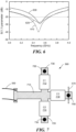
- a frequency-response curve 610 (dotted curve) from the first simulation with a lumped-element impedance inverter is plotted in FIG. 6 .
- the plot represents the scattering parameter S(1,1) looking into the impedance inverter ( e . g ., looking into the pi network at the first capacitive shunt).
- the response shows a bandwidth of about 400 MHz centered at an operating frequency of approximately 3.5 GHz. This bandwidth is greater than 11 % and represents a significant improvement over a comparable bandwidth performance of a conventional Doherty amplifier at RF frequencies, which is typically less than about 4 %.
- the lumped inductor was replaced with a distributed inductor that more accurately modeled the integrated conductive strip line 510 depicted in FIG. 5A .
- modeling of electromagnetic waves at different frequencies carried by the conductive strip line 510 was carried out using an electromagnetic (EM) field simulation tool.
- the conductive strip line was modeled as having six input ports corresponding to the bond wires 520. The input ports were 50 ⁇ m wide, with three spaced at each end on a 500 ⁇ m pitch. The length of the conductive strip line was 3.7 mm and the width was 300 ⁇ m.
- the conductive strip line was modeled as being formed from copper (17.5 ⁇ m thick) on a high-frequency laminate having a dielectric constant of 3.55 and a loss tangent of 0.002.
- the thickness of the laminate separating the conductive strip line from a ground plane was 305 ⁇ m.
- a mesh was used having 50 cells per wavelength at 4 GHz.
- the results from the EM simulation for the strip line 510 were used in a circuit simulation of the impedance inverter in which the same values of lumped capacitances (1.99 pF) were used and arranged in the pi network.
- the circuit arrangement was otherwise the same as that used to generate the frequency-response curve 610.
- results from this second simulation are plotted as the frequency-response curve 620 (dashed curve), which indicates that using a distributed inductive element in the impedance inverter adds minimal reduction in the RF fractional bandwidth compared to a purely lumped element impedance inverter. Accordingly, the inductive strip line 510 enables power scalability while essentially maintaining operating frequency and RF fractional bandwidth performance.
- Additional EM simulations were carried out to more accurately represent the output bonding pads 533 of the main amplifier 132 and peaking amplifier 138 as well as a circuit simulation to represent the bond wires 520 connected to the bonding pads 533.
- the bonding pads 533 measured approximately 1.8 mm by approximately 85 microns.
- the bond wires were represented as having a 25 micron diameter, a conductivity of 5 ⁇ 10 7 Siemens, extending over a gap of about 500 microns and rising to a maximal height of about 150 microns above the amplifier die.
- Using the results from the EM simulations in the circuit model for the Doherty amplifier 400 did not appreciably alter the frequency response curve 620.
- impedance at the output of the impedance inverter 410 may need to be matched to impedance of a load ( e . g ., 50 ohms).
- a load e . g . 50 ohms.
- an output impedance-matching element 560 was added to the circuit and simulations carried out to account for the added element.
- an output impedance-matching element 560 depicted in FIG. 7 was used, but the depicted element is only one example of an output-impedance matching element and the invention is not limited to only this configuration. Other embodiments may be used for the output-impedance-matching element in other implementations.
- output bond wires 550 are bonded to an output strip line 710 of the output impedance-matching element 560.
- Shunt capacitors 712, 714 connect between the output strip line 710 and pads 720, which are connected to an underlying ground conductor using a via and shunt conductor 730.
- An output capacitor 718 connects between the output strip line 710 and an output bonding pad 750.
- the output bonding pad 750 may be shunted to ground with a 50 ohm resistive via to emulate a load.
- the length and width of the output strip line 710, the values of the shunt capacitors 712, 714, and the value of the output capacitor 718 may be selected to match an impedance from the combining node to an impedance at the load plane 570.
- results of a simulation of amplifier performance that includes an output impedance-matching element 560 as arranged in FIG. 7 is plotted in FIG. 6 as the frequency-response curve 630.
- an impedance at the combining node (approximately 11.45 ohms) was matched to a load impedance of approximately 50 ohms.
- the strip line 710 measured approximately 1.4 mm in length with a width of approximately 350 microns, and otherwise used the same electromagnetic properties that were used for the conductive strip line 510.
- the shunt capacitors 712, 714 were modeled as surface-mount devices (SMDs) having a capacitance of 0.75 pF each.
- the shunt capacitors and conductive vias 730 had a combined resistance of 0.15 ohm and inductance of 0.3 nH each.
- the output capacitor 718 was also modeled as an SMD having a capacitance of 6.8 pF, which had a combined resistance of 0.15 ohm and inductance of 0.3 nH.
- the RF fractional bandwidth of the amplifier reduces to approximately 200 MHz or about 6% at an operating frequency of about 3.5 GHz. Even with this reduction, the RF fractional bandwidth for the modified Doherty amplifier is nearly twice the bandwidth of a conventional Doherty amplifier.
- the results of this simulation indicate that if the output impedance-matching is not done well, or has a narrow RF fractional bandwidth, then the overall bandwidth of the device may be limited by the output impedance-matching element 560.
- a double-section output impedance-matching element 800 is used, as depicted in FIG. 8 .
- a double-section impedance-matching element comprises an added inductive strip line 850 that connects to the output bonding pad 750 and to capacitive shunt 814.
- the dimensions of the strip line 710 may be resized to provide a desired inductance for the first section.
- Some embodiments may include transistor biasing components comprising an inductive strip line 840 that connects to a DC biasing port 830, at which voltage for biasing drains of transistors in the amplifiers 132, 138 may be applied.
- a shunt capacitor 816 may be connected to the biasing port 830.
- an additional capacitor may be mounted external to the board on which the impedance-matching element 800 is formed and arranged in parallel to the shunt capacitor 816.
- the external capacitor may have a value between 2 microFarads and 50 microFarads.
- the double-section impedance-matching element 800 provides improved impedance matching over a range of RF frequencies near the center or carrier frequency at 3.5 GHz, as compared to the single section depicted in FIG. 7 . Therefore, it removes a bandwidth bottleneck associated with the single section impedance-matching element 560 and recovers the RF fractional bandwidth available for the impedance inverter. The simulations show that the resulting RF fractional bandwidth recovers to approximately 18%.
- additional impedance-matching sections may be included between the impedance inverter and load.
- the double-section output impedance-matching element transforms the impedance at the output of the impedance inverter 410 to match or approximately match the impedance at the load plane 570 over a bandwidth of interest (e . g ., 80 MHz, 100 MHz, 200 Mhz, 400 MHz, or any desired RF fractional bandwidth in this range) at the carrier frequency (3.5 GHz in the above example, though other carrier frequencies may be used).
- a method for operating a Doherty amplifier 400 may comprise acts of splitting a received signal into a first signal and a second signal having a first phase with respect to the first signal, amplifying the first signal with a main amplifier 132, and amplifying the second signal with a peaking amplifier 138.
- a method embodiment may further comprise providing an output from the main amplifier directly to an input of an impedance inverter 410, wherein the impedance inverter comprises an integrated distributed inductor, and introducing a second phase with the impedance inverter that compensates for the first phase.
- a method for operating a Doherty amplifier may further comprise combining an output from the impedance inverter 410 with an output from the peaking amplifier 138 to produce a combined output, and providing the combined output to an impedance-matching element 560 that matches the output impedance to the impedance of a load.
- the terms “approximately” and “about” may be used to mean within ⁇ 20% of a target dimension in some embodiments, within ⁇ 10% of a target dimension in some embodiments, within ⁇ 5% of a target dimension in some embodiments, and yet within ⁇ 2% of a target dimension in some embodiments.
- the terms “approximately” and “about” may include the target dimension.
- the technology described herein may be embodied as a method, of which at least some acts have been described.
- the acts performed as part of the method may be ordered in any suitable way. Accordingly, embodiments may be constructed in which acts are performed in an order different than described, which may include performing some acts simultaneously, even though described as sequential acts in illustrative embodiments. Additionally, a method may include more acts than those described, in some embodiments, and fewer acts than those described in other embodiments.
Landscapes
- Engineering & Computer Science (AREA)
- Power Engineering (AREA)
- Microelectronics & Electronic Packaging (AREA)
- Amplifiers (AREA)
- Input Circuits Of Receivers And Coupling Of Receivers And Audio Equipment (AREA)
- General Induction Heating (AREA)
- Electrotherapy Devices (AREA)
- Microwave Amplifiers (AREA)
Claims (15)
- Ein Doherty-Verstärker, der Folgendes aufweist:einen Funk- bzw. HF-Eingang;einen Hauptverstärker (132), der mit dem HF-Eingang verbunden ist;einen Spitzenverstärker (138), der mit dem HF-Eingang verbunden ist;ein Kombinationsknoten (155), an dem sich ein Ausgang des Hauptverstärkers mit einem Ausgang des Spitzenverstärkes kombiniert, wobei der Kombinationsknoten sich an einem Drain-Bonding-Pad (533) des Spitzenverstärkers befindet;ein Impedanzinverter (150) aufweisend eine integrierte verteilte Induktivität, die zwischen einem Ausgang des Hauptverstärkers und dem Kombinationsknoten verbunden ist;ein Doppel-Sektionen Ausgangs-Impedanz-Anpassungselement (800) konfiguriert zum Anpassen einer Impedanz des Kombinationsknotens (155) an eine Impedanz einer Last-Ebene (570) an einem Ausgangs-Bonding-Pad (750) über eine Bandbreite von Interesse, wobei das Ausgangs-Impedanz-Anpassungselement (800) Folgendes aufweist, eine Ausgangs-Streifenleitung (710), erste und zweite Shunt-Kondensatoren (812, 814), die zwischen der Ausgangs-Streifenleitung (710) und Erde verbunden sind, einen Ausgangs-Kondensator (818), der zwischen der Ausgangs-Streifenleitung und dem Ausgangs-Bonding-Pad (750) verbunden ist, eine induktive Streifenleitung (850), die zwischen dem Ausgangs-Bonding-Pad (750) und Erde verbunden ist, und Ausgangs-Bonddrähte (550) konfiguriert zum Bonden der Ausgangs-Streifenleitung (710) mit dem Kombinationsknoten (155).
- Der Doherty-Verstärker nach Anspruch 1, wobei ein Eingang zum Impedanz-Inverter (150) einen oder mehrere Bonddrähte aufweist, die mit dem Ausgang des Hauptverstärkers (132) verbunden sind.
- Der Doherty-Verstärker nach Anspruch 1, wobei der Impedanz-Inverter (150) eine leitende Streifenleitung aufweist, die nicht über einer Erd-Ebene geformt ist.
- Der Doherty-Verstärker nach Anspruch 1, wobei es keine Impedanz-Anpassungselemente gibt, die zwischen dem Hauptverstärker (132) und dem Impedanz-Inverter (150) sind um eine Ausgangsimpedanz der Hauptverstärkers auf 50 Ohm anzupassen.
- Der Doherty-Verstärker nach einem der Ansprüche 1 bis 4, wobei die integrierte verteilte Induktivität eine leitende Streifenleitung aufweist mit einer Breite und Länge integriert auf einem Substrat.
- Der Doherty-Verstärker nach Anspruch 5, wobei der Impedanz-Inverter (150) ferner wenigstens ein kapazitives Element aufweist.
- Der Doherty-Verstärker nach Anspruch 5, wobei der Impedanz-Inverter (150) ferner Bonddrähte oder leitende Verbindungen aufweist, die zwischen der leitenden Streifenleitung und Ausgängen des Hauptverstärkers (132) und des Spitzenverstärkers (138) verbunden sind.
- Der Doherty-Verstärker nach einem der Ansprüche 5 bis 7, wobei die Breite zwischen ungefähr 100 Mikrometer und ungefähr 1000 Mikrometer liegt und wobei die Länge zwischen ungefähr 2 Millimeter und ungefähr 6 Millimeter liegt.
- Der Doherty-Verstärker nach einem der Ansprüche 1 bis 4, wobei einer oder beide aus dem Hauptverstärker (132) und dem Spitzenverstärker (138) Gallium-Nitrid-Transistoren aufweist.
- Der Doherty-Verstärker nach einem der Ansprüche 1 bis 4, wobei der Impedanz-Inverter (150) im Wesentlichen aus Folgendem besteht:eine leitende Streifenleitung mit einer Breite und Länge integriert auf einem Substrat;Bonddrähte, die zwischen der leitenden Streifenleitung und Ausgängen des Hauptverstärkers (132) und des Spitzenverstärkers (138) verbunden sind; undDrain-zu-Source Kapazitäten des Hauptverstärkers und des Spitzenverstärkers.
- Der Doherty-Verstärker nach einem der Ansprüche 1 bis 4, wobei:der zweite Shunt-Kondensator (814) zwischen der Ausgangs-Streifenleitung (710) und Erde über ein Via verbunden ist; unddie induktive Streifenleitung (850) zwischen dem Ausgangs-Bonding-Pad (750) und Erde über das Via verbunden ist.
- Der Doherty-Verstärker nach Anspruch 11, wobei eine HF-Teil-Bandbreite für den Verstärker zwischen ungefähr 6% und ungefähr 18% liegt und eine Betriebsfrequenz des Doherty-Verstärkers zwischen ungefähr 500 MHz und ungefähr 6 GHz liegt und ein Nenn-Ausgangs-Leistungsniveau des Kombinationsknotens zwischen ungefähr 20 Watt und ungefähr 100 Watt liegt.
- Der Doherty-Verstärker nach einem der Ansprüche 1 bis 12, der mit einem zellularen Transmitter verbunden ist.
- Ein Verfahren zum Verstärken von Signalen, das Folgendes aufweist:Splitten eines empfangenen Signals in ein erstes Signal und ein zweites Signal, das eine erste Phase in Bezug auf das erste Signal hat;Verstärken des ersten Signals mit einem Hauptverstärker (132);Verstärken des zweiten Signals mit einem Spitzenverstärker (138);Bereitstellen eines Ausgangs des Hauptverstärkers unmittelbar an einen Eingang eines Impedanz-Inverters (150), wobei der Impedanz-Inverter eine integrierte verteilte Induktivität aufweist;Einführen einer zweiten Phase, die die erste Phase kompensiert, mit dem Impedanz-Inverter;Kombinieren eines Ausgangs des Impedanz-Inverters mit einem Ausgang des Spitzenverstärkers an einem Kombinationsknoten (155), der sich an einem Drain-Bonding-Pad (533) des Spitzenverstärkers befindet, um einen kombinierten Ausgang zu erzeugen;Bereitstellen des kombinierten Ausgangs an ein Doppel-Sektionen Ausgangs-Impedanz-Anpassungselement (800) konfiguriert zum Anpassen einer Impedanz des Kombinationsknotens (155) an eine Impedanz einer Last-Ebene (570) an einem Ausgangs-Bonding-Pad (750) über eine Bandbreite von Interesse, wobei das Ausgangs-Impedanz-Anpassungselement (800) Folgendes aufweist, eine Ausgangs-Streifenleitung (710), erste und zweite Shunt-Kondensatoren (812, 814), die zwischen der Ausgangs-Streifenleitung (710) und Erde verbunden sind, einen Ausgangs-Kondensator (818), der zwischen der Ausgangs-Streifenleitung und dem Ausgangs-Bonding-Pad (750) verbunden ist, eine induktive Streifenleitung (850), die zwischen dem Ausgangs-Bonding-Pad (750) und Erde verbunden ist, und Ausgangs-Bonddrähte (550) konfiguriert zum Bonden der Ausgangs-Streifenleitung (710) mit dem Kombinationsknoten (155) .
- Das Verfahren nach Anspruch 14, wobei:der zweite Shunt-Kondensator (814) zwischen der Ausgangs-Streifenleitung (710) und Erde über ein Via verbunden ist; unddie induktive Streifenleitung (850) zwischen dem Ausgangs-Bonding-Pad (750) und Erde über das Via verbunden ist.
Applications Claiming Priority (1)
| Application Number | Priority Date | Filing Date | Title |
|---|---|---|---|
| PCT/IB2017/000727 WO2018142178A1 (en) | 2017-02-02 | 2017-02-02 | 90-degree lumped and distributed doherty impedance inverter |
Publications (2)
| Publication Number | Publication Date |
|---|---|
| EP3577757A1 EP3577757A1 (de) | 2019-12-11 |
| EP3577757B1 true EP3577757B1 (de) | 2024-12-18 |
Family
ID=59153224
Family Applications (1)
| Application Number | Title | Priority Date | Filing Date |
|---|---|---|---|
| EP17732555.2A Active EP3577757B1 (de) | 2017-02-02 | 2017-02-02 | Über 90-grad konzentrierter und verteilter doherty-impedanzinverter |
Country Status (3)
| Country | Link |
|---|---|
| EP (1) | EP3577757B1 (de) |
| TW (1) | TWI772360B (de) |
| WO (1) | WO2018142178A1 (de) |
Families Citing this family (12)
| Publication number | Priority date | Publication date | Assignee | Title |
|---|---|---|---|---|
| US11233483B2 (en) | 2017-02-02 | 2022-01-25 | Macom Technology Solutions Holdings, Inc. | 90-degree lumped and distributed Doherty impedance inverter |
| EP3616320B1 (de) | 2017-04-24 | 2023-11-08 | MACOM Technology Solutions Holdings, Inc. | Invertierter doherty-leistungsverstärker mit grossen hf- und momentanbandbreiten |
| US11159125B2 (en) | 2017-04-24 | 2021-10-26 | Macom Technology Solutions Holdings, Inc. | Inverted Doherty power amplifier with large RF fractional and instantaneous bandwidths |
| EP3616319A1 (de) | 2017-04-24 | 2020-03-04 | MACOM Technology Solutions Holdings, Inc. | Symmetrischer doherty-leistungsverstärker mit verbesserter effizienz |
| FR3070100A1 (fr) | 2017-08-14 | 2019-02-15 | Macom Technology Solutions Holdings, Inc. | Architecture d'amplificateur de puissance sans modulation, a large bande et a haut rendement |
| US11283410B2 (en) | 2017-10-02 | 2022-03-22 | Macom Technology Solutions Holdings, Inc. | No-load-modulation, high-efficiency power amplifier |
| CN112640298A (zh) | 2018-10-05 | 2021-04-09 | 镁可微波技术有限公司 | 低负载调制功率放大器 |
| JP2020170944A (ja) * | 2019-04-03 | 2020-10-15 | 株式会社村田製作所 | 高周波モジュール及び通信装置 |
| WO2021137951A1 (en) | 2019-12-30 | 2021-07-08 | Macom Technology Solutions Holdings, Inc. | Low-load-modulation broadband amplifier |
| US12028022B2 (en) | 2020-12-10 | 2024-07-02 | Macom Technology Solutions Holdings, Inc. | Hybrid power amplifier with GaN-on-Si and GaN-on-SiC circuits |
| JP7793898B2 (ja) * | 2021-06-21 | 2026-01-06 | 住友電気工業株式会社 | ドハティ増幅器 |
| CN117353260B (zh) * | 2023-11-02 | 2024-08-06 | 深圳市恒运昌真空技术股份有限公司 | 一种基于平衡功放的能量过冲抑制电路及其控制方法 |
Citations (2)
| Publication number | Priority date | Publication date | Assignee | Title |
|---|---|---|---|---|
| US4375054A (en) * | 1981-02-04 | 1983-02-22 | Rockwell International Corporation | Suspended substrate-3 dB microwave quadrature coupler |
| EP2458730B1 (de) * | 2010-11-29 | 2013-06-05 | NXP Semiconductors B.V. | Hochfrequenzverstärker |
Family Cites Families (8)
| Publication number | Priority date | Publication date | Assignee | Title |
|---|---|---|---|---|
| JP2005536922A (ja) * | 2002-08-19 | 2005-12-02 | コーニンクレッカ フィリップス エレクトロニクス エヌ ヴィ | 高出力ドハティ増幅器 |
| US8228123B2 (en) * | 2007-08-29 | 2012-07-24 | Nxp B.V. | Integrated Doherty amplifier |
| JP2012029239A (ja) * | 2010-07-27 | 2012-02-09 | Sumitomo Electric Device Innovations Inc | ドハティ増幅器 |
| US8576010B2 (en) * | 2010-10-19 | 2013-11-05 | Samsung Electronics Co., Ltd. | Apparatus and method for a switched capacitor architecture for multi-band doherty power amplifiers |
| EP2806557B1 (de) * | 2013-05-23 | 2017-03-08 | Ampleon Netherlands B.V. | Doherty-Verstärker |
| US9407214B2 (en) * | 2013-06-28 | 2016-08-02 | Cree, Inc. | MMIC power amplifier |
| US9800207B2 (en) * | 2014-08-13 | 2017-10-24 | Skyworks Solutions, Inc. | Doherty power amplifier combiner with tunable impedance termination circuit |
| US9748902B2 (en) * | 2015-05-15 | 2017-08-29 | Nxp Usa, Inc. | Phase correction in a Doherty power amplifier |
-
2017
- 2017-02-02 EP EP17732555.2A patent/EP3577757B1/de active Active
- 2017-02-02 WO PCT/IB2017/000727 patent/WO2018142178A1/en not_active Ceased
-
2018
- 2018-02-02 TW TW107103832A patent/TWI772360B/zh active
Patent Citations (2)
| Publication number | Priority date | Publication date | Assignee | Title |
|---|---|---|---|---|
| US4375054A (en) * | 1981-02-04 | 1983-02-22 | Rockwell International Corporation | Suspended substrate-3 dB microwave quadrature coupler |
| EP2458730B1 (de) * | 2010-11-29 | 2013-06-05 | NXP Semiconductors B.V. | Hochfrequenzverstärker |
Also Published As
| Publication number | Publication date |
|---|---|
| TW201836262A (zh) | 2018-10-01 |
| EP3577757A1 (de) | 2019-12-11 |
| TWI772360B (zh) | 2022-08-01 |
| WO2018142178A1 (en) | 2018-08-09 |
Similar Documents
| Publication | Publication Date | Title |
|---|---|---|
| US11722101B2 (en) | 90-degree lumped and distributed Doherty impedance inverter | |
| EP3577757B1 (de) | Über 90-grad konzentrierter und verteilter doherty-impedanzinverter | |
| US12381515B2 (en) | Symmetrical Doherty power amplifier having improved efficiency | |
| EP3577758B1 (de) | Über 90-grad konzentrierter und verteilter doherty-impedanzinverter | |
| WO2018142176A1 (en) | Methods for combining doherty amplifier signals with 90-degree lumped and distributed impedance inverters | |
| US11716058B2 (en) | No-load-modulation, high-efficiency power amplifier | |
| US11843352B2 (en) | Inverted Doherty power amplifier with large RF and instantaneous bandwidths | |
| US11990871B2 (en) | Inverted Doherty power amplifier with large RF fractional and instantaneous bandwidths | |
| CN113474992B (zh) | 具有宽带高频功率放大器特别是具有有源负载调制的N路Doherty放大器的传输和接收设备 |
Legal Events
| Date | Code | Title | Description |
|---|---|---|---|
| STAA | Information on the status of an ep patent application or granted ep patent |
Free format text: STATUS: UNKNOWN |
|
| STAA | Information on the status of an ep patent application or granted ep patent |
Free format text: STATUS: THE INTERNATIONAL PUBLICATION HAS BEEN MADE |
|
| PUAI | Public reference made under article 153(3) epc to a published international application that has entered the european phase |
Free format text: ORIGINAL CODE: 0009012 |
|
| STAA | Information on the status of an ep patent application or granted ep patent |
Free format text: STATUS: REQUEST FOR EXAMINATION WAS MADE |
|
| 17P | Request for examination filed |
Effective date: 20190829 |
|
| AK | Designated contracting states |
Kind code of ref document: A1 Designated state(s): AL AT BE BG CH CY CZ DE DK EE ES FI FR GB GR HR HU IE IS IT LI LT LU LV MC MK MT NL NO PL PT RO RS SE SI SK SM TR |
|
| AX | Request for extension of the european patent |
Extension state: BA ME |
|
| DAV | Request for validation of the european patent (deleted) | ||
| DAX | Request for extension of the european patent (deleted) | ||
| STAA | Information on the status of an ep patent application or granted ep patent |
Free format text: STATUS: EXAMINATION IS IN PROGRESS |
|
| 17Q | First examination report despatched |
Effective date: 20210811 |
|
| P01 | Opt-out of the competence of the unified patent court (upc) registered |
Effective date: 20230530 |
|
| GRAP | Despatch of communication of intention to grant a patent |
Free format text: ORIGINAL CODE: EPIDOSNIGR1 |
|
| STAA | Information on the status of an ep patent application or granted ep patent |
Free format text: STATUS: GRANT OF PATENT IS INTENDED |
|
| INTG | Intention to grant announced |
Effective date: 20240708 |
|
| GRAS | Grant fee paid |
Free format text: ORIGINAL CODE: EPIDOSNIGR3 |
|
| GRAA | (expected) grant |
Free format text: ORIGINAL CODE: 0009210 |
|
| STAA | Information on the status of an ep patent application or granted ep patent |
Free format text: STATUS: THE PATENT HAS BEEN GRANTED |
|
| AK | Designated contracting states |
Kind code of ref document: B1 Designated state(s): AL AT BE BG CH CY CZ DE DK EE ES FI FR GB GR HR HU IE IS IT LI LT LU LV MC MK MT NL NO PL PT RO RS SE SI SK SM TR |
|
| REG | Reference to a national code |
Ref country code: GB Ref legal event code: FG4D |
|
| REG | Reference to a national code |
Ref country code: CH Ref legal event code: EP |
|
| REG | Reference to a national code |
Ref country code: DE Ref legal event code: R096 Ref document number: 602017086821 Country of ref document: DE |
|
| REG | Reference to a national code |
Ref country code: IE Ref legal event code: FG4D |
|
| REG | Reference to a national code |
Ref country code: LT Ref legal event code: MG9D |
|
| PG25 | Lapsed in a contracting state [announced via postgrant information from national office to epo] |
Ref country code: HR Free format text: LAPSE BECAUSE OF FAILURE TO SUBMIT A TRANSLATION OF THE DESCRIPTION OR TO PAY THE FEE WITHIN THE PRESCRIBED TIME-LIMIT Effective date: 20241218 |
|
| PG25 | Lapsed in a contracting state [announced via postgrant information from national office to epo] |
Ref country code: FI Free format text: LAPSE BECAUSE OF FAILURE TO SUBMIT A TRANSLATION OF THE DESCRIPTION OR TO PAY THE FEE WITHIN THE PRESCRIBED TIME-LIMIT Effective date: 20241218 |
|
| PG25 | Lapsed in a contracting state [announced via postgrant information from national office to epo] |
Ref country code: BG Free format text: LAPSE BECAUSE OF FAILURE TO SUBMIT A TRANSLATION OF THE DESCRIPTION OR TO PAY THE FEE WITHIN THE PRESCRIBED TIME-LIMIT Effective date: 20241218 |
|
| PG25 | Lapsed in a contracting state [announced via postgrant information from national office to epo] |
Ref country code: NO Free format text: LAPSE BECAUSE OF FAILURE TO SUBMIT A TRANSLATION OF THE DESCRIPTION OR TO PAY THE FEE WITHIN THE PRESCRIBED TIME-LIMIT Effective date: 20250318 |
|
| REG | Reference to a national code |
Ref country code: NL Ref legal event code: MP Effective date: 20241218 |
|
| PG25 | Lapsed in a contracting state [announced via postgrant information from national office to epo] |
Ref country code: GR Free format text: LAPSE BECAUSE OF FAILURE TO SUBMIT A TRANSLATION OF THE DESCRIPTION OR TO PAY THE FEE WITHIN THE PRESCRIBED TIME-LIMIT Effective date: 20250319 Ref country code: LV Free format text: LAPSE BECAUSE OF FAILURE TO SUBMIT A TRANSLATION OF THE DESCRIPTION OR TO PAY THE FEE WITHIN THE PRESCRIBED TIME-LIMIT Effective date: 20241218 |
|
| PG25 | Lapsed in a contracting state [announced via postgrant information from national office to epo] |
Ref country code: RS Free format text: LAPSE BECAUSE OF FAILURE TO SUBMIT A TRANSLATION OF THE DESCRIPTION OR TO PAY THE FEE WITHIN THE PRESCRIBED TIME-LIMIT Effective date: 20250318 |
|
| PG25 | Lapsed in a contracting state [announced via postgrant information from national office to epo] |
Ref country code: NL Free format text: LAPSE BECAUSE OF FAILURE TO SUBMIT A TRANSLATION OF THE DESCRIPTION OR TO PAY THE FEE WITHIN THE PRESCRIBED TIME-LIMIT Effective date: 20241218 |
|
| REG | Reference to a national code |
Ref country code: AT Ref legal event code: MK05 Ref document number: 1753063 Country of ref document: AT Kind code of ref document: T Effective date: 20241218 |
|
| PG25 | Lapsed in a contracting state [announced via postgrant information from national office to epo] |
Ref country code: SM Free format text: LAPSE BECAUSE OF FAILURE TO SUBMIT A TRANSLATION OF THE DESCRIPTION OR TO PAY THE FEE WITHIN THE PRESCRIBED TIME-LIMIT Effective date: 20241218 |
|
| PG25 | Lapsed in a contracting state [announced via postgrant information from national office to epo] |
Ref country code: PL Free format text: LAPSE BECAUSE OF FAILURE TO SUBMIT A TRANSLATION OF THE DESCRIPTION OR TO PAY THE FEE WITHIN THE PRESCRIBED TIME-LIMIT Effective date: 20241218 |
|
| PG25 | Lapsed in a contracting state [announced via postgrant information from national office to epo] |
Ref country code: ES Free format text: LAPSE BECAUSE OF FAILURE TO SUBMIT A TRANSLATION OF THE DESCRIPTION OR TO PAY THE FEE WITHIN THE PRESCRIBED TIME-LIMIT Effective date: 20241218 |
|
| PG25 | Lapsed in a contracting state [announced via postgrant information from national office to epo] |
Ref country code: IS Free format text: LAPSE BECAUSE OF FAILURE TO SUBMIT A TRANSLATION OF THE DESCRIPTION OR TO PAY THE FEE WITHIN THE PRESCRIBED TIME-LIMIT Effective date: 20250418 |
|
| PG25 | Lapsed in a contracting state [announced via postgrant information from national office to epo] |
Ref country code: PT Free format text: LAPSE BECAUSE OF FAILURE TO SUBMIT A TRANSLATION OF THE DESCRIPTION OR TO PAY THE FEE WITHIN THE PRESCRIBED TIME-LIMIT Effective date: 20250421 |
|
| PG25 | Lapsed in a contracting state [announced via postgrant information from national office to epo] |
Ref country code: EE Free format text: LAPSE BECAUSE OF FAILURE TO SUBMIT A TRANSLATION OF THE DESCRIPTION OR TO PAY THE FEE WITHIN THE PRESCRIBED TIME-LIMIT Effective date: 20241218 |
|
| PG25 | Lapsed in a contracting state [announced via postgrant information from national office to epo] |
Ref country code: RO Free format text: LAPSE BECAUSE OF FAILURE TO SUBMIT A TRANSLATION OF THE DESCRIPTION OR TO PAY THE FEE WITHIN THE PRESCRIBED TIME-LIMIT Effective date: 20241218 Ref country code: AT Free format text: LAPSE BECAUSE OF FAILURE TO SUBMIT A TRANSLATION OF THE DESCRIPTION OR TO PAY THE FEE WITHIN THE PRESCRIBED TIME-LIMIT Effective date: 20241218 |
|
| PG25 | Lapsed in a contracting state [announced via postgrant information from national office to epo] |
Ref country code: SK Free format text: LAPSE BECAUSE OF FAILURE TO SUBMIT A TRANSLATION OF THE DESCRIPTION OR TO PAY THE FEE WITHIN THE PRESCRIBED TIME-LIMIT Effective date: 20241218 |
|
| PG25 | Lapsed in a contracting state [announced via postgrant information from national office to epo] |
Ref country code: CZ Free format text: LAPSE BECAUSE OF FAILURE TO SUBMIT A TRANSLATION OF THE DESCRIPTION OR TO PAY THE FEE WITHIN THE PRESCRIBED TIME-LIMIT Effective date: 20241218 |
|
| PG25 | Lapsed in a contracting state [announced via postgrant information from national office to epo] |
Ref country code: IT Free format text: LAPSE BECAUSE OF FAILURE TO SUBMIT A TRANSLATION OF THE DESCRIPTION OR TO PAY THE FEE WITHIN THE PRESCRIBED TIME-LIMIT Effective date: 20241218 |
|
| PG25 | Lapsed in a contracting state [announced via postgrant information from national office to epo] |
Ref country code: SE Free format text: LAPSE BECAUSE OF FAILURE TO SUBMIT A TRANSLATION OF THE DESCRIPTION OR TO PAY THE FEE WITHIN THE PRESCRIBED TIME-LIMIT Effective date: 20241218 |
|
| PG25 | Lapsed in a contracting state [announced via postgrant information from national office to epo] |
Ref country code: MC Free format text: LAPSE BECAUSE OF FAILURE TO SUBMIT A TRANSLATION OF THE DESCRIPTION OR TO PAY THE FEE WITHIN THE PRESCRIBED TIME-LIMIT Effective date: 20241218 |
|
| REG | Reference to a national code |
Ref country code: DE Ref legal event code: R097 Ref document number: 602017086821 Country of ref document: DE |
|
| REG | Reference to a national code |
Ref country code: CH Ref legal event code: PL |
|
| PG25 | Lapsed in a contracting state [announced via postgrant information from national office to epo] |
Ref country code: DK Free format text: LAPSE BECAUSE OF FAILURE TO SUBMIT A TRANSLATION OF THE DESCRIPTION OR TO PAY THE FEE WITHIN THE PRESCRIBED TIME-LIMIT Effective date: 20241218 |
|
| PG25 | Lapsed in a contracting state [announced via postgrant information from national office to epo] |
Ref country code: LU Free format text: LAPSE BECAUSE OF NON-PAYMENT OF DUE FEES Effective date: 20250202 |
|
| PG25 | Lapsed in a contracting state [announced via postgrant information from national office to epo] |
Ref country code: CH Free format text: LAPSE BECAUSE OF NON-PAYMENT OF DUE FEES Effective date: 20250228 |
|
| PLBE | No opposition filed within time limit |
Free format text: ORIGINAL CODE: 0009261 |
|
| STAA | Information on the status of an ep patent application or granted ep patent |
Free format text: STATUS: NO OPPOSITION FILED WITHIN TIME LIMIT |
|
| 26N | No opposition filed |
Effective date: 20250919 |
|
| GBPC | Gb: european patent ceased through non-payment of renewal fee |
Effective date: 20250318 |
|
| REG | Reference to a national code |
Ref country code: BE Ref legal event code: MM Effective date: 20250228 |
|
| PG25 | Lapsed in a contracting state [announced via postgrant information from national office to epo] |
Ref country code: GB Free format text: LAPSE BECAUSE OF NON-PAYMENT OF DUE FEES Effective date: 20250318 |
|
| PG25 | Lapsed in a contracting state [announced via postgrant information from national office to epo] |
Ref country code: BE Free format text: LAPSE BECAUSE OF NON-PAYMENT OF DUE FEES Effective date: 20250228 |
|
| PG25 | Lapsed in a contracting state [announced via postgrant information from national office to epo] |
Ref country code: IE Free format text: LAPSE BECAUSE OF NON-PAYMENT OF DUE FEES Effective date: 20250202 |
|
| PGFP | Annual fee paid to national office [announced via postgrant information from national office to epo] |
Ref country code: DE Payment date: 20260220 Year of fee payment: 10 |
|
| PGFP | Annual fee paid to national office [announced via postgrant information from national office to epo] |
Ref country code: FR Payment date: 20260224 Year of fee payment: 10 |