EP3579089A2 - Kraftsensor und anzeigevorrichtung damit - Google Patents
Kraftsensor und anzeigevorrichtung damit Download PDFInfo
- Publication number
- EP3579089A2 EP3579089A2 EP19174990.2A EP19174990A EP3579089A2 EP 3579089 A2 EP3579089 A2 EP 3579089A2 EP 19174990 A EP19174990 A EP 19174990A EP 3579089 A2 EP3579089 A2 EP 3579089A2
- Authority
- EP
- European Patent Office
- Prior art keywords
- force sensor
- electrode
- sensing
- force
- disposed
- Prior art date
- Legal status (The legal status is an assumption and is not a legal conclusion. Google has not performed a legal analysis and makes no representation as to the accuracy of the status listed.)
- Granted
Links
Images










Classifications
-
- G—PHYSICS
- G06—COMPUTING OR CALCULATING; COUNTING
- G06F—ELECTRIC DIGITAL DATA PROCESSING
- G06F3/00—Input arrangements for transferring data to be processed into a form capable of being handled by the computer; Output arrangements for transferring data from processing unit to output unit, e.g. interface arrangements
- G06F3/01—Input arrangements or combined input and output arrangements for interaction between user and computer
- G06F3/03—Arrangements for converting the position or the displacement of a member into a coded form
- G06F3/041—Digitisers, e.g. for touch screens or touch pads, characterised by the transducing means
- G06F3/0414—Digitisers, e.g. for touch screens or touch pads, characterised by the transducing means using force sensing means to determine a position
-
- G—PHYSICS
- G06—COMPUTING OR CALCULATING; COUNTING
- G06F—ELECTRIC DIGITAL DATA PROCESSING
- G06F3/00—Input arrangements for transferring data to be processed into a form capable of being handled by the computer; Output arrangements for transferring data from processing unit to output unit, e.g. interface arrangements
- G06F3/01—Input arrangements or combined input and output arrangements for interaction between user and computer
- G06F3/03—Arrangements for converting the position or the displacement of a member into a coded form
- G06F3/041—Digitisers, e.g. for touch screens or touch pads, characterised by the transducing means
- G06F3/0414—Digitisers, e.g. for touch screens or touch pads, characterised by the transducing means using force sensing means to determine a position
- G06F3/04142—Digitisers, e.g. for touch screens or touch pads, characterised by the transducing means using force sensing means to determine a position the force sensing means being located peripherally, e.g. disposed at the corners or at the side of a touch sensing plate
-
- G—PHYSICS
- G01—MEASURING; TESTING
- G01L—MEASURING FORCE, STRESS, TORQUE, WORK, MECHANICAL POWER, MECHANICAL EFFICIENCY, OR FLUID PRESSURE
- G01L1/00—Measuring force or stress, in general
- G01L1/20—Measuring force or stress, in general by measuring variations in ohmic resistance of solid materials or of electrically-conductive fluids; by making use of electrokinetic cells, i.e. liquid-containing cells wherein an electrical potential is produced or varied upon the application of stress
- G01L1/205—Measuring force or stress, in general by measuring variations in ohmic resistance of solid materials or of electrically-conductive fluids; by making use of electrokinetic cells, i.e. liquid-containing cells wherein an electrical potential is produced or varied upon the application of stress using distributed sensing elements
-
- G—PHYSICS
- G06—COMPUTING OR CALCULATING; COUNTING
- G06F—ELECTRIC DIGITAL DATA PROCESSING
- G06F1/00—Details not covered by groups G06F3/00 - G06F13/00 and G06F21/00
- G06F1/16—Constructional details or arrangements
- G06F1/1613—Constructional details or arrangements for portable computers
- G06F1/1633—Constructional details or arrangements of portable computers not specific to the type of enclosures covered by groups G06F1/1615 - G06F1/1626
- G06F1/1637—Details related to the display arrangement, including those related to the mounting of the display in the housing
- G06F1/1643—Details related to the display arrangement, including those related to the mounting of the display in the housing the display being associated to a digitizer, e.g. laptops that can be used as penpads
-
- G—PHYSICS
- G06—COMPUTING OR CALCULATING; COUNTING
- G06F—ELECTRIC DIGITAL DATA PROCESSING
- G06F1/00—Details not covered by groups G06F3/00 - G06F13/00 and G06F21/00
- G06F1/16—Constructional details or arrangements
- G06F1/1613—Constructional details or arrangements for portable computers
- G06F1/1633—Constructional details or arrangements of portable computers not specific to the type of enclosures covered by groups G06F1/1615 - G06F1/1626
- G06F1/1637—Details related to the display arrangement, including those related to the mounting of the display in the housing
- G06F1/1652—Details related to the display arrangement, including those related to the mounting of the display in the housing the display being flexible, e.g. mimicking a sheet of paper, or rollable
-
- G—PHYSICS
- G06—COMPUTING OR CALCULATING; COUNTING
- G06F—ELECTRIC DIGITAL DATA PROCESSING
- G06F1/00—Details not covered by groups G06F3/00 - G06F13/00 and G06F21/00
- G06F1/16—Constructional details or arrangements
- G06F1/1613—Constructional details or arrangements for portable computers
- G06F1/1633—Constructional details or arrangements of portable computers not specific to the type of enclosures covered by groups G06F1/1615 - G06F1/1626
- G06F1/1684—Constructional details or arrangements related to integrated I/O peripherals not covered by groups G06F1/1635 - G06F1/1675
- G06F1/169—Constructional details or arrangements related to integrated I/O peripherals not covered by groups G06F1/1635 - G06F1/1675 the I/O peripheral being an integrated pointing device, e.g. trackball in the palm rest area, mini-joystick integrated between keyboard keys, touch pads or touch stripes
-
- G—PHYSICS
- G06—COMPUTING OR CALCULATING; COUNTING
- G06F—ELECTRIC DIGITAL DATA PROCESSING
- G06F3/00—Input arrangements for transferring data to be processed into a form capable of being handled by the computer; Output arrangements for transferring data from processing unit to output unit, e.g. interface arrangements
- G06F3/01—Input arrangements or combined input and output arrangements for interaction between user and computer
- G06F3/03—Arrangements for converting the position or the displacement of a member into a coded form
- G06F3/041—Digitisers, e.g. for touch screens or touch pads, characterised by the transducing means
-
- G—PHYSICS
- G06—COMPUTING OR CALCULATING; COUNTING
- G06F—ELECTRIC DIGITAL DATA PROCESSING
- G06F3/00—Input arrangements for transferring data to be processed into a form capable of being handled by the computer; Output arrangements for transferring data from processing unit to output unit, e.g. interface arrangements
- G06F3/01—Input arrangements or combined input and output arrangements for interaction between user and computer
- G06F3/03—Arrangements for converting the position or the displacement of a member into a coded form
- G06F3/041—Digitisers, e.g. for touch screens or touch pads, characterised by the transducing means
- G06F3/0412—Digitisers structurally integrated in a display
-
- G—PHYSICS
- G06—COMPUTING OR CALCULATING; COUNTING
- G06F—ELECTRIC DIGITAL DATA PROCESSING
- G06F2203/00—Indexing scheme relating to G06F3/00 - G06F3/048
- G06F2203/041—Indexing scheme relating to G06F3/041 - G06F3/045
- G06F2203/04103—Manufacturing, i.e. details related to manufacturing processes specially suited for touch sensitive devices
-
- G—PHYSICS
- G06—COMPUTING OR CALCULATING; COUNTING
- G06F—ELECTRIC DIGITAL DATA PROCESSING
- G06F2203/00—Indexing scheme relating to G06F3/00 - G06F3/048
- G06F2203/041—Indexing scheme relating to G06F3/041 - G06F3/045
- G06F2203/04105—Pressure sensors for measuring the pressure or force exerted on the touch surface without providing the touch position
Definitions
- Exemplary embodiments of the present disclosure relate to a force sensor and a display device including the same.
- Electronic devices that provide images to a user include a display device that displays images.
- the display device includes a display panel that generates and displays an image, as well as various input devices such as a touch panel that recognizes a touch input. Due to the convenience of using a touch input method, the touch panel is replacing existing physical input devices such as physical buttons.
- Exemplary embodiments of the present disclosure provide a force sensor which can prevent a malfunction due to interference with other components and that enables convenient input, as well as a display device including the force sensor.
- a display device includes a display panel and a first force sensor.
- the first force sensor is disposed adjacent to a first edge of the display panel and extends along the first edge.
- the first force sensor comprises a plurality of first sensing regions and a second sensing region.
- the first sensing regions are disposed closer to a first end of the first force sensor than the second sensing region.
- the second sensing region is disposed closer to a second end of the first force sensor than the first sensing regions.
- the second sensing region has a wider area than each of the first sensing regions.
- a display device includes a display panel and a first force sensor.
- the first force sensor is disposed adjacent to a first edge of the display panel, extends along the first edge, and has a recess disposed at an inner side of the first force sensor.
- the first force sensor includes a plurality of first sensing regions and a second sensing region.
- the recess is disposed between the first sensing regions and the second sensing region.
- the second sensing region has a larger area than each of the first sensing regions.
- a force sensor includes a recess disposed at one side of the force sensor, a plurality of first sensing regions, and a second sensing region.
- the first sensing regions sense a first force.
- the second sensing region senses a second force.
- the recess is disposed between the first sensing regions and the second sensing region.
- the second sensing region has a larger area than each of the first sensing regions.
- a display device comprising: a display panel; and a first force sensor disposed adjacent to a first edge of the display panel, wherein the first force sensor extends along the first edge, wherein the first force sensor comprises a plurality of first sensing regions and a second sensing region, the first sensing regions disposed closer to a first end of the first force sensor than the second sensing region, and the second sensing region disposed closer to a second end of the first force sensor than the first sensing regions, wherein the second sensing region has a larger area than each of the first sensing regions.
- the first force sensor comprises a first electrode and a second electrode separated from the first electrode, wherein the first electrode is disposed over the first sensing regions and the second sensing region, and the second electrode is disposed separately in each of the first and second sensing regions.
- the first force sensor further comprises a force sensing layer comprising a force sensitive material having a resistance that varies according to a force, wherein the first electrode and the second electrode contact the force sensing layer.
- the first electrode comprises a first stem electrode and a plurality of first branch electrodes branching from the first stem electrode
- the second electrode comprises a second stem electrode and a plurality of second branch electrodes branching from the second stem electrode, wherein the first branch electrodes and the second branch electrodes are arranged alternately with each other.
- the first electrode is a driving electrode
- the second electrode is a sensing electrode
- the force sensing layer is disposed separately in each of the first and second sensing regions.
- a length of the second sensing region is about 30% to about 50% of a total length of the first force sensor.
- the display device further comprises: a second force sensor disposed adjacent to a second edge of the display panel, wherein the second edge faces the first edge and the second force sensor extends along the second edge, wherein the second force sensor comprises a plurality of third sensing regions and a fourth sensing region, the third sensing regions disposed closer to a first end of the second force sensor than the fourth sensing region, and the second sensing region disposed closer to a second end of the second force sensor than the third sensing regions, wherein the fourth sensing region has a larger area than each of the third sensing regions.
- the first sensing regions and the third sensing regions are pressing recognition regions
- the second sensing region and the fourth sensing region are squeezing recognition regions.
- the display device further comprises: a flat portion; a first curved portion connected to the flat portion; and a second curved portion connected to the flat portion, wherein the first curved portion is disposed at the first edge, the second curved portion is disposed at the second edge, the first force sensor is disposed in the first curved portion, and the second force sensor is disposed in the second curved portion.
- the first force sensor and the second force sensor are attached to a lower surface of the display panel.
- the display device further comprising: a bracket that houses the display panel, the first force sensor, and the second force sensor, wherein the first force sensor is attached to the bracket with a first waterproof tape, and the second force sensor is attached to the bracket with a second waterproof tape.
- a display device comprising: a display panel; and a first force sensor disposed adjacent to a first edge of the display panel, wherein the first force sensor extends along the first edge and comprises a recess disposed at an inner side of the first force sensor, wherein the first force sensor comprises a plurality of first sensing regions a second sensing region, wherein the recess is disposed between the first sensing regions and the second sensing region, and wherein the second sensing region has a larger area than each of the first sensing regions.
- the recess is notch-shaped.
- the first force sensor comprises a first electrode and a second electrode separated from the first electrode, wherein the first electrode is disposed over the first sensing regions and the second sensing region, and the second electrode is disposed separately in each of the first and second sensing regions.
- the first force sensor further comprises a force sensing layer comprising a force sensitive material having a resistance that varies according to a force, wherein the first electrode and the second electrode contact the force sensing layer.
- the first electrode comprises a first stem electrode and a plurality of first branch electrodes branching from the first stem electrode
- the second electrode comprises a second stem electrode and a plurality of second branch electrodes branching from the second stem electrode, wherein the first branch electrodes and the second branch electrodes are arranged alternately with each other.
- the first electrode is a driving electrode
- the second electrode is a sensing electrode
- the force sensing layer is disposed separately in each of the first and second sensing regions.
- a length of the second sensing region is about 30% to about 50% of a total length of the first force sensor.
- each first sensing region of the first force sensor is a pressing recognition region
- the second sensing region of the first force sensor is a squeezing recognition region
- the first force sensor comprises a first electrode formed as a single piece along a direction in which the first force sensor extends, and a second electrode formed as a single piece along the direction in which the first force sensor extends, wherein the second electrode is separated from the first electrode.
- the display device further comprises a touch member disposed on the display panel, wherein the touch member comprises a touch electrode overlapping the first force sensor.
- the display device further comprises a bracket that houses the display panel and the first force sensor, wherein the bracket comprises a connect hole through which a connector passes, and the recess bypasses the connect hole in an outward direction.
- the display device further comprises a second force sensor disposed adjacent to a second edge of the display panel that faces the first edge of the display panel.
- the second force sensor does not comprise the recess disposed in the first force sensor or any other recess.
- the second force sensor comprises a plurality of third sensing regions disposed between a first end of the second force sensor and a second end of the second force sensor, and a fourth sensing region disposed closer to the second end of the second force sensor than the third sensing regions, wherein the fourth sensing region has a wider area than each of the third sensing regions.
- a force sensor comprising: a recess disposed at one side of the force sensor; a plurality of first sensing regions that sense a first force; and a second sensing region that senses a second force, wherein the recess is disposed between the first sensing regions and the second sensing region, wherein the second sensing region has a larger area than each of the first sensing regions.
- the force sensor further comprises a first substrate comprising an electrode layer; and a second substrate that faces the first substrate and comprises a force sensing layer.
- the electrode layer comprises a first electrode and a second electrode separated from the first electrode, wherein the first electrode is disposed over the first sensing regions and the second sensing region, and the second electrode is disposed separately in each of the first and second sensing regions.
- the first electrode is a driving electrode
- the second electrode is a sensing electrode
- the first electrode and the second electrode are comb-shaped and engaged with each other.
- the force sensing layer comprises a force sensitive material having a resistance that varies according to a force, wherein the first electrode and the second electrode contact the force sensing layer.
- the force sensing layer is disposed separately in each of the first and second sensing regions.
- the force sensor further comprises: a bonding layer disposed between the first substrate and the second substrate along edges of the first substrate and the second substrate, wherein the bonding layer bonds the first substrate and the second substrate together and seals an internal space.
- a length of the second sensing region is about 30% to about 50% of a total length of the force sensor.
- first, second, etc. may be used herein to describe various elements, these elements should not be limited by these terms. These terms may be used to distinguish one element from another element. Thus, a first element discussed below may be termed a second element without departing from teachings of one or more exemplary embodiments. The description of an element as a “first” element may not require or imply the presence of a second element or other elements.
- the terms “first”, “second”, etc. may also be used herein to differentiate different categories or sets of elements. For conciseness, the terms “first”, “second”, etc. may represent “first-category (or first-set)", “second-category (or second-set)", etc., respectively.
- FIG. 1 is a perspective view of a display device 1 according to an exemplary embodiment.
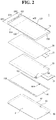
- FIG. 2 is an exploded perspective view of the display device 1 according to the exemplary embodiment of FIG. 1 .
- FIG. 3 is a cross-sectional view taken along line III-III' of FIG. 2 .
- the display device 1 includes a display panel 30 and force sensors 100 and 200 disposed near edges of the display panel 30.
- the display device 1 may further include a window 10 disposed above the display panel 30, a cover panel sheet 40 disposed below the display panel 30, and a bracket 50 (or a middle mold frame) disposed below the cover panel sheet 40.
- a bracket 50 or a middle mold frame
- the terms “above” and “upper surface” in a thickness direction denote a display surface side of the display panel 30, and the terms “below” and “lower surface” in the thickness direction, as used herein, denote an opposite side of the display panel 30 from the display surface side.
- the terms “above (upper),” “below (lower),” “left,” and “right” in a planar direction refer to directions when a display surface placed in position is viewed from above.
- the display device 1 may have a substantially rectangular shape in plan view.
- the display device 1 may have the shape of a rectangle with right-angled corners, or a rectangle with round corners in a plan view.
- the display device 1 may include long sides LS1 and LS2 and short sides SS1 and SS2.
- the long sides LS1 and LS2 are relatively longer than the short sides SS1 and SS2.
- a long side located on a right side in plan view will be referred to as a first long side LS1
- a long side located on a left side in a plan view will be referred to as a second long side LS2
- a short side located on an upper side in a plan view will be referred to as a first short side SS1
- a short side located on a lower side in a plan view will be referred to as a second short side SS2.
- the long sides LS1 and LS2 of the display device 1 may be, but embodiments are not limited to, about 1.5 to about 2.5 times longer than the short sides SS1 and SS2.
- the display device 1 may include a first area DR1 and a second area DR2 lying in different planes.
- the first area DR1 lies in a first plane.
- the second area DR2 is connected to the first area DR1, and is bent or curved from the first area DR1.
- the second area DR2 may lie in a second plane located at a predetermined crossing angle to the first plane or may have a curved surface.
- the second area DR2 of the display device 1 is disposed around the first area DR1.
- the first area DR1 of the display device 1 is used as a main display surface. Both the first area DR1 and the second area DR2 can be used as a display area of the display device 1.
- a case in which the first area DR1 of the display device 1 is a flat portion and the second area DR2 is a curved portion will be described below as an example.
- the second area DR2 which is the curved portion, may have a constant curvature or a varying curvature.
- the second area DR2 may be connected to the first area DR1.
- the second area DR2 may be disposed at edges of the display device 1.
- the second area DR2 may be disposed at both long edges (long sides LS1 and LS2) of the display device 1 which face each other.
- the second area DR2 may be disposed at one edge, at both short edges (short sides SS1 and SS2), at three edges, or at all edges of the display device 1.
- the display panel 30 is a panel for displaying an image and may be, for example, an organic light emitting diode (OLED) display panel.
- OLED organic light emitting diode
- a case in which an OLED display panel is applied as the display panel 30 will be described as an example.
- exemplary embodiments are not limited thereto, and other types of display panels such as, for example, a liquid crystal display (LCD) panel and an electrophoretic display panel may also be applied as the display panel 30.
- a display flexible circuit board 31 may be coupled to the display panel 30.
- the display panel 30 includes a plurality of organic light emitting elements disposed on a substrate.
- the substrate may be a rigid substrate made of, for example, glass, quartz, etc., or may be a flexible substrate made of, for example, polyimide or other polymer resins.
- the display panel 30 can be bent, curved, folded, or rolled.
- the second short side SS2 of the display panel 30 is bent.
- the display flexible circuit board 31 may be attached to a bending area BA of the display panel 30.
- the window 10 is disposed above the display panel 30.
- the window 10 protects the display panel 30 and allows for the transmission of light emitted from the display panel 30.
- the window 10 may be made of, for example, glass or transparent plastic.
- the window 10 may be disposed such that it overlaps the display panel 30 and covers the entire surface of the display panel 30.
- the window 10 may be larger than the display panel 30.
- the window 10 may protrude outward from the display panel 30 at both short sides SS1 and SS2 of the display device 1.
- the window 10 may also protrude from the display panel 30 at both long sides LS1 and LS2 of the display device 1.
- the protruding distance of the window 10 may be greater at both short sides SS1 and SS2.
- the display device 1 may further include a touch member 20 disposed between the display panel 30 and the window 10.
- the touch member 20 may be of a rigid panel type, a flexible panel type, or a film type.
- the touch member 20 may have substantially the same size as the display panel 30 and may overlap the display panel 30.
- side surfaces of the touch member 20 may be aligned with side surfaces of the display panel 30 at all sides excluding the bent short side SS2 of the display panel 30.
- exemplary embodiments are not limited thereto.
- the display panel 30 and the touch member 20, and the touch member 20 and the window 10, may be bonded together by transparent bonding layers 61 and 62 such as, for example, optically clear adhesives (OCA) or optically clear resins (OCR).
- a touch flexible circuit board 21 may be coupled to the touch member 20.
- the touch member 20 can be omitted.
- the display panel 30 and the window 10 may be bonded together by an OCA or an OCR.
- the display panel 30 may include a touch electrode portion.
- the cover panel sheet 40 and the force sensors 100 and 200 are disposed below the display panel 30.
- the cover panel sheet 40 and the force sensors 100 and 200 may be attached to a lower surface of the display panel 30 by bonding layers 71, 72 and 73 such as, for example, force-sensitive adhesive layers or adhesive layers.
- the cover panel sheet 40 is disposed such that it overlaps a central portion of the display panel 30.
- the cover panel sheet 40 has a size substantially similar to that of the display panel 30, but may expose the lower surface of the display panel 30 by a predetermined width in the vicinity of both long sides LS1 and LS2 where the force sensors 100 and 200 are disposed.
- the cover panel sheet 40 may perform a heat dissipating function, an electromagnetic wave shielding function, a pattern detection preventing function, a grounding function, a buffering function, a strength enhancing function, and/or a digitizing function.
- the cover panel sheet 40 may include a functional layer having at least one of the above functions.
- the functional layer may be provided in various forms such as, for example, a layer, a membrane, a film, a sheet, a plate, and a panel.
- the cover panel sheet 40 may include one functional layer or a plurality of functional layers.
- the cover panel sheet 40 may include a buffer sheet, a graphite sheet, and a copper sheet stacked sequentially from top to bottom.
- the force sensors 100 and 200 may be disposed such that they overlap at least one edge of the display panel 30.
- a plurality of force sensors 100 and 200 may be provided.
- the force sensors 100 and 200 may include a first force sensor 100 overlapping a first long edge (first long side LS1) of the display panel 30 and a second force sensor 200 overlapping a second long edge (second long side LS2) of the display panel 30.
- the force sensors 100 and 200 may be disposed in the second area DR2 (e.g., the curved portion) of the display device 1.
- exemplary embodiments are not limited thereto.
- the force sensors 100 and 200 may be disposed in an area other than the second area DR2.
- the first and second force sensors 100 and 200 may respectively be attached to portions of the lower surface of the display panel 30 near both long edges (long sides LS1 and LS2) of the display panel 30 exposed by the cover panel sheet 40.
- the force sensors 100 and 200 are disposed in the second area DR2 of the display device 1 and are not disposed in the first area DR1.
- exemplary embodiments are not limited to this case.
- the force sensors 100 and 200 may also be disposed in the second area DR2 and extended in a width direction to part of the first area DR1.
- an area of the display panel 30 which overlaps the force sensors 100 and 200 may be, in an exemplary embodiment, a non-display area around the display area. That is, in an exemplary embodiment, the force sensors 100 and 200 are overlapped by the non-display area of the display panel 30. An outermost black matrix may be disposed in the non-display area of the display panel 30 around the display area.
- an area of the touch member 20 which overlaps the force sensors 100 and 200 may be a peripheral area in which a touch electrode is not disposed.
- the force sensors 100 and 200 and the cover panel sheet 40 do not overlap in the thickness direction.
- the force sensors 100 and 200 will be described in detail later.
- the bracket 50 is disposed below the force sensors 100 and 200 and the cover panel sheet 40.
- the bracket 50 may be, for example, a storage container or a protective container that houses other components.
- the bracket 50 may house the window 10, the touch member 20, the display panel 30, the force sensors 100 and 200, and the cover panel sheet 40.
- the bracket 50 may include a bottom portion 51 and sidewalls 52 extending from sides of the bottom portion 51.
- the bottom portion 51 of the bracket 50 faces the force sensors 100 and 200 and the cover panel sheet 40.
- the force sensors 100 and 200 and the cover panel sheet 40 may be attached to the bottom portion 51 of the bracket 50 by bonding layers 81, 82 and 83.
- the bonding layers 81, 82 and 83 may be, for example, force-sensitive adhesive layers or adhesive layers.
- the bonding layers 82 and 83, which attach the force sensors 100 and 200 to the bottom portion 51 of the bracket 50 may be waterproof tapes.
- the sidewalls 52 of the bracket 50 face side surfaces of the touch member 20, the display panel 30, the force sensors 100 and 200, and the cover panel sheet 40. Upper ends of the sidewalls 52 of the bracket 50 face the window 10. An outer surface of the bracket 50 may be aligned with an outer surface of the window 10.
- the window 10 may be attached to the bracket 50 with, for example, a waterproof tape.
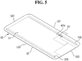
- the bracket 50 may include a connect hole 53, through which a display connector 35 (see FIG. 4 ) passes, near the first long edge (first long side LS1).
- the connect hole 53 may penetrate the bottom portion 51 of the bracket 50 in the thickness direction and may have, for example, a slit shape.
- the first force sensor 100 may have a recess NTH near the connect hole 53 of the bracket 50.
- the recess NTH may have the shape of a notch, and thus may also be referred to herein as a notch-shaped recess NTH. This will be described in detail with reference to FIGs. 4 and 5 .
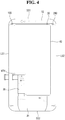
- FIG. 4 is a bottom view of the display device 1 according to an exemplary embodiment.
- FIG. 4 illustrates the bottom shape of the display device 1 excluding the bracket 50.
- the display device 1 is turned upside down. Thus, the left and right sides are reversed, and the positions of the first long side LS1 and the second long side LS2 are also reversed.
- FIG. 5 is a perspective view illustrating the arrangement of the bracket 50 and the force sensors 100 and 200 according to an exemplary embodiment.
- the display flexible circuit board 31 is connected to the display connector 35.
- the display flexible circuit board 31 is housed in the bracket 50, and the display connector 35 comes out of the bracket 50 through the connect hole 53 so as to be connected to an external terminal.
- the first force sensor 100 overlaps or physically contacts a space through which the display connector 35 comes out, there is a possibility that the first force sensor 100 will malfunction. Therefore, in exemplary embodiments, the first force sensor 100 includes the recess NTH at a corresponding position to avoid interfering with the display connector 35. Since the first force sensor 100 is recessed outward due to the recess NTH, in exemplary embodiments, the first force sensor 100 does not overlap or physically contact the display connector 35 passing through the connect hole 53.
- the recess NTH of the first force sensor 100 disposed in the bracket 50 may bypass the connect hole 53 in an outward direction.
- the display connector 35 may be made of, for example, a flexible circuit board. Although the display flexible circuit board 31 and the display connector 35 are formed as separate members and connected to each other in the drawings, the display flexible circuit board 31 itself may also pass through the connect hole 53 in exemplary embodiments.
- the second force sensor 200 may not include a notch-shaped recess.
- the first force sensor 100 includes the notch-shaped recess NTH, and the second force sensor 200 does not include the notch-shaped recess NTH.
- the force sensors 100 and 200 will now be described in more detail.
- FIG. 6 is an exploded perspective view of the first force sensor 100 according to an exemplary embodiment.
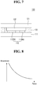
- FIG. 7 is a cross-sectional view taken along line VII-VII' of FIG. 6 .
- FIG. 8 is a graph illustrating the relationship between the electrical resistance of a force sensing layer 122 and a force.
- the structure and operation of the first force sensor 100 are described as an example.
- the second force sensor 200 has substantially the same structure and operation as the first force sensor 100, except for the presence of the recess NTH. Accordingly, for convenience of explanation, a duplicate description of the structure and operation of the second force sensor 200 will be omitted herein.
- the first force sensor 100 extends in one direction in a plane.
- a length of the first force sensor 100 in the extending direction is greater than a width of the first force sensor 100.
- the width of the first force sensor 100 may be between about 2 mm and about 6 mm.
- the length of the first force sensor 100 may be substantially similar to the lengths of the long sides LS1 and LS2 of the display device 1.
- the length of the first force sensor 100 may be, but embodiments are not limited to, about 80% to about 98% of the lengths of the long sides LS1 and LS2 of the display device 1.
- the length of the first force sensor 100 may be in the range of about 50 mm to about 300 mm or in the range of about 100 mm to about 150 mm.
- the first force sensor 100 includes a first substrate 110 and a second substrate 120 facing each other.
- the first substrate 110 includes a first base 111 and an electrode layer 112.
- the second substrate 120 includes a second base 121 and the force sensing layer 122.
- the first substrate 110 and the second substrate 120 are bonded together by a bonding layer 130.
- the first substrate 110 and the second substrate 120 may be, but embodiments are not limited to, films.
- Each of the first base 111 and the second base 121 may include, for example, polyethylene, polyimide, polycarbonate, polysulfone, polyacrylate, polystyrene, polyvinyl chloride, polyvinyl alcohol, polynorbornene, or polyester.
- each of the first base 111 and the second base 121 may be made of, for example, a polyethylene terephthalate (PET) film or a polyimide film.
- the electrode layer 112 is disposed on a surface of the first base 111.
- the surface of the first base 111 is a surface facing the second base 121.
- a thickness of the electrode layer 112 may be between about 2 um and about 8 um.
- the thickness of the electrode layer 112 may be about 4 um in an exemplary embodiment.
- the electrode layer 112 includes a first electrode 112TX and a second electrode 112RX.
- the first electrode 112TX may be, for example, a driving electrode
- the second electrode 112RX may be, for example, a sensing electrode.
- the first electrode 112TX and the second electrode 112RX may be disposed adjacent to each other, but are spaced apart from each other so as not to short-circuit.
- the first electrode 112TX and the second electrode 112RX may be disposed adjacent to each other (e.g., directly adjacent to each other with no other components disposed therebetween) without contacting each other.
- the first electrode 112TX and the second electrode 112RX may be disposed on the same layer.
- the first electrode 112TX and the second electrode 112RX may be made of the same material.
- the first electrode 112TX and the second electrode 112RX may include a conductive material such as silver (Ag) or copper (Cu).
- the first electrode 112TX and the second electrode 112RX may be formed, for example, by a screen printing method.
- the first electrode 112TX may be formed as a single piece along the direction in which the first force sensor 100 extends
- the second electrode 112RX, which is separated from the first electrode 112TX may be formed as a single piece along the direction in which the first force sensor 100 extends.
- the force sensing layer 122 is disposed on a surface of the second base 121.
- the surface of the second base 121 is a surface facing the first base 111.
- the force sensing layer 122 may include a force sensitive material.
- the force sensitive material may include metal nanoparticles such as, for example, nickel, aluminum, tin or copper, or may include carbon.
- the force sensitive material may be provided in a polymer resin in the form of, but embodiments are not limited to, particles.
- the electrical resistance of the force sensing layer 122 decreases as the force increases. By using this characteristic, it is possible to sense whether the force has been applied, as well as the magnitude of the force.
- a surface of the force sensing layer 122 is in contact with or at least adjacent to surfaces of the first electrode 112TX and the second electrode 112RX.
- the surface of the force sensing layer 122 is brought into contact with the surfaces of the first electrode 112TX and the second electrode 112RX at a corresponding portion. Therefore, the first electrode 112TX and the second electrode 112RX may be physically connected by the force sensing layer 122.
- the force sensing layer 122 lying between the first electrode 112TX and the second electrode 112RX may act as an electrical resistor.
- the force sensing layer 122 When no force or little force is applied to the force sensing layer 122, the force sensing layer 122 has a high resistance. In this case, even if a driving voltage is applied to the first electrode 112TX, a current hardly flows to the second electrode 112RX. On the other hand, when a large force is applied to the force sensing layer 122, the resistance of the force sensing layer 122 is reduced, thus increasing the amount of current flowing between the first electrode 112TX and the second electrode 112RX.
- the thickness of the force sensing layer 122 may be, but embodiments are not limited to, a thickness that is thicker than the electrode layer 112.
- the thickness of the force sensing layer 122 may be between about 4 um and about 12 um.
- the thickness of the force sensing layer 122 may be about 8 um.
- the first force sensor 100 may further include the bonding layer 130 disposed between the first base 111 and the second base 121.
- the bonding layer 130 bonds the first base 111 and the second base 121.
- the bonding layer 130 may be disposed along the periphery of the first base 111 and the second base 121.
- the bonding layer 130 may completely surround the periphery of the first base 111 and the second base 121, thus, sealing the first force sensor 100. That is, the bonding layer 130 may serve as a gasket. Further, the bonding layer 130 may also serve as a spacer that maintains a constant gap between the first base 111 and the second base 121.
- the bonding layer 130 does not overlap the electrode layer 112 and the force sensing layer 122.
- a thickness of the bonding layer 130 may be in the range of about 5 um to about 50 um, or in the range of about 12 um to about 30 um.
- the bonding layer 130 may be made of a force-sensitive adhesive layer or an adhesive layer.
- the bonding layer 130 may first be attached to one of the surface of the first base 111 and the surface of the second base 121, and then attached to the surface of the other base 111 or 121 in the process of assembling the first base 111 and the second base 121.
- a bonding layer may be provided on each of the surface of the first base 111 and the surface of the second base 121, and then the bonding layer of the first base 111 and the bonding layer of the second base 121 may be bonded together in the process of assembling the first base 111 and the second base 121.
- the first force sensor 100 may be placed in the display device 1 such that the first base 111 having the electrode layer 112 faces the display panel 30. That is, the other surface (outer surface) of the first base 111 may be attached to the lower surface of the display panel 30, and the other surface (outer surface) of the second base 121 may be attached to the bracket 50.
- exemplary embodiments are not limited to this case.
- the arrangement directions of the first base 111 and the second base 121 in the display device 1 may also be opposite to the directions described above.
- FIG. 9 is a layout view of the first force sensor 100 and the second force sensor 200 according to an exemplary embodiment.
- the arrangement of the first substrate 110 and the second substrate 120 of the first force sensor 100 is illustrated on the left side of FIG. 9
- the arrangement of a first substrate 210 and a second substrate 220 of the second force sensor 200 is illustrated on the right side of FIG. 9 .
- each of the first force sensor 100 and the second force sensor 200 includes a plurality of sensing regions SR1 and SR2.
- the sensing regions SR1 and SR2 are regions capable of sensing forces.
- the sensing regions SR1 and SR2 may sense forces at their corresponding positions independently of each other.
- the second force sensor includes an electrode layer 212.
- the sensing regions SR1 and SR2 may be arranged in a longitudinal direction of each of the first force sensor 100 and the second force sensor 200. In an exemplary embodiment, the sensing regions SR1 and SR2 may be arranged in one row. Neighboring sensing regions SR1 and SR2 may be arranged continuously. Alternatively, the neighboring sensing regions SR1 and SR2 may be spaced apart from each other. That is, a non-sensing region NSR may be disposed between the sensing regions SR1 and SR2.
- the first force sensor 100 is disposed adjacent to a first edge of the display panel 30 and extends along the first edge.
- the first force sensor 100 includes a plurality of first sensing regions SR1 disposed between a first end of the first force sensor 100 and a second end of the first force sensor 100.
- the second sensing region SR2 is disposed closer to the second end of the first force sensor 100 than the first sensing regions SR1, and has a wider area than each of the first sensing regions SR1.
- the second force sensor 200 is disposed adjacent to a second edge of the display panel 30.
- the second edge faces the first edge, and the second force sensor 200 extends along the second edge.
- the second force sensor 200 includes a plurality of first sensing regions SR1 disposed between a first end of the second force sensor 200 and a second end of the second force sensor 200, and a second sensing region SR2 disposed closer to the second end of the second force sensor 200 than the first sensing regions SR1 included in the second force sensor 200.
- the second sensing region SR2 included in the second force sensor 200 has a wider area than each of the first sensing regions SR1 included in the second force sensor 200.
- the first force sensor 100 includes the recess NTH disposed at an inner side of the first force sensor 100.
- the first force sensor 100 includes a plurality of first sensing regions SR1 disposed on a first side of the recess NTH and a second sensing region SR2 disposed on a second side of the recess NTH.
- the second sensing region SR2 disposed on the second side of the recess NTH has a wider area than each of the first sensing regions SR1 disposed on the first side of the recess NTH.
- the first electrode 112TX of the first force sensor 100 or a first electrode of the second force sensor 200, the second electrode 112RX of the first force sensor 100 or a second electrode of the second force sensor 200, and the force sensing layer 122 or 222, are disposed in each of the sensing regions SR1 and SR2.
- the second electrode 112RX of the first force sensor 100 or the second electrode of the second force sensor 200 serve as a sensing electrode that is a separate cell electrode disposed in each of the sensing regions SR1 and SR2, and the first electrode 112TX of the first force sensor 100 or the first electrode of the second force sensor 200 serve as a driving electrode and is a common electrode, all portions of which are electrically connected regardless of the sensing regions SR1 and SR2.
- the force sensing layer 122 or 222 may also be patterned and disposed as a separate layer in each of the sensing regions SR1 and SR2.
- the sensing regions SR1 and SR2 may have different areas depending on their use.
- the area of a second sensing region SR2 e.g., a squeezing sensing region
- the second sensing region SR2 has the same width as the first sensing region SR1, but may have a greater length (width in the extending direction of a force sensor) than the first sensing region SR1.
- the length of the second sensing region SR2 may be about three to about fifteen times the length of the first sensing region SR1.
- the length of the first sensing region SR1 may be between about 4 mm and about 5 mm
- the length of the second sensing region SR2 may be between about 30 mm and about 60 mm.
- a plurality of first sensing regions SR1 may be arranged in a direction from an upper end toward a lower end of each of the first force sensor 100 and the second force sensor 200, and one second sensing region SR2 may be disposed near the lower end of each of the first force sensor 100 and the second force sensor 200.
- the positions of the first sensing regions SR1 and the second sensing region SR2 in the first force sensor 100 may be distinguished based on the recess NTH.
- the first sensing regions SR1 may be disposed above the recess NTH
- the second sensing region SR2 may be disposed below the recess NTH.
- the recess NTH may separate the first sensing regions SR1 from the second sensing region SR2.
- the number of the first sensing regions SR1 disposed above the recess NTH may be selected from, but embodiments are not limited to, the range of 2 to 20 or the range of 5 to 15.
- the second force sensor 200 may have the first sensing regions SR1 and the second sensing region SR2 at positions corresponding to the first sensing regions SR1 and the second sensing region SR2 of the first force sensor 100.
- the sensing regions SR1 and SR2 of the first force sensor 100 and the sensing regions SR1 and SR2 of the second force sensor 200 may be substantially symmetrical to each other in terms of number, area, gap, position, etc. However, exemplary embodiments are not limited thereto.
- the recess NTH of the first force sensor 100 may be located in the middle or below the middle of the first force sensor 100 in the longitudinal direction of the first force sensor 100, as illustrated in FIG. 9 .
- a distance from the lower end of the first force sensor 100 to the recess NTH in a plan view may be about 30% to about 50% of the total length of the first force sensor 100.
- the distance from the lower end of the first force sensor 100 to the recess NTH may be between about 50 mm and about 60 mm.
- the recess NTH is formed at the inner side of the first force sensor 100.
- a width of the recess NTH recessed inward from the inner side of the first force sensor 100 may be between about 1 mm and about 4 mm.
- a width of the recess NTH recessed inward from the inner side of the first force sensor 100 may be about 2 mm.
- a length of the recess NTH may be about equal to the width of the recess NTH.
- the length of the recess NTH may be about equal to or greater than that of the connect hole 53.
- a recessed region of the recess NTH may overlap the connect hole 53.
- the recessed shape of the recess NTH may be, for example, a rectangular shape or a square shape.
- the recessed shape of the recess NTH is not limited to the rectangular shape or the square shape in embodiments.
- the recessed shape of the recess NTH may include a concave curve.
- the first electrode 112TX of the first force sensor 100 or the first electrode of the second force sensor 200, and the second electrode 112RX of the first force sensor 100 or the second electrode of the second force sensor 200 may be, for example, comb-shaped electrodes.
- the first electrode 112TX of the first force sensor 100 or the first electrode of the second force sensor 200, and the second electrode 112RX of the first force sensor 100 or the second electrode of the second force sensor 200 may be arranged such that the comb shapes are engaged with each other.
- the first electrode 112TX of the first force sensor 100 or the first electrode of the second force sensor 200, and the second electrode 112RX of the first force sensor 100 or the second electrode of the second force sensor 200 may each include a stem electrode (or a connection electrode) and branch electrodes (or finger electrodes).
- the first electrode 112TX of the first force sensor 100 or the first electrode of the second force sensor 200, and the second electrode 112RX of the first force sensor 100 or the second electrode of the second force sensor 200 may be arranged such that the branch electrodes are alternately disposed.
- This arrangement increases an area in which the first electrode 112TX of the first force sensor 100 or the first electrode of the second force sensor 200, and the second electrode 112RX of the first force sensor 100 or the second electrode of the second force sensor 200 face each other, thereby enabling effective force sensing.
- the first electrode 112TX of the first force sensor 100 is structured to include a first stem electrode 112TX_ST extending in the longitudinal direction, and a plurality of first branch electrodes 112TX_BR branching in the width direction from the first stem electrode 112TX_ST.
- the first electrode of the second force sensor 200 is structured to include a first stem electrode 212TX_ST extending in the longitudinal direction, and a plurality of first branch electrodes 212TX_BR branching in the width direction from the first stem electrode 212TX_ST.
- the first stem electrode 112TX_ST or 212TX_ST is disposed over the sensing regions SR1 and SR2 to provide a voltage (a driving voltage) to the sensing regions SR1 and SR2.
- the first stem electrode 112TX_ST or 212TX_ST extends up to the non-sensing region NSR between neighboring sensing regions SR1 and SR2, and electrically connects portions of the first stem electrode 112TX_ST or 212TX_ST which are disposed in the neighboring regions SR1 and SR2.
- the first stem electrode 112TX_ST of the first force sensor 100 may be disposed adjacent to the outer side of the first force sensor 100 which is opposite the inner side where the recess NTH is formed.
- exemplary embodiments are not limited to this case.
- the first stem electrode 112TX_ST of the first force sensor 100 may also be disposed on the inner side of the first force sensor 100 where the recess NTH is formed.
- the first stem electrode 112TX_ST of the first force sensor 100 may be bent several times along the shape of the recess NTH of the first force sensor 100 to bypass the recess NTH, and then extend to the lower end of the first force sensor 100, as illustrated in FIG. 15 .
- the first stem electrode 212TX_ST of the second force sensor 200 may be disposed adjacent to an outer side of the second force sensor 200 as illustrated in FIG. 9 .
- exemplary embodiments are not limited thereto.
- the first stem electrode 212TX_ST of the second force sensor 200 may be disposed adjacent to an inner side of the second force sensor 200. Since the second force sensor 200 does not include the recess NTH, it may extend straight without being bent to bypass the recess NTH, on whichever side the second force sensor 200 is disposed.
- the first branch electrodes 112TX_BR or 212TX_BR branch from the first stem electrode 112TX_ST or 212TX_ST and extend in the width direction.
- the first branch electrodes 112TX_BR or 212TX_BR may be disposed in the sensing regions SR1 and SR2 and are not disposed in the non-sensing region NSR.
- the first branch electrodes 112TX_BR is not disposed in the region.
- the first branch electrodes 212TX_BR are not disposed in a region corresponding to the recess NTH.
- neighboring first branch electrodes 112TX_BR or 212TX_BR may be spaced apart from each other by a predetermined distance, and a second branch electrode 112RX_BR or 212RX BR of the second electrode 112RX of the first force sensor 100 or the second electrode of the second force sensor 200 may be disposed in each space between the neighboring first branch electrodes 112TX_BR or 212TX_BR.
- the number of the first branch electrodes 112TX_BR or 212TX_BR disposed in one sensing region SR1 or SR2 may vary depending on the area of the sensing region SR1 or SR2.
- the number of the first branch electrodes 112TX_BR or 212TX_BR disposed in one sensing region SR1 or SR2 may be between about 2 and about 20 based on each first sensing region SR1.
- the first branch electrodes 112TX_BR or 212TX_BR disposed in the second sensing region SR2 may have the same width and spacing as the first branch electrodes 112TX_BR or 212TX_BR disposed in each first sensing region SR1.
- the number of the first branch electrodes 112TX_BR or 212TX_BR disposed in the second sensing region SR2 may be greater in proportion to the area of the second sensing region SR2.
- the second electrode 112RX of the first force sensor 100 or the second electrode of the second force sensor 200 includes a second stem electrode 112RX_ST or 212RX_ST extending in the longitudinal direction, and a plurality of second branch electrodes 112RX_BR or 212RX_BR branching from the second stem electrode 112RX_ST or 212RX_ST.
- the second stem electrode 112RX_ST or 212RX_ST faces the first stem electrode 112TX_ST or 212TX_ST.
- the second stem electrode 112RX_ST or 212RX_ST may be disposed adjacent to the outer side of each of the force sensors 100 and 200.
- the second stem electrode 112RX_ST or 212RX_ST covers one sensing region SR1 or SR2.
- the second stem electrode 112RX_ST or 212RX_ST is disposed in each of the sensing regions SR1 and SR2, and the second stem electrodes 112RX_ST or 212RX_ST disposed in different sensing regions SR1 and SR2 are electrically insulated from each other.
- Each second stem electrode 112RX_ST or 212RX_ST is connected to an independent sensing wiring 112RX_WR or 212RX_WR.
- Each sensing wiring 112RX_WR or 212RX_WR may extend in one direction and may be connected to a controller. Accordingly, each sensing wiring 112RX_WR or 212RX_WR may transmit data about the voltage or the amount of current applied to a corresponding second electrode 112RX or 212RX to the controller.
- the second branch electrodes 112RX_BR or 212RX_BR branch from the second stem electrode 112RX_ST or 212RX_ST and extend in the width direction.
- the extending direction of the second branch electrodes 112RX_BR or 212RX_BR and the extending direction of the first branch electrodes 112TX_BR or 212TX_BR are opposite to each other.
- the second branch electrodes 112RX_BR or 212RX_BR are disposed between the first branch electrodes 112TX_BR or 212TX_BR.
- the number of the first branch electrodes 112TX_BR or 212TX_BR and the number of the second branch electrodes 112RX_BR or 212RX_BR in one sensing region SR1 or SR2 may be equal, however, exemplary embodiments are not limited thereto.
- the first branch electrodes 112TX_BR or 212TX_BR and the second branch electrodes 112RX_BR or 212RX_BR may be alternately arranged.
- a gap between neighboring first and second branch electrodes 112TX_BR and 112RX_BR or 212TX_BR and 212RX_BR in one sensing region SR1 or SR2 may be uniform, however, exemplary embodiments are not limited thereto.
- a gap between nearest branch electrodes 112TX_BR and 112RX_BR or 212TX_BR and 212RX_BR in different sensing regions SR1 and SR2, which neighbor each other with the non-sensing region NSR interposed between them, may be greater than the gap between the branch electrodes 112TX_BR and 112RX_BR or 212TX_BR and 212RX_BR in one sensing region SR1 or SR2.
- the second electrode 112RX of the first force sensor 100 and the second electrode of the second force sensor 200 are not disposed in the recess NTH of the first force sensor 100 and in a region of the second force sensor 200 which corresponds to the recess NTH. In some cases, however, the sensing wirings 112RX_WR and 212RX_WR of the second electrode 112RX of the first force sensor 100 and the second electrode of the second force sensor 200 may pass through the above regions.
- the force sensing layer 122 or 222 may have a shape corresponding to each of the sensing regions SR1 and SR2.
- the force sensing layer 122 or 222 covers each of the sensing regions SR1 and SR2.
- the first branch electrodes 112TX_BR or 212TX_BR and the second branch electrodes 112RX_BR or 212RX_BR in each of the sensing regions SR1 and SR2 may overlap the force sensing layer 122 or 222 in the thickness direction.
- the force sensors 100 and 200 described above can be used as input devices for various electronic devices including the display device 1, such as, for example, a smartphone and a tablet PC.
- the force sensors 100 and 200 can be used in place of physical input buttons or in combination with physical input buttons.
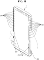
- FIGs. 10 and 11 are diagrams illustrating a method of transmitting a force signal to the display device 1 according to an exemplary embodiment.
- the display device 1 is implemented in a smartphone.
- the force sensors 100 and 200 are disposed on the long sides in place of physical input buttons.
- a smartphone including the display device 1 may be implemented without any physical buttons.
- a pressing recognition region is a region configured to sense a press input operation provided by the user. That is, in FIG. 10 , a user is pressing a specific position with an index finger while gripping the display device 1 with fingers. At the specific position, a first sensing region SR1 of the force sensor 100 or 200 is disposed.
- the resistance of the force sensing layer 122 or 222 is changed, and the change in the resistance of the force sensing layer 122 or 222 is sensed through the second electrode 112RX of the first force sensor 100 or the second electrode of the second force sensor 200 to identify whether the force has been applied to the specific position, as well as the magnitude of the force.
- a preprogrammed operation of the display device 1 may be output according to the force and/or the magnitude of the force applied to the specific position. For example, a preprogrammed function such as screen adjustment, screen lock, screen conversion, application calling, application execution, picture taking, or telephone reception may be performed. Different operations may be preprogrammed for different first sensing regions SR1. Therefore, as the number of the first sensing regions SR1 increases, the display device 1 can produce additional outputs.
- a squeezing recognition region is a region configured to sense a squeezing input operation provided by the user. That is, in FIG. 11 , the user is squeezing a relatively large area using the palm and fingers while gripping the display device 1 with the fingers.
- the second sensing region SR2 is disposed in the area in which the squeezing is performed to sense whether a force has been applied by the squeezing, as well as the magnitude of the force.
- a preprogrammed operation of the display device 1 may be performed according to the sensing result (e.g., when it is sensed that the second sensing region SR2 has been squeezed).
- the user may perform the squeezing operation by naturally applying force using the entire hand while gripping the display device 1. Since the user can quickly perform the squeezing operation without the elaborate movement of the hand while gripping the display device 1, a simpler and quicker input is possible. For example, the user may provide a squeeze input without being concerned with the precise location at which each of the fingers are located on the display device 1. Therefore, the second sensing region SR2 can be used as an input medium for a frequently used function or a program requiring rapid inputs, such as using a camera application to take pictures.
- FIG. 12 is a layout view of a first force sensor 100 and a second force sensor 200_1 according to an exemplary embodiment.
- the exemplary embodiment of FIG. 12 is different from the exemplary embodiment of FIG. 9 in that a second sensing region SR2 of the second force sensor 200_1 has a wider area than a second sensing region SR2 of the first force sensor 100.
- the second sensing region SR2 of the second force sensor 200_1 extends further toward an upper end than the second sensing region SR2 of the first force sensor 100.
- the second sensing region SR2 of the second force sensor 200_1 may extend up to a region corresponding to a recess NTH of the first force sensor 100.
- the areas in which the palm or the fingers naturally touch the first long side and the second long side may be different.
- the exemplary embodiment of FIG. 12 enables a more precise force measurement in this case.
- reference numeral 210_1 indicates a first substrate of the second force sensor 200_1
- reference numeral 220_1 indicates a second substrate of the second force sensor 200_1.
- FIG. 13 is a layout view of a first force sensor 100_2 and a second force sensor 200_2 according to an exemplary embodiment.
- FIG. 13 a case in which a force sensing layer 122 or 222 is formed as a single piece without being divided into segments respectively corresponding to sensing regions SR1 and SR2 is illustrated.
- a second substrate 120_2 or 220_2 of each of the first force sensor 100_2 and the second force sensor 200_2 includes the force sensing layer 122 or 222 formed as a single piece.
- the force sensing layer 122 or 222 is formed as a single piece, the second electrode 112RX of the first force sensor 100_2 or the second electrode of the second force sensor 200_2, or the first electrode 112TX of the first force sensor 100_2 or the first electrode of the second force sensor 200_2, is still a functionally separate electrode disposed in each of the sensing regions SR1 and SR2. Therefore, when a force is applied to a specific sensing region SR1 or SR2, the transmission of a sensing signal to other sensing regions SR1 and SR2 can be prevented, thereby preventing the generation of noise at an input position.
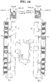
- FIG. 14 is a layout view of a first force sensor 100_3 and a second force sensor 200_3 according to an exemplary embodiment.
- a non-sensing region NSR is disposed in portions of a second sensing region SR2 of each of the first force sensor 100_3 and the second force sensor 200_3 is illustrated.
- first branch electrodes 112TX_BR or 212TX_BR and second branch electrodes 112RX_BR or 212RX_BR of a first substrate 110_3 or 210_3 may be arranged similarly to a plurality of first sensing regions SR1. That is, the first branch electrodes 112TX_BR or 212TX_BR and the second branch electrodes 112RX_BR or 212RX_BR are alternately arranged in predetermined numbers at a first interval in the longitudinal direction, are not arranged by a second interval larger than the first interval, and then are alternately arranged again at the first interval.
- the second branch electrodes 112RX_BR or 212RX_BR in the second sensing region SR2 are electrically connected by one second stem electrode 112RX_ST or 212RX_ST.
- a force sensing layer 122 or 222 of a second substrate 120_3 or 220_3 may also be patterned like the first sensing regions SR1.
- exemplary embodiments are not limited to this case, and the force sensing layer 122 or 222 in the second sensing region SR2 may also be formed as a single piece as illustrated in FIG. 9 without being patterned.
- the first and second electrodes 112TX and 112RX of the first force sensor 100_3, or the first and second electrodes of the second force sensor 200_3, and the force sensing layer 122 or 222 have similar patterns in the first sensing regions SR1 as well as in the second sensing region SR2. Therefore, problems that may occur due to differences in shape can be prevented.
- the non-sensing region NSR is disposed in portions of the second sensing region SR2, since the entire second sensing region SR2 is sensed using one second electrode (e.g., the second electrode 112RX of the first force sensor 100_3 or the second electrode of the second force sensor 200_3) as in the exemplary embodiment of FIG. 9 and a squeezing operation is performed on a wide area, a squeezing input may be accurately recognized.
- FIG. 15 is a layout view of a first force sensor 100_4 and a second force sensor 200_4 according to an exemplary embodiment.
- the exemplary embodiment of FIG. 15 is different from the exemplary embodiment of FIG. 9 in that a second electrode 112RX of the first force sensor 100_4 or a second electrode of the second force sensor 200_4 is formed as a single piece.
- all portions of the second electrode 112RX of the first force sensor 100_4 or the second electrode of the second force sensor 200_4 are connected by a second stem electrode 112RX_ST or 212RX_ST, like a first electrode 112TX of the first force sensor 100_4 or a first electrode of the second force sensor 200_4. Therefore, when a force is applied, it is possible to measure the presence or absence of the force and the magnitude of the force, but it may be difficult to identify a position at which the force has been applied.
- the first force sensor 100_4 includes a first substrate 110_4 and a second substrate 120_4, and the second force sensor 200_4 includes a first substrate 210_4 and a second substrate 220_4.
- the position at which the force has been applied may be identified through a touch member 20 (see FIG. 2 ). That is, a touch electrode may be disposed in regions of the touch member 20 which overlap the force sensors 100_4 and 200_4. The touch electrode may be used to detect the presence or absence of a touch and the position of the touch. The presence or absence of a force and the magnitude of the force may be measured by the force sensors 100_4 and 200_4 and used as an input signal.
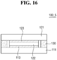
- FIG. 16 is a cross-sectional view of a first force sensor 100_5 according to an exemplary embodiment.
- FIG. 17 is a layout view of the first force sensor 100_5 of FIG. 16 . Referring to FIGs. 16 and 17 , the shape and arrangement of first and second electrodes 113 and 123 of the first force sensor 100_5 according to the current exemplary embodiment are different from those of the exemplary embodiment of FIG. 9 .
- a first substrate 110_5 includes a first base 111 and the first electrode 113 disposed on the first base 111.
- a second substrate 120_5 includes a second base 121, the second electrode 123 disposed on the second base 121, and a force sensing layer 122 disposed on the second electrode 123.
- the first electrode 113 faces the force sensing layer 122 and is in contact with or adjacent to the force sensing layer 122.
- the first electrode 113 and the second electrode 123 face each other in the thickness direction with the force sensing layer 122 interposed between them.
- the resistance of the input sensing layer 122 is changed, thereby changing the amount of current flowing between the first electrode 113 and the second electrode 123.
- the force input can be sensed.
- the first electrode 113 is a separate sensing electrode disposed in each sensing region, and the second electrode 123 is a driving electrode formed as a whole-plate electrode.
- the first electrode 113 may also be formed as a whole-plate electrode, and the second electrode 123 may also be formed as a sensing electrode.
- a second force sensor may also have the same configuration as the first force sensor 100_5 except for the inclusion of a recess NTH.
- FIG. 18 is a cross-sectional view of a display device 2 according to an exemplary embodiment.
- FIG. 18 shows that the attachment position of a first force sensor 100 and a second force sensor 200 in the display device 2 can be changed. That is, as illustrated in FIG. 18 , the first force sensor 100 and the second force sensor 200 can be directly attached to a window 10 without overlapping a display panel 30 and a touch member 20.
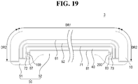
- FIG. 19 is a cross-sectional view of a display device 3 according to an exemplary embodiment.
- FIG. 19 shows that a second area DR2 of the display device 3 can lie in a plane located at an angle of about 90 degrees or more to a first area DR1.
- the second area DR2 may substantially form side surfaces of the display device 3.
- the second area DR2 may be a display surface, and may correspond to a non-display area.
- a first force sensor 100 and a second force sensor 200 are attached to the second area DR2 of the display device 3. Since the first force sensor 100 and the second force sensor 200 are attached to the side surfaces of the display device 3 in the exemplary embodiment of FIG. 19 , a user can easily input a force while gripping the display device 3.
- embodiments can provide a display device, comprising: a display panel; and a first force sensor disposed adjacent to a first edge of the display panel, wherein the first force sensor extends along the first edge, wherein the first force sensor comprises a plurality of first sensing regions and a second sensing region, the first sensing regions disposed closer to a first end of the first force sensor than the second sensing region, and the second sensing region disposed closer to a second end of the first force sensor than the first sensing regions, wherein the second sensing region has a larger area than each of the first sensing regions.
- the first force sensor may comprise a first electrode and a second electrode separated from the first electrode, wherein the first electrode may be disposed over the first sensing regions and the second sensing region, and the second electrode may be disposed separately in each of the first and second sensing regions.
- the first force sensor may further comprise a force sensing layer comprising a force sensitive material having a resistance that varies according to a force, wherein the first electrode and the second electrode contact the force sensing layer.
- the first and second sensing regions may be arranged in a longitudinal direction of the first force sensor.
- the first and second sensing regions are arranged in a row or a column. Neighboring first and second sensing regions may be arranged continuously. Alternatively, the neighboring first and second sensing regions may be spaced apart from each other. That is, a non-sensing region may be disposed between the first and second sensing regions.
- Each first sensing region of the first force sensor may be a pressing recognition region, and the second sensing region of the first force sensor may be a squeezing recognition region.
- a recess is disposed at an inner side of the first force sensor, wherein the first sensing region is disposed on a first side of the recess and the second sensing region is disposed on a second side of the recess.
- the recess may be notch-shaped.
- a bracket may be provided which houses the display panel and the first force sensor, the bracket comprising a connect hole through which a connector passes, wherein the recess bypasses the connect hole in an outward direction.
- the display device further comprises a second force sensor disposed adjacent to a second edge of the display panel, wherein the second edge faces the first edge and the second force sensor extends along the second edge, wherein the second force sensor comprises a plurality of third sensing regions and a fourth sensing region, the third sensing regions disposed closer to a first end of the second force sensor than the fourth sensing region, and the second sensing region disposed closer to a second end of the second force sensor than the third sensing regions, wherein the fourth sensing region has a larger area than each of the third sensing regions.
- the first sensing regions and the third sensing regions may be pressing recognition regions, and the second sensing region and the fourth sensing region may be squeezing recognition regions.
- Embodiments can also provide a display device comprising: a display panel; and a first force sensor disposed adjacent to a first edge of the display panel, wherein the first force sensor extends along the first edge and comprises a recess disposed at an inner side of the first force sensor, wherein the first force sensor comprises a plurality of first sensing regions a second sensing region, wherein the recess is disposed between the first sensing regions and the second sensing region, and wherein the second sensing region has a larger area than each of the first sensing regions.
- the recess may be notch-shaped.
- a second force sensor may be disposed adjacent to a second edge of the display panel that faces the first edge of the display panel, and in some embodiments, the second force sensor does not comprise the recess disposed in the first force sensor or any other recess.
- Embodiments can also provide a force sensor, comprising: a recess disposed at one side of the force sensor; a plurality of first sensing regions that sense a first force; and a second sensing region that senses a second force, wherein the recess is disposed between the first sensing regions and the second sensing region, wherein the second sensing region has a larger area than each of the first sensing regions.
- a force sensor and a display device can prevent a malfunction due to interference between components, and can simplify an input method.
Landscapes
- Engineering & Computer Science (AREA)
- Theoretical Computer Science (AREA)
- General Engineering & Computer Science (AREA)
- Physics & Mathematics (AREA)
- General Physics & Mathematics (AREA)
- Human Computer Interaction (AREA)
- Computer Hardware Design (AREA)
- Devices For Indicating Variable Information By Combining Individual Elements (AREA)
- Force Measurement Appropriate To Specific Purposes (AREA)
Applications Claiming Priority (1)
| Application Number | Priority Date | Filing Date | Title |
|---|---|---|---|
| KR1020180056273A KR102473627B1 (ko) | 2018-05-17 | 2018-05-17 | 압력 센서 및 이를 포함하는 표시 장치 |
Publications (3)
| Publication Number | Publication Date |
|---|---|
| EP3579089A2 true EP3579089A2 (de) | 2019-12-11 |
| EP3579089A3 EP3579089A3 (de) | 2020-04-08 |
| EP3579089B1 EP3579089B1 (de) | 2023-11-29 |
Family
ID=66589375
Family Applications (1)
| Application Number | Title | Priority Date | Filing Date |
|---|---|---|---|
| EP19174990.2A Active EP3579089B1 (de) | 2018-05-17 | 2019-05-16 | Kraftsensor und anzeigevorrichtung damit |
Country Status (4)
| Country | Link |
|---|---|
| US (1) | US12066340B2 (de) |
| EP (1) | EP3579089B1 (de) |
| KR (1) | KR102473627B1 (de) |
| CN (1) | CN110502139B (de) |
Cited By (1)
| Publication number | Priority date | Publication date | Assignee | Title |
|---|---|---|---|---|
| US10719160B2 (en) | 2018-07-31 | 2020-07-21 | Samsung Display Co., Ltd. | Display device |
Families Citing this family (9)
| Publication number | Priority date | Publication date | Assignee | Title |
|---|---|---|---|---|
| KR102555824B1 (ko) * | 2018-07-31 | 2023-07-14 | 삼성디스플레이 주식회사 | 표시 장치 |
| KR102636883B1 (ko) | 2018-08-17 | 2024-02-15 | 삼성디스플레이 주식회사 | 표시 장치 |
| KR102636887B1 (ko) | 2018-08-17 | 2024-02-15 | 삼성디스플레이 주식회사 | 표시 장치 |
| KR102582316B1 (ko) * | 2018-08-20 | 2023-09-25 | 삼성디스플레이 주식회사 | 표시 장치 |
| CN112860008A (zh) * | 2019-11-28 | 2021-05-28 | 北京小米移动软件有限公司 | 显示屏模组、终端设备及指纹识别方法 |
| KR102814906B1 (ko) * | 2019-12-19 | 2025-06-02 | 삼성디스플레이 주식회사 | 표시 장치 |
| US20210257582A1 (en) * | 2020-02-14 | 2021-08-19 | Samsung Display Co., Ltd. | Display device |
| CN111508371A (zh) * | 2020-05-26 | 2020-08-07 | 武汉华星光电半导体显示技术有限公司 | 可折叠显示装置 |
| KR20230084389A (ko) * | 2021-12-03 | 2023-06-13 | 삼성디스플레이 주식회사 | 표시 장치 |
Family Cites Families (35)
| Publication number | Priority date | Publication date | Assignee | Title |
|---|---|---|---|---|
| US7800592B2 (en) | 2005-03-04 | 2010-09-21 | Apple Inc. | Hand held electronic device with multiple touch sensing devices |
| US7656393B2 (en) * | 2005-03-04 | 2010-02-02 | Apple Inc. | Electronic device having display and surrounding touch sensitive bezel for user interface and control |
| WO2005008444A2 (en) | 2003-07-14 | 2005-01-27 | Matt Pallakoff | System and method for a portbale multimedia client |
| US20050248548A1 (en) * | 2004-04-14 | 2005-11-10 | Masahiro Tsumura | Acoustic touch sensor |
| KR20050115346A (ko) | 2004-06-02 | 2005-12-07 | 삼성전자주식회사 | 표시 장치 및 그 구동 방법 |
| US7113179B2 (en) * | 2004-06-23 | 2006-09-26 | Interlink Electronics, Inc. | Force sensing resistor with calibration element and method of manufacturing same |
| JP4584210B2 (ja) | 2006-08-25 | 2010-11-17 | 京セラ株式会社 | 電子機器 |
| EP3654141A1 (de) | 2008-10-06 | 2020-05-20 | Samsung Electronics Co., Ltd. | Verfahren und vorrichtung zur anzeige einer graphischen benutzerschnittstelle in abhängigkeit vom kontaktmuster eines benutzers |
| US20100134424A1 (en) * | 2008-12-02 | 2010-06-03 | At&T Mobility Ii Llc | Edge hand and finger presence and motion sensor |
| US8654524B2 (en) | 2009-08-17 | 2014-02-18 | Apple Inc. | Housing as an I/O device |
| US8633916B2 (en) | 2009-12-10 | 2014-01-21 | Apple, Inc. | Touch pad with force sensors and actuator feedback |
| US9886116B2 (en) | 2012-07-26 | 2018-02-06 | Apple Inc. | Gesture and touch input detection through force sensing |
| US9035752B2 (en) * | 2013-03-11 | 2015-05-19 | Amazon Technologies, Inc. | Force sensing input device under an unbroken exterior portion of a device |
| US9904394B2 (en) | 2013-03-13 | 2018-02-27 | Immerson Corporation | Method and devices for displaying graphical user interfaces based on user contact |
| US9575557B2 (en) * | 2013-04-19 | 2017-02-21 | Qualcomm Incorporated | Grip force sensor array for one-handed and multimodal interaction on handheld devices and methods |
| KR102148789B1 (ko) * | 2013-09-20 | 2020-08-27 | 디아이씨 가부시끼가이샤 | 점착테이프 및 전자 기기 |
| WO2015123322A1 (en) * | 2014-02-12 | 2015-08-20 | Apple Inc. | Force determination employing sheet sensor and capacitive array |
| KR102205281B1 (ko) * | 2014-05-28 | 2021-01-20 | 엘지전자 주식회사 | 이동 단말기 |
| FR3021134B1 (fr) * | 2014-05-14 | 2023-01-06 | Lg Electronics Inc | Terminal mobile |
| KR20160013760A (ko) * | 2014-07-28 | 2016-02-05 | 삼성전자주식회사 | 터치 신호를 이용한 디바이스에 대한 압력 측정 방법 및 압력을 측정하는 디바이스 |
| US9664577B1 (en) * | 2014-08-26 | 2017-05-30 | Amazon Technologies, Inc. | Force-sensitive resistor assemblies and methods |
| JP2017537416A (ja) * | 2014-10-30 | 2017-12-14 | ティモシー ジン イン スートゥー | タッチを感知し、圧力を感知し、表示可能である側面を備えた電子デバイス |
| KR20160068439A (ko) * | 2014-12-05 | 2016-06-15 | 삼성전자주식회사 | 하이브리드 터치 기반 전자 장치 및 그 제어 방법 |
| KR20160149982A (ko) | 2015-06-18 | 2016-12-28 | 삼성전자주식회사 | 입력장치를 구비한 전자장치 |
| WO2017011810A1 (en) | 2015-07-15 | 2017-01-19 | Interlink Electronics, Inc. | Force sensing bezel touch interface |
| KR20170135602A (ko) | 2016-05-31 | 2017-12-08 | 엘지디스플레이 주식회사 | 터치 센서 및 터치 센서를 포함하는 유기발광 표시장치 |
| KR102712060B1 (ko) * | 2017-01-24 | 2024-10-04 | 삼성디스플레이 주식회사 | 표시 장치 |
| KR102519800B1 (ko) * | 2018-07-17 | 2023-04-10 | 삼성디스플레이 주식회사 | 전자 장치 |
| KR102581974B1 (ko) * | 2018-07-31 | 2023-09-22 | 삼성디스플레이 주식회사 | 압력 센서 및 이를 포함하는 표시 장치 |
| KR102550324B1 (ko) * | 2018-08-01 | 2023-07-03 | 삼성디스플레이 주식회사 | 표시 장치 |
| KR102589832B1 (ko) * | 2018-08-17 | 2023-10-16 | 삼성디스플레이 주식회사 | 표시 장치 |
| KR102636883B1 (ko) * | 2018-08-17 | 2024-02-15 | 삼성디스플레이 주식회사 | 표시 장치 |
| KR102636887B1 (ko) * | 2018-08-17 | 2024-02-15 | 삼성디스플레이 주식회사 | 표시 장치 |
| KR102582263B1 (ko) * | 2018-08-20 | 2023-09-25 | 삼성디스플레이 주식회사 | 표시 장치와 그의 제조 방법 |
| KR20210042196A (ko) * | 2019-10-08 | 2021-04-19 | 삼성디스플레이 주식회사 | 압력 센서와 그를 포함한 표시 장치 |
-
2018
- 2018-05-17 KR KR1020180056273A patent/KR102473627B1/ko active Active
-
2019
- 2019-03-18 US US16/356,208 patent/US12066340B2/en active Active
- 2019-05-08 CN CN201910379681.XA patent/CN110502139B/zh active Active
- 2019-05-16 EP EP19174990.2A patent/EP3579089B1/de active Active
Non-Patent Citations (1)
| Title |
|---|
| None |
Cited By (3)
| Publication number | Priority date | Publication date | Assignee | Title |
|---|---|---|---|---|
| US10719160B2 (en) | 2018-07-31 | 2020-07-21 | Samsung Display Co., Ltd. | Display device |
| US10990213B2 (en) | 2018-07-31 | 2021-04-27 | Samsung Display Co., Ltd. | Display device |
| EP3605270B1 (de) * | 2018-07-31 | 2021-12-08 | Samsung Display Co., Ltd. | Anzeigevorrichtung |
Also Published As
| Publication number | Publication date |
|---|---|
| US12066340B2 (en) | 2024-08-20 |
| CN110502139A (zh) | 2019-11-26 |
| EP3579089B1 (de) | 2023-11-29 |
| CN110502139B (zh) | 2024-04-12 |
| US20190353540A1 (en) | 2019-11-21 |
| KR102473627B1 (ko) | 2022-12-02 |
| KR20190132586A (ko) | 2019-11-28 |
| EP3579089A3 (de) | 2020-04-08 |
Similar Documents
| Publication | Publication Date | Title |
|---|---|---|
| EP3579089B1 (de) | Kraftsensor und anzeigevorrichtung damit | |
| US11320925B2 (en) | Force sensor and display device including the same | |
| KR102545479B1 (ko) | 표시 장치 | |
| KR102550324B1 (ko) | 표시 장치 | |
| US11163374B2 (en) | Display device | |
| CN112513791B (zh) | 包括压力传感器的显示装置 | |
| US11209928B2 (en) | Display device and pressure sensor structure |
Legal Events
| Date | Code | Title | Description |
|---|---|---|---|
| PUAI | Public reference made under article 153(3) epc to a published international application that has entered the european phase |
Free format text: ORIGINAL CODE: 0009012 |
|
| STAA | Information on the status of an ep patent application or granted ep patent |
Free format text: STATUS: THE APPLICATION HAS BEEN PUBLISHED |
|
| AK | Designated contracting states |
Kind code of ref document: A2 Designated state(s): AL AT BE BG CH CY CZ DE DK EE ES FI FR GB GR HR HU IE IS IT LI LT LU LV MC MK MT NL NO PL PT RO RS SE SI SK SM TR |
|
| AX | Request for extension of the european patent |
Extension state: BA ME |
|
| PUAL | Search report despatched |
Free format text: ORIGINAL CODE: 0009013 |
|
| AK | Designated contracting states |
Kind code of ref document: A3 Designated state(s): AL AT BE BG CH CY CZ DE DK EE ES FI FR GB GR HR HU IE IS IT LI LT LU LV MC MK MT NL NO PL PT RO RS SE SI SK SM TR |
|
| AX | Request for extension of the european patent |
Extension state: BA ME |
|
| RIC1 | Information provided on ipc code assigned before grant |
Ipc: G06F 3/041 20060101AFI20200302BHEP |
|
| STAA | Information on the status of an ep patent application or granted ep patent |
Free format text: STATUS: REQUEST FOR EXAMINATION WAS MADE |
|
| 17P | Request for examination filed |
Effective date: 20200918 |
|
| RBV | Designated contracting states (corrected) |
Designated state(s): AL AT BE BG CH CY CZ DE DK EE ES FI FR GB GR HR HU IE IS IT LI LT LU LV MC MK MT NL NO PL PT RO RS SE SI SK SM TR |
|
| STAA | Information on the status of an ep patent application or granted ep patent |
Free format text: STATUS: EXAMINATION IS IN PROGRESS |
|
| 17Q | First examination report despatched |
Effective date: 20210127 |
|
| REG | Reference to a national code |
Ref country code: DE Ref legal event code: R079 Free format text: PREVIOUS MAIN CLASS: G06F0003041000 Ref country code: DE Ref legal event code: R079 Ref document number: 602019042203 Country of ref document: DE Free format text: PREVIOUS MAIN CLASS: G06F0003041000 Ipc: G06F0001160000 |
|
| P01 | Opt-out of the competence of the unified patent court (upc) registered |
Effective date: 20230516 |
|
| GRAP | Despatch of communication of intention to grant a patent |
Free format text: ORIGINAL CODE: EPIDOSNIGR1 |
|
| STAA | Information on the status of an ep patent application or granted ep patent |
Free format text: STATUS: GRANT OF PATENT IS INTENDED |
|
| RIC1 | Information provided on ipc code assigned before grant |
Ipc: G06F 3/041 20060101ALI20230608BHEP Ipc: G06F 1/16 20060101AFI20230608BHEP |
|
| INTG | Intention to grant announced |
Effective date: 20230629 |
|
| RIN1 | Information on inventor provided before grant (corrected) |
Inventor name: PARK, SUNG KOOK Inventor name: LEE, TAE HEE Inventor name: HONG, WON KI |
|
| GRAS | Grant fee paid |
Free format text: ORIGINAL CODE: EPIDOSNIGR3 |
|
| GRAA | (expected) grant |
Free format text: ORIGINAL CODE: 0009210 |
|
| STAA | Information on the status of an ep patent application or granted ep patent |
Free format text: STATUS: THE PATENT HAS BEEN GRANTED |
|
| AK | Designated contracting states |
Kind code of ref document: B1 Designated state(s): AL AT BE BG CH CY CZ DE DK EE ES FI FR GB GR HR HU IE IS IT LI LT LU LV MC MK MT NL NO PL PT RO RS SE SI SK SM TR |
|
| REG | Reference to a national code |
Ref country code: GB Ref legal event code: FG4D |
|
| REG | Reference to a national code |
Ref country code: CH Ref legal event code: EP |
|
| REG | Reference to a national code |
Ref country code: DE Ref legal event code: R096 Ref document number: 602019042203 Country of ref document: DE |
|
| REG | Reference to a national code |
Ref country code: IE Ref legal event code: FG4D |
|
| REG | Reference to a national code |
Ref country code: NL Ref legal event code: FP |
|
| REG | Reference to a national code |
Ref country code: LT Ref legal event code: MG9D |
|
| PG25 | Lapsed in a contracting state [announced via postgrant information from national office to epo] |
Ref country code: GR Free format text: LAPSE BECAUSE OF FAILURE TO SUBMIT A TRANSLATION OF THE DESCRIPTION OR TO PAY THE FEE WITHIN THE PRESCRIBED TIME-LIMIT Effective date: 20240301 |
|
| PG25 | Lapsed in a contracting state [announced via postgrant information from national office to epo] |
Ref country code: IS Free format text: LAPSE BECAUSE OF FAILURE TO SUBMIT A TRANSLATION OF THE DESCRIPTION OR TO PAY THE FEE WITHIN THE PRESCRIBED TIME-LIMIT Effective date: 20240329 |
|
| PG25 | Lapsed in a contracting state [announced via postgrant information from national office to epo] |
Ref country code: LT Free format text: LAPSE BECAUSE OF FAILURE TO SUBMIT A TRANSLATION OF THE DESCRIPTION OR TO PAY THE FEE WITHIN THE PRESCRIBED TIME-LIMIT Effective date: 20231129 |
|
| PG25 | Lapsed in a contracting state [announced via postgrant information from national office to epo] |
Ref country code: ES Free format text: LAPSE BECAUSE OF FAILURE TO SUBMIT A TRANSLATION OF THE DESCRIPTION OR TO PAY THE FEE WITHIN THE PRESCRIBED TIME-LIMIT Effective date: 20231129 |
|
| PG25 | Lapsed in a contracting state [announced via postgrant information from national office to epo] |
Ref country code: LT Free format text: LAPSE BECAUSE OF FAILURE TO SUBMIT A TRANSLATION OF THE DESCRIPTION OR TO PAY THE FEE WITHIN THE PRESCRIBED TIME-LIMIT Effective date: 20231129 Ref country code: IS Free format text: LAPSE BECAUSE OF FAILURE TO SUBMIT A TRANSLATION OF THE DESCRIPTION OR TO PAY THE FEE WITHIN THE PRESCRIBED TIME-LIMIT Effective date: 20240329 Ref country code: GR Free format text: LAPSE BECAUSE OF FAILURE TO SUBMIT A TRANSLATION OF THE DESCRIPTION OR TO PAY THE FEE WITHIN THE PRESCRIBED TIME-LIMIT Effective date: 20240301 Ref country code: ES Free format text: LAPSE BECAUSE OF FAILURE TO SUBMIT A TRANSLATION OF THE DESCRIPTION OR TO PAY THE FEE WITHIN THE PRESCRIBED TIME-LIMIT Effective date: 20231129 Ref country code: BG Free format text: LAPSE BECAUSE OF FAILURE TO SUBMIT A TRANSLATION OF THE DESCRIPTION OR TO PAY THE FEE WITHIN THE PRESCRIBED TIME-LIMIT Effective date: 20240229 |
|
| REG | Reference to a national code |
Ref country code: AT Ref legal event code: MK05 Ref document number: 1636794 Country of ref document: AT Kind code of ref document: T Effective date: 20231129 |
|
| PG25 | Lapsed in a contracting state [announced via postgrant information from national office to epo] |
Ref country code: SE Free format text: LAPSE BECAUSE OF FAILURE TO SUBMIT A TRANSLATION OF THE DESCRIPTION OR TO PAY THE FEE WITHIN THE PRESCRIBED TIME-LIMIT Effective date: 20231129 Ref country code: RS Free format text: LAPSE BECAUSE OF FAILURE TO SUBMIT A TRANSLATION OF THE DESCRIPTION OR TO PAY THE FEE WITHIN THE PRESCRIBED TIME-LIMIT Effective date: 20231129 Ref country code: PL Free format text: LAPSE BECAUSE OF FAILURE TO SUBMIT A TRANSLATION OF THE DESCRIPTION OR TO PAY THE FEE WITHIN THE PRESCRIBED TIME-LIMIT Effective date: 20231129 Ref country code: NO Free format text: LAPSE BECAUSE OF FAILURE TO SUBMIT A TRANSLATION OF THE DESCRIPTION OR TO PAY THE FEE WITHIN THE PRESCRIBED TIME-LIMIT Effective date: 20240229 Ref country code: LV Free format text: LAPSE BECAUSE OF FAILURE TO SUBMIT A TRANSLATION OF THE DESCRIPTION OR TO PAY THE FEE WITHIN THE PRESCRIBED TIME-LIMIT Effective date: 20231129 Ref country code: HR Free format text: LAPSE BECAUSE OF FAILURE TO SUBMIT A TRANSLATION OF THE DESCRIPTION OR TO PAY THE FEE WITHIN THE PRESCRIBED TIME-LIMIT Effective date: 20231129 |
|
| PG25 | Lapsed in a contracting state [announced via postgrant information from national office to epo] |
Ref country code: DK Free format text: LAPSE BECAUSE OF FAILURE TO SUBMIT A TRANSLATION OF THE DESCRIPTION OR TO PAY THE FEE WITHIN THE PRESCRIBED TIME-LIMIT Effective date: 20231129 |
|
| PG25 | Lapsed in a contracting state [announced via postgrant information from national office to epo] |
Ref country code: AT Free format text: LAPSE BECAUSE OF FAILURE TO SUBMIT A TRANSLATION OF THE DESCRIPTION OR TO PAY THE FEE WITHIN THE PRESCRIBED TIME-LIMIT Effective date: 20231129 Ref country code: CZ Free format text: LAPSE BECAUSE OF FAILURE TO SUBMIT A TRANSLATION OF THE DESCRIPTION OR TO PAY THE FEE WITHIN THE PRESCRIBED TIME-LIMIT Effective date: 20231129 |
|
| PG25 | Lapsed in a contracting state [announced via postgrant information from national office to epo] |
Ref country code: SK Free format text: LAPSE BECAUSE OF FAILURE TO SUBMIT A TRANSLATION OF THE DESCRIPTION OR TO PAY THE FEE WITHIN THE PRESCRIBED TIME-LIMIT Effective date: 20231129 |
|
| PG25 | Lapsed in a contracting state [announced via postgrant information from national office to epo] |
Ref country code: SM Free format text: LAPSE BECAUSE OF FAILURE TO SUBMIT A TRANSLATION OF THE DESCRIPTION OR TO PAY THE FEE WITHIN THE PRESCRIBED TIME-LIMIT Effective date: 20231129 Ref country code: SK Free format text: LAPSE BECAUSE OF FAILURE TO SUBMIT A TRANSLATION OF THE DESCRIPTION OR TO PAY THE FEE WITHIN THE PRESCRIBED TIME-LIMIT Effective date: 20231129 Ref country code: RO Free format text: LAPSE BECAUSE OF FAILURE TO SUBMIT A TRANSLATION OF THE DESCRIPTION OR TO PAY THE FEE WITHIN THE PRESCRIBED TIME-LIMIT Effective date: 20231129 Ref country code: IT Free format text: LAPSE BECAUSE OF FAILURE TO SUBMIT A TRANSLATION OF THE DESCRIPTION OR TO PAY THE FEE WITHIN THE PRESCRIBED TIME-LIMIT Effective date: 20231129 Ref country code: EE Free format text: LAPSE BECAUSE OF FAILURE TO SUBMIT A TRANSLATION OF THE DESCRIPTION OR TO PAY THE FEE WITHIN THE PRESCRIBED TIME-LIMIT Effective date: 20231129 Ref country code: DK Free format text: LAPSE BECAUSE OF FAILURE TO SUBMIT A TRANSLATION OF THE DESCRIPTION OR TO PAY THE FEE WITHIN THE PRESCRIBED TIME-LIMIT Effective date: 20231129 Ref country code: CZ Free format text: LAPSE BECAUSE OF FAILURE TO SUBMIT A TRANSLATION OF THE DESCRIPTION OR TO PAY THE FEE WITHIN THE PRESCRIBED TIME-LIMIT Effective date: 20231129 Ref country code: AT Free format text: LAPSE BECAUSE OF FAILURE TO SUBMIT A TRANSLATION OF THE DESCRIPTION OR TO PAY THE FEE WITHIN THE PRESCRIBED TIME-LIMIT Effective date: 20231129 |
|
| PG25 | Lapsed in a contracting state [announced via postgrant information from national office to epo] |
Ref country code: PT Free format text: LAPSE BECAUSE OF FAILURE TO SUBMIT A TRANSLATION OF THE DESCRIPTION OR TO PAY THE FEE WITHIN THE PRESCRIBED TIME-LIMIT Effective date: 20240401 |
|
| PG25 | Lapsed in a contracting state [announced via postgrant information from national office to epo] |
Ref country code: PT Free format text: LAPSE BECAUSE OF FAILURE TO SUBMIT A TRANSLATION OF THE DESCRIPTION OR TO PAY THE FEE WITHIN THE PRESCRIBED TIME-LIMIT Effective date: 20240401 |
|
| REG | Reference to a national code |
Ref country code: DE Ref legal event code: R097 Ref document number: 602019042203 Country of ref document: DE |
|
| PLBE | No opposition filed within time limit |
Free format text: ORIGINAL CODE: 0009261 |
|
| STAA | Information on the status of an ep patent application or granted ep patent |
Free format text: STATUS: NO OPPOSITION FILED WITHIN TIME LIMIT |
|
| PG25 | Lapsed in a contracting state [announced via postgrant information from national office to epo] |
Ref country code: SI Free format text: LAPSE BECAUSE OF FAILURE TO SUBMIT A TRANSLATION OF THE DESCRIPTION OR TO PAY THE FEE WITHIN THE PRESCRIBED TIME-LIMIT Effective date: 20231129 |
|
| PG25 | Lapsed in a contracting state [announced via postgrant information from national office to epo] |
Ref country code: SI Free format text: LAPSE BECAUSE OF FAILURE TO SUBMIT A TRANSLATION OF THE DESCRIPTION OR TO PAY THE FEE WITHIN THE PRESCRIBED TIME-LIMIT Effective date: 20231129 |
|
| 26N | No opposition filed |
Effective date: 20240830 |
|
| REG | Reference to a national code |
Ref country code: CH Ref legal event code: PL |
|
| PG25 | Lapsed in a contracting state [announced via postgrant information from national office to epo] |
Ref country code: MC Free format text: LAPSE BECAUSE OF FAILURE TO SUBMIT A TRANSLATION OF THE DESCRIPTION OR TO PAY THE FEE WITHIN THE PRESCRIBED TIME-LIMIT Effective date: 20231129 |
|
| PG25 | Lapsed in a contracting state [announced via postgrant information from national office to epo] |
Ref country code: LU Free format text: LAPSE BECAUSE OF NON-PAYMENT OF DUE FEES Effective date: 20240516 |
|
| PG25 | Lapsed in a contracting state [announced via postgrant information from national office to epo] |
Ref country code: MC Free format text: LAPSE BECAUSE OF FAILURE TO SUBMIT A TRANSLATION OF THE DESCRIPTION OR TO PAY THE FEE WITHIN THE PRESCRIBED TIME-LIMIT Effective date: 20231129 Ref country code: LU Free format text: LAPSE BECAUSE OF NON-PAYMENT OF DUE FEES Effective date: 20240516 Ref country code: CH Free format text: LAPSE BECAUSE OF NON-PAYMENT OF DUE FEES Effective date: 20240531 |
|
| REG | Reference to a national code |
Ref country code: BE Ref legal event code: MM Effective date: 20240531 |
|
| PG25 | Lapsed in a contracting state [announced via postgrant information from national office to epo] |
Ref country code: IE Free format text: LAPSE BECAUSE OF NON-PAYMENT OF DUE FEES Effective date: 20240516 |
|
| PG25 | Lapsed in a contracting state [announced via postgrant information from national office to epo] |
Ref country code: BE Free format text: LAPSE BECAUSE OF NON-PAYMENT OF DUE FEES Effective date: 20240531 |
|
| PGFP | Annual fee paid to national office [announced via postgrant information from national office to epo] |
Ref country code: NL Payment date: 20250422 Year of fee payment: 7 |
|
| PGFP | Annual fee paid to national office [announced via postgrant information from national office to epo] |
Ref country code: DE Payment date: 20250422 Year of fee payment: 7 |
|
| PGFP | Annual fee paid to national office [announced via postgrant information from national office to epo] |
Ref country code: FR Payment date: 20250422 Year of fee payment: 7 |
|
| PG25 | Lapsed in a contracting state [announced via postgrant information from national office to epo] |
Ref country code: CY Free format text: LAPSE BECAUSE OF FAILURE TO SUBMIT A TRANSLATION OF THE DESCRIPTION OR TO PAY THE FEE WITHIN THE PRESCRIBED TIME-LIMIT; INVALID AB INITIO Effective date: 20190516 |
|
| PG25 | Lapsed in a contracting state [announced via postgrant information from national office to epo] |
Ref country code: HU Free format text: LAPSE BECAUSE OF FAILURE TO SUBMIT A TRANSLATION OF THE DESCRIPTION OR TO PAY THE FEE WITHIN THE PRESCRIBED TIME-LIMIT; INVALID AB INITIO Effective date: 20190516 |
|
| PG25 | Lapsed in a contracting state [announced via postgrant information from national office to epo] |
Ref country code: FI Free format text: LAPSE BECAUSE OF FAILURE TO SUBMIT A TRANSLATION OF THE DESCRIPTION OR TO PAY THE FEE WITHIN THE PRESCRIBED TIME-LIMIT Effective date: 20231129 |
|
| PGFP | Annual fee paid to national office [announced via postgrant information from national office to epo] |
Ref country code: GB Payment date: 20260324 Year of fee payment: 8 |