EP3579112B1 - Dispositif semi-conducteur et procédé de traitement utilisant le dispositif semi-conducteur - Google Patents
Dispositif semi-conducteur et procédé de traitement utilisant le dispositif semi-conducteur Download PDFInfo
- Publication number
- EP3579112B1 EP3579112B1 EP19176102.2A EP19176102A EP3579112B1 EP 3579112 B1 EP3579112 B1 EP 3579112B1 EP 19176102 A EP19176102 A EP 19176102A EP 3579112 B1 EP3579112 B1 EP 3579112B1
- Authority
- EP
- European Patent Office
- Prior art keywords
- image
- tile
- circuit
- memory
- image block
- Prior art date
- Legal status (The legal status is an assumption and is not a legal conclusion. Google has not performed a legal analysis and makes no representation as to the accuracy of the status listed.)
- Active
Links
Images




Classifications
-
- H—ELECTRICITY
- H04—ELECTRIC COMMUNICATION TECHNIQUE
- H04N—PICTORIAL COMMUNICATION, e.g. TELEVISION
- H04N19/00—Methods or arrangements for coding, decoding, compressing or decompressing digital video signals
- H04N19/10—Methods or arrangements for coding, decoding, compressing or decompressing digital video signals using adaptive coding
- H04N19/102—Methods or arrangements for coding, decoding, compressing or decompressing digital video signals using adaptive coding characterised by the element, parameter or selection affected or controlled by the adaptive coding
- H04N19/12—Selection from among a plurality of transforms or standards, e.g. selection between discrete cosine transform [DCT] and sub-band transform or selection between H.263 and H.264
- H04N19/122—Selection of transform size, e.g. 8x8 or 2x4x8 DCT; Selection of sub-band transforms of varying structure or type
-
- G—PHYSICS
- G06—COMPUTING OR CALCULATING; COUNTING
- G06T—IMAGE DATA PROCESSING OR GENERATION, IN GENERAL
- G06T9/00—Image coding
-
- G—PHYSICS
- G06—COMPUTING OR CALCULATING; COUNTING
- G06T—IMAGE DATA PROCESSING OR GENERATION, IN GENERAL
- G06T1/00—General purpose image data processing
- G06T1/60—Memory management
-
- H—ELECTRICITY
- H04—ELECTRIC COMMUNICATION TECHNIQUE
- H04N—PICTORIAL COMMUNICATION, e.g. TELEVISION
- H04N19/00—Methods or arrangements for coding, decoding, compressing or decompressing digital video signals
- H04N19/10—Methods or arrangements for coding, decoding, compressing or decompressing digital video signals using adaptive coding
- H04N19/102—Methods or arrangements for coding, decoding, compressing or decompressing digital video signals using adaptive coding characterised by the element, parameter or selection affected or controlled by the adaptive coding
- H04N19/117—Filters, e.g. for pre-processing or post-processing
-
- H—ELECTRICITY
- H04—ELECTRIC COMMUNICATION TECHNIQUE
- H04N—PICTORIAL COMMUNICATION, e.g. TELEVISION
- H04N19/00—Methods or arrangements for coding, decoding, compressing or decompressing digital video signals
- H04N19/10—Methods or arrangements for coding, decoding, compressing or decompressing digital video signals using adaptive coding
- H04N19/169—Methods or arrangements for coding, decoding, compressing or decompressing digital video signals using adaptive coding characterised by the coding unit, i.e. the structural portion or semantic portion of the video signal being the object or the subject of the adaptive coding
- H04N19/17—Methods or arrangements for coding, decoding, compressing or decompressing digital video signals using adaptive coding characterised by the coding unit, i.e. the structural portion or semantic portion of the video signal being the object or the subject of the adaptive coding the unit being an image region, e.g. an object
- H04N19/174—Methods or arrangements for coding, decoding, compressing or decompressing digital video signals using adaptive coding characterised by the coding unit, i.e. the structural portion or semantic portion of the video signal being the object or the subject of the adaptive coding the unit being an image region, e.g. an object the region being a slice, e.g. a line of blocks or a group of blocks
-
- H—ELECTRICITY
- H04—ELECTRIC COMMUNICATION TECHNIQUE
- H04N—PICTORIAL COMMUNICATION, e.g. TELEVISION
- H04N19/00—Methods or arrangements for coding, decoding, compressing or decompressing digital video signals
- H04N19/10—Methods or arrangements for coding, decoding, compressing or decompressing digital video signals using adaptive coding
- H04N19/169—Methods or arrangements for coding, decoding, compressing or decompressing digital video signals using adaptive coding characterised by the coding unit, i.e. the structural portion or semantic portion of the video signal being the object or the subject of the adaptive coding
- H04N19/17—Methods or arrangements for coding, decoding, compressing or decompressing digital video signals using adaptive coding characterised by the coding unit, i.e. the structural portion or semantic portion of the video signal being the object or the subject of the adaptive coding the unit being an image region, e.g. an object
- H04N19/176—Methods or arrangements for coding, decoding, compressing or decompressing digital video signals using adaptive coding characterised by the coding unit, i.e. the structural portion or semantic portion of the video signal being the object or the subject of the adaptive coding the unit being an image region, e.g. an object the region being a block, e.g. a macroblock
-
- H—ELECTRICITY
- H04—ELECTRIC COMMUNICATION TECHNIQUE
- H04N—PICTORIAL COMMUNICATION, e.g. TELEVISION
- H04N19/00—Methods or arrangements for coding, decoding, compressing or decompressing digital video signals
- H04N19/42—Methods or arrangements for coding, decoding, compressing or decompressing digital video signals characterised by implementation details or hardware specially adapted for video compression or decompression, e.g. dedicated software implementation
-
- H—ELECTRICITY
- H04—ELECTRIC COMMUNICATION TECHNIQUE
- H04N—PICTORIAL COMMUNICATION, e.g. TELEVISION
- H04N19/00—Methods or arrangements for coding, decoding, compressing or decompressing digital video signals
- H04N19/42—Methods or arrangements for coding, decoding, compressing or decompressing digital video signals characterised by implementation details or hardware specially adapted for video compression or decompression, e.g. dedicated software implementation
- H04N19/423—Methods or arrangements for coding, decoding, compressing or decompressing digital video signals characterised by implementation details or hardware specially adapted for video compression or decompression, e.g. dedicated software implementation characterised by memory arrangements
-
- H—ELECTRICITY
- H04—ELECTRIC COMMUNICATION TECHNIQUE
- H04N—PICTORIAL COMMUNICATION, e.g. TELEVISION
- H04N19/00—Methods or arrangements for coding, decoding, compressing or decompressing digital video signals
- H04N19/42—Methods or arrangements for coding, decoding, compressing or decompressing digital video signals characterised by implementation details or hardware specially adapted for video compression or decompression, e.g. dedicated software implementation
- H04N19/423—Methods or arrangements for coding, decoding, compressing or decompressing digital video signals characterised by implementation details or hardware specially adapted for video compression or decompression, e.g. dedicated software implementation characterised by memory arrangements
- H04N19/426—Methods or arrangements for coding, decoding, compressing or decompressing digital video signals characterised by implementation details or hardware specially adapted for video compression or decompression, e.g. dedicated software implementation characterised by memory arrangements using memory downsizing methods
- H04N19/428—Recompression, e.g. by spatial or temporal decimation
-
- H—ELECTRICITY
- H04—ELECTRIC COMMUNICATION TECHNIQUE
- H04N—PICTORIAL COMMUNICATION, e.g. TELEVISION
- H04N19/00—Methods or arrangements for coding, decoding, compressing or decompressing digital video signals
- H04N19/44—Decoders specially adapted therefor, e.g. video decoders which are asymmetric with respect to the encoder
-
- H—ELECTRICITY
- H04—ELECTRIC COMMUNICATION TECHNIQUE
- H04N—PICTORIAL COMMUNICATION, e.g. TELEVISION
- H04N19/00—Methods or arrangements for coding, decoding, compressing or decompressing digital video signals
- H04N19/60—Methods or arrangements for coding, decoding, compressing or decompressing digital video signals using transform coding
- H04N19/61—Methods or arrangements for coding, decoding, compressing or decompressing digital video signals using transform coding in combination with predictive coding
-
- H—ELECTRICITY
- H04—ELECTRIC COMMUNICATION TECHNIQUE
- H04N—PICTORIAL COMMUNICATION, e.g. TELEVISION
- H04N19/00—Methods or arrangements for coding, decoding, compressing or decompressing digital video signals
- H04N19/60—Methods or arrangements for coding, decoding, compressing or decompressing digital video signals using transform coding
- H04N19/625—Methods or arrangements for coding, decoding, compressing or decompressing digital video signals using transform coding using discrete cosine transform [DCT]
-
- H—ELECTRICITY
- H04—ELECTRIC COMMUNICATION TECHNIQUE
- H04N—PICTORIAL COMMUNICATION, e.g. TELEVISION
- H04N19/00—Methods or arrangements for coding, decoding, compressing or decompressing digital video signals
- H04N19/80—Details of filtering operations specially adapted for video compression, e.g. for pixel interpolation
-
- H—ELECTRICITY
- H04—ELECTRIC COMMUNICATION TECHNIQUE
- H04N—PICTORIAL COMMUNICATION, e.g. TELEVISION
- H04N19/00—Methods or arrangements for coding, decoding, compressing or decompressing digital video signals
- H04N19/85—Methods or arrangements for coding, decoding, compressing or decompressing digital video signals using pre-processing or post-processing specially adapted for video compression
-
- H—ELECTRICITY
- H04—ELECTRIC COMMUNICATION TECHNIQUE
- H04N—PICTORIAL COMMUNICATION, e.g. TELEVISION
- H04N19/00—Methods or arrangements for coding, decoding, compressing or decompressing digital video signals
- H04N19/85—Methods or arrangements for coding, decoding, compressing or decompressing digital video signals using pre-processing or post-processing specially adapted for video compression
- H04N19/86—Methods or arrangements for coding, decoding, compressing or decompressing digital video signals using pre-processing or post-processing specially adapted for video compression involving reduction of coding artifacts, e.g. of blockiness
Definitions
- the present invention relates to a semiconductor device suitable for efficiently compressing image data without increasing a circuit size.
- an image processor generates a coding stream by coding each image (frame) including a moving image.
- the image processor writes a local decoding image, which corresponds to each image of the coding stream, into external memory via a writing bus, reads another local decoding image written in the external memory via a reading bus, and uses the image to predict an image to be coded.
- Japanese Unexamined Patent Application Publication No. 2017-117145 discloses a solution to the problem.
- Japanese Unexamined Patent Application Publication No. 2017-117145 discloses the configuration of a semiconductor device that compresses coded data and then writes the data into memory. With this configuration, the semiconductor device can suppress the consumption of the band of a bus between the semiconductor device and memory, achieving efficient image processing.
- a recent image processor divides an image to be coded into multiple tiles and performs image processing (e.g., coding) on each of the tiles. If the compression technique of Japanese Unexamined Patent Application Publication No. 2017-117145 is applied to the image processor, an image block provided as a compression unit for, for example, two tiles cannot be compressed by the image processor until the completion of image processing on the two tiles when boundary of the two tiles exists in the compression unit. Thus, it is necessary to provide the image processor with a holding circuit for holding the image processing result of one of the tiles from the completion of image processing on the tile to the completion of image processing on the other tile. The above problem is solved by the features of the claims.
- the claimed configuration enables efficient compression without increasing the circuit size.
- the programs can be provided for computers while being stored using various kinds of non-transitory computer-readable media.
- the non-transitory computer readable media include various kinds of substantial recording media. Examples of non-transitory computer readable media include a magnetic recording medium (e.g., a flexible disk, a magnetic tape, and a hard disk drive), a magneto-optical recording medium (e.g., a magneto-optical disk), a CD-ROM (Read Only Memory), a CD-R, a CD-R/W, and semiconductor memory (e.g., a mask ROM, a PROM (Programmable ROM), an EPROM (Erasable PROM), a flash ROM, or RAM (Random Access Memory)).
- a magnetic recording medium e.g., a flexible disk, a magnetic tape, and a hard disk drive
- a magneto-optical recording medium e.g., a magneto-optical disk
- CD-ROM Read Only Memory
- CD-R Compact Only
- the programs may be provided for computers by using various kinds of transitory computer-readable media.
- Examples of the transitory computer readable media include an electric signal, an optical signal, and an electromagnetic wave.
- the transitory computer-readable media can supply programs for computers through wire communication lines including an electric wire and an optical fiber, or radio communication lines.
- FIG. 1 is a block diagram illustrating a configuration example of an image processing system (semiconductor system) SYS1 according to a first embodiment.
- the image processing system SYS1 according to the present embodiment is a system for coding and compression on images (frames) including a moving image. The system will be specifically described below.
- the image processing system SYS1 includes a coding circuit (image processing circuit) 11, a determination circuit 12, a compression circuit 13, a decompression circuit 14, a bus for write 15, a bus for read 16, and a memory 17.
- the constituent elements of the image processing system SYS1 other than the memory 17 include the image processor (semiconductor device) 1.
- the coding circuit 11 is a section for generating a coding stream BSout by coding an image to be coded (hereinafter will be referred to as a target image) DVin.
- the coding circuit 11 includes a tile division unit 111, a subtracter 112, an orthogonal transformation unit 113, a quantization unit 114, a variable-length coding unit 115, an inverse quantization unit 116, an inverse orthogonal transformation unit 117, an adder 118, a filter 119, and a motion prediction unit 120.
- the tile division unit 111 divides the target image DVin into multiple rectangular tiles serving as units of coding.
- the coding of the tiles by the coding circuit 11 is actually performed in a segmented manner for processing blocks including each tile. For example, in HEVC (High Efficiency Video Coding), coding is performed in CTBs (Coding Tree Blocks) including each tile. Moreover, in VP9, coding is performed in Superblocks including each tile. As a matter of course, coding is not always performed in CTBs or Superblocks and can be performed in other processing blocks including each tile.
- the subtracter 112 subtracts, from each of the tiles sequentially outputted from the tile division unit 111 (hereinafter will be referred to as coding target tiles), a corresponding prediction tile outputted from the motion prediction unit 120, so that a differential tile is outputted.
- the differential tile is obtained by removing spatial redundancy and temporal redundancy from the coding target tile.
- the orthogonal transformation unit 113 outputs a DCT coefficient by performing DCT (Discrete Cosine Transform) on each differential tile.
- the quantization unit 114 quantizes the DCT coefficient outputted from the orthogonal transformation unit 113.
- the present embodiment describes an example in which the orthogonal transformation unit 113 performs DCT on each differential tile.
- the transform is not limited to DCT.
- the orthogonal transformation unit 113 may be configured to perform other kinds of orthogonal transformation such as DST (Discrete Sign Transform) on each differential tile.
- variable-length coding unit 115 performs variable-length coding on the DCT coefficient quantized by the quantization unit 114.
- the inverse quantization unit 116 performs inverse quantization on the quantized DCT coefficient.
- the inverse orthogonal transformation unit 117 outputs a differential decoding tile by performing inverse DCT on the DCT coefficient inversely quantized by the inverse quantization unit 116.
- the differential decoding tile is information corresponding to the differential tile outputted from the subtracter 112.
- the adder 118 adds the prediction tile and the differential decoding tile.
- the filter 119 outputs a local decoding tile by filtering the output result of the adder 118. For example, the filter 119 performs filtering for smoothing irregularities at tile boundaries.
- the coding circuit 11 performs the same processing on each of the coding target tiles including the target image DVin, so that the coding stream BSout generated by coding the target image DVin is outputted and a local decoding image LDI including multiple local decoding tiles is outputted.
- the determination circuit 12 determines whether a tile boundary X1 is included in the image blocks serving as the units of compression of the local decoding image LDI (more specifically, the target image DVin as an original image of the local decoding image LDI), based on division information acquired by the tile division unit 111 and compression information acquired by the compression circuit 13.
- the division information acquired by the tile division unit 111 includes information on, for example, the positions and sizes of the tiles.
- the compression information acquired by the compression circuit 13 includes information on, for example, the positions and sizes of the image blocks. The positions and sizes of the image blocks can be also acquired from the storage address of the memory 17.
- the compression circuit 13 compresses the image blocks serving as the units of compression of the local decoding image LDI, according to the determination result of the determination circuit 12. For example, if the determination circuit 12 determines that the tile boundary X1 is not included in the image block to be compressed, the compression circuit 13 compresses the image block. In contrast, if the determination circuit 12 determines that the tile boundary X1 is included in the image block to be compressed, the compression circuit 13 does not compress the image block.
- the image block compressed (or not compressed) by the compression circuit 13 is written into the memory 17 via the bus 15.
- the image block written into the memory 17 is used for inter-image prediction (inter-frame prediction) by the motion prediction unit 120 provided in the coding circuit 11.
- the decompression circuit 14 expands the image block compressed by the compression circuit 13 from among the image blocks read from the memory 17 via the bus 16. The decompression circuit 14 then combines the image blocks so as to reproduce the local decoding image LDI.
- the motion prediction unit 120 In the coding circuit 11, the motion prediction unit 120 generates the prediction image between the tiles by comparing the coding target tile and the tile (reference tile) of an area corresponding to the coding target tile in the local decoding image LDI, and then the motion prediction unit 120 outputs, as the prediction tile, the tile compensating for generating the predicted image. As described above, the prediction tile is supplied to the subtracter 112 and the adder 118.
- the image processor 1 and the image processing system SYS1 including the same according to the present embodiment do not compress the image block including the tile boundary X1. This can eliminate the need for providing a holding circuit for holding the coding result of one of two tiles, which are formed on both sides of the tile boundary X1, until the completion of image processing on one of the tiles after the completion of image processing on the other tile. Furthermore, the image processor 1 and the image processing system SYS1 including the same according to the present embodiment do not compress the image block not including the tile boundary X1. This can suppress the consumption of a band at the bus 15 between the image processor 1 and the memory 17, achieving efficient image processing. In other words, the image processor 1 and the image processing system SYS1 including the same according to the present embodiment can efficiently perform image processing without increasing the circuit size.
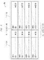
- FIG. 2 is a schematic diagram of a partial area P1 of the image DVin.
- the partial area P1 of the target image DVin is divided into rectangular tiles T1 and T2 serving as units of coding.
- the partial area P1 of the target image DVin is divided into rectangular image blocks B1 to B12 serving as units of compression.
- the area of the tile T1 is first coded and then the area of the tile T2 is coded. Specifically, first in the area of the tile T1 divided into four rows, coding is sequentially performed on an area E1 to an area E2 in the first row, an area E3 to an area E4 in the second row, an area E5 to an area E6 in the third row, and an area E7 to an area E8 in the fourth row.
- coding is sequentially performed on an area E9 to an area E10 in the first row, an area E11 to an area E12 in the second row, an area E13 to an area E14 in the third row, and an area E15 to an area E16 in the fourth row.
- the determination circuit 12 first determines whether the area of the image block B1 includes the boundary (hereinafter will be referred to as a tile boundary) X1 between the tiles T1 and T2. In this example, the determination circuit 12 determines that the area of the image block B1 does not include the tile boundary X1. Thus, the compression circuit 13 compresses the coded image block B1. The compressed image block B1 is written into the memory 17 via the bus 15. The same processing is performed on the image blocks B2 to B4.
- the determination circuit 12 determines whether the area of the image block B5 includes the tile boundary X1. In this example, the determination circuit 12 determines that the area of the image block B5 includes the tile boundary X1. Thus, in the area of the image block B5, the compression circuit 13 does not compress the image data of the area E2 (hereinafter will be referred to as image data E2) near the tile T1 coded in advance.
- image data E2 is written with dummy image data (hereinafter will be referred to as dummy data) D9 into the memory 17 via the bus 15.
- the dummy data D9 substitutes for the image data of the area E9 near the tile T2 that has not been coded yet. Thus, only the image data E2 may be written into the memory 17 without the dummy data D9.
- the same processing is performed on the image blocks B6 to B8.
- the image data of the area E9 (hereinafter will be referred to as image data E9) near the coded tile T2 is written into the memory 17 via the bus 15 without being compressed.
- image data E9 the image data of the area E9
- the dummy data D9 is overwritten with the image data E9.
- the image E2 and the dummy data D9 are stored in the memory 17 without being compressed, so that the address of the stored dummy data D9 is easily calculated.
- the image data E9 may be written into the memory 17 from the coding circuit 11 through the compression circuit 13 or may be directly written into the memory 17 from the coding circuit 11. The same processing is performed on the image blocks B6 to B8 after the completion of coding of the areas E11, E13, and E15.
- the determination circuit 12 determines that the area of the image block B9 does not include the tile boundary X1 between the tiles T1 and T2.
- the compression circuit 13 compresses the coded image block B9.
- the compressed image block B9 is written into the memory 17 via the bus 15. The same processing is performed on the image blocks B10 to B12.
- the image processor 1 and the image processing system SYS1 including the same according to the present embodiment do not compress the image block (e.g., the image block B5) including the tile boundary X1. This can eliminate the need for providing a holding circuit for holding the coding result of the tile T1 from among the tiles T1 and T2, which are formed on both sides of the tile boundary X1, until the completion of image processing on the tile T2 after the completion of image processing on the tile T1. Furthermore, the image processor 1 and the image processing system SYS1 including the same according to the present embodiment do not compress the image block (e.g., the image block B1) not including the tile boundary X1. This can suppress the consumption of a band at the bus 15 between the image processor 1 and the memory 17, achieving efficient image processing. In short, the image processor 1 and the image processing system SYS1 including the same according to the present embodiment can efficiently perform image processing without increasing the circuit size.
- the present embodiment will describe another example of determination and compression by an image processor 1.
- FIG. 3 is a schematic diagram of a partial area P2 of an image DVin to be coded.
- the partial area P2 of the target image DVin is divided into rectangular tiles T1 and T2 serving as units of coding.
- the partial area P2 of the target image DVin is divided into rectangular image blocks B1 to B8 serving as units of compression.
- a tile boundary X1 is located on the boundary between the adjacent image blocks B1 and B5.
- the tile boundary X1 is located on the boundary between the adjacent image blocks B2 and B6, on the boundary between the adjacent image blocks B3 and B7, and on the boundary between the adjacent image blocks B4 and B8.
- the area of the tile T1 is first coded and then the area of the tile T2 is coded. Specifically, first in the area of the tile T1 divided into four rows, coding is sequentially performed on an area E1 to an area E2 in the first row, an area E3 to an area E4 in the second row, an area E5 to an area E6 in the third row, and an area E7 to an area E8 in the fourth row.
- coding is sequentially performed on an area E9 to an area E10 in the first row, an area E11 to an area E12 in the second row, an area E13 to an area E14 in the third row, and an area E15 to an area E16 in the fourth row.
- a determination circuit 12 first determines that the tile boundary X1 is located on the boundary between the adjacent image blocks B1 and B5. Thus, a compression circuit 13 does not compress the coded image block B1. The uncompressed image block B1 is written into a memory 17 via a bus 15. The same processing is performed on the image blocks B2 to B4.
- a filter 119 filters a boundary area between the coded image blocks B1 and B5.
- the filtering result of an area near the image block B1 is written into the memory 17 via the bus 15.
- a boundary area at the image block B2 in the image block B1 stored in the memory 17 is overwritten with the filtering result.
- the image block B1 is stored in the memory 17 without being compressed, so that the address of a storage area overwritten with the filtering result is easily calculated.
- the filtering result may be written into the memory 17 from a coding circuit 11 through the compression circuit 13 or may be directly written into the memory 17 from the coding circuit 11.
- the same processing is performed on the image blocks B6 to B8 after the completion of filtering on boundary areas at the image blocks B2 to B4.
- the compression circuit 13 compresses the coded and filtered image block B5.
- the compressed image block B5 is written into the memory 17 via the bus 15. The same processing is performed on the image blocks B6 to B8.
- the image processor 1 and the image processing system SYS1 including the same can efficiently perform image processing without increasing the circuit size even if the tile boundary X1 is located on the boundary between the adjacent image blocks.
- the present embodiment will describe another example of determination and compression by an image processor 1.
- filtering of an image is not necessary on a tile boundary X1.
- FIG. 4 is a schematic diagram of a partial area P3 of an image DVin to be coded.
- the relationship between tiles T1 and T2 and image blocks B1 to B12 in the area P3 of FIG. 4 is similar to that of the area P1 in FIG. 2 and thus the explanation thereof is omitted.
- FIG. 5 is an image of a dummy area inserted into the partial area P3 of the target image DVin.
- FIG. 6 shows a difference in the layout of the image block on a memory depending on whether the image block is compressed or not.
- a compression circuit 13 compresses the image block regardless of whether the tile boundary X1 is included in the area of the image block to be compressed.
- the compression circuit 13 compresses the image block B5.
- the compression circuit 13 first compresses an image block B5_1 serving as a unit of compression, the image block B5_1 including the image data of an area E2 (hereinafter will be referred to as image data E2) near the tile T1 coded in advance and dummy data D9.
- image data E2 the image data of an area E2
- the compressed image block B5_1 is written into a memory 17 via a bus 15.
- image blocks B6_1, B7_1, and B8_1, which are combinations of image data E4, E6, and E8 and dummy data D11, D13, and D15, are written into the memory 17 via the bus 15.
- the compression circuit 13 compresses an image block B5_2 serving as a unit of compression at the completion of coding on an area E9 near the tile T2, the image block B5_2 including the image data of the area E9 (hereinafter will be referred to as image data E9) near the coded tile T2 and dummy data D2.
- image data E9 the image data of the area E9
- the compressed image block B5_2 is written into the memory 17 via the bus 15.
- image blocks B6_2, B7_2, and B8_2 which are combinations of image data E11, E13, and E15 and dummy data D4, D6, and D8, are written into the memory 17 via the bus 15.
- the image block B5 is read in the following steps .
- a decompression circuit 14 first reads the compressed image blocks B5_1 and B5_2 from the memory 17 via a bus 16. The decompression circuit 14 then expands the compressed image blocks B5_1 and B5_2. Subsequently, the decompression circuit 14 removes the dummy data D9 and D2 from the expanded image blocks B5_1 and B5_2 and combines the remaining image data E2 and E9 so as to reproduce image data B5.
- the starting addresses of the compressed and stored image data B5_1 and B5_2 in the memory 17 are preferably set as those of the uncompressed image data (see FIG. 6 ). This facilitates access to the image data B5_1 and B5_2.
- auxiliary information may be written, the auxiliary information including information on the division of the image data B5 into the image data B5_1 and B5_2 and the data sizes of the image blocks B5_1 and B5_2 before being combined with the dummy data D9 and D2.
- the image processor 1 and an image processing system SYS1 including the same according to the present embodiment compress, as an image block with dummy data, one of areas separated by the tile boundary X1 in the image block serving as a unit of compression and compress the other area as another image block with dummy data.
- the image processor 1 and the image processing system SYS1 including the same according to the present embodiment can suppress the consumption of a band at the bus between the image processor 1 and the memory 17, though the memory 17 requires a larger storage capacity.
- the first to third embodiments described the image processor 1 for coding images.
- the present embodiment will describe an image processor 2 for decoding a coding stream.
- FIG. 7 is a block diagram illustrating a configuration example of an image processing system (semiconductor system) SYS2.
- the image processing system SYS2 is a system for decoding and compression on a coding stream BSin.
- the image processing system SYS2 includes a decoding circuit (image processing circuit) 21, a determination circuit 22, a compression circuit 23, a decompression circuit 24, a bus 25, a bus 26, and a memory 27.
- the constituent elements of the image processing system SYS2 other than the memory 27 include the image processor (semiconductor device) 2.
- the coding circuit 21 is a section for generating an image DVout by decoding the coding stream BSin to be decoded.
- the decoding circuit 21 includes a tile division unit 211, a variable-length decoding unit 212, an inverse quantization unit 213, an inverse orthogonal transformation unit 214, an adder 215, a filter 216, and a motion prediction unit 217.
- the tile division unit 211 divides the coding stream BSin to be decoded, into multiple tiles serving as units of decoding.
- the decoding of the tiles by the decoding circuit 21 is actually performed in a segmented manner in processing blocks including each tile. For example, in HEVC (High Efficiency Video Coding), decoding is performed in CTBs (Coding Tree Blocks) including each tile. Moreover, in VP9, decoding is performed in Superblocks including each tile. As a matter of course, decoding is not always performed in CTBs or Superblocks and can be performed in other processing blocks including each tile.
- variable-length decoding unit 212 decodes, with variable lengths, the tiles sequentially outputted from the tile division unit 211 (hereinafter will be referred to as decoding target tiles), so that a quantized DCT coefficient is outputted.
- the inverse quantization unit 213 performs inverse quantization on the quantized DCT coefficient.
- the inverse orthogonal transformation unit 214 performs inverse DCT on the DCT coefficient inversely quantized by the inverse quantization unit 213, so that a differential decoding tile is outputted.
- the adder 215 adds the differential decoding tile and a corresponding prediction tile outputted from the motion prediction unit 217.
- the filter 216 filters the output result of the adder 215, so that a decoded tile (decoding tile) is outputted. For example, the filter 216 performs filtering for smoothing irregularities at tile boundaries.
- the decoding circuit 21 performs the same processing on each of the decoding target tiles including a decoding BSout to be decoded, so that an image DVout including multiple decoding tiles is outputted.
- the determination circuit 22 determines whether a tile boundary X1 is included in the image blocks serving as the units of compression of the image DVout, based on division information acquired by the tile division unit 211 and compression information acquired by the compression circuit 23.
- the division information acquired by the tile division unit 211 includes information on, for example, the positions and sizes of the tiles.
- the compression information acquired by the compression circuit 23 includes information on, for example, the positions and sizes of the image blocks. The positions and sizes of the image blocks can be acquired from the storage address of the memory 27.
- the compression circuit 23 compresses the image blocks serving as the units of compression of the image DVout, according to the determination result of the determination circuit 22. For example, if the determination circuit 22 determines that the tile boundary X1 is not included in the image block to be compressed, the compression circuit 23 compresses the image block. In contrast, if the determination circuit 22 determines that the tile boundary X1 is included in the image block to be compressed, the compression circuit 23 does not compress the image block.
- the image block compressed (or not compressed) by the compression circuit 23 is written into the memory 27 via the bus 25.
- the image block written into the memory 27 is used for inter-image prediction (inter-frame prediction) by the motion prediction unit 217 provided in the decoding circuit 21.
- the decompression circuit 24 expands the image block compressed by the compression circuit 23 from among the image blocks read from the memory 27 via the bus 26.
- the decompression circuit 24 then combines the image blocks so as to reproduce the image DVout.
- the motion prediction unit 217 In the decoding circuit 21, the motion prediction unit 217 generates the prediction image between the tiles by comparing the decoding target tile and the tile (reference tile) of an area corresponding to the decoding target tile in the image DVout, and then the motion prediction unit 217 outputs, as the prediction tile, the tile compensating for the predicted image. As described above, the prediction tile is supplied to the adder 215.
- the image processor 2 and the image processing system SYS2 including the same according to the present embodiment do not compress the image block including the tile boundary X1. This can eliminate the need for providing a holding circuit for holding the decoding result of one of two tiles, which are formed on both sides of the tile boundary X1, until the completion of image processing on one of the tiles after the completion of image processing on the other tile. Furthermore, the image processor 2 and the image processing system SYS2 including the same according to the present embodiment compress the image block not including the tile boundary X1. This can suppress the consumption of a band at the bus between the image processor 2 and the memory 27, achieving efficient image processing. In short, the image processor 2 and the image processing system SYS2 including the same according to the present embodiment can efficiently perform image processing without increasing the circuit size.
- Determination and compression by the image processor 2 according to the fourth embodiment are similar to the determination and compression by the image processor 1 according to the first to third embodiments and thus the explanation thereof is omitted.
- the image processor and the image processing system including the same according to the first to fourth embodiments do not compress the image block including the tile boundary X1. This can eliminate the need for providing a holding circuit for holding the image processing result of one of two tiles, which are formed on both sides of the tile boundary X1, until the completion of image processing on one of the tiles after the completion of image processing on the other tile. Furthermore, the image processor and the image processing system including the same according to the first to fourth embodiments compress the image block not including the tile boundary X1. This can suppress the consumption of a band at the bus between the image processor and the memory, achieving efficient image processing. In short, the image processor and the image processing system including the same according to the first to fourth embodiments can efficiently perform image processing without increasing the circuit size.
Landscapes
- Engineering & Computer Science (AREA)
- Multimedia (AREA)
- Signal Processing (AREA)
- Physics & Mathematics (AREA)
- General Physics & Mathematics (AREA)
- Discrete Mathematics (AREA)
- Theoretical Computer Science (AREA)
- Compression Or Coding Systems Of Tv Signals (AREA)
- Memory System (AREA)
Claims (6)
- Un processeur d'image comprenant :un circuit de codage (11) pour diviser une image cible (DVin) en une pluralité de carreaux, et pour coder les carreaux en unités de carreau afin de générer un flux de codage (BSout) et une image de décodage locale (LDI) ;un circuit de compression (13) pour compresser l'image de décodage local (LDI) en unités de blocs d'image ; etun circuit de détermination (12) pour déterminer si une limite de carreau est incluse dans chacun des blocs d'image de l'image de décodage local (LDI),caractérisé en ce que :la compression par le circuit de compression (13) est configurée pour être effectuée en parallèle avec le codage par le circuit de codage (11), etle circuit de compression (13) est configuré pour :si le circuit de détermination (12) détermine qu'une limite de carreau n'est pas incluse dans un bloc d'image, compresser le bloc d'image et écrire le bloc d'image compressé dans une mémoire (17), etsi le circuit de détermination (12) détermine qu'une limite de carreau est incluse dans un bloc d'image, ne pas compresser le bloc d'image, et écrire l'une des deux zones du bloc d'image non compressé qui est séparée par la limite de carreau et appartient à un carreau codé en premier dans la mémoire (17), puis écrire dans la mémoire (17) l'autre zone du bloc d'image non compressé qui est séparée par la limite de carreau et qui appartient à un deuxième carreau codé.
- Le processeur d'images selon la revendication 1, comprenant en outre :un circuit de décompression (14) pour lire les blocs d'image stockés dans la mémoire (17), étendre les blocs d'image compressés parmi les blocs d'image lus, et combiner les blocs d'image compressés et non compressés afin de reproduire l'image de décodage locale (LDI),le circuit de codage (11) étant configuré pour comparer un carreau à coder avec un carreau de référence correspondant dans l'image de décodage local (LDI) reproduite afin de générer un carreau de prédiction pour une compensation de mouvement.
- Le processeur d'images selon la revendication 1,
dans lequel si le circuit de détermination (12) détermine qu'une limite de carreau est incluse dans un bloc d'image, le circuit de compression (13) est configuré pour écrire, sans compression, en plus l'une des deux zones du bloc d'image qui est séparée par la limite de carreau et qui est déjà codée, une image factice remplaçant l'autre zone du bloc d'image qui est séparée par la limite de carreau et qui n'a pas encore été codée dans la mémoire (17) puis écraser l'image factice dans la mémoire (17) avec l'autre zone du bloc d'image qui a été codée. - Un processeur d'image comprenant :
un circuit de décodage (21) pour diviser un flux de codage (BSin) en une pluralité de carreaux, et pour décoder les carreaux en unités de carreau afin de générer une image décodée (DVout) :un circuit de compression (23) pour compresser l'image décodée (DVout) en unités de bloc d'image ; etun circuit de détermination (22) pour déterminer si une limite de carreau est incluse dans chacun des blocs d'image de l'image décodée (DVout),caractérisé en ce que :la compression par le circuit de compression (23) est configurée pour être effectuée en parallèle avec le décodage par le circuit de décodage (21), etle circuit de compression (23) est configuré pour :si le circuit de détermination (22) détermine qu'une limite de carreau n'est pas incluse dans un bloc d'image, compresser le bloc d'image et écrire le bloc d'image compressé dans une mémoire (27), etsi le circuit de détermination (22) détermine qu'une limite de carreau est incluse dans un bloc d'image, ne pas compresser le bloc d'image, et écrire l'une des deux zones du bloc d'image non compressé qui est séparée par la limite de carreau et qui appartient à un carreau décodé en premier dans la mémoire (27), puis écrire l'autre zone du bloc d'image non compressé qui est séparée par la limite de carreau et appartient à un deuxième carreau décodé dans la mémoire (27). - Le processeur d'images selon la revendication 4, comprenant en outre :un circuit de décompression (24) pour lire les blocs d'image stockés dans la mémoire (27), étendre les blocs d'image compressés parmi les blocs d'image lus, et combiner les blocs d'image compressés et non compressés afin de reproduire l'image décodée (DVout),le circuit de codage (21) étant configuré pour comparer un carreau à décoder avec un carreau de référence correspondant dans l'image décodée (DVout) reproduite afin de générer un carreau de prédiction pour une compensation de mouvement.
- Un système de traitement d'image (SYS1 ; SYS2) comprenant :un bus (15 ; 25) ;le processeur d'image (1 ; 2) selon l'une quelconque des revendications 1 à 5, le processeur d'image étant relié au bus (15 ; 25) ; etune mémoire (17 ; 27) dans laquelle un résultat de sortie du processeur d'image est écrit via le bus (15 ; 25).
Applications Claiming Priority (1)
| Application Number | Priority Date | Filing Date | Title |
|---|---|---|---|
| JP2018108454A JP7082529B2 (ja) | 2018-06-06 | 2018-06-06 | 半導体装置及び半導体装置による処理方法 |
Publications (3)
| Publication Number | Publication Date |
|---|---|
| EP3579112A2 EP3579112A2 (fr) | 2019-12-11 |
| EP3579112A3 EP3579112A3 (fr) | 2019-12-18 |
| EP3579112B1 true EP3579112B1 (fr) | 2022-07-06 |
Family
ID=66647066
Family Applications (1)
| Application Number | Title | Priority Date | Filing Date |
|---|---|---|---|
| EP19176102.2A Active EP3579112B1 (fr) | 2018-06-06 | 2019-05-23 | Dispositif semi-conducteur et procédé de traitement utilisant le dispositif semi-conducteur |
Country Status (4)
| Country | Link |
|---|---|
| US (1) | US10977834B2 (fr) |
| EP (1) | EP3579112B1 (fr) |
| JP (1) | JP7082529B2 (fr) |
| CN (1) | CN110572663B (fr) |
Families Citing this family (2)
| Publication number | Priority date | Publication date | Assignee | Title |
|---|---|---|---|---|
| DE102021117548A1 (de) | 2020-07-16 | 2022-01-20 | Samsung Electronics Co., Ltd. | Bildsensormodul, bildverarbeitungssystem, und bildkomprimierungsverfahren |
| CN117014618B (zh) * | 2023-08-07 | 2025-07-22 | 爱芯元智半导体股份有限公司 | 一种基于图像压缩的分块方法、系统及电子设备 |
Family Cites Families (14)
| Publication number | Priority date | Publication date | Assignee | Title |
|---|---|---|---|---|
| JP3948619B2 (ja) * | 2003-03-31 | 2007-07-25 | 株式会社リコー | 画像圧縮装置、画像圧縮方法、プログラム及び記録媒体 |
| JP2010098352A (ja) | 2008-10-14 | 2010-04-30 | Panasonic Corp | 画像情報符号化装置 |
| JP2010226672A (ja) | 2009-03-25 | 2010-10-07 | Nippon Hoso Kyokai <Nhk> | 画像分割装置、分割画像符号化装置及びプログラム |
| JP4703759B2 (ja) * | 2009-11-27 | 2011-06-15 | 株式会社東芝 | 画像処理装置および同装置における画像処理方法 |
| US8588536B2 (en) * | 2010-02-22 | 2013-11-19 | Texas Instruments Incorporated | Guaranteed-rate tiled image data compression |
| JP5585290B2 (ja) | 2010-08-12 | 2014-09-10 | 富士通株式会社 | 動画像符号化装置 |
| WO2012046435A1 (fr) * | 2010-10-04 | 2012-04-12 | パナソニック株式会社 | Dispositif de traitement d'images, procédé de codage d'images et procédé de traitement d'images |
| CN106941608B (zh) * | 2011-06-30 | 2021-01-15 | 三菱电机株式会社 | 图像编码装置及方法、图像解码装置及方法 |
| CN107257490B (zh) | 2012-01-27 | 2019-12-17 | 太阳专利托管公司 | 图像编码方法及图像编码装置 |
| US20130208808A1 (en) | 2012-02-08 | 2013-08-15 | Panasonic Corporation | Image coding method and image decoding method |
| US9407920B2 (en) * | 2013-01-22 | 2016-08-02 | Vixs Systems, Inc. | Video processor with reduced memory bandwidth and methods for use therewith |
| US20160092112A1 (en) * | 2014-09-25 | 2016-03-31 | Intel Corporation | Instruction and logic for hardware compression with tiled data structures of dissimilar dimensions |
| JP6605323B2 (ja) | 2015-12-24 | 2019-11-13 | ルネサスエレクトロニクス株式会社 | 半導体装置、データ処理システム及び半導体装置の制御方法 |
| CN105578190B (zh) * | 2016-02-03 | 2018-05-04 | 珠海全志科技股份有限公司 | 应用于视频硬解码的无损压缩方法及系统 |
-
2018
- 2018-06-06 JP JP2018108454A patent/JP7082529B2/ja active Active
-
2019
- 2019-05-10 US US16/409,502 patent/US10977834B2/en active Active
- 2019-05-23 EP EP19176102.2A patent/EP3579112B1/fr active Active
- 2019-05-28 CN CN201910451663.8A patent/CN110572663B/zh active Active
Also Published As
| Publication number | Publication date |
|---|---|
| EP3579112A2 (fr) | 2019-12-11 |
| EP3579112A3 (fr) | 2019-12-18 |
| US10977834B2 (en) | 2021-04-13 |
| JP2019212089A (ja) | 2019-12-12 |
| CN110572663A (zh) | 2019-12-13 |
| JP7082529B2 (ja) | 2022-06-08 |
| US20190378306A1 (en) | 2019-12-12 |
| CN110572663B (zh) | 2022-09-13 |
Similar Documents
| Publication | Publication Date | Title |
|---|---|---|
| US8576924B2 (en) | Piecewise processing of overlap smoothing and in-loop deblocking | |
| US7792385B2 (en) | Scratch pad for storing intermediate loop filter data | |
| TWI877589B (zh) | 圖像編碼裝置、圖像解碼裝置、圖像編碼方法、圖像解碼方法 | |
| US8675979B2 (en) | Transcoder, method of transcoding, and digital recorder | |
| CN107087184A (zh) | 一种多媒体数据再压缩方法 | |
| WO2007091588A1 (fr) | Dispositif de décodage d'image dynamique, dispositif d'enregistrement d'image décodée, méthode correspondante et programme | |
| TWI863883B (zh) | 圖像編碼裝置、圖像解碼裝置、方法及程式 | |
| EP3579112B1 (fr) | Dispositif semi-conducteur et procédé de traitement utilisant le dispositif semi-conducteur | |
| WO2007148619A1 (fr) | Dispositif de décodage d'image dynamique, dispositif d'enregistrement d'image décodée et procédé et programme associés | |
| US7432835B2 (en) | Variable length decoding method and device | |
| US20110249959A1 (en) | Video storing method and device based on variable bit allocation and related video encoding and decoding apparatuses | |
| JPH1023411A (ja) | 画像符号化方法、画像信号記録媒体及び画像復号装置 | |
| JPH10224790A (ja) | 圧縮伸張された画像中のブロック状ノイズを除去するフィルタおよびフィルタ方法 | |
| JP7359653B2 (ja) | 動画像符号化装置 | |
| US20230057659A1 (en) | Encoder, method, and non-transitory computer-readable storage medium | |
| TWI853577B (zh) | 圖像編碼裝置、圖像解碼裝置、圖像編碼方法、圖像解碼方法 | |
| US20170094280A1 (en) | Semiconductor device | |
| JP2023030585A5 (fr) | ||
| JP7020782B2 (ja) | 再生装置及びその制御方法 | |
| JP2914320B2 (ja) | モジュール切り替え型画像圧縮・再生装置 | |
| JPH0522709A (ja) | 画像信号復号化装置 | |
| JP2812203B2 (ja) | 画像再生装置 | |
| CN100396101C (zh) | 产生并使用辅助图像的图像压缩设备及其方法 | |
| JP3332220B2 (ja) | ディジタル信号再生装置及び再生方法 | |
| HK40093827A (zh) | 图像解码方法、编码方法及装置 |
Legal Events
| Date | Code | Title | Description |
|---|---|---|---|
| PUAI | Public reference made under article 153(3) epc to a published international application that has entered the european phase |
Free format text: ORIGINAL CODE: 0009012 |
|
| STAA | Information on the status of an ep patent application or granted ep patent |
Free format text: STATUS: THE APPLICATION HAS BEEN PUBLISHED |
|
| PUAL | Search report despatched |
Free format text: ORIGINAL CODE: 0009013 |
|
| AK | Designated contracting states |
Kind code of ref document: A2 Designated state(s): AL AT BE BG CH CY CZ DE DK EE ES FI FR GB GR HR HU IE IS IT LI LT LU LV MC MK MT NL NO PL PT RO RS SE SI SK SM TR |
|
| AX | Request for extension of the european patent |
Extension state: BA ME |
|
| AK | Designated contracting states |
Kind code of ref document: A3 Designated state(s): AL AT BE BG CH CY CZ DE DK EE ES FI FR GB GR HR HU IE IS IT LI LT LU LV MC MK MT NL NO PL PT RO RS SE SI SK SM TR |
|
| AX | Request for extension of the european patent |
Extension state: BA ME |
|
| RIC1 | Information provided on ipc code assigned before grant |
Ipc: G06K 9/36 20060101ALI20191108BHEP Ipc: G06F 13/00 20060101AFI20191108BHEP Ipc: G06T 1/60 20060101ALI20191108BHEP |
|
| STAA | Information on the status of an ep patent application or granted ep patent |
Free format text: STATUS: REQUEST FOR EXAMINATION WAS MADE |
|
| 17P | Request for examination filed |
Effective date: 20200618 |
|
| RBV | Designated contracting states (corrected) |
Designated state(s): AL AT BE BG CH CY CZ DE DK EE ES FI FR GB GR HR HU IE IS IT LI LT LU LV MC MK MT NL NO PL PT RO RS SE SI SK SM TR |
|
| STAA | Information on the status of an ep patent application or granted ep patent |
Free format text: STATUS: EXAMINATION IS IN PROGRESS |
|
| 17Q | First examination report despatched |
Effective date: 20210506 |
|
| REG | Reference to a national code |
Ref country code: DE Ref legal event code: R079 Ref document number: 602019016609 Country of ref document: DE Free format text: PREVIOUS MAIN CLASS: G06F0013000000 Ipc: H04N0019122000 |
|
| GRAP | Despatch of communication of intention to grant a patent |
Free format text: ORIGINAL CODE: EPIDOSNIGR1 |
|
| STAA | Information on the status of an ep patent application or granted ep patent |
Free format text: STATUS: GRANT OF PATENT IS INTENDED |
|
| RIC1 | Information provided on ipc code assigned before grant |
Ipc: H04N 19/625 20140101ALI20220131BHEP Ipc: H04N 19/426 20140101ALI20220131BHEP Ipc: H04N 19/174 20140101ALI20220131BHEP Ipc: H04N 19/122 20140101AFI20220131BHEP |
|
| INTG | Intention to grant announced |
Effective date: 20220225 |
|
| GRAS | Grant fee paid |
Free format text: ORIGINAL CODE: EPIDOSNIGR3 |
|
| GRAA | (expected) grant |
Free format text: ORIGINAL CODE: 0009210 |
|
| STAA | Information on the status of an ep patent application or granted ep patent |
Free format text: STATUS: THE PATENT HAS BEEN GRANTED |
|
| AK | Designated contracting states |
Kind code of ref document: B1 Designated state(s): AL AT BE BG CH CY CZ DE DK EE ES FI FR GB GR HR HU IE IS IT LI LT LU LV MC MK MT NL NO PL PT RO RS SE SI SK SM TR |
|
| REG | Reference to a national code |
Ref country code: AT Ref legal event code: REF Ref document number: 1503714 Country of ref document: AT Kind code of ref document: T Effective date: 20220715 Ref country code: CH Ref legal event code: EP |
|
| REG | Reference to a national code |
Ref country code: DE Ref legal event code: R096 Ref document number: 602019016609 Country of ref document: DE |
|
| REG | Reference to a national code |
Ref country code: IE Ref legal event code: FG4D |
|
| REG | Reference to a national code |
Ref country code: LT Ref legal event code: MG9D |
|
| REG | Reference to a national code |
Ref country code: NL Ref legal event code: MP Effective date: 20220706 |
|
| PG25 | Lapsed in a contracting state [announced via postgrant information from national office to epo] |
Ref country code: SE Free format text: LAPSE BECAUSE OF FAILURE TO SUBMIT A TRANSLATION OF THE DESCRIPTION OR TO PAY THE FEE WITHIN THE PRESCRIBED TIME-LIMIT Effective date: 20220706 Ref country code: RS Free format text: LAPSE BECAUSE OF FAILURE TO SUBMIT A TRANSLATION OF THE DESCRIPTION OR TO PAY THE FEE WITHIN THE PRESCRIBED TIME-LIMIT Effective date: 20220706 Ref country code: PT Free format text: LAPSE BECAUSE OF FAILURE TO SUBMIT A TRANSLATION OF THE DESCRIPTION OR TO PAY THE FEE WITHIN THE PRESCRIBED TIME-LIMIT Effective date: 20221107 Ref country code: NO Free format text: LAPSE BECAUSE OF FAILURE TO SUBMIT A TRANSLATION OF THE DESCRIPTION OR TO PAY THE FEE WITHIN THE PRESCRIBED TIME-LIMIT Effective date: 20221006 Ref country code: NL Free format text: LAPSE BECAUSE OF FAILURE TO SUBMIT A TRANSLATION OF THE DESCRIPTION OR TO PAY THE FEE WITHIN THE PRESCRIBED TIME-LIMIT Effective date: 20220706 Ref country code: LV Free format text: LAPSE BECAUSE OF FAILURE TO SUBMIT A TRANSLATION OF THE DESCRIPTION OR TO PAY THE FEE WITHIN THE PRESCRIBED TIME-LIMIT Effective date: 20220706 Ref country code: LT Free format text: LAPSE BECAUSE OF FAILURE TO SUBMIT A TRANSLATION OF THE DESCRIPTION OR TO PAY THE FEE WITHIN THE PRESCRIBED TIME-LIMIT Effective date: 20220706 Ref country code: FI Free format text: LAPSE BECAUSE OF FAILURE TO SUBMIT A TRANSLATION OF THE DESCRIPTION OR TO PAY THE FEE WITHIN THE PRESCRIBED TIME-LIMIT Effective date: 20220706 Ref country code: ES Free format text: LAPSE BECAUSE OF FAILURE TO SUBMIT A TRANSLATION OF THE DESCRIPTION OR TO PAY THE FEE WITHIN THE PRESCRIBED TIME-LIMIT Effective date: 20220706 |
|
| REG | Reference to a national code |
Ref country code: AT Ref legal event code: MK05 Ref document number: 1503714 Country of ref document: AT Kind code of ref document: T Effective date: 20220706 |
|
| PG25 | Lapsed in a contracting state [announced via postgrant information from national office to epo] |
Ref country code: PL Free format text: LAPSE BECAUSE OF FAILURE TO SUBMIT A TRANSLATION OF THE DESCRIPTION OR TO PAY THE FEE WITHIN THE PRESCRIBED TIME-LIMIT Effective date: 20220706 Ref country code: IS Free format text: LAPSE BECAUSE OF FAILURE TO SUBMIT A TRANSLATION OF THE DESCRIPTION OR TO PAY THE FEE WITHIN THE PRESCRIBED TIME-LIMIT Effective date: 20221106 Ref country code: HR Free format text: LAPSE BECAUSE OF FAILURE TO SUBMIT A TRANSLATION OF THE DESCRIPTION OR TO PAY THE FEE WITHIN THE PRESCRIBED TIME-LIMIT Effective date: 20220706 Ref country code: GR Free format text: LAPSE BECAUSE OF FAILURE TO SUBMIT A TRANSLATION OF THE DESCRIPTION OR TO PAY THE FEE WITHIN THE PRESCRIBED TIME-LIMIT Effective date: 20221007 |
|
| REG | Reference to a national code |
Ref country code: DE Ref legal event code: R097 Ref document number: 602019016609 Country of ref document: DE |
|
| PG25 | Lapsed in a contracting state [announced via postgrant information from national office to epo] |
Ref country code: SM Free format text: LAPSE BECAUSE OF FAILURE TO SUBMIT A TRANSLATION OF THE DESCRIPTION OR TO PAY THE FEE WITHIN THE PRESCRIBED TIME-LIMIT Effective date: 20220706 Ref country code: RO Free format text: LAPSE BECAUSE OF FAILURE TO SUBMIT A TRANSLATION OF THE DESCRIPTION OR TO PAY THE FEE WITHIN THE PRESCRIBED TIME-LIMIT Effective date: 20220706 Ref country code: DK Free format text: LAPSE BECAUSE OF FAILURE TO SUBMIT A TRANSLATION OF THE DESCRIPTION OR TO PAY THE FEE WITHIN THE PRESCRIBED TIME-LIMIT Effective date: 20220706 Ref country code: CZ Free format text: LAPSE BECAUSE OF FAILURE TO SUBMIT A TRANSLATION OF THE DESCRIPTION OR TO PAY THE FEE WITHIN THE PRESCRIBED TIME-LIMIT Effective date: 20220706 Ref country code: AT Free format text: LAPSE BECAUSE OF FAILURE TO SUBMIT A TRANSLATION OF THE DESCRIPTION OR TO PAY THE FEE WITHIN THE PRESCRIBED TIME-LIMIT Effective date: 20220706 |
|
| PLBE | No opposition filed within time limit |
Free format text: ORIGINAL CODE: 0009261 |
|
| STAA | Information on the status of an ep patent application or granted ep patent |
Free format text: STATUS: NO OPPOSITION FILED WITHIN TIME LIMIT |
|
| PG25 | Lapsed in a contracting state [announced via postgrant information from national office to epo] |
Ref country code: SK Free format text: LAPSE BECAUSE OF FAILURE TO SUBMIT A TRANSLATION OF THE DESCRIPTION OR TO PAY THE FEE WITHIN THE PRESCRIBED TIME-LIMIT Effective date: 20220706 Ref country code: EE Free format text: LAPSE BECAUSE OF FAILURE TO SUBMIT A TRANSLATION OF THE DESCRIPTION OR TO PAY THE FEE WITHIN THE PRESCRIBED TIME-LIMIT Effective date: 20220706 |
|
| 26N | No opposition filed |
Effective date: 20230411 |
|
| PG25 | Lapsed in a contracting state [announced via postgrant information from national office to epo] |
Ref country code: AL Free format text: LAPSE BECAUSE OF FAILURE TO SUBMIT A TRANSLATION OF THE DESCRIPTION OR TO PAY THE FEE WITHIN THE PRESCRIBED TIME-LIMIT Effective date: 20220706 |
|
| PG25 | Lapsed in a contracting state [announced via postgrant information from national office to epo] |
Ref country code: SI Free format text: LAPSE BECAUSE OF FAILURE TO SUBMIT A TRANSLATION OF THE DESCRIPTION OR TO PAY THE FEE WITHIN THE PRESCRIBED TIME-LIMIT Effective date: 20220706 |
|
| REG | Reference to a national code |
Ref country code: CH Ref legal event code: PL |
|
| PG25 | Lapsed in a contracting state [announced via postgrant information from national office to epo] |
Ref country code: MC Free format text: LAPSE BECAUSE OF FAILURE TO SUBMIT A TRANSLATION OF THE DESCRIPTION OR TO PAY THE FEE WITHIN THE PRESCRIBED TIME-LIMIT Effective date: 20220706 |
|
| GBPC | Gb: european patent ceased through non-payment of renewal fee |
Effective date: 20230523 |
|
| REG | Reference to a national code |
Ref country code: BE Ref legal event code: MM Effective date: 20230531 |
|
| PG25 | Lapsed in a contracting state [announced via postgrant information from national office to epo] |
Ref country code: MC Free format text: LAPSE BECAUSE OF FAILURE TO SUBMIT A TRANSLATION OF THE DESCRIPTION OR TO PAY THE FEE WITHIN THE PRESCRIBED TIME-LIMIT Effective date: 20220706 Ref country code: LU Free format text: LAPSE BECAUSE OF NON-PAYMENT OF DUE FEES Effective date: 20230523 Ref country code: LI Free format text: LAPSE BECAUSE OF NON-PAYMENT OF DUE FEES Effective date: 20230531 Ref country code: IT Free format text: LAPSE BECAUSE OF FAILURE TO SUBMIT A TRANSLATION OF THE DESCRIPTION OR TO PAY THE FEE WITHIN THE PRESCRIBED TIME-LIMIT Effective date: 20220706 Ref country code: CH Free format text: LAPSE BECAUSE OF NON-PAYMENT OF DUE FEES Effective date: 20230531 |
|
| REG | Reference to a national code |
Ref country code: IE Ref legal event code: MM4A |
|
| PG25 | Lapsed in a contracting state [announced via postgrant information from national office to epo] |
Ref country code: IE Free format text: LAPSE BECAUSE OF NON-PAYMENT OF DUE FEES Effective date: 20230523 |
|
| PG25 | Lapsed in a contracting state [announced via postgrant information from national office to epo] |
Ref country code: IE Free format text: LAPSE BECAUSE OF NON-PAYMENT OF DUE FEES Effective date: 20230523 Ref country code: GB Free format text: LAPSE BECAUSE OF NON-PAYMENT OF DUE FEES Effective date: 20230523 |
|
| PG25 | Lapsed in a contracting state [announced via postgrant information from national office to epo] |
Ref country code: FR Free format text: LAPSE BECAUSE OF NON-PAYMENT OF DUE FEES Effective date: 20230531 Ref country code: BE Free format text: LAPSE BECAUSE OF NON-PAYMENT OF DUE FEES Effective date: 20230531 |
|
| PG25 | Lapsed in a contracting state [announced via postgrant information from national office to epo] |
Ref country code: BG Free format text: LAPSE BECAUSE OF FAILURE TO SUBMIT A TRANSLATION OF THE DESCRIPTION OR TO PAY THE FEE WITHIN THE PRESCRIBED TIME-LIMIT Effective date: 20220706 |
|
| PG25 | Lapsed in a contracting state [announced via postgrant information from national office to epo] |
Ref country code: BG Free format text: LAPSE BECAUSE OF FAILURE TO SUBMIT A TRANSLATION OF THE DESCRIPTION OR TO PAY THE FEE WITHIN THE PRESCRIBED TIME-LIMIT Effective date: 20220706 |
|
| PGFP | Annual fee paid to national office [announced via postgrant information from national office to epo] |
Ref country code: DE Payment date: 20250528 Year of fee payment: 7 |
|
| PG25 | Lapsed in a contracting state [announced via postgrant information from national office to epo] |
Ref country code: CY Free format text: LAPSE BECAUSE OF FAILURE TO SUBMIT A TRANSLATION OF THE DESCRIPTION OR TO PAY THE FEE WITHIN THE PRESCRIBED TIME-LIMIT; INVALID AB INITIO Effective date: 20190523 |
|
| PG25 | Lapsed in a contracting state [announced via postgrant information from national office to epo] |
Ref country code: HU Free format text: LAPSE BECAUSE OF FAILURE TO SUBMIT A TRANSLATION OF THE DESCRIPTION OR TO PAY THE FEE WITHIN THE PRESCRIBED TIME-LIMIT; INVALID AB INITIO Effective date: 20190523 |
|
| PG25 | Lapsed in a contracting state [announced via postgrant information from national office to epo] |
Ref country code: TR Free format text: LAPSE BECAUSE OF FAILURE TO SUBMIT A TRANSLATION OF THE DESCRIPTION OR TO PAY THE FEE WITHIN THE PRESCRIBED TIME-LIMIT Effective date: 20220706 |