EP3579152A1 - Rechenvorrichtung und zugehöriges produkt - Google Patents
Rechenvorrichtung und zugehöriges produkt Download PDFInfo
- Publication number
- EP3579152A1 EP3579152A1 EP18787049.8A EP18787049A EP3579152A1 EP 3579152 A1 EP3579152 A1 EP 3579152A1 EP 18787049 A EP18787049 A EP 18787049A EP 3579152 A1 EP3579152 A1 EP 3579152A1
- Authority
- EP
- European Patent Office
- Prior art keywords
- vector
- instruction
- data
- sparse
- unit
- Prior art date
- Legal status (The legal status is an assumption and is not a legal conclusion. Google has not performed a legal analysis and makes no representation as to the accuracy of the status listed.)
- Granted
Links
Images


Classifications
-
- G—PHYSICS
- G06—COMPUTING OR CALCULATING; COUNTING
- G06F—ELECTRIC DIGITAL DATA PROCESSING
- G06F9/00—Arrangements for program control, e.g. control units
- G06F9/06—Arrangements for program control, e.g. control units using stored programs, i.e. using an internal store of processing equipment to receive or retain programs
- G06F9/30—Arrangements for executing machine instructions, e.g. instruction decode
- G06F9/30003—Arrangements for executing specific machine instructions
- G06F9/30007—Arrangements for executing specific machine instructions to perform operations on data operands
- G06F9/3001—Arithmetic instructions
-
- G—PHYSICS
- G06—COMPUTING OR CALCULATING; COUNTING
- G06F—ELECTRIC DIGITAL DATA PROCESSING
- G06F9/00—Arrangements for program control, e.g. control units
- G06F9/06—Arrangements for program control, e.g. control units using stored programs, i.e. using an internal store of processing equipment to receive or retain programs
- G06F9/30—Arrangements for executing machine instructions, e.g. instruction decode
- G06F9/30003—Arrangements for executing specific machine instructions
- G06F9/30007—Arrangements for executing specific machine instructions to perform operations on data operands
- G06F9/30036—Instructions to perform operations on packed data, e.g. vector, tile or matrix operations
-
- G—PHYSICS
- G06—COMPUTING OR CALCULATING; COUNTING
- G06N—COMPUTING ARRANGEMENTS BASED ON SPECIFIC COMPUTATIONAL MODELS
- G06N3/00—Computing arrangements based on biological models
- G06N3/02—Neural networks
- G06N3/04—Architecture, e.g. interconnection topology
- G06N3/045—Combinations of networks
-
- G—PHYSICS
- G06—COMPUTING OR CALCULATING; COUNTING
- G06N—COMPUTING ARRANGEMENTS BASED ON SPECIFIC COMPUTATIONAL MODELS
- G06N3/00—Computing arrangements based on biological models
- G06N3/02—Neural networks
- G06N3/04—Architecture, e.g. interconnection topology
- G06N3/0464—Convolutional networks [CNN, ConvNet]
-
- G—PHYSICS
- G06—COMPUTING OR CALCULATING; COUNTING
- G06N—COMPUTING ARRANGEMENTS BASED ON SPECIFIC COMPUTATIONAL MODELS
- G06N3/00—Computing arrangements based on biological models
- G06N3/02—Neural networks
- G06N3/04—Architecture, e.g. interconnection topology
- G06N3/048—Activation functions
-
- G—PHYSICS
- G06—COMPUTING OR CALCULATING; COUNTING
- G06N—COMPUTING ARRANGEMENTS BASED ON SPECIFIC COMPUTATIONAL MODELS
- G06N3/00—Computing arrangements based on biological models
- G06N3/02—Neural networks
- G06N3/04—Architecture, e.g. interconnection topology
- G06N3/0495—Quantised networks; Sparse networks; Compressed networks
-
- G—PHYSICS
- G06—COMPUTING OR CALCULATING; COUNTING
- G06N—COMPUTING ARRANGEMENTS BASED ON SPECIFIC COMPUTATIONAL MODELS
- G06N3/00—Computing arrangements based on biological models
- G06N3/02—Neural networks
- G06N3/06—Physical realisation, i.e. hardware implementation of neural networks, neurons or parts of neurons
- G06N3/063—Physical realisation, i.e. hardware implementation of neural networks, neurons or parts of neurons using electronic means
-
- G—PHYSICS
- G06—COMPUTING OR CALCULATING; COUNTING
- G06N—COMPUTING ARRANGEMENTS BASED ON SPECIFIC COMPUTATIONAL MODELS
- G06N3/00—Computing arrangements based on biological models
- G06N3/02—Neural networks
- G06N3/08—Learning methods
-
- G—PHYSICS
- G06—COMPUTING OR CALCULATING; COUNTING
- G06N—COMPUTING ARRANGEMENTS BASED ON SPECIFIC COMPUTATIONAL MODELS
- G06N3/00—Computing arrangements based on biological models
- G06N3/02—Neural networks
- G06N3/08—Learning methods
- G06N3/082—Learning methods modifying the architecture, e.g. adding, deleting or silencing nodes or connections
Definitions
- the present application relates to an artificial intelligence technical field, and particularly relates to an operation device and related products.
- the concept of deep learning stems from studies of artificial neural networks.
- a multilayer perceptron with multiple hidden layers is a deep-learning structure.
- the deep learning forms a more abstract high level representing attribute categories or features, to discover a distributed feature representation of data.
- the embodiments of the present application provide an operation device and related products capable of reducing storage resource and operation resource consumption in the deep learning.
- the embodiments of the present invention provides an operation device which comprises a storage unit, an operation unit, and a controller unit, wherein the storage unit is configured to store data and instructions; the controller unit is configured to extract, from the storage unit, a first instruction including sorting instructions or sparse processing instructions and a first data corresponding to the first instruction including input neuron data and weight data; the operation unit is configured to, in response to the first instruction, perform an operation corresponding to the first instruction on the input neuron data and the weight data, to obtain an operation result.
- the storage unit is configured to store data and instructions
- the controller unit is configured to extract, from the storage unit, a first instruction including sorting instructions or sparse processing instructions and a first data corresponding to the first instruction including input neuron data and weight data
- the operation unit is configured to, in response to the first instruction, perform an operation corresponding to the first instruction on the input neuron data and the weight data, to obtain an operation result.
- the embodiments of the present application provide an operation method applied to the operation device which comprises a storage unit, an operation unit, and a controller unit, wherein the storage unit is configured to store data and instructions; the controller unit is configured to extract, from the storage unit, a first instruction including sorting instructions or sparse processing instructions and a first data corresponding to the first instruction including input neuron data and weight data; the operation unit is configured to, in response to the first instruction, perform an operation corresponding to the first instruction on the input neuron data and the weight data, to obtain an operation result.
- the storage unit is configured to store data and instructions
- the controller unit is configured to extract, from the storage unit, a first instruction including sorting instructions or sparse processing instructions and a first data corresponding to the first instruction including input neuron data and weight data
- the operation unit is configured to, in response to the first instruction, perform an operation corresponding to the first instruction on the input neuron data and the weight data, to obtain an operation result.
- the embodiments of the present application provide a neural network calculating device which includes one or more operation devices according to the first aspect, wherein the neural network calculating device is configured to acquire data to be operated and control information from other processing devices, perform specified neural network operation and transmit the execution result to other processing devices through the I/O interface; when the neural network calculating device contains a plurality of said operation devices, the plurality of operation devices may be connected via a specific structure and transmit data; wherein, the plurality of operation devices conduct interconnect through Peripheral Component Interconnect-Express (PCI-E or PCIe) PCIE bus and transmit data to support operation on a larger-scale neural network; the plurality of operation devices share the same control system or have their own control systems; the plurality of the operation devices share a memory or have their own memories; and the interconnection manner of the plurality of operation devices is an arbitrary interconnection topology.
- PCI-E or PCIe Peripheral Component Interconnect-Express
- the embodiments of the present application provide a combined processing device which includes the operation device, the universal interconnect interface and other processing devices according to the first aspect.
- the neural network calculating device interacts with other processing devices described above to perform user-specified operations.
- the embodiments of the present application provide a neural network chip which includes the operation device according to the first aspect, the neural network calculating device according to the third aspect or the combined processing device according to the fourth aspect.
- the embodiments of the present application provide a neural network chip package structure which includes the neural network chip according to the fifth aspect;
- the embodiment of the present application provides a board card which includes the neural network chip package structure according to the sixth aspect.
- the embodiments of the present application provide an electronic device which includes the neural network chip according to the sixth aspect or the board card according to the seventh aspect.
- the storage unit stores data and instructions
- a controller unit configured to extract, from the storage unit, a first instruction including sorting instructions or sparse processing instructions and a first data corresponding to the first instruction including input neuron data and weight data and the operation unit performs a calculating operation corresponding to the first instruction on the input neuron data and the weight data in response to the first instruction to obtain an operation result, thereby reducing the storage resource and operation resource consumption in the deep learning and improving the operation efficiency.
- the electronic device includes a data processing device, a robot, a computer, a printer, a scanner, a tablet PC, an intelligent terminal, a mobile phone, an automobile data recorder, a navigator, a sensor, a camera, a server, a cloud server, a video camera, a projector, a watch, an earphone, a movable storage, a wearable device, a vehicle, a household appliance and/or a medical device.
- a data processing device a robot, a computer, a printer, a scanner, a tablet PC, an intelligent terminal, a mobile phone, an automobile data recorder, a navigator, a sensor, a camera, a server, a cloud server, a video camera, a projector, a watch, an earphone, a movable storage, a wearable device, a vehicle, a household appliance and/or a medical device.
- the vehicle includes an airplane, a ship and/or a car
- the household appliance includes a television, an air conditioner, a microwave oven, a refrigerator, a rice cooker, a humidifier, a washing machine, an electric lamp, a gas stove, a range hood
- the medical device includes nuclear magnetic resonance, B-ultrasonic and/or electrocardiographs.
- an operation device comprising: a storage unit 10, a controller unit 11 and an operation unit 12, wherein the controller unit 11 and the storage unit 10 and the operation unit 12;
- the storage unit 10 may include a data input/output unit (data I/O unit) 203, the data input/output unit 203 is configured to acquire input data, weight data, a network model, and operation instructions;
- the controller unit 11 is configured to extract a first instruction from the storage unit, parse the first instruction to obtain an operation code of the operation instruction and an operation domain, extract input data and weight data corresponding to the operation domain, and the operation code, the input data and the weight data are transmitted to the operation unit, and
- the operation code includes at least one of the following codes: an operation code of the matrix operation instruction, a vector operation instruction operation code, an activation operation instruction operation code, an offset operation instruction operation code, a convolution operation instruction operation code, a conversion operation instruction operation code and the like;
- the operation unit 12 is configured to extract a first instruction from the storage unit, parse the first
- the controller unit includes an instruction buffer unit 110 configured to buffer the instructions, an instruction processing unit 111 configured to implement decoding function and a storage queue unit 113; the instruction buffer unit 110 is configured to buffer the first instruction; the instruction processing unit 111 is configured to parse the first instruction to obtain an operation code of the first instruction and an operation domain; the storage queue unit 113 is configured to store an instruction queue including a plurality of operation instructions or operation codes to be performed in a sequential order of that queue.
- the operation instructions may include one or more operational domains and an operation code.
- the operation instructions may include neural network operational instructions. Taking the neural network operation instruction as an example, as shown in Table 1, the register number 0, the register number 1, the register number 2, the register number 3, and the register number 4 therein may be taken as an operation domain and each register number 0, register number 1, register number 2, register number 3, and register number 4 therein may be taken as the number of one or more registers.
- OPERATION CODE register number 0 register number 1 register number 2 register number 3 register number 4 COMPUTE input data initial address input data length weight value initial address weight value length interpolation table address of activation function IO address of external data memory data length address of inner data memory NOP JUMP target address MOVE input address data size output address
- the storage unit may further include a register 201, a buffer 202 and a data I/O unit.
- the storage medium 201 may be an off-chip memory, and of course in an actual application, may also be an on-chip memory for storing data blocks.
- the above first instruction may be a vector instruction which may be at least one of a vector addition instruction (VA), a vector plus scalar instruction (VAS), a vector subtraction instruction (VS), and a vector multiplication instruction (VMV), a vector multiplying scalar instruction (VMS), vector division instruction (VD), a vector dividing scalar instruction (SDV), an inter-vector AND instruction (VAV), an inter-vector AND instruction (VAND), an inter-vector OR instruction (VOV), an intra-vector OR instruction (VOR), a vector index instruction (VE), a vector logarithmic instruction (VL), a vector greater-than decision instruction (VGT), a vector equal-to decision instruction (VEQ), a vector NOT instruction (VINV), a vector selection and merge instruction (VMER), a vector maximum instruction (VMAX), a scalar extended instruction (STV), a scalar-vector replacement instruction (STVPN), a vector-scalar replacement instruction (VPNTS
- FIG. 1B is a modified structure of the operation device described in FIG. 1A , and the operation device may further include a configuration parsing unit 13, a mapping unit 14 and a sparse unit 15 as compared with FIG. 1A , specifically:
- the data may include at least one of the following data types: integer data, discrete data, continuous data, power type data, floating point data, or fixed point data, and the length represented by data may be a 32-bit length floating point number, a16-bit length fixed point data and the like; the data may include at least one of the following data: the input neuron data, the weight data, and the offset data.
- the configuration parsing unit 13 is configured to set a mapping mode according to the preset configuration data
- the mapping unit 14 is configured to perform mapping processing on the input neuron and the weight data according to the mapping mode to obtain an input neuron-weight pair which is a mapping relationship between the input neuron data and the weight data after mapping processing
- the instruction buffer unit 110 is configured to receive a target instruction transmitted by the controller unit
- the instruction processing unit 111 is configured to decode the target instruction into an operation instruction, and performs a calculating operation on the input neuron-weight pair by the operation unit to obtain an operation result
- the preset configuration data may include at least one of data types or sparse parameters.
- the target instruction is a matrix multiplying by a matrix calculation instruction, which is decoded to obtain an operation instruction, and the operation instruction may include a multiplication operation instruction and an addition operation instruction.
- the first instruction includes at least one target instruction.
- the sparse unit 15 is configured to perform a sparse processing on the operation result according to the sparse parameters to obtain an operation result after the sparse processing.
- the sparse parameters include a sparse mode
- the mapping unit 13 performs a mapping processing on the input neuron and the weight according to the mapping mode, specifically:
- the sparse parameters may include at least one of the following: a sparse flag, a sparse rate, a sparse mode, and the like, wherein the sparse flag is used to determine whether it is possible to perform a sparse processing, for example, 0 represents not performing a sparse processing, 1 represents performing a sparse processing; or 1 represents not performing a sparse processing, 0 represents performing a sparse processing instead. It can be understood that it is also possible to flexibly select the representation of the sparse flag according to the demand.
- the sparse rate indicates the ratio of the neuron data and/or the weight data each time the sparse processing is performed, for example, 5%, 10%, 25% and the like.
- the sparse mode represents a specific mode of sparse processing.
- the sparse mode mainly includes at least three types: a sparse mode 1 where only taking sparse processing to the weight, a sparse mode 2 where only taking sparse processing to the neuron data and a sparse mode 3 where taking sparse processing to the weight and the neuron data.
- the sparse mode can also be combined by at least two of the above modes, for example, sparse mode 1 + sparse mode 2.
- the sparse rate of the neuron data and the sparse rate of the weight data may be different, for example, the embodiments of the present application provides a representation of the sparse rate (A, B), where A is the sparse rate of the neuron data, B is the sparse rate of the weight data, for example, (5%, 6%), that is, the sparse rate of the neuron data is 5% and the sparse rate of the weight data is 6%.
- At least the following four sparse modes are included: a sparse mode 0 where no sparse is performed; a sparse mode 1 where only taking sparse processing to the weight data; a sparse mode 2 where only taking sparse processing to the neuron data; a sparse mode 3 where taking sparse processing to the weight and neuron data.
- the sparse mode obtained by parsing the configuration data of the neural network by the configuration parsing unit 13 further sets the processing mode of the mapping unit, that is, corresponding to different mapping modes according to different sparse modes.
- mapping relationship between the sparse mode and the mapping mode is pre-stored in the storage unit, and then the mapping mode corresponding to the sparse mode is determined according to the mapping relationship, and the sparse is carried out according to the neuron sparse sequence and the weight sparse sequence in different mapping modes.
- the mapping relationship is not necessarily stored in the storage unit but may be stored on the off-chip memory, or may be stored on other devices (electronic devices having storage functions).
- the weight sparse sequence and/or the neuron sparse sequence may be pre-stored in the storage unit.
- the sparse unit 15 performs sparse processing on the operation result according to the sparse parameters, specifically:
- the sparse unit 15 performs a sparse processing on the operation result according to the sparse parameters, specifically:
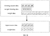
- FIG. 1C is an exemplary diagram of sparse mode 1, wherein the sparse weight data only includes non-zero data in the weight and only the weight data of w1, w5, w8, and w9 are stored, and the weight sparse sequence is used to index the sparse weights, for example, the weight sparse sequence is 100010011, indicating the weights of w1, w5, w8 and w9 are non-zero values, and those of w2, w3, w4, w6 and w7 are 0.
- the representation of the sparse sequences is not unique, 0 can be used to represent non-sparse, that is, the value is non-zero, and 1 is used to represent sparse, that is, the value is zero, and other feasible methods can also be used.
- the corresponding input neuron data is selected, and d1, d5, d8, and d9 are selected as input neuron data in FIG. 1C , and the corresponding input neuron-weight pair is obtained by mapping the input neuron data and the weight data.
- FIG. ID is an exemplary diagram of the sparse mode 2 provided by the embodiments of the present application, in which the sparse neuron data includes only non-zero data in the neuron, and only neuron data of d1, d3, d5, d8 are stored, as in FIG. ID, the neuron sparse sequence is used to index sparse neuron data, such as neuron sparse sequence 101010010 indicates that neurons of d1, d3, d5, d8 are non-zero, and those of d2, d4, d6, d7, d9 are 0.
- the representation of the sparse sequence is not unique, and 0 can be used to indicate non-sparse, that is, the value is non-zero, and 1 represents sparse, that is, the value is zero, and other feasible methods can also be used.
- the corresponding weight data is selected according to the neuron sparse sequence, for example, the weight data of w1, w3, w5, w8 are selected as shown in FIG. ID, and the input neuron data and the weight data are mapped to obtain corresponding input neuron-weight pairs.
- FIG. IE is an exemplary diagram of a sparse mode 3 according to the embodiments of the present application, that is, input neuron data and weight data are selected to be non-zero values according to a neuron sparse sequence and a weight sparse sequence.
- the neuron data d1, d5, d8 and the weight data w1, w5, w8 are selected to obtain the corresponding input neuron-weight pair by mapping the input neuron data and the weight data.
- the operation method may be implemented as follows:
- controller unit 11 includes an instruction buffer unit 110 and an instruction processing unit 111.
- the first instruction is the sparse processing instruction and the first data further includes preset configuration data
- the configuration parsing unit 13 sets a mapping mode according to the preset configuration data
- the mapping unit 14 performs mapping processing on the input neuron and the weight data according to the mapping mode to obtain an input neuron-weight pair which is a mapping relationship between the input neuron data and the weight data after the mapping processing
- the instruction buffer unit 110 receives a target instruction transmitted by the controller unit
- the instruction processing unit 111 decodes the target instruction into an operation instruction
- the operation unit 12 performs a calculating operation on the input neuron-weight pair to obtain an operation result.
- the first data further includes sparse parameters; and the method further includes the following steps: the sparse unit 15 performs sparse processing on the operation result according to the sparse parameters to obtain an operation result after the sparse processing.
- the sparse parameters include a sparse mode; the mapping unit 14 performs mapping processing on the input neuron and the weight according to the mapping mode, specifically:
- the sparse parameters further include a sparse rate
- the sparse unit 15 performs sparse processing on the operation result according to the sparse parameter, specifically: sorting the absolute values of the elements of the neuron data, calculating the number of elements that need to be taken sparse processing according to the sparse rate, performing a sparse processing on the elements of the sorted neuron data according to the number of elements that need to be taken sparse processing, and transmitting the sparse neurons data after being taken sparse processing and the neuron sparse sequences to the controller unit 11.
- the sparse unit 15 performs sparse processing on the operation result according to the sparse parameter, specifically:
- the operation device described in FIG. 1A can also be used to implement the following vector sorting function, specifically as follows: if the input neuron data is a vector; in the embodiments of the present application, the first instruction includes a vector sorting instruction and the first data includes an data vector to be sorted and an intermediate result of the data vector to be sorted, the first instruction may specifically refer to an instruction to be launched or an instruction at the forefront of the instruction queue.
- the instruction processing unit 111 is configured to decode the vector sorting instruction into a microinstruction performed by the operation unit 12;
- the operation unit 12 is further configured to sort the data vector to be sorted or the intermediate result according to the microinstruction to obtain a sorted vector having the same length as the data vector to be sorted.
- the operation unit 12 may dynamically select a sorting method to complete the vector sorting operation by means of instruction configuration.
- the sorting method may include at least one of the following: bubble sort, selection sort, quick sort, merge sort, or binary sort.
- the controller unit 11 acquires the first instruction to be performed from the storage unit 10, and if the first instruction is a vector sorting instruction, microinstructions are generated according to the vector sorting type, the length of the data vector to be sorted, and the source operand address, the destination operand address, the vector length, and the sort type of the vector sorting instruction , and the operation unit 12 performs a sorting operation in response to the microinstructions.
- the operation code OP has a length of k bits, for example, the specific content is b 1 b 2 ...b k
- the operation code OP is used to indicate that the operation performed by the instruction is a vector sorting operation, if the first k bits of a certain instruction are inconsistent with b 1 b 2 ...b k , it indicates the instruction is used to implement other calculating operations, and if the first k bits of a certain instruction is consistent with b 1 b 2 ...b k , it indicates that the instruction is a vector sorting instruction.
- the vector source address SRC has a length of q bits, and when the operation code is b 1 b 2 ...b k , it indicates the address of the data vector to be sorted in the storage unit, and q is greater than 0;
- the vector destination address DST has a length of q bits, and when the operation code is b 1 b 2 ...b k , it indicates the address of the sorted vector in the storage unit, and q is greater than 0;
- the length of the vector is LEN, which has a length of r bits, and when the operation code is b 1 b 2 ...b k , it indicates the length of the data vector to be sorted r is greater than 0; sorting type, the length is 1 or more bits, and when the operation code is b 1 b 2 ...b k , if the highest bit of the sorting type is 0, it means sorting from small to large, and if the highest bit of the sorting type is 1, it means sorting from large to small;
- the operation unit 12 sorts the data vectors to be sorted or the intermediate result according to the microinstruction as follows: Step A: if what obtained after the sorting is the intermediate result of the data vector to be sorted, writing the intermediate result of the data vector to be sorted back to the source address of the storage unit, and repeatedly executing step A until obtaining the final result of the data vector to be sorted, then go to step B; step B: if what obtained after the sorting is the final result of the data vector to be sorted, writing the final result of the data vector to be sorted back to the data I/O unit of the storage unit according to the destination operand address provided by the vector sorting instruction, and the operation ends.
- the operation unit 12 includes n vector merging units, where n is an integer greater than or equal to 2; n vector merging units read no more than 2n sub-vectors having been merged or ordered sub-vectors from the storage unit 10 each time, merge them and store the result to the storage unit until the length of the sub-vectors having been merged is equal to the length of the data vector to be sorted to form a sorted vector.
- the operation unit may include n vector merging units, and the n vector merging units read no more than 2n sub-vectors having been merged or ordered sub-vector from the storage unit 10, merge them and store the result to the storage unit 10 until the length of the sub-vector having been merged is equal to the length of the data vector to be sorted to form a sorted vector.
- the specific structure of the vector merging unit may refer to the first vector merging unit shown in FIG. 1G , and the vector merging unit includes a control signal CTRL (connecting controller unit 11), input vectors D_1 and D_2 (for connecting storage unit 10), the output data is OUT (for connecting the data I/O unit in the storage unit 10), wherein CTRL is used to set the operation type of the vector merging unit and the lengths len_1 and len_2 of the input vectors D_1 and D_2, wherein the operation type can be used to describe the order in which the merge is performed.
- CTRL connecting controller unit 11
- input vectors D_1 and D_2 for connecting storage unit 10
- the output data is OUT (for connecting the data I/O unit in the storage unit 10)
- CTRL is used to set the operation type of the vector merging unit and the lengths len_1 and len_2 of the input vectors D_1 and D_2, wherein the operation type can be used to describe the order in which the merge is performed.
- the operation type may include 0 and 1, and the operation type 0 may be used to indicate that the vector merging unit performs the merging according to the order of the vectors from small to large, and the operation type 1 may be used to indicate that the vector merging unit performs the merging according to the order of the vectors from large to small.
- the operation type 1 may be used to indicate that the vector merging unit performs the merging according to the order of the vectors from small to large
- the operation type 0 may be used to indicate that the vector merging unit performs the merging according to the order of the vectors from large to small. It is understandable that the operation type can be set according to the specific demand. Taking two input vectors as an example, if the length of one of the input vectors is 0, another vector can be directly output.
- step A specifically as follows:
- the operation unit 12 merges the vectors in pairs, specifically: numbering 1, 2, ..., ⁇ m/2 i -1 ⁇ in order according to the source operand address provided based on the vector sorting instruction and distributing the vector numbered 2 ⁇ j-1, 2 ⁇ j to the ((j -1) mod n)+ 1 vector merging unit for processing, where j>0.
- the data vector to be sorted is a characteristic value vector and a probability vector of the classification result corresponding to the matrix for testing data characteristics at the preprocessing stage.
- step 1-7 the merging process of it is shown in step 1-7 as follows: step 1: D_1: 2 4 6 7 len_1: 4 D_2: 3 3 8 9 len_2:4
- Step 2 D_1: 4 6 7 len_1:3 D_2: 3 3 8 9 len_2:4
- Step 3 D_1: 4 6 7 len_1:3 D_ 2: 3 8 9 len_2:3
- Step 4 D_1: 4 6 7 len_1:3 D_2: 8 9 len_2:2
- Step 5 D_1: 6 7 len_1:2 D_2: 8 9 len_2:2
- Step 6 D_1: 7 len_1:1 D_2: 8 9 len_2:2
- Step 7 D_1: len_1:0 D_2: 8 9 len_2:2
- the data storage unit 1 starts with the address src, and the nine consecutively stored data are 9, 1, 5, 3, 4, 2, 6, 8, 7 respectively, the number of vector merging units is 2.
- the sorting is performed from small to large, and according to the low m-1 bits all 0s of the sort type, the sorted type is merging sort.
- the input vector, address, and output address corresponding to each vector merging unit each time are as follows:
- the merged vectors are 1 2 3 4 5 6 7 7 8 which are delivered into the data I/O unit 13.
- the operation method may be implemented as follows:
- the operation unit 12 sorts the data vector to be sorted or the intermediate result according to the microinstruction as follows: Step A: if what obtained after the sorting is the intermediate result of the data vector to be sorted, writing the intermediate result of the data vector to be sorted back to the source address of the storage unit, and repeatedly executing step A until obtaining the final result of the data vector to be sorted, then go to step B; step B: if what obtained after the sorting is the final result of the data vector to be sorted, writing the final result of the data vector to be sorted back to the data I/O unit of the storage unit according to the destination operand address provided by the vector sorting instruction, and the operation ends.
- the operation unit 12 includes n vector merging units, wherein n is an integer greater than or equal to 2; n vector merging units read no more than 2n sub-vectors having been merged or ordered sub-vectors from the storage unit, merge them and store the result to the storage unit until the length of the sub-vectors having been merged is equal to the length of the data vector to be sorted to form a sorted vector.
- step A specifically as follows:
- the operation unit 12 performs a pairwise merging of the vectors, specifically: numbering 1, 2, ..., [m/2 i -1 ] in order according to the source operand address provided by the vector sorting instruction, assigning the vector numbered 2 ⁇ j-1, 2 ⁇ j to the ((j -1) mod n) + 1) th vector merging unit for processing, where j>0.
- the data vector to be sorted is a characteristic value vector and a probability vector of the classification result corresponding to the matrix for testing data characteristics at the preprocessing stage.
- the first instruction comprises one or any combination of the following instructions: inter-vector AND instruction VAV, intra-vector AND instruction VAND, inter-vector OR instruction VOV, intra-vector OR instruction VOR, vector index instruction VE, vector logarithmic instruction VL, vector greater than decision instruction VGT, vector equal to decision instruction VEQ, vector NOT instruction VINV, vector selection and merge instruction VMER, vector maximum instruction VMAX, scalar extension instruction STV, scalar-vector replacement instruction STVPN, vector-scalar replacement instruction VPNTS, vector retrieval instruction VR, vector dot product instruction VP, random vector instruction RV, cyclic shift instruction VCS, vector load instruction VLOAD, vector storage instruction VS, vector moving instruction VMOVE, matrix retrieval instruction MR, matrix load instruction ML, matrix storage instruction MS and matrix moving instruction MMOVE.
- the device is used for a sparse neural network operation or a dense neural network operation.
- the vector sorting instruction is decoded into a micro-instruction performed by the operation unit, the data vector to be sorted or the intermediate result is sorted according to the micro-instruction, and a sorted vector having the same length as the data vector to be sorted is obtained.
- the operation speed is slow, and the vector sorting algorithm is divided into and decoded into a series of instruction sequences, and the decoding overhead is also large.
- the present application can perform sorting in parallel and reduce decoding overhead, thereby improving the sorting efficiency.
- Fig. 1H is a variant structure of the operation device as shown in Fig. 1A
- the operation unit 12 as shown in Fig. 1H may include a branch processing circuit 1003; the specific connection structure is shown in Fig. 1I , wherein, a master processing circuit 1001 is connected to a branch processing circuit 1003, and the branch processing circuit 1003 is connected to a plurality of slave processing circuit 1002; the branch processing circuit 1003 configured to perform forwarding data or instructions between the master processing circuit 1001 and the slave processing circuit 1002.
- the operation unit 12, as shown in Fig. 1C may include a master processing circuit 1001 and a plurality of slave processing circuits from 1002.
- a plurality of slave processing circuits are assigned in an array; each slave processing circuit is connected to other neighboring slave processing circuits, the master processing circuit is connected to k slave processing circuit of the plurality of slave processing circuits, said K basic circuits are n slave processing circuits in the first line, n slave processing circuits in the m th line and m slave processing circuits in the first column.
- K slave processing circuits are configured to forward data and instructions between the master processing circuit and the plurality of slave processing circuits.
- the master processing circuit may also include one or any combination of a conversion processing circuit 1010, an activation processing circuit 1011 and an addition processing circuit 1012; a conversion processing circuit 1010 is configured to perform an interchange between the first data structure and the second data structure (for example, conversion between continuous data and discrete data) on a data block received by the master processing circuit or an intermediate result, or perform an interchange between the first data type and the second data type (for example, conversion between fixed-point type and floating-point type) on a data block or an intermediate result received by the master processing circuit; the activation processing circuit 1011 is configured to perform activation operations of the data in the master processing circuit; the addition processing circuit 1012 is configured to perform addition operations or accumulation operations.
- a conversion processing circuit 1010 is configured to perform an interchange between the first data structure and the second data structure (for example, conversion between continuous data and discrete data) on a data block received by the master processing circuit or an intermediate result, or perform an interchange between the first data type and the second data type (for example, conversion between fixed-point type and floating-point
- the master processing circuit is configured to assign an input data to a plurality of data blocks and send at least one of the plurality of data blocks and at least one of the operation instructions to the slave processing circuit; the plurality of slave processing circuits are configured to perform operations on the received data blocks according to the operation instruction to obtain an intermediate result and transmit the result of the operation to the master processing circuit; the master processing circuit is configured to process an intermediate result sent by the plurality of slave processing circuits to obtain a result of that operation instruction and send the result of that operation instruction to the controller unit.
- the slave processing circuit comprises a multiplication processing circuit;
- the multiplication processing circuit is configured to perform a multiplication operation on the received data block to obtain a multiplication result;
- a forwarding processing circuit (optionally) is configured to forward the received data block or the multiplication result.
- an accumulation processing circuit the accumulation processing circuit, is used to perform an accumulation operation on the multiplication result to obtain the intermediate result.
- the operation instruction is a calculation instruction such as a matrix-multiplying-matrix instruction, an accumulation instruction, an activation instruction.
- the operation device provided by the present application sets up an interconnection unit which connects the calculator combinations in the operation unit according to the need of the operation instruction to obtain a operation topology structure corresponding to the operation instruction, and then it is unnecessary to perform storage or extraction operations on the operated intermediate data in the subsequent operation of the operation unit.
- This structure realizes an advantage that a single instruction can realize one-time input, that is, can perform a plurality of operations of an calculator and obtain calculation results, thereby improving the commutating efficiency.
- the data conversion unit 16 obtains a part of nodes in the structure graph from the external of the device, determines whether the node is processed by the operation unit 12 through the controller unit 11, and if it has been processed, the node is discarded without performing any operation and if it has been processed, the node is performed with a conversion of the node format, and after the conversion is completed, the converted node is written into the storage unit 10.
- the controller unit 11 reads the instruction from the external of the operation device and writes it to the storage unit 10 without a conversion.
- the node of the structure graph (as shown in Fig.
- 1K which provides a schematic diagram of the structure graph
- the node obtained for the i th time is an adjacent node of the candidate node after the (i-1) th (i>1) calculation and the adjacent node is not processed by the operation unit.
- the node n of the structure graph obtained from the external of the device is converted into the following format: (Addr(before(n)), F(n), n, vis) wherein before(n) represents precursor node of the node n, (Addr(before(n)) represents an address of the precursor node of node n in the storage unit 10, F(n) represents the total cost generated on the path from the source node s to the node n, and n represents the attribute of the node for calculating the resulting cost of a single node n, vis represents whether this node has been accessed, for example, it is labeled as 0 if it is not accessed and it is labeled as 1 if it is accessed, and as to the source node before(n), it is n itself, F(n) and vis are both set to 0.
- a storage unit 10 is configured to acquire the instruction and the converted data from the data conversion unit i.e., data conversion unit 14, provide data to the operation unit 12, store the data processed by the operation unit 12, obtain an approximate optimal path result, and store, and finally write the approximate optimal path result back to the external of the device.
- data conversion unit i.e., data conversion unit 14
- the price-values F(n 1 ), F(n 2 ),...F(n m ) corresponding to m paths can be operated.
- the corresponding m nodes are sorted in order of the price-value F(n 1 ), F(n 2 ),...F(n m ) from small to large to obtain n 1 ', n 2 ', ...n m '. It is determined whether the path from the source node s to n 1 ' constitutes a complete approximate optimal path, and if so, an operation termination instruction is transmitted to the controller unit 11, and the node information (Addr(before(n)), F(n), n, 1) corresponding to n 1 ' is transmitted to the storage unit 10.
- the preset cost function in the embodiments of the present application may be at least one of the following functions: a mean square error cost function, a cross entropy cost function, or a cost function in a neural network.
- the operation device allows the maximum number of candidate nodes to be k.
- the corresponding m nodes can be used as candidate nodes, and the updated (Addr(before(n)), F(n), n, 1) are written into the storage unit 10; when m> k, the node information (Addr(before(n)), F(n), n, 1) corresponding to n 1 ', n2', ...n k ' can be written back to the storage unit 10.
- the operation unit 12 can maintain an empty stack inside the unit, and after receiving the integration instruction transmitted by the controller unit 11, integrate the node information (Addr(before(n)), F(n), n, 1), specifically, push the node n into the stack, and then, acquire the precursor node of the top node of the stack from the storage unit 10 and push it into the stack until before(n) in the information of the top node of the stack is n, that is, the top node of the stack is the source node of the graph. Then, the nodes in the stack continuously pop out of the stack and are transmitted to the storage unit 10 in order, and the sequence of nodes acquired in the storage unit 10 is the approximate optimal path finally obtained.
- the node information (Addr(before(n)), F(n), n, 1), specifically, push the node n into the stack, and then, acquire the precursor node of the top node of the stack from the storage unit 10 and push it into the stack until before(n) in the information of the top node of the stack is n
- the controller unit 11 acquires an instruction required for the operation through the storage unit 10, and the storage unit 10 reads the node that was stored from the external of the operation device last time and has not been operated by the operation unit 12, controls the operation unit 12 to perform the data operation, receives the operation termination instruction transmitted by the operation unit 12, and controls the data transmission between the operation unit 12 and the storage unit 10.
- the operation unit 12 in FIG. 1L includes a node distribution unit 41, a cost function calculation unit 42, a sorting unit 43 and a termination determination unit 44.
- the node distribution unit 41 assigns the nodes n 1 , n 2 , ...n m acquired by the storage unit 10 to the L cost function calculation units 42 respectively which calculates corresponding path costs, where the first L-1 cost function calculation units assign [m/L] nodes respectively, the L th cost function calculation units assign m-[m/L] nodes, where "[]" indicates rounding up.
- each cost function calculation unit 42 can realize the price-value from the source node to the corresponding path independently.
- Each cost function calculation unit 42 calculates the node assigned by the node distribution unit 41 to obtain the corresponding node number-path price-value pairs (n 1 , F (n 1 )), (n 2 , F (n 2 )), ...(n m , F (n m )), calculate the cost of the path function according to actual needs, set up by the controller unit 11, then, transmit the operated node number-path price-value pairs (n 1 , F (n 1 )), (n 2 , F (n 2 )), ...(n m , F (n m )) to the sorting unit 43.
- the cost function calculation unit may include a multiplier and an adder.
- the sorting unit 43 sorts the node number-path cost value pairs (n 1 , F (n 1 )), (n 2 , F (n 2 )), ...(n m , F (n m )) of each node obtained from the cost function calculation unit 32 according to the cost value of the path from small to large to obtain the sorted node number-path cost value pairs (n 1 ', F (n 1 ))', (n 2 ', F (n 2 ))', ...(n m ', F (n m )') and then transmit them to the termination determination unit 34.
- the termination determination unit 44 obtains the sorted node number-path cost value pairs from the sorting unit 43 and determines whether the approximate optimal path has been obtained according to (n 1 ', F(n 1 ))', where the method to determine whether the approximate optimal path has been obtained is set by the controller unit 11 according to the actual problem. If the approximate optimal path has been obtained, the termination determination unit 34 sends the operation termination instruction to the controller unit 11 and sends the node information (Addr(before(n)), F(n), n, 1) corresponding to n 1 , n 1 ' to the result storage unit 10.
- the maximum number of candidate nodes allowed by the device is k
- the corresponding m nodes, which are all taken as candidate nodes write the updated (Addr(before(n)), F(n), n, 1) back to the storage unit 10; if m>k, write the node information (Addr(before(n)), F(n), n, 1) corresponding to n 1 ', n 2 ', ...n k ' back to the storage unit 10.
- an optimal path searching method is provided as follows:
- the maximum number of candidate nodes allowed by the device is K
- the corresponding m nodes are all taken as candidate nodes to write the updated (Addr(before(n)), F(n), n, 1) to the storage unit 10; if m>k, write the node information (Addr(before(n)), F(n), n, 1) corresponding to n 1 ', n 2 ', ...n k ' back to the storage unit 10, and goes to step 2.
- step 4 after receiving the operation termination instruction from the operation unit 12, the controller unit 11 determines whether the result storage unit 10 has obtained node information from the operation unit 12, and if the node information is not obtained, the determination is circularly made until the node information is obtained; the result storage unit 11 maintains an empty stack within the unit, and after the operation result is obtained, pushes the node information (Addr(before(n)), F(n), n, 1) received from the operation unit 12 into the stack; the precursor node of the top node of the stack is obtained from the storage unit 10 and is pressed into the stack, which is repeated until before(n) in the information of the top node of the stack is n, that is, the top node of the stack is the source node of the graph. Then the storage unit 10 continuously pushing the nodes out of the stack and sending them into the storage unit 10 in order, and then the sequence of nodes obtained in the storage unit 10 is the approximate optimal path finally obtained.
- step 5 the storage unit 10, under control of the controller unit 11, obtains an approximate optimal path from the storage unit 10 and transmits it to the external of the device.
- Find an approximate optimal path that can satisfy the conditions by using the embodiments of the present application to search the structure graphs can reduce the waste of space effectively and improves the efficiency of time, and in the process of calculating the cost of path, performing calculation by using a plurality of cost function calculation units at the same time can improve the parallelism of computation.
- the above operation device can not only perform sparse neural network operations but also perform dense neural network operations.
- the above device is especially suitable for sparse neural network operations because there are many data with zero value or small absolute value in the sparse neural network. These data can be presented by the mapping unit, and the efficiency of operation can be improved if the accuracy of operation is guaranteed.
- the input neurons and operation results (or output neurons) mentioned in the embodiments of the present application do not refer to neurons in the input layer and neurons in the output layer of the whole neural network, but for any adjacent two layers of neurons in the neural network, the neurons in the lower layer of the network feedforward operation is the input neurons, the neurons in the upper layer of the network feedforward operation is the operation result.
- the layer K is called the input layer
- the neurons in this layer are the above input neurons
- the layer K+1 is called the input layer.
- the neurons in this layer are the above operation results, that is, except the top layer, each layer can be the input layer, and the next layer is the corresponding output layer.
- Each of the above units may be a hardware circuit including a digital circuit, an analog circuit, or the like. Physical implementations of the hardware circuit include, but are not limited to, physical devices including, but not limited to, transistors, memristors and the like.
- the calculation unit in the above neural network calculating module may be any suitable hardware processor such as a CPU, GPU, FPGA, DSP, ASIC and the like.
- the above storage unit, the instruction buffering unit, the first input buffer unit, the second input buffer unit and the output buffer unit may be any suitable magnetic storage medium or magneto-optical storage medium, such as RRAM, DRAM, SRAM, EDRAM, HBM, HMC and the like.
- the embodiment of the present application provides a neural network calculating device, where the neural network calculating device includes one or more neural network operation modules according to the embodiments for acquiring data to be operated and control information from other processing devices, performing the specified neural network operation, and transmitting the execution result to other processing devices through an I/O interface; when the neural network calculating device includes a plurality of the neural network operation modules, the plurality of the neural network operation modules may connect through a specific structure and transmit data; wherein the plurality of operation devices interconnect through the PCIE bus to support operations of a larger-scale neural network and transmit data; the plurality of operation devices share the same control system or have respective control systems and the devices share a memory or have their own memories; the interconnection manner of the plurality of operation devices is an arbitrary interconnection topology.
- the neural network calculating device has high compatibility and can be connected to various types of servers through a PCIE interface.
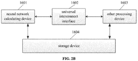
- the embodiments of the present application provide a combined processing device including the above-described neural network calculating device, a universal interconnection interface and other processing devices.
- FIG. 2A shows a schematic structural diagram of a combined processing apparatus according to embodiments of the present application.
- the combined processing device includes the above-described neural network calculating device 1601, universal interconnect interface 1602, and other processing devices 1603.
- the above other processing device 1603 includes a processor type of one or more of a general-purpose/dedicated processor such as a central processing unit, a graphics processing unit (GPU) and a neural network processor.
- a general-purpose/dedicated processor such as a central processing unit, a graphics processing unit (GPU) and a neural network processor.
- the number of processors included in the other processing device 1603 is not limited.
- the other processing device 1603 serving as an interface between the neural network calculating device 1601 and the external data and the control includes data moving, completing basic control such as starting and stopping of the neural network calculating device; the other processing device 1603 can also cooperate with the neural network calculating device 1601 to complete the operation task.
- the above universal interconnect interface 1602 is configured to transmit data and control instructions between the neural network calculating device 1601 and other processing devices 1603.
- the neural network calculating device 1601 obtains the required input data from other processing devices 1603 to write the storage device on the chip of the neural network calculating device 1601, acquire the control instruction from other processing device 1603 to write in the control buffer on the chip of the neural network calculating device 1601 and data in the storage device of the neural network calculating device 1601 can also be read to transmit to other processing devices 1603.
- the above combined processing device further includes a storage device 1604 configured to store data required by the present operation unit/operation device or other operation units and is particularly suitable for the data required to be calculated but cannot be completely stored in the internal memory of the present network operation device 1601 or other processing device 1603.
- a storage device 1604 configured to store data required by the present operation unit/operation device or other operation units and is particularly suitable for the data required to be calculated but cannot be completely stored in the internal memory of the present network operation device 1601 or other processing device 1603.
- the above combination device can be used as an on-chip system for smart devices such as mobile phones, robots, and drones, effectively reducing the core area of the control portion, increasing the processing speed and reducing the overall power consumption.
- the embodiments of the present application provide a neural network chip which includes the operation device described in any of the illustrated embodiments or the above-described neural network calculating device or the combined processing device.
- the embodiments of the present application provide a neural network chip package structure which includes the above neural network chip.
- the embodiments of the present application provide a board card which includes the above neural network chip package structure.
- the embodiments of the present application provide an electronic device including the above-mentioned board card.
- the electronic device includes a data processing device, a robot, a computer, a printer, a scanner, a tablet, a smart terminal, a mobile phone, a driving recorder, a navigator, a sensor, a camera, a cloud server, a camera, a camera, a projector, and a watch, headsets, a removable storage, a wearable device vehicle, a household appliance, and/or a medical device.
- the above-mentioned transportation includes airplanes, ships and/or vehicles;
- the above-mentioned household appliances include televisions, air conditioners, microwave ovens, refrigerators, rice cookers, humidifiers, washing machines, electric lights, gas stoves, range hoods;
- the medical equipment includes nuclear magnetic resonance instruments, B-mode ultrasound instrument and/or electrocardiograph.
- the embodiments of the present application further provide a computer storage medium, wherein the computer storage medium may store a program, and the program includes some or all of the steps of any one of the neural network operation methods according to the method embodiments.
- the computer storage medium may store a program
- the program includes some or all of the steps of any one of the neural network operation methods according to the method embodiments.
- the disclosed apparatus may be implemented in other ways.
- the device embodiments described above are merely illustrative, for example, the division of the unit is only a logical function division and there may be another division manner in the actual implementation, for example, multiple units or components may be combined or may be integrated into another system, or some features can be ignored or not performed.
- the mutual coupling or direct coupling or communication connection shown or discussed may be an indirect coupling or communication connection through some interfaces, devices or units, and may be electrical or other forms.
- the units described as separate components may or may not be physically separated, and the components displayed as units may or may not be physical units, that is, may be located in one place, or may be assigned to multiple network units. Some or all of the units may be selected according to actual needs to achieve the purpose of the solution of the embodiment.
- each functional unit in each embodiment of the present application may be integrated into one processing unit, or each unit may exist physically separately, or two or more units may be integrated into one unit.
- the above integrated unit can be implemented in the form of hardware or in the form of a software program module.
- the integrated unit if implemented in the form of a software program module and sold or used as a standalone product, may be stored in a computer readable memory.
- a computer readable memory A number of instructions are included to cause a computer device (which may be a personal computer, server or network device, etc.) to perform all or part of the steps of the methods described in various embodiments of the present application.
- the foregoing memory includes: a U disk, a Read-Only Memory (ROM), a Random Access Memory (RAM), a removable hard disk, a magnetic disk, or an optical disk, and the like which can store program codes.
Landscapes
- Engineering & Computer Science (AREA)
- Physics & Mathematics (AREA)
- Theoretical Computer Science (AREA)
- Software Systems (AREA)
- General Physics & Mathematics (AREA)
- General Engineering & Computer Science (AREA)
- Health & Medical Sciences (AREA)
- Life Sciences & Earth Sciences (AREA)
- Biomedical Technology (AREA)
- Biophysics (AREA)
- Mathematical Physics (AREA)
- Molecular Biology (AREA)
- General Health & Medical Sciences (AREA)
- Computing Systems (AREA)
- Evolutionary Computation (AREA)
- Data Mining & Analysis (AREA)
- Computational Linguistics (AREA)
- Artificial Intelligence (AREA)
- Neurology (AREA)
- Computational Mathematics (AREA)
- Mathematical Analysis (AREA)
- Mathematical Optimization (AREA)
- Pure & Applied Mathematics (AREA)
- Advance Control (AREA)
- Complex Calculations (AREA)
- Management, Administration, Business Operations System, And Electronic Commerce (AREA)
Priority Applications (1)
| Application Number | Priority Date | Filing Date | Title |
|---|---|---|---|
| EP19199531.5A EP3699826A1 (de) | 2017-04-20 | 2018-04-17 | Betriebsvorrichtung und zugehörige produkte |
Applications Claiming Priority (4)
| Application Number | Priority Date | Filing Date | Title |
|---|---|---|---|
| CN201710261742.3A CN108734279B (zh) | 2017-04-20 | 2017-04-20 | 一种运算装置和方法 |
| CN201710279834.4A CN108733352B (zh) | 2017-04-25 | 2017-04-25 | 支持向量排序的装置、方法及应用 |
| CN201710279655.0A CN108733739B (zh) | 2017-04-25 | 2017-04-25 | 支持集束搜索的运算装置和方法 |
| PCT/CN2018/083379 WO2018192492A1 (zh) | 2017-04-20 | 2018-04-17 | 一种运算装置及相关产品 |
Related Child Applications (2)
| Application Number | Title | Priority Date | Filing Date |
|---|---|---|---|
| EP19199531.5A Division-Into EP3699826A1 (de) | 2017-04-20 | 2018-04-17 | Betriebsvorrichtung und zugehörige produkte |
| EP19199531.5A Division EP3699826A1 (de) | 2017-04-20 | 2018-04-17 | Betriebsvorrichtung und zugehörige produkte |
Publications (3)
| Publication Number | Publication Date |
|---|---|
| EP3579152A1 true EP3579152A1 (de) | 2019-12-11 |
| EP3579152A4 EP3579152A4 (de) | 2020-04-22 |
| EP3579152B1 EP3579152B1 (de) | 2022-09-14 |
Family
ID=63856484
Family Applications (2)
| Application Number | Title | Priority Date | Filing Date |
|---|---|---|---|
| EP18787049.8A Active EP3579152B1 (de) | 2017-04-20 | 2018-04-17 | Rechenvorrichtung und zugehöriges produkt |
| EP19199531.5A Withdrawn EP3699826A1 (de) | 2017-04-20 | 2018-04-17 | Betriebsvorrichtung und zugehörige produkte |
Family Applications After (1)
| Application Number | Title | Priority Date | Filing Date |
|---|---|---|---|
| EP19199531.5A Withdrawn EP3699826A1 (de) | 2017-04-20 | 2018-04-17 | Betriebsvorrichtung und zugehörige produkte |
Country Status (4)
| Country | Link |
|---|---|
| US (1) | US11977968B2 (de) |
| EP (2) | EP3579152B1 (de) |
| CN (2) | CN109104876B (de) |
| WO (1) | WO2018192492A1 (de) |
Families Citing this family (34)
| Publication number | Priority date | Publication date | Assignee | Title |
|---|---|---|---|---|
| IL279363B2 (en) | 2018-06-21 | 2025-12-01 | Merck Sharp & Dohme | Pcsk9 antagonist compounds |
| CN111399905B (zh) * | 2019-01-02 | 2022-08-16 | 上海寒武纪信息科技有限公司 | 运算方法、装置及相关产品 |
| CN109754072B (zh) * | 2018-12-29 | 2020-06-23 | 中科寒武纪科技股份有限公司 | 网络离线模型的处理方法、人工智能处理装置及相关产品 |
| CN111488976B (zh) * | 2019-01-28 | 2023-06-30 | 中科寒武纪科技股份有限公司 | 神经网络计算装置、神经网络计算方法及相关产品 |
| CN111523656B (zh) * | 2019-02-03 | 2024-03-26 | 上海寒武纪信息科技有限公司 | 处理装置及方法 |
| CN111723921B (zh) * | 2019-03-22 | 2024-05-14 | 中科寒武纪科技股份有限公司 | 人工智能计算装置及相关产品 |
| CN111738429B (zh) * | 2019-03-25 | 2023-10-13 | 中科寒武纪科技股份有限公司 | 一种计算装置及相关产品 |
| CN109978160B (zh) * | 2019-03-25 | 2021-03-02 | 中科寒武纪科技股份有限公司 | 人工智能处理器的配置装置、方法及相关产品 |
| CN111831207B (zh) * | 2019-04-16 | 2024-06-11 | 阿里巴巴集团控股有限公司 | 一种数据处理方法、装置及其设备 |
| CN111915002B (zh) * | 2019-05-09 | 2023-12-19 | 中科寒武纪科技股份有限公司 | 运算方法、装置及相关产品 |
| CN111966325A (zh) * | 2019-05-20 | 2020-11-20 | 上海寒武纪信息科技有限公司 | 指令处理方法、装置及相关产品 |
| CN111966399B (zh) * | 2019-05-20 | 2024-06-07 | 上海寒武纪信息科技有限公司 | 指令处理方法、装置及相关产品 |
| CN111966400B (zh) * | 2019-05-20 | 2024-07-19 | 上海寒武纪信息科技有限公司 | 指令处理方法、装置及相关产品 |
| CN111966403A (zh) * | 2019-05-20 | 2020-11-20 | 上海寒武纪信息科技有限公司 | 指令处理方法、装置及相关产品 |
| CN110490315B (zh) * | 2019-08-14 | 2023-05-23 | 中科寒武纪科技股份有限公司 | 神经网络的反向运算稀疏方法及相关产品 |
| EP4076492A4 (de) | 2019-12-20 | 2024-01-17 | Merck Sharp & Dohme LLC | Pcsk9-antagonist-verbindungen |
| CN111126600A (zh) * | 2019-12-20 | 2020-05-08 | 上海寒武纪信息科技有限公司 | 神经网络模型的训练方法、数据处理方法和相关产品 |
| CN113032299B (zh) * | 2019-12-24 | 2023-09-26 | 中科寒武纪科技股份有限公司 | 用于处理请求的总线系统、集成电路装置、板卡及保序方法 |
| CN113032298B (zh) * | 2019-12-24 | 2023-09-29 | 中科寒武纪科技股份有限公司 | 用于保序的计算装置、集成电路装置、板卡及保序方法 |
| CN111260051B (zh) * | 2020-02-01 | 2024-05-14 | 上海寒武纪信息科技有限公司 | 神经网络运算方法及相关装置 |
| WO2021168644A1 (zh) * | 2020-02-25 | 2021-09-02 | 深圳市大疆创新科技有限公司 | 数据处理装置、电子设备和数据处理方法 |
| CN113626080B (zh) * | 2020-05-08 | 2023-10-03 | 安徽寒武纪信息科技有限公司 | 数据处理装置以及相关产品 |
| CN112152947B (zh) * | 2020-08-21 | 2021-07-20 | 北京百度网讯科技有限公司 | 处理器及实现方法、电子设备和存储介质 |
| CN114519167B (zh) * | 2020-11-19 | 2026-02-10 | 华为技术有限公司 | 一种算子计算方法、装置、设备及系统 |
| WO2022134873A1 (zh) * | 2020-12-25 | 2022-06-30 | 中科寒武纪科技股份有限公司 | 数据处理装置、数据处理方法及相关产品 |
| US12106206B2 (en) * | 2021-01-13 | 2024-10-01 | Apple Inc. | Multi-operational modes of neural engine circuit |
| CN112966182B (zh) * | 2021-03-09 | 2024-02-09 | 中国民航信息网络股份有限公司 | 一种项目推荐方法及相关设备 |
| CN112732433A (zh) * | 2021-03-30 | 2021-04-30 | 骊阳(广东)节能科技股份有限公司 | 一种可进行优先级调配的数据处理系统 |
| CN115185524B (zh) * | 2021-04-01 | 2026-04-28 | 广州希姆半导体科技有限公司 | 向量指令的识别方法、装置、电子设备及计算机可读存储介质 |
| CN112988238A (zh) * | 2021-05-06 | 2021-06-18 | 成都启英泰伦科技有限公司 | 一种基于可扩展指令集cpu内核的扩展运算装置及方法 |
| US20230110285A1 (en) * | 2021-10-13 | 2023-04-13 | Mellanox Technologies, Ltd. | Vector activation function to support machine learning inference and other processes |
| CN113920315B (zh) * | 2021-10-14 | 2024-04-30 | 江南大学 | 一种基于卷积神经网络的服装属性识别方法 |
| CN116402102A (zh) * | 2023-03-31 | 2023-07-07 | 北京奕斯伟计算技术股份有限公司 | 神经网络处理器和电子设备 |
| CN117807082B (zh) * | 2023-12-20 | 2024-09-27 | 中科驭数(北京)科技有限公司 | 哈希处理方法、装置、设备及计算机可读存储介质 |
Family Cites Families (16)
| Publication number | Priority date | Publication date | Assignee | Title |
|---|---|---|---|---|
| US5210870A (en) * | 1990-03-27 | 1993-05-11 | International Business Machines | Database sort and merge apparatus with multiple memory arrays having alternating access |
| DE19623033C1 (de) * | 1996-06-08 | 1997-10-16 | Aeg Electrocom Gmbh | Verfahren und Anordnung zur Mustererkennung auf statistischer Basis |
| GB2456775B (en) * | 2008-01-22 | 2012-10-31 | Advanced Risc Mach Ltd | Apparatus and method for performing permutation operations on data |
| US20120246533A1 (en) * | 2011-03-24 | 2012-09-27 | Sparsense, Inc. | Scalable hierarchical sparse representations supporting prediction, feedforward bottom-up estimation, and top-down influence for parallel and adaptive signal processing |
| EP2831691A4 (de) * | 2012-03-30 | 2015-11-25 | Intel Corp | Verfahren und vorrichtung für anweisungen zur zusammenführung und sortierung kleinerer sortierter vektoren zu einem grösseren sortierten vektor |
| CN102750131B (zh) * | 2012-06-07 | 2015-10-07 | 中国科学院计算机网络信息中心 | 一种面向gpu的双调归并排序方法 |
| US9977676B2 (en) * | 2013-11-15 | 2018-05-22 | Qualcomm Incorporated | Vector processing engines (VPEs) employing reordering circuitry in data flow paths between execution units and vector data memory to provide in-flight reordering of output vector data stored to vector data memory, and related vector processor systems and methods |
| US20150206050A1 (en) | 2014-01-23 | 2015-07-23 | Qualcomm Incorporated | Configuring neural network for low spiking rate |
| EP3274930A4 (de) | 2015-03-24 | 2018-11-21 | Hrl Laboratories, Llc | Module mit spärlicher inferenz zum tiefenlernen |
| US20160283864A1 (en) * | 2015-03-27 | 2016-09-29 | Qualcomm Incorporated | Sequential image sampling and storage of fine-tuned features |
| US10140572B2 (en) * | 2015-06-25 | 2018-11-27 | Microsoft Technology Licensing, Llc | Memory bandwidth management for deep learning applications |
| US11423323B2 (en) * | 2015-09-02 | 2022-08-23 | Qualcomm Incorporated | Generating a sparse feature vector for classification |
| CN105260776B (zh) * | 2015-09-10 | 2018-03-27 | 华为技术有限公司 | 神经网络处理器和卷积神经网络处理器 |
| CN106485315B (zh) * | 2015-10-08 | 2019-06-04 | 上海兆芯集成电路有限公司 | 具有输出缓冲器反馈与遮蔽功能的神经网络单元 |
| CN107545303B (zh) * | 2016-01-20 | 2021-09-07 | 中科寒武纪科技股份有限公司 | 用于稀疏人工神经网络的计算装置和运算方法 |
| CN106447034B (zh) | 2016-10-27 | 2019-07-30 | 中国科学院计算技术研究所 | 一种基于数据压缩的神经网络处理器、设计方法、芯片 |
-
2018
- 2018-04-17 WO PCT/CN2018/083379 patent/WO2018192492A1/zh not_active Ceased
- 2018-04-17 EP EP18787049.8A patent/EP3579152B1/de active Active
- 2018-04-17 US US16/476,261 patent/US11977968B2/en active Active
- 2018-04-17 CN CN201880000808.6A patent/CN109104876B/zh active Active
- 2018-04-17 CN CN201811011596.XA patent/CN109284823B/zh active Active
- 2018-04-17 EP EP19199531.5A patent/EP3699826A1/de not_active Withdrawn
Also Published As
| Publication number | Publication date |
|---|---|
| EP3579152B1 (de) | 2022-09-14 |
| US20200034698A1 (en) | 2020-01-30 |
| CN109284823A (zh) | 2019-01-29 |
| WO2018192492A1 (zh) | 2018-10-25 |
| EP3579152A4 (de) | 2020-04-22 |
| CN109104876A (zh) | 2018-12-28 |
| EP3699826A1 (de) | 2020-08-26 |
| CN109104876B (zh) | 2021-06-25 |
| US11977968B2 (en) | 2024-05-07 |
| CN109284823B (zh) | 2020-08-04 |
Similar Documents
| Publication | Publication Date | Title |
|---|---|---|
| EP3579152B1 (de) | Rechenvorrichtung und zugehöriges produkt | |
| US11983534B2 (en) | Calculation method and related product | |
| CN110163354B (zh) | 一种计算装置及方法 | |
| US11049002B2 (en) | Neural network computation device and method | |
| US10896369B2 (en) | Power conversion in neural networks | |
| CN110163334B (zh) | 集成电路芯片装置及相关产品 | |
| CN107992486A (zh) | 一种信息处理方法及相关产品 | |
| TW202321999A (zh) | 一種計算裝置及方法 | |
| CN111353591A (zh) | 一种计算装置及相关产品 | |
| CN110276447A (zh) | 一种计算装置及方法 | |
| CN111488963B (zh) | 神经网络计算装置和方法 | |
| CN113469365B (zh) | 基于神经网络模型的推理和编译方法及其相关产品 | |
| CN111930681B (zh) | 一种计算装置及相关产品 | |
| CN111047020A (zh) | 支持压缩及解压缩的神经网络运算装置及方法 | |
| CN111198714A (zh) | 重训练方法及相关产品 | |
| CN111260046B (zh) | 运算方法、装置及相关产品 | |
| CN111258641B (zh) | 运算方法、装置及相关产品 | |
| US10789531B2 (en) | Operation device and related products | |
| CN118278472A (zh) | 量化处理方法及相关装置 | |
| WO2019165939A1 (zh) | 一种计算装置及相关产品 |
Legal Events
| Date | Code | Title | Description |
|---|---|---|---|
| STAA | Information on the status of an ep patent application or granted ep patent |
Free format text: STATUS: THE INTERNATIONAL PUBLICATION HAS BEEN MADE |
|
| PUAI | Public reference made under article 153(3) epc to a published international application that has entered the european phase |
Free format text: ORIGINAL CODE: 0009012 |
|
| STAA | Information on the status of an ep patent application or granted ep patent |
Free format text: STATUS: REQUEST FOR EXAMINATION WAS MADE |
|
| 17P | Request for examination filed |
Effective date: 20181121 |
|
| AK | Designated contracting states |
Kind code of ref document: A1 Designated state(s): AL AT BE BG CH CY CZ DE DK EE ES FI FR GB GR HR HU IE IS IT LI LT LU LV MC MK MT NL NO PL PT RO RS SE SI SK SM TR |
|
| AX | Request for extension of the european patent |
Extension state: BA ME |
|
| A4 | Supplementary search report drawn up and despatched |
Effective date: 20200324 |
|
| RIC1 | Information provided on ipc code assigned before grant |
Ipc: G06F 9/30 20180101ALI20200318BHEP Ipc: G06N 3/08 20060101AFI20200318BHEP |
|
| STAA | Information on the status of an ep patent application or granted ep patent |
Free format text: STATUS: EXAMINATION IS IN PROGRESS |
|
| 17Q | First examination report despatched |
Effective date: 20200609 |
|
| DAV | Request for validation of the european patent (deleted) | ||
| DAX | Request for extension of the european patent (deleted) | ||
| GRAP | Despatch of communication of intention to grant a patent |
Free format text: ORIGINAL CODE: EPIDOSNIGR1 |
|
| STAA | Information on the status of an ep patent application or granted ep patent |
Free format text: STATUS: GRANT OF PATENT IS INTENDED |
|
| INTG | Intention to grant announced |
Effective date: 20220407 |
|
| GRAS | Grant fee paid |
Free format text: ORIGINAL CODE: EPIDOSNIGR3 |
|
| GRAA | (expected) grant |
Free format text: ORIGINAL CODE: 0009210 |
|
| STAA | Information on the status of an ep patent application or granted ep patent |
Free format text: STATUS: THE PATENT HAS BEEN GRANTED |
|
| AK | Designated contracting states |
Kind code of ref document: B1 Designated state(s): AL AT BE BG CH CY CZ DE DK EE ES FI FR GB GR HR HU IE IS IT LI LT LU LV MC MK MT NL NO PL PT RO RS SE SI SK SM TR |
|
| REG | Reference to a national code |
Ref country code: GB Ref legal event code: FG4D |
|
| REG | Reference to a national code |
Ref country code: CH Ref legal event code: EP |
|
| REG | Reference to a national code |
Ref country code: DE Ref legal event code: R096 Ref document number: 602018040698 Country of ref document: DE |
|
| REG | Reference to a national code |
Ref country code: IE Ref legal event code: FG4D |
|
| REG | Reference to a national code |
Ref country code: AT Ref legal event code: REF Ref document number: 1519180 Country of ref document: AT Kind code of ref document: T Effective date: 20221015 |
|
| REG | Reference to a national code |
Ref country code: LT Ref legal event code: MG9D |
|
| REG | Reference to a national code |
Ref country code: NL Ref legal event code: MP Effective date: 20220914 |
|
| PG25 | Lapsed in a contracting state [announced via postgrant information from national office to epo] |
Ref country code: SE Free format text: LAPSE BECAUSE OF FAILURE TO SUBMIT A TRANSLATION OF THE DESCRIPTION OR TO PAY THE FEE WITHIN THE PRESCRIBED TIME-LIMIT Effective date: 20220914 Ref country code: RS Free format text: LAPSE BECAUSE OF FAILURE TO SUBMIT A TRANSLATION OF THE DESCRIPTION OR TO PAY THE FEE WITHIN THE PRESCRIBED TIME-LIMIT Effective date: 20220914 Ref country code: NO Free format text: LAPSE BECAUSE OF FAILURE TO SUBMIT A TRANSLATION OF THE DESCRIPTION OR TO PAY THE FEE WITHIN THE PRESCRIBED TIME-LIMIT Effective date: 20221214 Ref country code: LV Free format text: LAPSE BECAUSE OF FAILURE TO SUBMIT A TRANSLATION OF THE DESCRIPTION OR TO PAY THE FEE WITHIN THE PRESCRIBED TIME-LIMIT Effective date: 20220914 Ref country code: LT Free format text: LAPSE BECAUSE OF FAILURE TO SUBMIT A TRANSLATION OF THE DESCRIPTION OR TO PAY THE FEE WITHIN THE PRESCRIBED TIME-LIMIT Effective date: 20220914 Ref country code: FI Free format text: LAPSE BECAUSE OF FAILURE TO SUBMIT A TRANSLATION OF THE DESCRIPTION OR TO PAY THE FEE WITHIN THE PRESCRIBED TIME-LIMIT Effective date: 20220914 |
|
| REG | Reference to a national code |
Ref country code: AT Ref legal event code: MK05 Ref document number: 1519180 Country of ref document: AT Kind code of ref document: T Effective date: 20220914 |
|
| PG25 | Lapsed in a contracting state [announced via postgrant information from national office to epo] |
Ref country code: HR Free format text: LAPSE BECAUSE OF FAILURE TO SUBMIT A TRANSLATION OF THE DESCRIPTION OR TO PAY THE FEE WITHIN THE PRESCRIBED TIME-LIMIT Effective date: 20220914 Ref country code: GR Free format text: LAPSE BECAUSE OF FAILURE TO SUBMIT A TRANSLATION OF THE DESCRIPTION OR TO PAY THE FEE WITHIN THE PRESCRIBED TIME-LIMIT Effective date: 20221215 |
|
| PG25 | Lapsed in a contracting state [announced via postgrant information from national office to epo] |
Ref country code: SM Free format text: LAPSE BECAUSE OF FAILURE TO SUBMIT A TRANSLATION OF THE DESCRIPTION OR TO PAY THE FEE WITHIN THE PRESCRIBED TIME-LIMIT Effective date: 20220914 Ref country code: RO Free format text: LAPSE BECAUSE OF FAILURE TO SUBMIT A TRANSLATION OF THE DESCRIPTION OR TO PAY THE FEE WITHIN THE PRESCRIBED TIME-LIMIT Effective date: 20220914 Ref country code: PT Free format text: LAPSE BECAUSE OF FAILURE TO SUBMIT A TRANSLATION OF THE DESCRIPTION OR TO PAY THE FEE WITHIN THE PRESCRIBED TIME-LIMIT Effective date: 20230116 Ref country code: ES Free format text: LAPSE BECAUSE OF FAILURE TO SUBMIT A TRANSLATION OF THE DESCRIPTION OR TO PAY THE FEE WITHIN THE PRESCRIBED TIME-LIMIT Effective date: 20220914 Ref country code: CZ Free format text: LAPSE BECAUSE OF FAILURE TO SUBMIT A TRANSLATION OF THE DESCRIPTION OR TO PAY THE FEE WITHIN THE PRESCRIBED TIME-LIMIT Effective date: 20220914 Ref country code: AT Free format text: LAPSE BECAUSE OF FAILURE TO SUBMIT A TRANSLATION OF THE DESCRIPTION OR TO PAY THE FEE WITHIN THE PRESCRIBED TIME-LIMIT Effective date: 20220914 |
|
| PG25 | Lapsed in a contracting state [announced via postgrant information from national office to epo] |
Ref country code: SK Free format text: LAPSE BECAUSE OF FAILURE TO SUBMIT A TRANSLATION OF THE DESCRIPTION OR TO PAY THE FEE WITHIN THE PRESCRIBED TIME-LIMIT Effective date: 20220914 Ref country code: PL Free format text: LAPSE BECAUSE OF FAILURE TO SUBMIT A TRANSLATION OF THE DESCRIPTION OR TO PAY THE FEE WITHIN THE PRESCRIBED TIME-LIMIT Effective date: 20220914 Ref country code: IS Free format text: LAPSE BECAUSE OF FAILURE TO SUBMIT A TRANSLATION OF THE DESCRIPTION OR TO PAY THE FEE WITHIN THE PRESCRIBED TIME-LIMIT Effective date: 20230114 Ref country code: EE Free format text: LAPSE BECAUSE OF FAILURE TO SUBMIT A TRANSLATION OF THE DESCRIPTION OR TO PAY THE FEE WITHIN THE PRESCRIBED TIME-LIMIT Effective date: 20220914 |
|
| REG | Reference to a national code |
Ref country code: DE Ref legal event code: R097 Ref document number: 602018040698 Country of ref document: DE |
|
| PG25 | Lapsed in a contracting state [announced via postgrant information from national office to epo] |
Ref country code: NL Free format text: LAPSE BECAUSE OF FAILURE TO SUBMIT A TRANSLATION OF THE DESCRIPTION OR TO PAY THE FEE WITHIN THE PRESCRIBED TIME-LIMIT Effective date: 20220914 Ref country code: AL Free format text: LAPSE BECAUSE OF FAILURE TO SUBMIT A TRANSLATION OF THE DESCRIPTION OR TO PAY THE FEE WITHIN THE PRESCRIBED TIME-LIMIT Effective date: 20220914 |
|
| PLBE | No opposition filed within time limit |
Free format text: ORIGINAL CODE: 0009261 |
|
| STAA | Information on the status of an ep patent application or granted ep patent |
Free format text: STATUS: NO OPPOSITION FILED WITHIN TIME LIMIT |
|
| PG25 | Lapsed in a contracting state [announced via postgrant information from national office to epo] |
Ref country code: DK Free format text: LAPSE BECAUSE OF FAILURE TO SUBMIT A TRANSLATION OF THE DESCRIPTION OR TO PAY THE FEE WITHIN THE PRESCRIBED TIME-LIMIT Effective date: 20220914 |
|
| 26N | No opposition filed |
Effective date: 20230615 |
|
| PG25 | Lapsed in a contracting state [announced via postgrant information from national office to epo] |
Ref country code: SI Free format text: LAPSE BECAUSE OF FAILURE TO SUBMIT A TRANSLATION OF THE DESCRIPTION OR TO PAY THE FEE WITHIN THE PRESCRIBED TIME-LIMIT Effective date: 20220914 |
|
| REG | Reference to a national code |
Ref country code: CH Ref legal event code: PL |
|
| PG25 | Lapsed in a contracting state [announced via postgrant information from national office to epo] |
Ref country code: LU Free format text: LAPSE BECAUSE OF NON-PAYMENT OF DUE FEES Effective date: 20230417 |
|
| REG | Reference to a national code |
Ref country code: BE Ref legal event code: MM Effective date: 20230430 |
|
| PG25 | Lapsed in a contracting state [announced via postgrant information from national office to epo] |
Ref country code: MC Free format text: LAPSE BECAUSE OF FAILURE TO SUBMIT A TRANSLATION OF THE DESCRIPTION OR TO PAY THE FEE WITHIN THE PRESCRIBED TIME-LIMIT Effective date: 20220914 |
|
| PG25 | Lapsed in a contracting state [announced via postgrant information from national office to epo] |
Ref country code: MC Free format text: LAPSE BECAUSE OF FAILURE TO SUBMIT A TRANSLATION OF THE DESCRIPTION OR TO PAY THE FEE WITHIN THE PRESCRIBED TIME-LIMIT Effective date: 20220914 Ref country code: LI Free format text: LAPSE BECAUSE OF NON-PAYMENT OF DUE FEES Effective date: 20230430 Ref country code: CH Free format text: LAPSE BECAUSE OF NON-PAYMENT OF DUE FEES Effective date: 20230430 |
|
| REG | Reference to a national code |
Ref country code: IE Ref legal event code: MM4A |
|
| PG25 | Lapsed in a contracting state [announced via postgrant information from national office to epo] |
Ref country code: BE Free format text: LAPSE BECAUSE OF NON-PAYMENT OF DUE FEES Effective date: 20230430 |
|
| PG25 | Lapsed in a contracting state [announced via postgrant information from national office to epo] |
Ref country code: IE Free format text: LAPSE BECAUSE OF NON-PAYMENT OF DUE FEES Effective date: 20230417 |
|
| PG25 | Lapsed in a contracting state [announced via postgrant information from national office to epo] |
Ref country code: IE Free format text: LAPSE BECAUSE OF NON-PAYMENT OF DUE FEES Effective date: 20230417 |
|
| PG25 | Lapsed in a contracting state [announced via postgrant information from national office to epo] |
Ref country code: IT Free format text: LAPSE BECAUSE OF FAILURE TO SUBMIT A TRANSLATION OF THE DESCRIPTION OR TO PAY THE FEE WITHIN THE PRESCRIBED TIME-LIMIT Effective date: 20220914 |
|
| PG25 | Lapsed in a contracting state [announced via postgrant information from national office to epo] |
Ref country code: BG Free format text: LAPSE BECAUSE OF FAILURE TO SUBMIT A TRANSLATION OF THE DESCRIPTION OR TO PAY THE FEE WITHIN THE PRESCRIBED TIME-LIMIT Effective date: 20220914 |
|
| PG25 | Lapsed in a contracting state [announced via postgrant information from national office to epo] |
Ref country code: BG Free format text: LAPSE BECAUSE OF FAILURE TO SUBMIT A TRANSLATION OF THE DESCRIPTION OR TO PAY THE FEE WITHIN THE PRESCRIBED TIME-LIMIT Effective date: 20220914 |
|
| PGFP | Annual fee paid to national office [announced via postgrant information from national office to epo] |
Ref country code: DE Payment date: 20250422 Year of fee payment: 8 |
|
| PGFP | Annual fee paid to national office [announced via postgrant information from national office to epo] |
Ref country code: FR Payment date: 20250425 Year of fee payment: 8 |
|
| PG25 | Lapsed in a contracting state [announced via postgrant information from national office to epo] |
Ref country code: CY Free format text: LAPSE BECAUSE OF FAILURE TO SUBMIT A TRANSLATION OF THE DESCRIPTION OR TO PAY THE FEE WITHIN THE PRESCRIBED TIME-LIMIT; INVALID AB INITIO Effective date: 20180417 |
|
| PG25 | Lapsed in a contracting state [announced via postgrant information from national office to epo] |
Ref country code: HU Free format text: LAPSE BECAUSE OF FAILURE TO SUBMIT A TRANSLATION OF THE DESCRIPTION OR TO PAY THE FEE WITHIN THE PRESCRIBED TIME-LIMIT; INVALID AB INITIO Effective date: 20180417 |
|
| PG25 | Lapsed in a contracting state [announced via postgrant information from national office to epo] |
Ref country code: TR Free format text: LAPSE BECAUSE OF FAILURE TO SUBMIT A TRANSLATION OF THE DESCRIPTION OR TO PAY THE FEE WITHIN THE PRESCRIBED TIME-LIMIT Effective date: 20220914 |
|
| PGFP | Annual fee paid to national office [announced via postgrant information from national office to epo] |
Ref country code: GB Payment date: 20260313 Year of fee payment: 9 |