EP3579234A1 - Hochgenaue niederleistungs-stromreferenz für stark verteilte stromreferenzen für einen kreuzungspunktspeicher - Google Patents
Hochgenaue niederleistungs-stromreferenz für stark verteilte stromreferenzen für einen kreuzungspunktspeicher Download PDFInfo
- Publication number
- EP3579234A1 EP3579234A1 EP19188039.2A EP19188039A EP3579234A1 EP 3579234 A1 EP3579234 A1 EP 3579234A1 EP 19188039 A EP19188039 A EP 19188039A EP 3579234 A1 EP3579234 A1 EP 3579234A1
- Authority
- EP
- European Patent Office
- Prior art keywords
- current
- terminal
- coupled
- output
- active device
- Prior art date
- Legal status (The legal status is an assumption and is not a legal conclusion. Google has not performed a legal analysis and makes no representation as to the accuracy of the status listed.)
- Granted
Links
Images


Classifications
-
- G—PHYSICS
- G11—INFORMATION STORAGE
- G11C—STATIC STORES
- G11C5/00—Details of stores covered by group G11C11/00
- G11C5/14—Power supply arrangements, e.g. power down, chip selection or deselection, layout of wirings or power grids, or multiple supply levels
-
- G—PHYSICS
- G11—INFORMATION STORAGE
- G11C—STATIC STORES
- G11C5/00—Details of stores covered by group G11C11/00
- G11C5/14—Power supply arrangements, e.g. power down, chip selection or deselection, layout of wirings or power grids, or multiple supply levels
- G11C5/147—Voltage reference generators, voltage or current regulators; Internally lowered supply levels; Compensation for voltage drops
-
- G—PHYSICS
- G05—CONTROLLING; REGULATING
- G05F—SYSTEMS FOR REGULATING ELECTRIC OR MAGNETIC VARIABLES
- G05F3/00—Non-retroactive systems for regulating electric variables by using an uncontrolled element, or an uncontrolled combination of elements, such element or such combination having self-regulating properties
- G05F3/02—Regulating voltage or current
- G05F3/08—Regulating voltage or current wherein the variable is DC
-
- G—PHYSICS
- G05—CONTROLLING; REGULATING
- G05F—SYSTEMS FOR REGULATING ELECTRIC OR MAGNETIC VARIABLES
- G05F3/00—Non-retroactive systems for regulating electric variables by using an uncontrolled element, or an uncontrolled combination of elements, such element or such combination having self-regulating properties
- G05F3/02—Regulating voltage or current
- G05F3/08—Regulating voltage or current wherein the variable is DC
- G05F3/10—Regulating voltage or current wherein the variable is DC using uncontrolled devices with non-linear characteristics
- G05F3/16—Regulating voltage or current wherein the variable is DC using uncontrolled devices with non-linear characteristics being semiconductor devices
- G05F3/20—Regulating voltage or current wherein the variable is DC using uncontrolled devices with non-linear characteristics being semiconductor devices using diode- transistor combinations
- G05F3/26—Current mirrors
-
- G—PHYSICS
- G11—INFORMATION STORAGE
- G11C—STATIC STORES
- G11C27/00—Electric analogue stores, e.g. for storing instantaneous values
- G11C27/02—Sample-and-hold arrangements
-
- G—PHYSICS
- G11—INFORMATION STORAGE
- G11C—STATIC STORES
- G11C27/00—Electric analogue stores, e.g. for storing instantaneous values
- G11C27/02—Sample-and-hold arrangements
- G11C27/024—Sample-and-hold arrangements using a capacitive memory element
-
- G—PHYSICS
- G11—INFORMATION STORAGE
- G11C—STATIC STORES
- G11C7/00—Arrangements for writing information into, or reading information out from, a digital store
- G11C7/10—Input/output [I/O] data interface arrangements, e.g. I/O data control circuits, I/O data buffers
-
- G—PHYSICS
- G11—INFORMATION STORAGE
- G11C—STATIC STORES
- G11C7/00—Arrangements for writing information into, or reading information out from, a digital store
- G11C7/14—Dummy cell management; Sense reference voltage generators
Definitions
- the subject matter disclosed herein relates to cross-point memories. More particularly, the subject matter disclosed herein relates to a low-power, high-accuracy current reference for highly distributed current reference for a solid-state memory, such as a cross-point memory.
- a three-dimensional (3D) cross-point memory is a solid-state, non-volatile type of memory that for some memory operations requires delivery of accurate currents at many locations around a cross-point memory chip.
- 3D three-dimensional
- a cross-point memory chip over 8000 locations on the chip require an accurate low-power current reference that can instantaneously deliver a reference current for a memory operation. Transferring a reference current from a central location to each of a plurality of current mirrors that are highly distributed across a chip has serious drawbacks in both power and chip-area use considerations.
- Another approach that has been used is to transfer a bias voltage that is remotely converted into a reference current at a plurality of locations.
- each separate current reference source must be calibrated to remove mismatches, such as random device offsets that can appear around a chip that are caused by process offsets. Additionally, the remotely generated reference current is sensitive to bias voltage noise, temperature variations, and supply voltage variations.
- the subject matter disclosed herein relates to cross-point memories. More particularly, the subject matter disclosed herein relates to a low-power, high-accuracy current reference for highly distributed current reference for a cross-point memory.
- numerous specific details are set forth to provide a thorough understanding of embodiments disclosed herein.
- One skilled in the relevant art will recognize, however, that the embodiments disclosed herein can be practiced without one or more of the specific details, or with other methods, components, materials, and so forth. In other instances, well-known structures, materials, or operations are not shown or described in detail to avoid obscuring aspects of the specification.
- the subject matter disclosed herein provides a low-power, high-accuracy current reference system that can be used for highly distributed current references of a solid-state memory, such as, but not limited to, a cross-point memory.
- the low-power, high-accuracy current reference system disclosed herein comprises part of a solid-state drive.
- Embodiments of the subject matter disclosed herein utilize a source degeneration technique to compensate for current, temperature, supply and process variations. That is, embodiment of the subject matter disclosed herein use an active Metal-Oxide Semiconductor (MOS) device as a source degeneration resistance with active biasing that significantly reduces adverse influences of bias voltage noise, supply voltage variations and device offsets.
- MOS Metal-Oxide Semiconductor
- embodiments of the subject matter disclosed herein provide a particularly low-power current reference system that is instantly available even during an exit from a standby mode by remaining in a sample-and-hold mode for long periods of time. Moreover, embodiments of the subject matter disclosed herein use a relatively small area in comparison to conventional techniques. Although the subject matter disclosed herein is described in relationship to a cross-point memory, a solid-state memory and/or a solid-state drive, it should be understood that the subject matter disclosed herein is not so limited and is applicable in a system that utilizes highly distributed current references, such as, but not limited to, imaging systems and other sensor systems.
- FIG. 1 depicts a schematic diagram of a first exemplary embodiment of a highly distributed current reference 100 according to the subject matter disclosed herein.
- Highly distributed current reference 100 comprises a centrally located current digital-to-analog converter (IDAC) 101 and a plurality of remotely located TILE current references 102, of which only one remotely located TILE current reference 102 is shown.
- IDAC 101 comprises a first current source IBIAS/N, a second current source IBIAS, three Complementary Metal Oxide Semiconductor (CMOS) active devices M1-M3, a first buffer amplifier 110, a second buffer amplifier 111, and first and second switches 112 and 113.
- CMOS Complementary Metal Oxide Semiconductor
- One terminal of current source IBIAS/N is coupled to a power supply voltage Vcc and the other terminal of current source IBIAS/N is coupled to the drain and the gate of active device M1.
- the source of active device M1 is coupled to a supply voltage HNVNN.
- One terminal of current source IBIAS is coupled to power supply voltage Vcc and the other terminal of current source IBIAS is coupled to the drain and the gate of active device M2.
- the source of active device M2 is coupled to the drain of active device M3.
- the gate of active device M3 is coupled to the drain and gate of active device M1.
- the source of active device M3 is coupled to supply voltage HNVNN.
- the drain of active device M2 is coupled to the input to buffer amplifier 110, and the gate of active device M3 is coupled to the input of buffer amplifier 111.
- the output of buffer amplifier 110 is coupled to the input of switch 112, and the output of buffer amplifier 111 is coupled to the input of switch 113.
- the output of switch 112 is coupled to a signal line SETBIAS.
- the output of switch 113 is coupled to signal line RESBIAS.
- the voltages appearing on the SETBIAS and RESBIAS signal lines are respectively based on a magnitude of the current through current source IBIAS and a magnitude of the current through current source IBIAS/N.
- Buffer amplifiers 110 and 111 have sufficient drive capability to charge capacitances C1 and C2, which respectively represent the coupling capacitance between signal line SETBIAS and supply voltage HNVNN and between signal line RESBIAS and supply voltage HNVNN.
- Switches 112 and 113 are each controlled to sample and hold the respective outputs of buffer amplifiers 110 and 111 by a SAMPLE_EN signal.
- the circuitry of IDAC 101 is capable of being turned off (i.e., placed in a standby mode), and when the voltages on signal lines SETBIAS and RESBIAS are to be refreshed, the circuitry of IDAC 101 is powered up and allowed to stabilize to refresh the voltages on signal lines SETBIAS and RESBIAS.
- SAMPLE_EN is then controlled to be "true” so that switches 112 and 113 are actuated and signal lines SETBIAS and RESBIAS are refreshed.
- SAMPLE_EN is then controlled to be "not true,” thereby opening switches 112 and 113.
- the circuitry of IDAC 101 is then controlled to be turned off (i.e., the standby mode) so that the highly distributed current reference does not dissipate power during the time that signal lines SETBIAS and RESBIAS are not being refreshed.
- Signals lines SETBIAS and RESBIAS are distributed around the integrated circuit to a plurality of TILE current references 102, of which only one is shown in Figure 1 .
- signal lines SETBIAS and RESBIAS are coupled to more than 8000 TILE current references 102.
- each TILE current reference 102 comprises CMOS active devices M4 and M5.
- the drain of active device M4 is coupled to a supply voltage HNREG, and the source of active device M4 is coupled to the drain of active device M5.
- the source of active device M5 is coupled to supply voltage HNVNN.
- the gate of active device M4 is coupled to signal line SETBIAS, and the gate of active device M5 is coupled to signal line RESBIAS.
- node HNREG comprises a node through which current passing through active device M4 is controlled by IDAC 101.
- the voltage drop across the degeneration resistance e.g., about 500 mV
- HNVNN V t mismatch or supply variation
- the SETBIAS and RESBIAS signal lines track sudden HNVNN voltage variations based on the capacitance between them (i.e., capacitors C1 and C2).
- signal lines SETBIAS and RESBIAS and power supply HNVNN are physically arranged to remain in close proximity to each other as they are distributed around an integrated circuit. That is, the capacitance C1 between the SETBIAS line and power supply HNVNN and the capacitance C2 between the RESBIAS line and power supply HNVNN reduce inaccuracies caused by power supply variations coupling through active devices M4 and M5, and holds the bias for long periods of time (allowing for a sample-to-hold ratio in excess of 1:1000), thereby significantly reducing power consumption.
- capacitors C1 and C2 are depicted in the Figures using dashed lines because both C1 and C2 are distributed capacitances instead of being lumped-value capacitances. It should also be understood that in an alternative exemplary embodiment, at least a portion of capacitor C1 and/or C2 could comprise a lumped-value capacitance.
- FIG 2 depicts a schematic diagram of a second exemplary embodiment of a highly distributed current reference 200 according to the subject matter disclosed herein.
- the circuit configuration of highly distributed current reference 200 is similar to highly distributed current reference 100 ( Figure 1 ) except that active device M3 of IDAC 201 is coupled to a supply voltage VI and no RESBIAS signal line is used. Supply voltage VI can be an available supply voltage.
- Supply voltage VI can be an available supply voltage.
- IBIAS/N and active device M1 are not needed for IDAC 201.
- Signal line SETBIAS for distributed current reference 200 is distributed around an integrated circuit to a plurality of TILE current references 102, of which only one is shown in Figure 2 .
- Tile current references 102 are configured similar to the tile current references depicted in Figure 1 .
- FIG 3 depicts a schematic diagram of a third exemplary embodiment of a highly distributed current reference 300 according to the subject matter disclosed herein.
- the circuit configuration of highly distributed current reference 300 is similar to highly distributed current reference 200 ( Figure 2 ) except that device M3 of IDAC 301 is embodied as a resistance R1 instead of an active device.
- a TILE current reference 302 is similar to TILE current reference 102 except active device M5 is embodied as a resistance R2 having a resistance value equal to or about equal to the resistance value of resistance R1.
- active devices M3 and M5 in Figure 1 could each be replaced with a degenerative resistance. It should be understood that devices M3 and M5 for any of the exemplary embodiments disclosed herein could be metal oxide semiconductor (MOS) devices, resistances, or a combination thereof.
- MOS metal oxide semiconductor
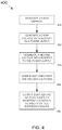
- Figure 4 depicts an exemplary embodiment of a process 400 for generating a reference current according to the subject matter disclosed herein.
- a first current is generated, such as IBIAS in Figure 1 .
- a first voltage signal is generated based with respect to a first power supply.
- the first voltage signal in some exemplary embodiments may correspond to the voltage at the output from buffer 110 in Figure 1 , which is generated with respect to power supply HNVNN.
- a second voltage is generated with respect to the first power supply.
- the second voltage signal is some exemplary embodiments may correspond to the voltage at the output of buffer 111 in Figure 1 , which is generated with respect to power supply HNVNN.
- the first and second voltages are respectively sampled and held.
- the held first and second voltages are output to a plurality of remotely located tile current device, such as a tile current 102 in Figure 1 .
- the first voltage signal and the second voltage signal are generated using a degeneration-resistance device, which could comprise a metal oxide semiconductor (MOS) device or a resistance.
- MOS metal oxide semiconductor
Landscapes
- Engineering & Computer Science (AREA)
- Physics & Mathematics (AREA)
- Automation & Control Theory (AREA)
- Electromagnetism (AREA)
- General Physics & Mathematics (AREA)
- Radar, Positioning & Navigation (AREA)
- Power Engineering (AREA)
- Microelectronics & Electronic Packaging (AREA)
- Nonlinear Science (AREA)
- Control Of Electrical Variables (AREA)
- Static Random-Access Memory (AREA)
- Read Only Memory (AREA)
- Semiconductor Integrated Circuits (AREA)
Applications Claiming Priority (3)
| Application Number | Priority Date | Filing Date | Title |
|---|---|---|---|
| US13/853,813 US9280168B2 (en) | 2013-03-29 | 2013-03-29 | Low-power, high-accuracy current reference for highly distributed current references for cross point memory |
| EP14774639.0A EP2979268B1 (de) | 2013-03-29 | 2014-02-13 | Hochgenaue niederleistungs-stromreferenz für stark verteilte stromreferenzen für einen kreuzungspunktspeicher |
| PCT/US2014/016288 WO2014158414A1 (en) | 2013-03-29 | 2014-02-13 | Low-power, high-accuracy current reference for highly distributed current references for cross point memory |
Related Parent Applications (2)
| Application Number | Title | Priority Date | Filing Date |
|---|---|---|---|
| EP14774639.0A Division-Into EP2979268B1 (de) | 2013-03-29 | 2014-02-13 | Hochgenaue niederleistungs-stromreferenz für stark verteilte stromreferenzen für einen kreuzungspunktspeicher |
| EP14774639.0A Division EP2979268B1 (de) | 2013-03-29 | 2014-02-13 | Hochgenaue niederleistungs-stromreferenz für stark verteilte stromreferenzen für einen kreuzungspunktspeicher |
Publications (2)
| Publication Number | Publication Date |
|---|---|
| EP3579234A1 true EP3579234A1 (de) | 2019-12-11 |
| EP3579234B1 EP3579234B1 (de) | 2021-03-31 |
Family
ID=51620730
Family Applications (2)
| Application Number | Title | Priority Date | Filing Date |
|---|---|---|---|
| EP14774639.0A Active EP2979268B1 (de) | 2013-03-29 | 2014-02-13 | Hochgenaue niederleistungs-stromreferenz für stark verteilte stromreferenzen für einen kreuzungspunktspeicher |
| EP19188039.2A Active EP3579234B1 (de) | 2013-03-29 | 2014-02-13 | Hochgenaue niederleistungs-stromreferenz für stark verteilte stromreferenzen für einen kreuzungspunktspeicher |
Family Applications Before (1)
| Application Number | Title | Priority Date | Filing Date |
|---|---|---|---|
| EP14774639.0A Active EP2979268B1 (de) | 2013-03-29 | 2014-02-13 | Hochgenaue niederleistungs-stromreferenz für stark verteilte stromreferenzen für einen kreuzungspunktspeicher |
Country Status (6)
| Country | Link |
|---|---|
| US (3) | US9280168B2 (de) |
| EP (2) | EP2979268B1 (de) |
| JP (1) | JP6228662B2 (de) |
| KR (2) | KR101692924B1 (de) |
| CN (1) | CN105027209B (de) |
| WO (1) | WO2014158414A1 (de) |
Families Citing this family (10)
| Publication number | Priority date | Publication date | Assignee | Title |
|---|---|---|---|---|
| US9280168B2 (en) * | 2013-03-29 | 2016-03-08 | Intel Corporation | Low-power, high-accuracy current reference for highly distributed current references for cross point memory |
| US9672930B2 (en) * | 2015-05-29 | 2017-06-06 | Silicon Storage Technology, Inc. | Low power operation for flash memory system |
| US10242750B2 (en) * | 2017-05-31 | 2019-03-26 | Sandisk Technologies Llc | High-speed data path testing techniques for non-volatile memory |
| JP6501325B1 (ja) * | 2018-01-30 | 2019-04-17 | ウィンボンド エレクトロニクス コーポレーション | 半導体記憶装置 |
| KR102487550B1 (ko) | 2018-06-29 | 2023-01-11 | 삼성전자주식회사 | 메모리 장치 및 그 동작 방법 |
| KR102661099B1 (ko) | 2018-11-08 | 2024-04-29 | 삼성전자주식회사 | 전송 소자를 포함하는 불휘발성 메모리 장치 |
| CN109671460B (zh) * | 2018-12-17 | 2020-08-25 | 上海贝岭股份有限公司 | 用于读写操作的缓存电路和存储器 |
| KR102710370B1 (ko) | 2019-10-01 | 2024-09-26 | 삼성전자주식회사 | 저항성 메모리 장치 및 저항성 메모리 장치의 동작 방법 |
| US11521693B2 (en) | 2021-02-05 | 2022-12-06 | Nxp B.V. | Sample and hold circuit for current |
| CN118191391B (zh) * | 2022-12-14 | 2026-02-27 | 上海韦尔半导体股份有限公司 | 输出检测电路 |
Citations (4)
| Publication number | Priority date | Publication date | Assignee | Title |
|---|---|---|---|---|
| US20060066360A1 (en) * | 2004-09-29 | 2006-03-30 | Via Technologies, Inc. | Switched operation amplifier |
| US20090085654A1 (en) * | 2007-09-29 | 2009-04-02 | Yung-Cheng Lin | Biasing Circuit with Fast Response |
| US20110188283A1 (en) * | 2010-02-01 | 2011-08-04 | Unity Semiconductor Corporation | Circuits and techniques to compensate data signals for variations of parameters affecting memory cells in cross-point arrays |
| US20110215837A1 (en) * | 2010-03-03 | 2011-09-08 | Macronix International Co., Ltd. | Clock generator circuits for generating clock signals |
Family Cites Families (12)
| Publication number | Priority date | Publication date | Assignee | Title |
|---|---|---|---|---|
| JP3803107B2 (ja) * | 1994-08-04 | 2006-08-02 | 株式会社ルネサステクノロジ | 半導体装置および電源電圧発生回路 |
| US6724662B2 (en) * | 2002-09-04 | 2004-04-20 | Atmel Corporation | Method of recovering overerased bits in a memory device |
| JP4623936B2 (ja) * | 2003-01-09 | 2011-02-02 | 株式会社デンソー | 遠隔にある複数負荷への定電流供給回路 |
| US7023753B2 (en) | 2003-11-30 | 2006-04-04 | Union Semiconductor Technology Corporation | Current controlled word and sense source |
| US7227804B1 (en) | 2004-04-19 | 2007-06-05 | Cypress Semiconductor Corporation | Current source architecture for memory device standby current reduction |
| US7944281B2 (en) | 2008-12-12 | 2011-05-17 | Mosys, Inc. | Constant reference cell current generator for non-volatile memories |
| KR101532268B1 (ko) * | 2008-12-18 | 2015-07-01 | 삼성전자주식회사 | 디지털-아날로그 변환기, 이를 포함하는 소스 구동회로, 및소스 구동회로를 포함하는 표시 장치 |
| JP2012004627A (ja) * | 2010-06-14 | 2012-01-05 | Toshiba Corp | カレントミラー回路 |
| US8729883B2 (en) | 2011-06-29 | 2014-05-20 | Synopsys, Inc. | Current source with low power consumption and reduced on-chip area occupancy |
| US9019005B2 (en) * | 2012-06-28 | 2015-04-28 | Infineon Technologies Ag | Voltage regulating circuit |
| US9280168B2 (en) * | 2013-03-29 | 2016-03-08 | Intel Corporation | Low-power, high-accuracy current reference for highly distributed current references for cross point memory |
| KR102204678B1 (ko) * | 2014-12-11 | 2021-01-20 | 삼성전자주식회사 | 인버터 증폭기 기반의 이중 루프 레귤레이터 및 그에 따른 전압 레귤레이팅 방법 |
-
2013
- 2013-03-29 US US13/853,813 patent/US9280168B2/en active Active
-
2014
- 2014-02-13 KR KR1020157022388A patent/KR101692924B1/ko active Active
- 2014-02-13 CN CN201480011139.4A patent/CN105027209B/zh active Active
- 2014-02-13 EP EP14774639.0A patent/EP2979268B1/de active Active
- 2014-02-13 WO PCT/US2014/016288 patent/WO2014158414A1/en not_active Ceased
- 2014-02-13 KR KR1020167036897A patent/KR101813833B1/ko active Active
- 2014-02-13 JP JP2016505462A patent/JP6228662B2/ja active Active
- 2014-02-13 EP EP19188039.2A patent/EP3579234B1/de active Active
-
2016
- 2016-01-25 US US15/005,194 patent/US9997207B2/en active Active
-
2018
- 2018-06-06 US US16/001,396 patent/US10553257B2/en active Active
Patent Citations (4)
| Publication number | Priority date | Publication date | Assignee | Title |
|---|---|---|---|---|
| US20060066360A1 (en) * | 2004-09-29 | 2006-03-30 | Via Technologies, Inc. | Switched operation amplifier |
| US20090085654A1 (en) * | 2007-09-29 | 2009-04-02 | Yung-Cheng Lin | Biasing Circuit with Fast Response |
| US20110188283A1 (en) * | 2010-02-01 | 2011-08-04 | Unity Semiconductor Corporation | Circuits and techniques to compensate data signals for variations of parameters affecting memory cells in cross-point arrays |
| US20110215837A1 (en) * | 2010-03-03 | 2011-09-08 | Macronix International Co., Ltd. | Clock generator circuits for generating clock signals |
Also Published As
| Publication number | Publication date |
|---|---|
| JP2016519386A (ja) | 2016-06-30 |
| EP2979268B1 (de) | 2019-10-23 |
| JP6228662B2 (ja) | 2017-11-08 |
| EP2979268A4 (de) | 2017-03-15 |
| CN105027209B (zh) | 2018-05-08 |
| EP2979268A1 (de) | 2016-02-03 |
| KR20150110660A (ko) | 2015-10-02 |
| KR101692924B1 (ko) | 2017-01-04 |
| EP3579234B1 (de) | 2021-03-31 |
| KR20170003735A (ko) | 2017-01-09 |
| US20180350409A1 (en) | 2018-12-06 |
| US9280168B2 (en) | 2016-03-08 |
| US9997207B2 (en) | 2018-06-12 |
| CN105027209A (zh) | 2015-11-04 |
| WO2014158414A1 (en) | 2014-10-02 |
| US20140293714A1 (en) | 2014-10-02 |
| US20160254035A1 (en) | 2016-09-01 |
| US10553257B2 (en) | 2020-02-04 |
| KR101813833B1 (ko) | 2017-12-29 |
Similar Documents
| Publication | Publication Date | Title |
|---|---|---|
| US10553257B2 (en) | Low-power, high-accuracy current reference for highly distributed current references for cross point memory | |
| JP3965373B2 (ja) | 可調整電流モード差動増幅器 | |
| US6297671B1 (en) | Level detection by voltage addition/subtraction | |
| KR20220065638A (ko) | 감지 증폭기 및 비휘발성 메모리를 위한 동작 방법 | |
| US7177203B2 (en) | Data readout circuit and semiconductor device having the same | |
| US8390265B2 (en) | Circuit for generating reference voltage of semiconductor memory apparatus | |
| US8531235B1 (en) | Circuit for a current having a programmable temperature slope | |
| CN1925058B (zh) | 半导体装置 | |
| EP2912662B1 (de) | Niedrigspannungs-stromreferenzgenerator für einen leseverstärker | |
| TW201814713A (zh) | 用於可程式化記憶體陣列之字元線電壓產生器 | |
| US9444405B1 (en) | Methods and structures for dynamically reducing DC offset | |
| US10520961B2 (en) | Reference voltage generator | |
| CN110278395B (zh) | 斜坡信号发生装置和包括其的cmos图像传感器 | |
| US20190339134A1 (en) | Systems and methods for reducing temperature sensor reading variation due to device mismatch | |
| US20110248697A1 (en) | Semiconductor device and data processing system | |
| JP4523838B2 (ja) | 磁気センサ回路および半導体装置 | |
| CN110121039A (zh) | 斜坡信号发生装置和包括其的cmos图像传感器 | |
| US7579846B2 (en) | Offset voltage measuring apparatus | |
| JP3097613B2 (ja) | 半導体記憶装置 |
Legal Events
| Date | Code | Title | Description |
|---|---|---|---|
| PUAI | Public reference made under article 153(3) epc to a published international application that has entered the european phase |
Free format text: ORIGINAL CODE: 0009012 |
|
| STAA | Information on the status of an ep patent application or granted ep patent |
Free format text: STATUS: THE APPLICATION HAS BEEN PUBLISHED |
|
| AC | Divisional application: reference to earlier application |
Ref document number: 2979268 Country of ref document: EP Kind code of ref document: P |
|
| AK | Designated contracting states |
Kind code of ref document: A1 Designated state(s): AL AT BE BG CH CY CZ DE DK EE ES FI FR GB GR HR HU IE IS IT LI LT LU LV MC MK MT NL NO PL PT RO RS SE SI SK SM TR |
|
| STAA | Information on the status of an ep patent application or granted ep patent |
Free format text: STATUS: REQUEST FOR EXAMINATION WAS MADE |
|
| 17P | Request for examination filed |
Effective date: 20200610 |
|
| RBV | Designated contracting states (corrected) |
Designated state(s): AL AT BE BG CH CY CZ DE DK EE ES FI FR GB GR HR HU IE IS IT LI LT LU LV MC MK MT NL NO PL PT RO RS SE SI SK SM TR |
|
| REG | Reference to a national code |
Ref country code: DE Ref legal event code: R079 Ref document number: 602014076298 Country of ref document: DE Free format text: PREVIOUS MAIN CLASS: G11C0005140000 Ipc: G11C0007140000 |
|
| GRAP | Despatch of communication of intention to grant a patent |
Free format text: ORIGINAL CODE: EPIDOSNIGR1 |
|
| STAA | Information on the status of an ep patent application or granted ep patent |
Free format text: STATUS: GRANT OF PATENT IS INTENDED |
|
| RIC1 | Information provided on ipc code assigned before grant |
Ipc: G05F 3/26 20060101ALI20200923BHEP Ipc: G11C 7/14 20060101AFI20200923BHEP Ipc: G11C 27/02 20060101ALI20200923BHEP |
|
| INTG | Intention to grant announced |
Effective date: 20201019 |
|
| RAP1 | Party data changed (applicant data changed or rights of an application transferred) |
Owner name: INTEL CORPORATION |
|
| RIN1 | Information on inventor provided before grant (corrected) |
Inventor name: VANCHA, YADHU VAMSHI S. Inventor name: DAYLEY, MATTHEW G. |
|
| GRAS | Grant fee paid |
Free format text: ORIGINAL CODE: EPIDOSNIGR3 |
|
| GRAA | (expected) grant |
Free format text: ORIGINAL CODE: 0009210 |
|
| STAA | Information on the status of an ep patent application or granted ep patent |
Free format text: STATUS: THE PATENT HAS BEEN GRANTED |
|
| AC | Divisional application: reference to earlier application |
Ref document number: 2979268 Country of ref document: EP Kind code of ref document: P |
|
| AK | Designated contracting states |
Kind code of ref document: B1 Designated state(s): AL AT BE BG CH CY CZ DE DK EE ES FI FR GB GR HR HU IE IS IT LI LT LU LV MC MK MT NL NO PL PT RO RS SE SI SK SM TR |
|
| REG | Reference to a national code |
Ref country code: GB Ref legal event code: FG4D Ref country code: CH Ref legal event code: EP |
|
| REG | Reference to a national code |
Ref country code: DE Ref legal event code: R096 Ref document number: 602014076298 Country of ref document: DE Ref country code: AT Ref legal event code: REF Ref document number: 1377843 Country of ref document: AT Kind code of ref document: T Effective date: 20210415 |
|
| REG | Reference to a national code |
Ref country code: IE Ref legal event code: FG4D |
|
| REG | Reference to a national code |
Ref country code: NL Ref legal event code: FP |
|
| REG | Reference to a national code |
Ref country code: LT Ref legal event code: MG9D |
|
| PG25 | Lapsed in a contracting state [announced via postgrant information from national office to epo] |
Ref country code: HR Free format text: LAPSE BECAUSE OF FAILURE TO SUBMIT A TRANSLATION OF THE DESCRIPTION OR TO PAY THE FEE WITHIN THE PRESCRIBED TIME-LIMIT Effective date: 20210331 Ref country code: BG Free format text: LAPSE BECAUSE OF FAILURE TO SUBMIT A TRANSLATION OF THE DESCRIPTION OR TO PAY THE FEE WITHIN THE PRESCRIBED TIME-LIMIT Effective date: 20210630 Ref country code: FI Free format text: LAPSE BECAUSE OF FAILURE TO SUBMIT A TRANSLATION OF THE DESCRIPTION OR TO PAY THE FEE WITHIN THE PRESCRIBED TIME-LIMIT Effective date: 20210331 Ref country code: NO Free format text: LAPSE BECAUSE OF FAILURE TO SUBMIT A TRANSLATION OF THE DESCRIPTION OR TO PAY THE FEE WITHIN THE PRESCRIBED TIME-LIMIT Effective date: 20210630 |
|
| PG25 | Lapsed in a contracting state [announced via postgrant information from national office to epo] |
Ref country code: LV Free format text: LAPSE BECAUSE OF FAILURE TO SUBMIT A TRANSLATION OF THE DESCRIPTION OR TO PAY THE FEE WITHIN THE PRESCRIBED TIME-LIMIT Effective date: 20210331 Ref country code: RS Free format text: LAPSE BECAUSE OF FAILURE TO SUBMIT A TRANSLATION OF THE DESCRIPTION OR TO PAY THE FEE WITHIN THE PRESCRIBED TIME-LIMIT Effective date: 20210331 Ref country code: SE Free format text: LAPSE BECAUSE OF FAILURE TO SUBMIT A TRANSLATION OF THE DESCRIPTION OR TO PAY THE FEE WITHIN THE PRESCRIBED TIME-LIMIT Effective date: 20210331 |
|
| REG | Reference to a national code |
Ref country code: AT Ref legal event code: MK05 Ref document number: 1377843 Country of ref document: AT Kind code of ref document: T Effective date: 20210331 |
|
| PG25 | Lapsed in a contracting state [announced via postgrant information from national office to epo] |
Ref country code: CZ Free format text: LAPSE BECAUSE OF FAILURE TO SUBMIT A TRANSLATION OF THE DESCRIPTION OR TO PAY THE FEE WITHIN THE PRESCRIBED TIME-LIMIT Effective date: 20210331 Ref country code: EE Free format text: LAPSE BECAUSE OF FAILURE TO SUBMIT A TRANSLATION OF THE DESCRIPTION OR TO PAY THE FEE WITHIN THE PRESCRIBED TIME-LIMIT Effective date: 20210331 Ref country code: LT Free format text: LAPSE BECAUSE OF FAILURE TO SUBMIT A TRANSLATION OF THE DESCRIPTION OR TO PAY THE FEE WITHIN THE PRESCRIBED TIME-LIMIT Effective date: 20210331 Ref country code: AT Free format text: LAPSE BECAUSE OF FAILURE TO SUBMIT A TRANSLATION OF THE DESCRIPTION OR TO PAY THE FEE WITHIN THE PRESCRIBED TIME-LIMIT Effective date: 20210331 Ref country code: SM Free format text: LAPSE BECAUSE OF FAILURE TO SUBMIT A TRANSLATION OF THE DESCRIPTION OR TO PAY THE FEE WITHIN THE PRESCRIBED TIME-LIMIT Effective date: 20210331 |
|
| PG25 | Lapsed in a contracting state [announced via postgrant information from national office to epo] |
Ref country code: IS Free format text: LAPSE BECAUSE OF FAILURE TO SUBMIT A TRANSLATION OF THE DESCRIPTION OR TO PAY THE FEE WITHIN THE PRESCRIBED TIME-LIMIT Effective date: 20210731 Ref country code: PL Free format text: LAPSE BECAUSE OF FAILURE TO SUBMIT A TRANSLATION OF THE DESCRIPTION OR TO PAY THE FEE WITHIN THE PRESCRIBED TIME-LIMIT Effective date: 20210331 Ref country code: RO Free format text: LAPSE BECAUSE OF FAILURE TO SUBMIT A TRANSLATION OF THE DESCRIPTION OR TO PAY THE FEE WITHIN THE PRESCRIBED TIME-LIMIT Effective date: 20210331 Ref country code: PT Free format text: LAPSE BECAUSE OF FAILURE TO SUBMIT A TRANSLATION OF THE DESCRIPTION OR TO PAY THE FEE WITHIN THE PRESCRIBED TIME-LIMIT Effective date: 20210802 Ref country code: SK Free format text: LAPSE BECAUSE OF FAILURE TO SUBMIT A TRANSLATION OF THE DESCRIPTION OR TO PAY THE FEE WITHIN THE PRESCRIBED TIME-LIMIT Effective date: 20210331 |
|
| REG | Reference to a national code |
Ref country code: DE Ref legal event code: R097 Ref document number: 602014076298 Country of ref document: DE |
|
| PG25 | Lapsed in a contracting state [announced via postgrant information from national office to epo] |
Ref country code: AL Free format text: LAPSE BECAUSE OF FAILURE TO SUBMIT A TRANSLATION OF THE DESCRIPTION OR TO PAY THE FEE WITHIN THE PRESCRIBED TIME-LIMIT Effective date: 20210331 Ref country code: DK Free format text: LAPSE BECAUSE OF FAILURE TO SUBMIT A TRANSLATION OF THE DESCRIPTION OR TO PAY THE FEE WITHIN THE PRESCRIBED TIME-LIMIT Effective date: 20210331 Ref country code: ES Free format text: LAPSE BECAUSE OF FAILURE TO SUBMIT A TRANSLATION OF THE DESCRIPTION OR TO PAY THE FEE WITHIN THE PRESCRIBED TIME-LIMIT Effective date: 20210331 |
|
| PLBE | No opposition filed within time limit |
Free format text: ORIGINAL CODE: 0009261 |
|
| STAA | Information on the status of an ep patent application or granted ep patent |
Free format text: STATUS: NO OPPOSITION FILED WITHIN TIME LIMIT |
|
| 26N | No opposition filed |
Effective date: 20220104 |
|
| PG25 | Lapsed in a contracting state [announced via postgrant information from national office to epo] |
Ref country code: IS Free format text: LAPSE BECAUSE OF FAILURE TO SUBMIT A TRANSLATION OF THE DESCRIPTION OR TO PAY THE FEE WITHIN THE PRESCRIBED TIME-LIMIT Effective date: 20210731 |
|
| PG25 | Lapsed in a contracting state [announced via postgrant information from national office to epo] |
Ref country code: IT Free format text: LAPSE BECAUSE OF FAILURE TO SUBMIT A TRANSLATION OF THE DESCRIPTION OR TO PAY THE FEE WITHIN THE PRESCRIBED TIME-LIMIT Effective date: 20210331 |
|
| PG25 | Lapsed in a contracting state [announced via postgrant information from national office to epo] |
Ref country code: MC Free format text: LAPSE BECAUSE OF FAILURE TO SUBMIT A TRANSLATION OF THE DESCRIPTION OR TO PAY THE FEE WITHIN THE PRESCRIBED TIME-LIMIT Effective date: 20210331 |
|
| REG | Reference to a national code |
Ref country code: CH Ref legal event code: PL |
|
| REG | Reference to a national code |
Ref country code: BE Ref legal event code: MM Effective date: 20220228 |
|
| PG25 | Lapsed in a contracting state [announced via postgrant information from national office to epo] |
Ref country code: LU Free format text: LAPSE BECAUSE OF NON-PAYMENT OF DUE FEES Effective date: 20220213 |
|
| PG25 | Lapsed in a contracting state [announced via postgrant information from national office to epo] |
Ref country code: LI Free format text: LAPSE BECAUSE OF NON-PAYMENT OF DUE FEES Effective date: 20220228 Ref country code: IE Free format text: LAPSE BECAUSE OF NON-PAYMENT OF DUE FEES Effective date: 20220213 Ref country code: CH Free format text: LAPSE BECAUSE OF NON-PAYMENT OF DUE FEES Effective date: 20220228 |
|
| PG25 | Lapsed in a contracting state [announced via postgrant information from national office to epo] |
Ref country code: BE Free format text: LAPSE BECAUSE OF NON-PAYMENT OF DUE FEES Effective date: 20220228 |
|
| P01 | Opt-out of the competence of the unified patent court (upc) registered |
Effective date: 20230518 |
|
| PG25 | Lapsed in a contracting state [announced via postgrant information from national office to epo] |
Ref country code: MK Free format text: LAPSE BECAUSE OF FAILURE TO SUBMIT A TRANSLATION OF THE DESCRIPTION OR TO PAY THE FEE WITHIN THE PRESCRIBED TIME-LIMIT Effective date: 20210331 Ref country code: CY Free format text: LAPSE BECAUSE OF FAILURE TO SUBMIT A TRANSLATION OF THE DESCRIPTION OR TO PAY THE FEE WITHIN THE PRESCRIBED TIME-LIMIT Effective date: 20210331 |
|
| PG25 | Lapsed in a contracting state [announced via postgrant information from national office to epo] |
Ref country code: HU Free format text: LAPSE BECAUSE OF FAILURE TO SUBMIT A TRANSLATION OF THE DESCRIPTION OR TO PAY THE FEE WITHIN THE PRESCRIBED TIME-LIMIT; INVALID AB INITIO Effective date: 20140213 |
|
| PG25 | Lapsed in a contracting state [announced via postgrant information from national office to epo] |
Ref country code: TR Free format text: LAPSE BECAUSE OF FAILURE TO SUBMIT A TRANSLATION OF THE DESCRIPTION OR TO PAY THE FEE WITHIN THE PRESCRIBED TIME-LIMIT Effective date: 20210331 |
|
| PG25 | Lapsed in a contracting state [announced via postgrant information from national office to epo] |
Ref country code: MT Free format text: LAPSE BECAUSE OF FAILURE TO SUBMIT A TRANSLATION OF THE DESCRIPTION OR TO PAY THE FEE WITHIN THE PRESCRIBED TIME-LIMIT Effective date: 20210331 |
|
| PG25 | Lapsed in a contracting state [announced via postgrant information from national office to epo] |
Ref country code: GR Free format text: LAPSE BECAUSE OF NON-PAYMENT OF DUE FEES Effective date: 20210331 |
|
| PG25 | Lapsed in a contracting state [announced via postgrant information from national office to epo] |
Ref country code: GR Free format text: LAPSE BECAUSE OF NON-PAYMENT OF DUE FEES Effective date: 20210331 |
|
| PGFP | Annual fee paid to national office [announced via postgrant information from national office to epo] |
Ref country code: NL Payment date: 20260128 Year of fee payment: 13 |
|
| PGFP | Annual fee paid to national office [announced via postgrant information from national office to epo] |
Ref country code: GB Payment date: 20260128 Year of fee payment: 13 |
|
| PGFP | Annual fee paid to national office [announced via postgrant information from national office to epo] |
Ref country code: DE Payment date: 20251224 Year of fee payment: 13 |
|
| PGFP | Annual fee paid to national office [announced via postgrant information from national office to epo] |
Ref country code: FR Payment date: 20260121 Year of fee payment: 13 |