EP3579286B1 - Photonenchip, der von einer leitung durchzogen wird - Google Patents
Photonenchip, der von einer leitung durchzogen wird Download PDFInfo
- Publication number
- EP3579286B1 EP3579286B1 EP19177162.5A EP19177162A EP3579286B1 EP 3579286 B1 EP3579286 B1 EP 3579286B1 EP 19177162 A EP19177162 A EP 19177162A EP 3579286 B1 EP3579286 B1 EP 3579286B1
- Authority
- EP
- European Patent Office
- Prior art keywords
- optical
- layer
- electrical
- optical layer
- embedded
- Prior art date
- Legal status (The legal status is an assumption and is not a legal conclusion. Google has not performed a legal analysis and makes no representation as to the accuracy of the status listed.)
- Active
Links
Images
Classifications
-
- H—ELECTRICITY
- H10—SEMICONDUCTOR DEVICES; ELECTRIC SOLID-STATE DEVICES NOT OTHERWISE PROVIDED FOR
- H10H—INORGANIC LIGHT-EMITTING SEMICONDUCTOR DEVICES HAVING POTENTIAL BARRIERS
- H10H20/00—Individual inorganic light-emitting semiconductor devices having potential barriers, e.g. light-emitting diodes [LED]
- H10H20/80—Constructional details
- H10H20/85—Packages
- H10H20/857—Interconnections, e.g. lead-frames, bond wires or solder balls
-
- H—ELECTRICITY
- H01—ELECTRIC ELEMENTS
- H01S—DEVICES USING THE PROCESS OF LIGHT AMPLIFICATION BY STIMULATED EMISSION OF RADIATION [LASER] TO AMPLIFY OR GENERATE LIGHT; DEVICES USING STIMULATED EMISSION OF ELECTROMAGNETIC RADIATION IN WAVE RANGES OTHER THAN OPTICAL
- H01S5/00—Semiconductor lasers
- H01S5/02—Structural details or components not essential to laser action
- H01S5/024—Arrangements for thermal management
- H01S5/02469—Passive cooling, e.g. where heat is removed by the housing as a whole or by a heat pipe without any active cooling element like a TEC
-
- H—ELECTRICITY
- H01—ELECTRIC ELEMENTS
- H01S—DEVICES USING THE PROCESS OF LIGHT AMPLIFICATION BY STIMULATED EMISSION OF RADIATION [LASER] TO AMPLIFY OR GENERATE LIGHT; DEVICES USING STIMULATED EMISSION OF ELECTROMAGNETIC RADIATION IN WAVE RANGES OTHER THAN OPTICAL
- H01S5/00—Semiconductor lasers
- H01S5/02—Structural details or components not essential to laser action
- H01S5/022—Mountings; Housings
- H01S5/023—Mount members, e.g. sub-mount members
- H01S5/02325—Mechanically integrated components on mount members or optical micro-benches
-
- H—ELECTRICITY
- H01—ELECTRIC ELEMENTS
- H01S—DEVICES USING THE PROCESS OF LIGHT AMPLIFICATION BY STIMULATED EMISSION OF RADIATION [LASER] TO AMPLIFY OR GENERATE LIGHT; DEVICES USING STIMULATED EMISSION OF ELECTROMAGNETIC RADIATION IN WAVE RANGES OTHER THAN OPTICAL
- H01S5/00—Semiconductor lasers
- H01S5/02—Structural details or components not essential to laser action
- H01S5/022—Mountings; Housings
-
- H—ELECTRICITY
- H01—ELECTRIC ELEMENTS
- H01S—DEVICES USING THE PROCESS OF LIGHT AMPLIFICATION BY STIMULATED EMISSION OF RADIATION [LASER] TO AMPLIFY OR GENERATE LIGHT; DEVICES USING STIMULATED EMISSION OF ELECTROMAGNETIC RADIATION IN WAVE RANGES OTHER THAN OPTICAL
- H01S5/00—Semiconductor lasers
- H01S5/02—Structural details or components not essential to laser action
- H01S5/022—Mountings; Housings
- H01S5/023—Mount members, e.g. sub-mount members
-
- H—ELECTRICITY
- H01—ELECTRIC ELEMENTS
- H01S—DEVICES USING THE PROCESS OF LIGHT AMPLIFICATION BY STIMULATED EMISSION OF RADIATION [LASER] TO AMPLIFY OR GENERATE LIGHT; DEVICES USING STIMULATED EMISSION OF ELECTROMAGNETIC RADIATION IN WAVE RANGES OTHER THAN OPTICAL
- H01S5/00—Semiconductor lasers
- H01S5/02—Structural details or components not essential to laser action
- H01S5/022—Mountings; Housings
- H01S5/0233—Mounting configuration of laser chips
- H01S5/02345—Wire-bonding
-
- H—ELECTRICITY
- H01—ELECTRIC ELEMENTS
- H01S—DEVICES USING THE PROCESS OF LIGHT AMPLIFICATION BY STIMULATED EMISSION OF RADIATION [LASER] TO AMPLIFY OR GENERATE LIGHT; DEVICES USING STIMULATED EMISSION OF ELECTROMAGNETIC RADIATION IN WAVE RANGES OTHER THAN OPTICAL
- H01S5/00—Semiconductor lasers
- H01S5/02—Structural details or components not essential to laser action
- H01S5/026—Monolithically integrated components, e.g. waveguides, monitoring photo-detectors, drivers
-
- H—ELECTRICITY
- H01—ELECTRIC ELEMENTS
- H01S—DEVICES USING THE PROCESS OF LIGHT AMPLIFICATION BY STIMULATED EMISSION OF RADIATION [LASER] TO AMPLIFY OR GENERATE LIGHT; DEVICES USING STIMULATED EMISSION OF ELECTROMAGNETIC RADIATION IN WAVE RANGES OTHER THAN OPTICAL
- H01S5/00—Semiconductor lasers
- H01S5/04—Processes or apparatus for excitation, e.g. pumping, e.g. by electron beams
- H01S5/042—Electrical excitation ; Circuits therefor
- H01S5/0425—Electrodes, e.g. characterised by the structure
- H01S5/04256—Electrodes, e.g. characterised by the structure characterised by the configuration
- H01S5/04257—Electrodes, e.g. characterised by the structure characterised by the configuration having positive and negative electrodes on the same side of the substrate
-
- H—ELECTRICITY
- H01—ELECTRIC ELEMENTS
- H01S—DEVICES USING THE PROCESS OF LIGHT AMPLIFICATION BY STIMULATED EMISSION OF RADIATION [LASER] TO AMPLIFY OR GENERATE LIGHT; DEVICES USING STIMULATED EMISSION OF ELECTROMAGNETIC RADIATION IN WAVE RANGES OTHER THAN OPTICAL
- H01S5/00—Semiconductor lasers
- H01S5/10—Construction or shape of the optical resonator, e.g. extended or external cavity, coupled cavities, bent-guide, varying width, thickness or composition of the active region
- H01S5/11—Comprising a photonic bandgap structure
-
- H—ELECTRICITY
- H10—SEMICONDUCTOR DEVICES; ELECTRIC SOLID-STATE DEVICES NOT OTHERWISE PROVIDED FOR
- H10H—INORGANIC LIGHT-EMITTING SEMICONDUCTOR DEVICES HAVING POTENTIAL BARRIERS
- H10H29/00—Integrated devices, or assemblies of multiple devices, comprising at least one light-emitting semiconductor element covered by group H10H20/00
- H10H29/10—Integrated devices comprising at least one light-emitting semiconductor component covered by group H10H20/00
-
- H—ELECTRICITY
- H10—SEMICONDUCTOR DEVICES; ELECTRIC SOLID-STATE DEVICES NOT OTHERWISE PROVIDED FOR
- H10W—GENERIC PACKAGES, INTERCONNECTIONS, CONNECTORS OR OTHER CONSTRUCTIONAL DETAILS OF DEVICES COVERED BY CLASS H10
- H10W70/00—Package substrates; Interposers; Redistribution layers [RDL]
- H10W70/60—Insulating or insulated package substrates; Interposers; Redistribution layers
- H10W70/62—Insulating or insulated package substrates; Interposers; Redistribution layers characterised by their interconnections
- H10W70/63—Vias, e.g. via plugs
-
- H—ELECTRICITY
- H10—SEMICONDUCTOR DEVICES; ELECTRIC SOLID-STATE DEVICES NOT OTHERWISE PROVIDED FOR
- H10W—GENERIC PACKAGES, INTERCONNECTIONS, CONNECTORS OR OTHER CONSTRUCTIONAL DETAILS OF DEVICES COVERED BY CLASS H10
- H10W70/00—Package substrates; Interposers; Redistribution layers [RDL]
- H10W70/60—Insulating or insulated package substrates; Interposers; Redistribution layers
- H10W70/62—Insulating or insulated package substrates; Interposers; Redistribution layers characterised by their interconnections
- H10W70/63—Vias, e.g. via plugs
- H10W70/635—Through-vias
-
- H—ELECTRICITY
- H10—SEMICONDUCTOR DEVICES; ELECTRIC SOLID-STATE DEVICES NOT OTHERWISE PROVIDED FOR
- H10W—GENERIC PACKAGES, INTERCONNECTIONS, CONNECTORS OR OTHER CONSTRUCTIONAL DETAILS OF DEVICES COVERED BY CLASS H10
- H10W90/00—Package configurations
- H10W90/701—Package configurations characterised by the relative positions of pads or connectors relative to package parts
- H10W90/721—Package configurations characterised by the relative positions of pads or connectors relative to package parts of bump connectors
- H10W90/724—Package configurations characterised by the relative positions of pads or connectors relative to package parts of bump connectors between a chip and a stacked insulating package substrate, interposer or RDL
Definitions
- the invention relates to a photonic chip through which a via passes and to a method of manufacturing such a photonic chip.
- a via is a vertical electrical connection, that is, one that extends mainly in a direction perpendicular to the plane of the photonic chip.
- Photonic chips extend essentially in a plane called hereinafter "the plane of the chip”.
- Such a photonic chip is for example described in the following article: Yan Yang et Al: “Though-Si-via (TSV), Keep-Out-Zone (KOZ) in SOI photonics interposer: A study of impact of TSV-Induced stress on Si ring resonators”, IEEE Photonics Journal, volume 5, Number 6, December 2013 .
- this article is designated by the reference "Yang2013”.
- the Yang2013 article proposes to move the through-through via away from optical components. More precisely, he proposes to define an exclusion zone around each via. Within each exclusion zone, no optical component should be implanted. It has been shown that this exclusion zone is all the larger the larger the diameter of the through via.
- a photonic chip must have a sufficiently large thickness to be rigid enough and not to have too great a deflection.
- the through-via manufacturing processes generate limitations on the thickness of the photonic chip.
- the chips comprising through vias have a thickness greater than 50 ⁇ m or 100 ⁇ m. It has also been shown, in the case of SOI (“Silicon On Insulator”) substrates, that via passing through a buried oxide layer, generate a greater deflection than when these via are produced in a substrate of the same thickness but devoid of such a buried oxide layer.
- SOI Silicon On Insulator
- the more a via must pass through a substrate of great thickness the greater its diameter.
- the height and diameter of the via passing through the photonic chip and in particular, passing through an optical guidance level containing optical components are important.
- the height and the diameter of these via must typically be greater than, respectively, 100 ⁇ m and 10 ⁇ m or even greater, respectively, than 150 ⁇ m and 20 ⁇ m. Therefore, the area of exclusion zones is large.
- the invention aims to simplify the design and manufacture of these photonic chips by proposing a photonic chip structure which makes it possible to relax the constraints to be observed for the placement of the optical components.
- Embodiments of this photonic chip may include one or more of the features of the dependent claims.
- the subject of the invention is also a method for manufacturing the photonic chip, which is the subject of the present application.
- the embodiments of this manufacturing process may include one or more of the features of the dependent claims.
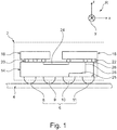
- the figure 1 represents a portion of a system 2 soldered to a printed circuit 4 or PCT (“Printed Circuit Board”) by means of an array 6 of solder balls (in English, “Solder bumps”). To simplify the illustration, only four balls 8 to 11 of the array 6 are shown.
- the system 2 is typically in the form of a parallelepiped housing inside which electronic and optical chips are housed. Only the solder balls of the system 2 protrude on a lower face of this housing. To simplify the illustration, this box has not been shown on the figure 1 .
- System 2 in its case is known by the English name of 'system in package'. More generically, the system 2 is also often referred to by the term “integrated circuit”.
- the horizontal is defined in the figures by X and Y directions of an orthogonal frame of reference R.
- the Z direction of the frame of reference R corresponds to the vertical direction.
- Terms such as “lower”, “upper”, “above”, “below”, “top” and “bottom” are defined with respect to this Z direction.
- system 2 comprises a support 14.
- the balls of the array 6 are placed directly on the underside of the support 14.
- the assembly of the support 14 and of the array 6 is known by the acronym BGA ("Ball Grid Array ”).
- BGA All Grid Array
- the upper face of the support 14 has pads on which chips electronics and / or photonics can be soldered.
- system 2 comprises an electronic chip 16 and a photonic chip 18. These two chips 16 and 18 are both directly welded to the upper face of the support 14.
- the electronic chip only comprises electronic components connected to each other to perform predetermined functions.
- the electronic chip 16 therefore has no optical component.
- the photonic chip 18 has no electronic component.
- the photonic chip 18 and the electronic chip 16 of the system 2 are electrically connected to pads on the upper face of the support 14.
- the chips 16 and 18 are also electrically connected to the printed circuit. 4.
- the chips 16 and 18 are welded to respective pads of the upper face of the support 14 by means of networks, respectively 20 and 22, of solder beads.
- the networks 20 and 22 are represented by some of these solder microspheres located under the chips 16 and 18.
- the solder microbeads are known by the English term of “C4 Bumps”.
- the support 14 comprises electrical connections which extend mainly horizontally, such as a connection 24.
- the connection 24 electrically connects certain pads of the upper face of the support 14 to each other in order to allow the exchange of electrical or power signals. electrical between the chips soldered on these pads.
- the support 14 is also crossed by vertical connections, such as connections 26 and 28.
- these vertical connections lead to a horizontal metal line of a redistribution layer better known by the acronym RDL (“Redistribution layer”). .
- RDL redistribution layer
- the horizontal lines of the redistribution layer electrically connect some of the vertical connections to corresponding solder balls of the network 6.
- the vertical connections make it possible in particular to supply the chips 16 and 18 with electricity and, also, to exchange electrical signals with d 'other chips soldered on the printed circuit 4.
- the support 14 is generally devoid of any other electrical or optical component.
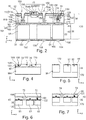
- the layers 36 and 38 are directly bonded to one another at the level of a bonding interface 40 which extends essentially in a horizontal plane.
- the upper face of the layer 38 corresponds to the upper face 32 and the lower face of the layer 36 corresponds to the lower face 34.
- Layer 36 is mainly made of a non-conductive material.
- non-conductive material denotes a material whose conductivity at 20 ° C. is less than 10 -1 or 10 -2 S / m.
- this non-conductive material can be a semiconductor material such as undoped silicon or an electrically insulating material such as glass.
- the non-conductive material is undoped crystalline silicon.
- conductive material or “electrically conductive material” denotes a material whose electrical conductivity at 20 ° C. is generally greater than 10 5 or 10 6 S / m.
- the layer 36 comprises a sublayer 42 of undoped crystalline silicon and a surface sublayer 44 produced directly on the sublayer 42.
- the sublayer 44 is made of silicon dioxide.
- the lower face of the sublayer 42 corresponds to the face 34.
- the thickness of the sublayer 42 is large enough to be rigid enough and not to have too great a deflection. In particular, the thickness of the sublayer 42 is sufficient to make it possible to handle the chip 18. For this purpose, the thickness of the sublayer 42 is greater than 50 ⁇ m or 80 ⁇ m or 100 ⁇ m.
- the sublayer 42 comprises via, called hereinafter “primary via” which make it possible to form electrical connections which vertically pass through the substrate 30.
- Each primary via extends from a lower end to an upper end. The lower end is flush with the lower face 34. The upper end is flush with the bonding interface 40. These primary via therefore pass through the entire thickness of the interconnection layer 36. On the other hand, the primary via do not cross and do not penetrate inside the optical layer 38.
- Layer 36 does not contain a layer of buried silicon oxide. Its minimum thickness giving rise to an acceptable deflection is therefore less than that of a layer which would contain such a layer of buried silicon oxide. Having a lesser thickness makes it possible in particular to reduce the parasitic capacitances of the primary via which is proportional to the height of the primary via. Thus, preferably, the thickness of the sub-layer 42 is also less than 150 ⁇ m or 100 ⁇ m.
- the figure 2 represents only three primary via 50-52. However, in general, layer 36 has a much larger number of primary via. By For example, all the primary via are identical so that subsequently only the primary via 50 is described in more detail.
- the primary via 50 is carried out in a conventional manner.
- the reader can consult the following article: Ken Miyairi et Al: “Full integration and electrical characterization of 3D Silicon Interposer demonstrator incorporating high density TSVs and interconnects”, 45th International Symposium on Microelectronics, 2012 .
- Ken Miyairi et Al “Full integration and electrical characterization of 3D Silicon Interposer demonstrator incorporating high density TSVs and interconnects”
- the lower part 54 extends vertically from the lower end of the via 50 to the upper part 56.
- the horizontal section of the lower part is substantially constant over its entire height. Its height and its diameter are subsequently denoted, respectively, H1 and D1.
- the lower portion 54 passes through at least 80% and preferably at least 90% or 95% of the thickness of the layer 36. Since the thickness of the layer 36 is large, the diameter D1 is also important for whether the aspect ratio H1 / D1 is less than 10/1 or 8/1. Indeed, it is difficult to manufacture via having an aspect ratio greater than 10/1.
- the height H1 is greater than 80% or 90% or 95% of the thickness of the underlayer 42. Under these conditions, the height H1 is between 80 ⁇ m and 142.5 ⁇ m and, generally, between 95 ⁇ m and 130 ⁇ m.
- the diameter D1 is then typically between 10 ⁇ m and 20 ⁇ m.
- metal via denotes a via made of metal and the diameter of which is small, that is to say the diameter of which is less than 3 ⁇ m and, generally, less than 1 ⁇ m.
- the height of a metal via is also small, that is to say less than 3 ⁇ m or 1 ⁇ m.
- the metal is copper.
- the structure of such an interconnection metal network is well known to those skilled in the art. This is the redistribution layer interconnect metal network or RDL.
- the thickness of the sublayer 44 is typically less than 10 ⁇ m or 3 ⁇ m.
- the diameter of the upper part 56 is equal to the largest diameter of a metal via which composes it.
- the diameter of the upper part 56 is therefore less than 10 ⁇ m and generally less than 3 ⁇ m or 1 ⁇ m.
- the optical layer 38 comprises at least one optical component buried inside this layer.
- the optical component is chosen from the group consisting of an optical modulator, a laser source, a waveguide, a photodetector, a demultiplexer and an optical multiplexer. Of the optical components in this group, all are active optical components except the waveguide.
- Component 70 is a laser source and component 72 is an optical modulator.
- the component 72 is capable of modifying, as a function of an electrical control signal, the phase, the amplitude or the intensity of an optical signal which passes through it.
- Such optical modulators are well known so that component 72 is not described here in detail.
- Component 72 comprises an electrical contact 74 intended to receive the electrical control signal.
- this electrical contact 74 is buried inside the optical layer 38.
- the electrical contact 74 is located on a lower face of the component 72. The electrical contact 74 is therefore turned towards the interface 40. lift-off. In this configuration, the electrical contact 74 is only accessible from below the optical component 72.
- Component 70 also includes an upper socket 84 and a lower socket 86 directly in contact, respectively, with the upper 82 and lower 78 layers.
- the active layer 80 generates the optical signal emitted by the component 70 when an appropriate potential difference is applied between the taps 84 and 86.
- the lower layer 78 is optically coupled to the waveguide 76.
- the layer 78 is disposed above the waveguide 76 and separated from this waveguide 76 by a thin sublayer 90 d. buried oxide.
- the thickness of the oxide sublayer 90 is less than 100 nm and, preferably, less than 50 nm or 20 nm.
- the waveguide 76 and the optical component 72 are buried within an encapsulation sublayer 122 located directly below the oxide sublayer 90. More specifically, the sublayer 122 extends from a sublayer 120 up to the sublayer 90. The sublayer 122 is broken down here into an upper level 92 of optical guidance and into a lower level 94 of electrical interconnection. Level 92 includes all the optical components and parts of optical components made under the sublayer 90. Level 92 therefore here includes the waveguide 76, the optical component 72 and a dielectric material in which the optical components and parts of optical components are encapsulated. For example, this level 92 is fabricated from a crystalline silicon sublayer in which the waveguide 76 and component 72 have been fabricated before being encapsulated in the dielectric material.
- Level 94 is devoid of optical component and optical component part.
- level 94 has metal interconnect arrays encapsulated in a dielectric material as will be described later.
- the dielectric material of the sublayer 122 has a refractive index lower than the refractive index of the material used to make the waveguide 76 and the component 72.
- the dielectric material is silicon dioxide.
- the layers 78, 80 and 82 are for their part made in a sublayer 128 located directly on the sublayer 90.
- the sublayer 128 here comprises a III-V material in which the layers 78, 80 and 82 are made. and a dielectric material which encapsulates layers 78, 80 and 82.
- Sublayer 128 extends horizontally directly above sublayer 90 and its upper face corresponds to face 32.
- this layer 38 includes via, called “secondary via”.
- Each secondary via extends a primary via inside the optical layer 38.
- each secondary via extends from the bonding interface 40 towards the inside of the layer 38.
- the diameter of the secondary via is much smaller than the diameter of the primary via.
- the diameter of the secondary via is less than 3 ⁇ m and, preferably, less than 1 ⁇ m.
- the thickness of the layer 38 is less than 15 ⁇ m or or 8 ⁇ m or 5 ⁇ m.
- the secondary via are classified into two categories.
- a first category called “secondary crossing via” and a second category called “secondary non-crossing via”.
- the secondary via through the thickness of the layer 38 and therefore, in particular, the level 92 of optical guidance. They therefore extend vertically from the bonding interface 40 to the upper face 32. They are typically used to electrically connect the electrical tracks formed on the upper face 32 to one of the primary via. Conversely, the non-traversing secondary via do not completely pass through the thickness of the layer 38 and, in particular, do not pass through the level 92 of optical guidance. They therefore extend from the bonding interface 40 to an electrical contact, such as contact 74, buried inside. of layer 38.
- the figure 2 represents two through secondary via 100 and 102.
- the via 100 electrically connects the primary via 50 to an electrical track 106 made on the face 32.
- the track 106 electrically connects the upper end of the via 100 to the socket 84.
- the lower end of via 100 is in direct mechanical and electrical contact with metal line 58.
- the through secondary via 102 electrically connects the primary via 51 to an electrical track 108 made on the face 32.
- the track 108 electrically connects the end of the via 102 to the socket 86.
- the lower end of the via 102 is directly in mechanical contact. and electrical with the metal line from via 51.
- via 100 and 102 are used to power component 70.
- via 102 The structure of via 102 is identical to that of via 100. Thus, only the structure of via 100 is described below in more detail.
- the via 100 has a lower part 110 and an upper part 112 arranged immediately one above the other. Parts 110 and 112 are made, during manufacture, from opposite sides of the optical layer.
- the diameter of the lower part 110 is defined in the same way as for the upper part 58 of the primary via 50.
- the diameter of the part 110 is less than 3 ⁇ m or 1 ⁇ m.
- the interconnecting metal network that forms part 110 has only two levels of metal lines. For example, these are the levels often designated by the references M4 and M5.
- this part 110 is low, that is to say less than 6 ⁇ m or 3 ⁇ m or 1 ⁇ m.
- the metal line 116 is produced in a silicon oxide sublayer 120, the lower face of which coincides with the bonding interface 40.
- the sublayer 120 is produced directly under the sublayer 122.
- the sublayer 120 is made of silicon dioxide.
- Metal via 118 are located inside level 94 of sublayer 122.
- the upper part 112 of the secondary via 100 is formed by a coating 124 of conductive material.
- the coating 124 is made of copper or aluminum.
- This coating 124 continuously covers the vertical walls and the bottom of a hole 126 dug in the layer 38. More precisely, the hole 126 extends from the upper face 32 to the metal line 114. For this, the hole 126 successively passes from the top to the bottom, the encapsulation layer 128, the sublayer 90, the level 92 of optical guidance and a part of the level 94 of the sublayer 122.
- the maximum diameter of hole 126 is less than 3 ⁇ m and, preferably, less than 1 ⁇ m.
- the maximum diameter of the upper part 112 of the secondary via 100 is also less than 3 ⁇ m or 1 ⁇ m.
- the coating 124 is in direct mechanical and electrical contact with the track 106 and, in its lower part, in direct mechanical and electrical contact with the metal line 114.
- the coating 124 does not fill the entire hole 126.
- the center of the hole 126 is therefore hollowed out.
- the thickness of the coating 124 is less than 500 nm or 300 nm.
- the center of hole 126 is filled with an electrically non-conductive and passivating material.
- the coefficient of expansion of this electrically non-conductive material is less than 0.8C 124 , and preferably less than 0.5C 124 or 0.3C 124 , where C 124 is the coefficient of thermal expansion of the coating 124.
- the center of the hole 126 is filled with the same dielectric material as that of the sub-layer 122, that is to say silicon dioxide.
- Layer 38 also includes a non-traversing secondary via 130.
- Via 130 electrically connects electrical contact 74 to the upper end of primary via 52 to receive the electrical control signal from optical component 72.
- via 130 extends vertically from the bonding interface 40 to the electrical contact 74. It therefore completely passes through the sublayer 120 and the level 94 of the sublayer 122. On the other hand, it does not cross the guide level 92 optics or the sublayer 90.
- the via 130 does not open into the upper face 32 unlike a secondary through via.
- the metal line 138 is in direct mechanical and electrical contact on the upper end of the primary via 52.
- the interconnecting metal network has five different levels of metal lines. For example, these five levels of metal lines are often designated by the references, respectively, M1 to M5.
- the diameter of via 130 is also less than 3 ⁇ m or 1 ⁇ m.
- Redistribution lines 150 are made on the underside 34 to connect electrically the lower ends of the primary via to corresponding solder beads. To this end, the redistribution lines include connection pads to which the solder microspheres are directly fixed. On the figure 1 , only three solder beads 152 to 154 are shown. These microbeads 152 to 154 are intended to be welded to corresponding pads on the upper face of the support 14 and therefore form part of the network 22 of welding microbeads.
- the lines 150 are buried inside an encapsulation layer 156 made of an electrically non-conductive material such as a polymer.
- the stack of sublayers 90, 122 and 120 is manufactured on a handle 164 ( figure 4 ) then provided.
- this stack constitutes only a part of the optical layer because it lacks, at this stage, in particular, the layer 128.
- the sublayer 120 is located on the side opposite the handle 164 and has a face 166 of collage. This face 166 is suitable for being bonded to another substrate by direct bonding, that is to say by bonding which does not require the addition of material.
- the underlayer 90 is directly attached to the handle 164.
- the handle 164 is a support which allows easy handling of the stack of the underlayer 120, 122 and 90.
- the thickness of the handle 164 is typically greater than 250 ⁇ m or 500 ⁇ m.
- the handle 164 is a silicon substrate with a thickness of 750 ⁇ m or 775 ⁇ m.
- the sublayer 90 is the buried oxide layer of a substrate known by the acronym SOI (“Silicon On Insulator”).
- SOI Silicon On Insulator
- the waveguide 76 and the component 72 are produced, typically by etching, in the monocrystalline silicon layer of this SOI substrate.
- the waveguide 76 and the optical component 72 are buried in the dielectric material of the sublayer 122 by successively depositing several layers of oxide one after the other. others.
- the interconnecting metal networks forming the secondary via 130 and the lower parts 110 of the secondary via 100 and 102 are produced.
- these interconnecting metal networks are made from the side opposite to the handle 164.
- the methods of making the optical components on the sublayer 90, the methods of burying components inside the sublayer. layer 122 and the methods of making interconnecting metal networks are well known and are therefore not described in more detail here. Note that at this stage of the manufacturing process, the production of the upper parts 112 of the secondary via 100 and 102 is impossible. The sublayer 122 therefore does not include, at this stage, the upper parts 112 of the via 100 and 102.
- the interconnection layer 36 is fabricated on a handle 170 ( figure 5 ) then provided.
- the layer 36 has an outer face 172 located on the side opposite to the handle 170.
- This face 172 is a bonding face, that is to say capable of being bonded, by direct bonding, to the face 166.
- the thickness of the handle 170 is greater than 250 ⁇ m or 500 ⁇ m to allow easy handling of the layer 36.
- the handle 170 is for example a silicon substrate.
- Step 162 also comprises the production of primary via 50 to 52 in the layer 36.
- the layer 36 comprises these primary via 50 to 52.
- the production of such a layer 36 on the handle 170 and the realization of the via 50 to 52 in this layer 36 are conventional.
- parts 54 of vias 50 to 52 consist of a coating of dielectric material, covered with a barrier layer of titanium or tantalum, and filled with copper. A method of manufacturing these parts 54 is for example described in the article by Ken Miyairi cited above.
- the metal via 60 are made, in electrical contact with the parts 54 of the primary via.
- the metal lines, such as the metal line 58 are produced and then encapsulated in the sublayer 44 of oxide. The outer face of the sublayer 44 is then prepared for its direct bonding to the face 166.
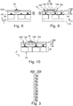
- the faces 166 and 172 are glued, by direct gluing, one on the other. This is shown on the figure 6 .
- the bonding interface 40 is then obtained.
- it is a direct hybrid copper-oxide bond as described in the following article: Yan Beillard et Al: “Chip to wafer copper direct bonding electrical characterization and thermal cycling”, 3D Systems Integration Conference (3DIC), 2013 IEEE International .
- handle 164 is removed to expose the underlayer 90 ( figure 7 ).
- handle 164 is removed by mechanical and chemical polishing known by the acronym CMP ("Chemical Mechanical Polishing"), followed by selective chemical etching.
- CMP Chemical Mechanical Polishing
- the light amplifying part of the component 70 is produced on the sub-layer 90, on the side opposite to the optical guidance level 92 ( figure 8 ) and encapsulated in the dielectric material of the encapsulation layer 128.
- the sockets 84, 86, the electrical tracks 106 and 108 and the upper parts 112 of the secondary via 100 and 102 are produced ( figure 9 ).
- holes such as hole 126 are first dug through sublayers 128, 90 and level 92 of sublayer 122.
- a coating of conductive material is deposited over the entire exterior face.
- this conductive coating is etched so that the conductive coating only remains locations of the taps 84, 86, of the tracks 106 and 108 and of the upper parts 112 of the secondary via 100 and 102.
- the production of the layer 38 is then finished.
- the handle 170 is then withdrawn in turn to expose the lower face 34 ( figure 10 ).
- the redistribution lines 150, the solder microbeads 152 to 154 and the encapsulation layer 156 are produced on the lower face 34 exposed. The manufacture of the photonic chip 18 is then completed.
- the electronic chip 16 and the photonic chip 18 are welded to pads on the upper face of the support 14.
- the chips 16 and 18 are then electrically connected to each other via the horizontal connections of the support 14.
- the support 14 and the chips 16 and 18 are encapsulated in an electrically non-conductive material and a good thermal conductor, such as an epoxy resin.
- a cover on which is disposed a heat sink, such as a heat sink is fixed to the upper faces of the chips 16 and 18.
- This cover is for example glued, using a thermally glue.
- conductive directly on the upper face 32 of the photonic chip 18 and the upper face of the chip 16.
- these upper faces can be directly in contact with the thermal adhesive which is in contact with the cover. This is made possible by the fact that all electrical signals and power supplies are brought through the undersides of chips 16 and 18.
- the system 2 is for example soldered to the printed circuit 4.
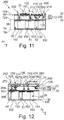
- the optical layer 202 is identical to the optical layer 38 except that it additionally comprises an active electronic component 210 buried inside the level 92 of the sublayer 122.
- This electronic component 210 is qualified as active because, for to function, it needs to be supplied with electricity, and it emits and / or receives an electric signal.
- the component 210 comprises an electrical contact 212 on its lower face. This electrical contact 212 is therefore buried inside the sublayer 122 and turned towards the bonding interface 40.
- the secondary via 204 electrically connects the electrical contact 212 of the electronic component 210 to the primary via 52 by crossing only the lower level 94 of the sublayer 122 and the sublayer 120.
- the electronic component 210 is, for example, intended for in supplying, from an electrical signal which it receives via the primary via 52, an electrical control signal to the optical component 72.
- the component 210 comprises on its lower face another electrical contact connected to the contact 74 of the component 72.
- the interconnection metal network located inside the level 94 of the sublayer 122 is modified to create a path which electrically connects together this other electrical contact and the contact 74. To simplify the figure 11 , this modification of the metal interconnection network has not been shown on the figure 11 .
- the structure and manufacture of via 204 can be deduced from the explanations given for via 130.
- Via 206 is a via which electrically connects a metal line 135, buried within level 94 of sublayer 122, to an electrical track 216 made on the upper face 32. Via 206 extends vertically from the face 32 up to the line 135 of buried metal, crossing in particular the sublayer 90 and the level 92 of optical guidance.
- the electrical track 216 comprises a test pad which makes it possible to test the correct operation of the components 210 and / or 72 during the manufacturing process of the photonic chip 200 and, in particular, before the removal of the handle 170.
- the interconnecting metal network located inside level 94 of sublayer 122, is also modified to create, using metal lines and metal via, an electrical path that electrically connects the electrical contacts 212 and / or 74 to the metal line 135.
- via 206 is here identical to that of via 100 except that it does not have a lower part 110.
- via 206 is manufactured in the same way as the upper part 112 of via 100 and generally at the same time as this. upper part 112.
- the through secondary via 252 and 254 are identical, respectively, to via 100 and 102 except that their upper part 270 is made differently. More precisely, the upper part 270 is here a solid via. In other words, the upper part 270 is identical to the upper part 112, except that the central recess of the hole 126 is filled with a conductive material. Generally, in this case, the maximum diameter of the upper part 270 of the via 252 and 254 is less than 1 ⁇ m.
- the laser source 256 is identical to the component 70, except that the socket 86 is replaced by a socket 274.
- the socket 274 is a metallic via which electrically connects the layer 78 to the electrical track 108.
- the underside of the waveguide 76 of the laser source 256 also has an electrical contact 264.
- This electrical contact 264 is connected thermally to the interconnect layer 36 through a non-traversing via 266.
- Via 266 is structurally identical, for example, to via 130. However, unlike via 130, via 266 does not necessarily have to be function of electrically connecting the contact 264 to a primary via of the layer 36.
- the lower end of the via 264 is directly in mechanical and electrical contact with a metal line, located inside the sublayer 44, which is flush with interface 40. This metal line is here electrically isolated from all the primary via.
- Via 266 is here made of a material which is a good thermal conductor.
- a “good thermal conductor” material is typically a material whose thermal conductivity is greater than 1.2C 122 , and preferably greater than 2C 122 or 3C 122 , where C 122 is the thermal conductivity of the dielectric material of the sublayer 122.
- the material used to make via 266 is the same as that used to make via 130.
- the presence of via 266 improves the thermal dissipation of the heat produced by laser source 256. Indeed, it is known to the industry. those skilled in the art that the waveguide 76 sees its temperature increase during the operation of the laser source 256. In the absence of the via 266, the presence of the dielectric material of the sublayer 122 under the waveguide 76 does not does not effectively evacuate the heat produced.
- the via 266 produces a thermal bridge, here made of metal, through the sub-layer 122 which thermally connects the waveguide 76 to the layer 36. This makes it possible to more efficiently remove the heat produced by the laser source 256.
- the through secondary via 258 electrically and directly connects the primary via 52 to an electrical track 276 produced on the upper face 32.
- the track 276 comprises a pad on which is welded a first electrical contact of the electronic chip 260.
- the structure of the via 258 is here identical to that of via 252.
- the via 262 electrically connects directly an electrical track 280 made on the upper face 32 to the metal line 135 buried inside the level 94 of the sublayer 122.
- the structure of via 262 is identical to the structure of via 252 except that the lower part 110 is omitted.
- the electrical track 280 comprises a pad on which is welded a second electrical contact of the electronic chip 260.
- metal line 135 is electrically connected to the electrical contact 74 of the optical component 72 via an interconnecting metal network similar to that described with reference to figure 11 .
- electronic chip 260 is a transducer, electrically powered by primary via, which controls optical component 72 based on electrical signals received via primary via, e.g., 52.
- the horizontal cross section of a via is not necessarily circular.
- the cross section of a via can be square or rectangular.
- the term “diameter” denotes the hydraulic diameter of this horizontal cross section.
- the diameter of the via is not necessarily constant over its entire height.
- the term “diameter” of the via denotes the largest diameter of this via along its height.
- the upper portion 56 of the primary via is omitted.
- the upper end of part 54 of the primary via is directly flush with the bonding interface 40.
- the metal via 60 are omitted.
- the upper end of the part 54 is in direct mechanical and electrical contact with the metal line 58.
- the upper part 56 of a primary via may include several additional lines of metal made at different depths inside the sublayer 44.
- the different levels of metal lines of the part 56 are then electrically connected to each other by metal via.
- These additional metal lines then form a redistribution layer or RDL which makes it possible, for example, to electrically connect together several metal lines which are flush with the interface 40.
- the interconnecting metal network used to form the lower portion of a secondary through via may also, alternatively, have more than three levels of metal lines.
- a secondary through via is omitted.
- the bottom of the hole 126 then opens directly onto the metal line 58 of the primary via.
- Such a secondary crossing via then has only one part, namely part 112.
- the center of the hole 126 can also be filled with a dielectric material different from the dielectric material of the sublayer 122.
- a dielectric material different from the dielectric material of the sublayer 122.
- it is filled with an organic material.
- the interconnection layer 36 can be made from materials other than silicon.
- it is made of glass.
- layer 36 comprises one or more electronic components.
- the sublayers of optical layer 38 can also be made from other materials.
- the sublayer 122 can be produced using another dielectric material such as, for example, amorphous silicon, silicon nitride SiN or silicon nitride oxide SiON.
- the different oxide sublayers of layer 38 are not necessarily all made from the same oxide.
- the sublayer 120 is produced in an oxide different from that used to produce the sublayer 90. It is also possible to use an oxide to produce the sublayer 122 which is different from that of the sublayer. layer 90.
- the optical layer can also be crossed by additional via whose diameter is greater than 3 ⁇ m and, for example, greater than 10 ⁇ m or 20 ⁇ m.
- additional via whose diameter is greater than 3 ⁇ m and, for example, greater than 10 ⁇ m or 20 ⁇ m.
- a large surface exclusion zone is provided around each of these additional via and no optical component is made inside this exclusion zone.
- This exclusion zone is sized in accordance with the teaching given in the previously cited Yang2013 article.
- the photonic chip includes some of these additional via, the implantation of the optical components in the optical layer is still simplified because of the presence of secondary via which nevertheless limits the constraints on the placement of the optical components. .
- the number of optical components buried within level 92 of sublayer 122 can be any.
- the various optical components are not necessarily buried inside level 92 at the same depth. This is especially the case if the optical components or parts of optical components are made from different sub-layers of material stacked on top of each other. These material sub-layers can then be chosen from the group consisting of a crystalline silicon sub-layer, an amorphous silicon sub-layer, a silicon nitride sub-layer SiN and a sub-layer. -silicon nitride oxide layer SiON.
- component 70 or laser source 256 is omitted.
- the encapsulation layer 128 can also be omitted so that the upper face 32 then corresponds to the upper face of the sublayer 90.
- the lower end of secondary via 266 is electrically and mechanically connected to at least one primary via.
- This primary via is then not necessarily used to establish an electrical connection but above all to improve the thermal dissipation of the heat produced by the laser source.
- the diameter of via 266 is not necessarily less than 3 ⁇ m or 1 ⁇ m. Its diameter can also be greater than these values.
- via 266 to improve the dissipation of the heat produced by a laser source is similarly applicable to the improvement of the heat produced by any type of optical or electronic component of which at least a part is buried in the interior of sublayer 122.
- a via similar to via 266 can also be used to dissipate the heat produced by optical component 72 or electronic component 210.
- the photonic chip may include an electrical track produced on the upper face 32 which is not necessarily used to electrically connect an optical component to one of the primary via.
- an electrical track 276 can only be used to electrically connect an electronic chip soldered on the upper face 32 of the photonic chip to one of the primary via.
- the photonic chip only comprises non-traversing secondary via.
- all of the non-through secondary via are made from the side opposite to the handle 164.
- the handle removal order can then be reversed.
- the handle 170 can be removed before the handle 164.
- the non-crossing secondary via is entirely manufactured before the bonding of the layer 38 on the layer 36.
- the photonic chip has only secondary through vias.
- chip 260 can correspond to chip 16 of the figure 1 .
- the electronic chip 260 is an ASIC supplied electrically by means of the primary via, and which controls the optical component 72 with the electric signals which it generates.
- thermally connecting a part of the component 70 or of the laser source 256 to the interconnection layer via secondary, typically non-traversing via, such as via 266, can be implemented independently of the other characteristics described. here of the photonic chip. In particular, this can be implemented in a context where the primary via passes through the optical layer as described in the article Yang2013 or in a context where all the primary via are omitted.
- the primary via do not generate substantial mechanical stress on the optical components.
- the interconnection layer 36 is totally devoid of optical component. These are only located inside the diaper. Therefore, the optical components can be implanted with respect to each other without worrying about the arrangement of the primary via. In particular, it is not necessary to respect any exclusion zone around each primary via.
- the secondary via passing through the optical guidance level 92 have a diameter preferably less than or equal to 3 ⁇ m, or even 1 ⁇ m. Such secondary through vias can thus be placed 4 ⁇ m or even 2 ⁇ m away from the optical components without generating mechanical stresses on the latter.
- the through vias described in Yang2013 must be placed 40 ⁇ m from the optical components so as not to constrain them mechanically. It is therefore possible to place the optical components much closer to the secondary via than what would have been possible if their diameter had been equal to the diameter of the primary via.
- the combination in the same photonic chip of primary via and secondary via therefore makes it possible to obtain a sufficiently thick photonic chip to have an acceptable deflection while limiting the constraints to be observed in order to place the optical components with respect to the via.
- the interconnection layer does not necessarily contain a layer of buried silicon oxide. Its minimum thickness giving rise to an acceptable deflection is therefore less than that of a layer which would contain a buried silicon oxide. Having a lesser thickness of the interconnection layer makes it possible in particular to reduce the parasitic capacitances of the primary via. Indeed, this parasitic capacity is proportional to the height of the primary via.
- the fact of placing the laser source on the upper face of the oxide layer 90 facilitates its cooling from the outside, in particular thanks to the casing of the system.
- the center of the hole 126 is filled with an electrically non-conductive material whose coefficient of thermal expansion is smaller than that of the coating 124 makes it possible to further limit the mechanical stresses exerted by the secondary via on the optical components located near.
Landscapes
- Physics & Mathematics (AREA)
- Condensed Matter Physics & Semiconductors (AREA)
- General Physics & Mathematics (AREA)
- Electromagnetism (AREA)
- Optics & Photonics (AREA)
- Optical Integrated Circuits (AREA)
- Optical Couplings Of Light Guides (AREA)
- Semiconductor Lasers (AREA)
- Optical Modulation, Optical Deflection, Nonlinear Optics, Optical Demodulation, Optical Logic Elements (AREA)
- Production Of Multi-Layered Print Wiring Board (AREA)
- Internal Circuitry In Semiconductor Integrated Circuit Devices (AREA)
- Light Receiving Elements (AREA)
Claims (13)
- Photonischer Chip, der sich im Wesentlichen in einer "Ebene des Chips" genannten Ebene erstreckt, wobei dieser photonische Chip aufweist:- ein Substrat (30), das eine Oberseite (32) und eine Unterseite (34) parallel zur Ebene des Chips aufweist, wobei dieses Substrat zwischen der Ober- und Unterseite aufweist:• eine Verbindungsschicht (36) einer Dicke von mehr als 50 µm, wobei diese Verbindungsschicht kein optisches Bauteil aufweist,• eine optische Schicht (38; 202), die im Bereich einer Klebeverbindungsfläche (40) auf die Verbindungsschicht geklebt ist,• mindestens ein optisches Bauteil (70, 72; 256), das innerhalb der optischen Schicht (38; 202) eingegraben ist,• einen elektrischen Anschluss ausgewählt aus der Gruppe, die aus einem im Inneren der optischen Schicht (38; 202) vergrabenen elektrischen Kontakt (74; 212; 264), wobei dieser vergrabene elektrische Kontakt derjenige des optischen Bauteils (72) oder eines elektronischen Bauteils (210) ist, und aus einem Strompfad (106, 108; 276, 280) besteht, der an der Oberseite des Substrats hergestellt ist,- elektrische Anschlusskontaktstellen, die an der Unterseite des Substrats hergestellt sind, wobei jede dieser Kontaktstellen mittels einer Lötperle (152-154) elektrisch mit einem anderen Träger (14) verbunden werden kann,- eine Primärdurchkontaktierung (50-52), die sich von der Unterseite (34) durch die Verbindungsschicht hindurch erstreckt, um eine der Anschlusskontaktstellen elektrisch an den elektrischen Anschluss anzuschließen, wobei diese Primärdurchkontaktierung einen Durchmesser größer als oder gleich 10 µm hat,dadurch gekennzeichnet, dass:- die Dicke der optischen Schicht (38; 202) geringer als 15 µm ist,- die Primärdurchkontaktierung (50-52) sich durch die Verbindungsschicht hindurch nur zwischen der Unterseite (34) und der Klebeverbindungsfläche (40) erstreckt, so dass die Primärdurchkontaktierung sich nicht ins Innere der optischen Schicht (38; 202) verlängert, und- der photonische Chip eine Sekundärdurchkontaktierung (100, 102, 130; 204; 252, 254, 258) aufweist, die die Primärdurchkontaktierung im Inneren der optischen Schicht verlängert, um die Primärdurchkontaktierung elektrisch an den elektrischen Anschluss anzuschließen, wobei diese Sekundärdurchkontaktierung sich im Inneren der optischen Schicht (38; 202) von der Klebeverbindungsfläche (40) bis zum elektrischen Anschluss erstreckt, wobei der maximale Durchmesser dieser Sekundärdurchkontaktierung geringer als 3 µm ist.
- Photonischer Chip nach Anspruch 1, wobei- der elektrischer Anschluss der an der Oberseite des Substrats hergestellte Strompfad (106, 108; 276, 280) ist,- der photonische Chip eine im Inneren der optischen Schicht (38; 202) vergrabene Metallleitung (114) aufweist, wobei diese vergrabene Metallleitung sich hauptsächlich in einer Ebene parallel zur Ebene des Chips erstreckt,- die Sekundärdurchkontaktierung aufweist:• einen ersten Teil (110) der Sekundärdurchkontaktierung, der sich durch die optische Schicht hindurch von der Klebeverbindungsfläche bis zur vergrabenen Metallleitung erstreckt, und• einen zweiten Teil (112) der Sekundärdurchkontaktierung, der sich durch die optische Schicht hindurch von der vergrabenen Metallleitung bis zum elektrischen Anschluss erstreckt, wobei dieser zweite Teil der Sekundärdurchkontaktierung die vergrabene Metallleitung (114) elektrisch an den elektrischen Anschluss anschließt.
- Photonischer Chip nach Anspruch 2, wobei- der erste Teil (110) der Sekundärdurchkontaktierung metallische Durchkontaktierungen (118) aufweist, die Metallleitungen (114, 116) elektrisch aneinander anschließen, die sich hauptsächlich parallel zur Ebene des Chips erstrecken, wobei diese Metallleitungen im Inneren der optischen Schicht (38; 202) übereinander angeordnet sind, wobei der größte Durchmesser dieser metallischen Durchkontaktierungen kleiner als 3 µm ist, und- der zweite Teil (112) der Sekundärdurchkontaktierung eine Beschichtung (124) aus leitendem Material aufweist, die auf eine Wand eines Lochs (126) aufgebracht ist, wobei dieses Loch ausgehend von der Oberseite bis zur Metallleitung (114) ausgehöhlt ist und in seiner Mitte mit einem elektrisch nicht leitenden Material gefüllt ist, wobei der Wärmedehnungskoeffizient dieses elektrisch nicht leitenden Materials niedriger als 0,8C124 ist, wobei C124 der Wärmedehnungskoeffizient der Beschichtung ist.
- Photonischer Chip nach Anspruch 1, wobei der elektrische Anschluss der vergrabene elektrische Kontakt (74; 212) des optischen (72) oder elektronischen (210) Bauteils ist.
- Photonischer Chip nach Anspruch 4, wobei die Sekundärdurchkontaktierung (130) sich durch die optische Schicht hindurch von der Klebeverbindungsfläche direkt bis zum elektrischen Anschluss (74; 212) erstreckt, um diesen elektrischen Anschluss elektrisch an die Primärdurchkontaktierung anzuschließen.
- Photonischer Chip nach Anspruch 1, wobei:- der elektrische Anschluss der vergrabene elektrische Kontakt (74; 212) des optischen (72) oder elektronischen (210) Bauteils ist,- der photonische Chip aufweist:• einen an der Oberseite des Substrats hergestellten Strompfad (216),• eine im Inneren der optischen Schicht vergrabene Metallleitung (135), wobei diese Metallleitung elektrisch an den elektrischen Anschluss angeschlossen ist und sich hauptsächlich parallel zur Ebene des Chips erstreckt,• eine Tertiärdurchkontaktierung (206), die sich von der vergrabenen Metallleitung bis zu dem an der Oberseite des Substrats hergestellten Strompfad erstreckt, wobei der Durchmesser dieser Tertiärdurchkontaktierung kleiner als 3 µm ist.
- Photonischer Chip nach einem der vorhergehenden Ansprüche, wobei:- die optische Schicht von der Oberseite zur Klebeverbindungsfläche (40) nacheinander aufweist:• eine Oxid-Teilschicht (90), wobei mindestens ein Teil (76) des optischen (70, 72; 256) oder elektronischen (210) Bauteils auf der Seite dieser Oxid-Teilschicht (90) hergestellt ist, die zur Klebeverbindungsfläche (40) weist, und• eine Verkapselungs-Teilschicht (122), in der der mindestens eine Teil (76) des optischen oder elektronischen Bauteils in einem dielektrischen Material verkapselt ist,- der mindestens eine Teil (76) des optischen (70, 72; 256) oder elektronischen (210) Bauteils einen elektrischen Kontakt (264) aufweist, der innerhalb der Verkapselungs-Teilschicht (122) vergraben ist,- der optische Chip eine zusätzliche Durchkontaktierung (266) aufweist, die sich im Inneren der optischen Schicht von der Klebeverbindungsfläche (40) bis zum vergrabenen elektrischen Kontakt (264) des mindestens einen Teils (76) des optischen (256) oder elektronischen Bauteils erstreckt, wobei diese zusätzliche Durchkontaktierung aus einem Material hergestellt ist, dessen Wärmeleitfähigkeit höher als 1,2C122 ist, wobei C122 die Wärmeleitfähigkeit des dielektrischen Materials der Verkapselungs-Teilschicht (122) ist.
- Photonischer Chip nach Anspruch 7, wobei die zusätzliche Durchkontaktierung (266) von jeder Primärdurchkontaktierung elektrisch isoliert ist.
- Photonischer Chip nach Anspruch 7 oder 8, wobei das optische Bauteil, von dem mindestens ein Teil in der Verkapselungs-Teilschicht (122) verkapselt ist, eine Laserquelle (256) ist.
- Photonischer Chip nach einem der vorhergehenden Ansprüche, wobei der maximale Durchmesser der Sekundärdurchkontaktierung kleiner als 1 µm ist.
- Verfahren zur Herstellung eines photonischen Chips nach einem der vorhergehenden Ansprüche, dadurch gekennzeichnet, dass das Verfahren die folgenden Schritte aufweist:- die Bereitstellung (160) mindestens eines Teils der optischen Schicht (38; 202) befestigt an einem ersten Griff (164) einer Dicke von mehr als 250 µm, wobei der mindestens eine Teil der optischen Schicht (38; 202) mindestens ein optisches Bauteil (70, 72; 256) aufweist, das innerhalb dieses Teils der optischen Schicht (38; 202) eingegraben ist,- die Bereitstellung (162) der Verbindungsschicht einer Dicke von mehr als 50 µm befestigt an einem zweiten Griff (170) einer Dicke von mehr als 250 µm, wobei die Verbindungsschicht aufweist:• die Primärdurchkontaktierung (50-52), die die Verbindungsschicht durchquert, wobei diese Primärdurchkontaktierung dazu bestimmt ist, eine Anschlusskontaktstelle elektrisch an einen elektrischen Anschluss anzuschließen, der aus der Gruppe bestehend aus einem innerhalb der optischen Schicht (38; 202) vergrabenen elektrischen Kontakt (74; 212; 264), wobei dieser vergrabene elektrische Kontakt derjenige des optischen Bauteils (72) oder eines elektronischen Bauteils (210) ist, und einem an der Oberseite des Substrats hergestellten Strompfad (106, 108; 276, 280) ausgewählt wird, wobei diese Primärdurchkontaktierung einen Durchmesser von mehr als oder gleich 10 µm hat,• eine zweite Klebeseite (172) auf der dem zweiten Griff entgegengesetzten Seite, und• die kein optisches Bauteil aufweisende Verbindungsschicht, dann- das Kleben (174) der ersten Klebeseite auf die zweite Klebeseite, um die Klebeverbindungsfläche (40) zu erhalten, dann- das Entfernen (176) des ersten Griffs, um eine Oxid-Teilschicht (90) des mindestens einen Teils der optischen Schicht zu entblößen,- das Entfernen (182) des zweiten Griffs, um die Unterseite (34) des Substrats des photonischen Chips zu entblößen, dann die Herstellung der elektrischen Anschlusskontaktstellen auf dieser Unterseite, wobei jede dieser Kontaktstellen mittels einer Lötperle mit einem anderen Träger (14) verbunden werden kann,- vor oder nach dem Kleben die Herstellung (160, 180) einer Sekundärdurchkontaktierung, die die Primärdurchkontaktierung im Inneren der optischen Schicht verlängern kann, um die Primärdurchkontaktierung elektrisch an den elektrischen Anschluss anzuschließen, wobei diese Sekundärdurchkontaktierung sich im Inneren der optischen Schicht von der Klebeverbindungsfläche bis zum elektrischen Anschluss erstreckt, wobei der maximale Durchmesser dieser Sekundärdurchkontaktierung kleiner als 3 µm ist.
- Verfahren nach Anspruch 11, wobei die Herstellung der Sekundärdurchkontaktierung aufweist:- vor dem Kleben und vor dem Entfernen des ersten Griffs die Herstellung (160) eines ersten Teils der Sekundärdurchkontaktierung, wobei diese Herstellung eines ersten Teils der Sekundärdurchkontaktierung die Herstellung aufweist:• mindestens einer innerhalb des mindestens einen Teils der optischen Schicht vergrabenen Metallleitung (114) und einer Metallleitung (116), die die erste Klebefläche berührt, wobei jede dieser Metallleitungen sich hauptsächlich in einer Ebene parallel zur Ebene des Chips erstreckt, und• metallische Durchkontaktierungen (118), die die Metallleitungen elektrisch aneinander anschließen, und- nach dem Kleben und nach dem Entfernen des ersten Griffs, die Herstellung (180) ausgehend von der Oberseite des Substrats:• eines Strompfads auf dieser Oberseite, wobei dieser Strompfad den elektrischen Anschluss bildet, und• eines zweiten Teils der Sekundärdurchkontaktierung, der sich durch die optische Schicht hindurch von der vergrabenen Metallleitung bis zur Oberseite erstreckt, wobei dieser zweite Teil der Sekundärdurchkontaktierung die Metallleitung elektrisch an den elektrischen Anschluss anschließt.
- Verfahren nach Anspruch 12, wobei die Herstellung (180) des zweiten Teils der Sekundärdurchkontaktierung aufweist:- die Herstellung eines auf die vergrabene Metallleitung mündenden Lochs (126) ausgehend von der Oberseite, dann- das Abscheiden einer Beschichtung (124) aus elektrisch leitendem Material auf die Wände dieses Lochs, um die Metallleitung elektrisch an den elektrischen Anschluss anzuschließen, dann- das Abscheiden eines elektrisch nicht leitenden Materials in der Mitte dieses Lochs, um es wieder zu verschließen, wobei der Wärmedehnungskoeffizient dieses elektrisch nicht leitenden Materials niedriger als 0,8C124 ist, wobei C124 der Wärmedehnungskoeffizient der Beschichtung ist.
Applications Claiming Priority (1)
| Application Number | Priority Date | Filing Date | Title |
|---|---|---|---|
| FR1855010A FR3082354B1 (fr) | 2018-06-08 | 2018-06-08 | Puce photonique traversee par un via |
Publications (2)
| Publication Number | Publication Date |
|---|---|
| EP3579286A1 EP3579286A1 (de) | 2019-12-11 |
| EP3579286B1 true EP3579286B1 (de) | 2021-01-20 |
Family
ID=63637998
Family Applications (2)
| Application Number | Title | Priority Date | Filing Date |
|---|---|---|---|
| EP19742431.0A Active EP3811423B1 (de) | 2018-06-08 | 2019-05-14 | Photonischer chip mit vergrabener laserquelle |
| EP19177162.5A Active EP3579286B1 (de) | 2018-06-08 | 2019-05-29 | Photonenchip, der von einer leitung durchzogen wird |
Family Applications Before (1)
| Application Number | Title | Priority Date | Filing Date |
|---|---|---|---|
| EP19742431.0A Active EP3811423B1 (de) | 2018-06-08 | 2019-05-14 | Photonischer chip mit vergrabener laserquelle |
Country Status (7)
| Country | Link |
|---|---|
| US (2) | US12021347B2 (de) |
| EP (2) | EP3811423B1 (de) |
| JP (2) | JP7316304B2 (de) |
| CN (2) | CN112219288B (de) |
| CA (2) | CA3102321A1 (de) |
| FR (1) | FR3082354B1 (de) |
| WO (1) | WO2019234323A1 (de) |
Families Citing this family (6)
| Publication number | Priority date | Publication date | Assignee | Title |
|---|---|---|---|---|
| US10374386B1 (en) * | 2018-06-07 | 2019-08-06 | Finisar Corporation | Chip on carrier |
| FR3091406B1 (fr) * | 2018-12-31 | 2021-01-15 | Centre National De Recherche Scient Cnrs | Matériau pour l’isolation électrique et procédé de fabrication |
| WO2021120433A1 (zh) | 2019-12-20 | 2021-06-24 | 青岛海信宽带多媒体技术有限公司 | 光模块 |
| US11592618B2 (en) * | 2020-06-10 | 2023-02-28 | Taiwan Semiconductor Manufacturing Co., Ltd. | Photonic semiconductor device and method of manufacture |
| US20230400648A1 (en) * | 2022-06-10 | 2023-12-14 | Advanced Semiconductor Engineering, Inc. | Electronic package |
| CN117111213A (zh) * | 2023-09-01 | 2023-11-24 | 湖北江城芯片中试服务有限公司 | 一种硅光芯片及其制造方法 |
Family Cites Families (51)
| Publication number | Priority date | Publication date | Assignee | Title |
|---|---|---|---|---|
| EP1419526A2 (de) | 2001-08-24 | 2004-05-19 | MCNC Research and Development Institute | Vertikale durchkontaktierungen, durch das substrat geformte wärmesenken, und deren herstellungsmethoden |
| JP2004020767A (ja) | 2002-06-14 | 2004-01-22 | Hitachi Cable Ltd | 光−電気複合基板及びその製造方法 |
| US7058247B2 (en) * | 2003-12-17 | 2006-06-06 | International Business Machines Corporation | Silicon carrier for optical interconnect modules |
| DE112006000694B4 (de) * | 2005-03-24 | 2013-10-17 | Kyocera Corp. | Gehäuse für Lichtemissionsvorrichtung, lichtemittierende Vorrichtung und Beleuchtungsvorrichtung |
| US7946331B2 (en) * | 2005-06-14 | 2011-05-24 | Cufer Asset Ltd. L.L.C. | Pin-type chip tooling |
| US7633167B2 (en) * | 2005-09-29 | 2009-12-15 | Nec Electronics Corporation | Semiconductor device and method for manufacturing same |
| US7613369B2 (en) * | 2006-04-13 | 2009-11-03 | Luxtera, Inc. | Design of CMOS integrated germanium photodiodes |
| US20100103634A1 (en) * | 2007-03-30 | 2010-04-29 | Takuo Funaya | Functional-device-embedded circuit board, method for manufacturing the same, and electronic equipment |
| US7639719B2 (en) | 2007-12-31 | 2009-12-29 | Intel Corporation | Thermal shunt for active devices on silicon-on-insulator wafers |
| US8422837B2 (en) * | 2008-02-28 | 2013-04-16 | Nec Corporation | Semiconductor device |
| JP5370365B2 (ja) * | 2008-07-07 | 2013-12-18 | 日本電気株式会社 | 光配線構造 |
| US8877616B2 (en) * | 2008-09-08 | 2014-11-04 | Luxtera, Inc. | Method and system for monolithic integration of photonics and electronics in CMOS processes |
| FR2938976A1 (fr) * | 2008-11-24 | 2010-05-28 | St Microelectronics Grenoble | Dispositif semi-conducteur a composants empiles |
| US8704375B2 (en) * | 2009-02-04 | 2014-04-22 | Taiwan Semiconductor Manufacturing Company, Ltd. | Barrier structures and methods for through substrate vias |
| TWI447892B (zh) * | 2009-04-20 | 2014-08-01 | 財團法人工業技術研究院 | 發光裝置與其製造方法 |
| CN102263192B (zh) * | 2010-05-31 | 2016-02-03 | 精材科技股份有限公司 | 发光二极管次基板、发光二极管封装及其制造方法 |
| KR20130143061A (ko) * | 2010-11-03 | 2013-12-30 | 쓰리엠 이노베이티브 프로퍼티즈 컴파니 | 와이어 본드 프리 다이를 사용한 가요성 led 디바이스 |
| DE102010054898A1 (de) * | 2010-12-17 | 2012-06-21 | Osram Opto Semiconductors Gmbh | Träger für einen optoelektronischen Halbleiterchip und Halbleiterchip |
| US9137903B2 (en) | 2010-12-21 | 2015-09-15 | Tessera, Inc. | Semiconductor chip assembly and method for making same |
| US8741684B2 (en) * | 2011-05-09 | 2014-06-03 | Imec | Co-integration of photonic devices on a silicon photonics platform |
| US8912017B2 (en) * | 2011-05-10 | 2014-12-16 | Ostendo Technologies, Inc. | Semiconductor wafer bonding incorporating electrical and optical interconnects |
| JP5767864B2 (ja) | 2011-06-07 | 2015-08-26 | 日本オクラロ株式会社 | 光素子、光素子を含む変調器モジュール、光素子を含むレーザ集積変調器モジュール、及び、光素子の製造方法 |
| WO2013086047A1 (en) * | 2011-12-06 | 2013-06-13 | Cornell University | Integrated multi-chip module optical interconnect platform |
| US20140133105A1 (en) * | 2012-11-09 | 2014-05-15 | Nvidia Corporation | Method of embedding cpu/gpu/logic chip into a substrate of a package-on-package structure |
| US8773562B1 (en) * | 2013-01-31 | 2014-07-08 | Apple Inc. | Vertically stacked image sensor |
| FR3007589B1 (fr) * | 2013-06-24 | 2015-07-24 | St Microelectronics Crolles 2 | Circuit integre photonique et procede de fabrication |
| JP6448045B2 (ja) * | 2014-03-25 | 2019-01-09 | 日本電気株式会社 | 光電気集積回路及び光インタポーザ |
| KR20150139660A (ko) * | 2014-06-03 | 2015-12-14 | 삼성전자주식회사 | 전자소자 패키지 |
| FR3023066B1 (fr) * | 2014-06-30 | 2017-10-27 | Aledia | Dispositif optoelectronique comprenant des diodes electroluminescentes et un circuit de commande |
| US20170207600A1 (en) * | 2014-07-14 | 2017-07-20 | Biond Photonics Inc. | 3d photonic integration with light coupling elements |
| FR3024910A1 (fr) | 2014-08-18 | 2016-02-19 | St Microelectronics Crolles 2 | Procede de fabrication d'un circuit integre photonique couple optiquement a un laser en un materian iii-v |
| FR3025056B1 (fr) | 2014-08-22 | 2016-09-09 | Commissariat Energie Atomique | Dispositif laser et procede de fabrication d'un tel dispositif laser |
| US9344200B2 (en) * | 2014-10-08 | 2016-05-17 | International Business Machines Corporation | Complementary metal oxide semiconductor device with III-V optical interconnect having III-V epitaxial semiconductor material formed using lateral overgrowth |
| FR3028050B1 (fr) | 2014-10-29 | 2016-12-30 | Commissariat Energie Atomique | Substrat pre-structure pour la realisation de composants photoniques, circuit photonique et procede de fabrication associes |
| US9705051B2 (en) * | 2014-11-18 | 2017-07-11 | PlayNitride Inc. | Light emitting device |
| US9678271B2 (en) * | 2015-01-26 | 2017-06-13 | Oracle International Corporation | Packaged opto-electronic module |
| US9461441B2 (en) * | 2015-02-09 | 2016-10-04 | Stmicroelectronics Sa | Integrated hybrid laser source compatible with a silicon technology platform, and fabrication process |
| CN104966992B (zh) * | 2015-05-27 | 2018-03-13 | 中国科学院长春光学精密机械与物理研究所 | 内建纳米通道冷却量子级联半导体激光器及其制备方法 |
| US9786641B2 (en) * | 2015-08-13 | 2017-10-10 | International Business Machines Corporation | Packaging optoelectronic components and CMOS circuitry using silicon-on-insulator substrates for photonics applications |
| US20170054039A1 (en) * | 2015-08-20 | 2017-02-23 | Globalfoundries Singapore Pte. Ltd. | Photonic devices with through dielectric via interposer |
| US9899355B2 (en) * | 2015-09-30 | 2018-02-20 | Taiwan Semiconductor Manufacturing Co., Ltd. | Three-dimensional integrated circuit structure |
| US20170148955A1 (en) * | 2015-11-22 | 2017-05-25 | Cyntec Co., Ltd. | Method of wafer level packaging of a module |
| US10042115B2 (en) * | 2016-04-19 | 2018-08-07 | Stmicroelectronics (Crolles 2) Sas | Electro-optic device with multiple photonic layers and related methods |
| FR3053538B1 (fr) * | 2016-06-30 | 2018-08-17 | Commissariat Energie Atomique | Source laser a semi-conducteur |
| US9748167B1 (en) * | 2016-07-25 | 2017-08-29 | United Microelectronics Corp. | Silicon interposer, semiconductor package using the same, and fabrication method thereof |
| CN108075355A (zh) | 2016-11-16 | 2018-05-25 | 苏州旭创科技有限公司 | 基于soi结构的热不敏感激光器 |
| US10976491B2 (en) * | 2016-11-23 | 2021-04-13 | The Research Foundation For The State University Of New York | Photonics interposer optoelectronics |
| US10698156B2 (en) * | 2017-04-27 | 2020-06-30 | The Research Foundation For The State University Of New York | Wafer scale bonded active photonics interposer |
| FR3066615B1 (fr) | 2017-05-17 | 2019-11-15 | Commissariat A L'energie Atomique Et Aux Energies Alternatives | Puce photonique a structure de collimation integree |
| US10090342B1 (en) * | 2017-08-01 | 2018-10-02 | Semiconductor Components Industries, Llc | Stacked image sensor capacitors and related methods |
| US11550099B2 (en) * | 2018-11-21 | 2023-01-10 | The Research Foundation For The State University Of New York | Photonics optoelectrical system |
-
2018
- 2018-06-08 FR FR1855010A patent/FR3082354B1/fr not_active Expired - Fee Related
-
2019
- 2019-05-14 JP JP2020567984A patent/JP7316304B2/ja active Active
- 2019-05-14 EP EP19742431.0A patent/EP3811423B1/de active Active
- 2019-05-14 CA CA3102321A patent/CA3102321A1/fr active Pending
- 2019-05-14 US US16/972,370 patent/US12021347B2/en active Active
- 2019-05-14 WO PCT/FR2019/051082 patent/WO2019234323A1/fr not_active Ceased
- 2019-05-14 CN CN201980037761.5A patent/CN112219288B/zh active Active
- 2019-05-22 CA CA3044150A patent/CA3044150A1/fr active Pending
- 2019-05-28 JP JP2019099689A patent/JP7345279B2/ja active Active
- 2019-05-29 EP EP19177162.5A patent/EP3579286B1/de active Active
- 2019-06-05 CN CN201910486625.6A patent/CN110581436B/zh active Active
- 2019-06-06 US US16/433,104 patent/US11114818B2/en active Active
Non-Patent Citations (1)
| Title |
|---|
| None * |
Also Published As
| Publication number | Publication date |
|---|---|
| WO2019234323A1 (fr) | 2019-12-12 |
| CN112219288A (zh) | 2021-01-12 |
| JP7316304B2 (ja) | 2023-07-27 |
| US20190379177A1 (en) | 2019-12-12 |
| EP3811423B1 (de) | 2022-08-17 |
| JP2020053673A (ja) | 2020-04-02 |
| US11114818B2 (en) | 2021-09-07 |
| EP3811423A1 (de) | 2021-04-28 |
| CA3102321A1 (fr) | 2019-12-12 |
| CN112219288B (zh) | 2024-05-24 |
| US20210234334A1 (en) | 2021-07-29 |
| US12021347B2 (en) | 2024-06-25 |
| EP3579286A1 (de) | 2019-12-11 |
| JP7345279B2 (ja) | 2023-09-15 |
| CN110581436B (zh) | 2024-04-16 |
| FR3082354A1 (fr) | 2019-12-13 |
| CA3044150A1 (fr) | 2019-12-08 |
| CN110581436A (zh) | 2019-12-17 |
| FR3082354B1 (fr) | 2020-07-17 |
| JP2021527320A (ja) | 2021-10-11 |
Similar Documents
| Publication | Publication Date | Title |
|---|---|---|
| EP3579286B1 (de) | Photonenchip, der von einer leitung durchzogen wird | |
| EP4057039B1 (de) | Optoelektronische vorrichtung mit einem aktiven photonischen zwischenträger, an den ein mikroelektronischer chip und ein elektrooptischer umwandlungschip angeschlossen sind | |
| EP2192612B1 (de) | Verfahren zum Stapeln und Vernetzen von integrierten Schaltkreisen | |
| EP2054929B1 (de) | Prozess zur kollektiven herstellung von elektronischen 3d-modulen | |
| US11271132B2 (en) | Multi-wafer based light absorption apparatus and applications thereof | |
| US8426921B2 (en) | Three-dimensional integrated circuits and techniques for fabrication thereof | |
| US20090297091A1 (en) | Techniques for Three-Dimensional Circuit Integration | |
| EP3401958A1 (de) | Herstellungsverfahren einer led-emissionsanzeigevorrichtung | |
| EP2816597A2 (de) | Herstellungsverfahren einer mechanisch autonomen mikroelektronischen Vorrichtung | |
| FR2966283A1 (fr) | Procede pour realiser une structure de collage | |
| EP3261116B1 (de) | Verfahren zur gemeinsamen herstellung von elektronischen 3d-modulen | |
| FR2990297A1 (fr) | Empilement de structures semi-conductrices et procede de fabrication correspondant | |
| EP4092746A1 (de) | Verfahren zur herstellung einer optoelektronischen vorrichtung | |
| EP3182450A1 (de) | Induktanz-vorrichtung und ihr herstellungsverfahren | |
| EP2162908B1 (de) | Herstellungsverfahren eines rekonstituierten elektronischen bauelements und entsprechendes rekonstituiertes elektronisches bauelement | |
| EP4709136A1 (de) | Verfahren zur herstellung einer 3d-anordnung | |
| EP3886159A1 (de) | Verbindungschip | |
| FR3140985A1 (fr) | Dispositif electronique de type sip et procede de realisation d’un tel dispositif | |
| FR2976402A1 (fr) | Structure d'interconnexion electrique pour circuits integres, et procede de fabrication correspondant |
Legal Events
| Date | Code | Title | Description |
|---|---|---|---|
| PUAI | Public reference made under article 153(3) epc to a published international application that has entered the european phase |
Free format text: ORIGINAL CODE: 0009012 |
|
| STAA | Information on the status of an ep patent application or granted ep patent |
Free format text: STATUS: REQUEST FOR EXAMINATION WAS MADE |
|
| 17P | Request for examination filed |
Effective date: 20190529 |
|
| AK | Designated contracting states |
Kind code of ref document: A1 Designated state(s): AL AT BE BG CH CY CZ DE DK EE ES FI FR GB GR HR HU IE IS IT LI LT LU LV MC MK MT NL NO PL PT RO RS SE SI SK SM TR |
|
| AX | Request for extension of the european patent |
Extension state: BA ME |
|
| GRAP | Despatch of communication of intention to grant a patent |
Free format text: ORIGINAL CODE: EPIDOSNIGR1 |
|
| STAA | Information on the status of an ep patent application or granted ep patent |
Free format text: STATUS: GRANT OF PATENT IS INTENDED |
|
| INTG | Intention to grant announced |
Effective date: 20200914 |
|
| GRAS | Grant fee paid |
Free format text: ORIGINAL CODE: EPIDOSNIGR3 |
|
| GRAA | (expected) grant |
Free format text: ORIGINAL CODE: 0009210 |
|
| STAA | Information on the status of an ep patent application or granted ep patent |
Free format text: STATUS: THE PATENT HAS BEEN GRANTED |
|
| AK | Designated contracting states |
Kind code of ref document: B1 Designated state(s): AL AT BE BG CH CY CZ DE DK EE ES FI FR GB GR HR HU IE IS IT LI LT LU LV MC MK MT NL NO PL PT RO RS SE SI SK SM TR |
|
| REG | Reference to a national code |
Ref country code: GB Ref legal event code: FG4D Free format text: NOT ENGLISH |
|
| REG | Reference to a national code |
Ref country code: CH Ref legal event code: EP |
|
| REG | Reference to a national code |
Ref country code: DE Ref legal event code: R096 Ref document number: 602019002257 Country of ref document: DE |
|
| REG | Reference to a national code |
Ref country code: AT Ref legal event code: REF Ref document number: 1357129 Country of ref document: AT Kind code of ref document: T Effective date: 20210215 |
|
| REG | Reference to a national code |
Ref country code: IE Ref legal event code: FG4D Free format text: LANGUAGE OF EP DOCUMENT: FRENCH |
|
| REG | Reference to a national code |
Ref country code: NL Ref legal event code: MP Effective date: 20210120 |
|
| REG | Reference to a national code |
Ref country code: LT Ref legal event code: MG9D |
|
| REG | Reference to a national code |
Ref country code: AT Ref legal event code: MK05 Ref document number: 1357129 Country of ref document: AT Kind code of ref document: T Effective date: 20210120 |
|
| PG25 | Lapsed in a contracting state [announced via postgrant information from national office to epo] |
Ref country code: LT Free format text: LAPSE BECAUSE OF FAILURE TO SUBMIT A TRANSLATION OF THE DESCRIPTION OR TO PAY THE FEE WITHIN THE PRESCRIBED TIME-LIMIT Effective date: 20210120 Ref country code: NO Free format text: LAPSE BECAUSE OF FAILURE TO SUBMIT A TRANSLATION OF THE DESCRIPTION OR TO PAY THE FEE WITHIN THE PRESCRIBED TIME-LIMIT Effective date: 20210420 Ref country code: PT Free format text: LAPSE BECAUSE OF FAILURE TO SUBMIT A TRANSLATION OF THE DESCRIPTION OR TO PAY THE FEE WITHIN THE PRESCRIBED TIME-LIMIT Effective date: 20210520 Ref country code: GR Free format text: LAPSE BECAUSE OF FAILURE TO SUBMIT A TRANSLATION OF THE DESCRIPTION OR TO PAY THE FEE WITHIN THE PRESCRIBED TIME-LIMIT Effective date: 20210421 Ref country code: FI Free format text: LAPSE BECAUSE OF FAILURE TO SUBMIT A TRANSLATION OF THE DESCRIPTION OR TO PAY THE FEE WITHIN THE PRESCRIBED TIME-LIMIT Effective date: 20210120 Ref country code: HR Free format text: LAPSE BECAUSE OF FAILURE TO SUBMIT A TRANSLATION OF THE DESCRIPTION OR TO PAY THE FEE WITHIN THE PRESCRIBED TIME-LIMIT Effective date: 20210120 Ref country code: BG Free format text: LAPSE BECAUSE OF FAILURE TO SUBMIT A TRANSLATION OF THE DESCRIPTION OR TO PAY THE FEE WITHIN THE PRESCRIBED TIME-LIMIT Effective date: 20210420 |
|
| PG25 | Lapsed in a contracting state [announced via postgrant information from national office to epo] |
Ref country code: SE Free format text: LAPSE BECAUSE OF FAILURE TO SUBMIT A TRANSLATION OF THE DESCRIPTION OR TO PAY THE FEE WITHIN THE PRESCRIBED TIME-LIMIT Effective date: 20210120 Ref country code: RS Free format text: LAPSE BECAUSE OF FAILURE TO SUBMIT A TRANSLATION OF THE DESCRIPTION OR TO PAY THE FEE WITHIN THE PRESCRIBED TIME-LIMIT Effective date: 20210120 Ref country code: AT Free format text: LAPSE BECAUSE OF FAILURE TO SUBMIT A TRANSLATION OF THE DESCRIPTION OR TO PAY THE FEE WITHIN THE PRESCRIBED TIME-LIMIT Effective date: 20210120 Ref country code: PL Free format text: LAPSE BECAUSE OF FAILURE TO SUBMIT A TRANSLATION OF THE DESCRIPTION OR TO PAY THE FEE WITHIN THE PRESCRIBED TIME-LIMIT Effective date: 20210120 Ref country code: LV Free format text: LAPSE BECAUSE OF FAILURE TO SUBMIT A TRANSLATION OF THE DESCRIPTION OR TO PAY THE FEE WITHIN THE PRESCRIBED TIME-LIMIT Effective date: 20210120 |
|
| PG25 | Lapsed in a contracting state [announced via postgrant information from national office to epo] |
Ref country code: IS Free format text: LAPSE BECAUSE OF FAILURE TO SUBMIT A TRANSLATION OF THE DESCRIPTION OR TO PAY THE FEE WITHIN THE PRESCRIBED TIME-LIMIT Effective date: 20210520 |
|
| REG | Reference to a national code |
Ref country code: DE Ref legal event code: R097 Ref document number: 602019002257 Country of ref document: DE |
|
| PG25 | Lapsed in a contracting state [announced via postgrant information from national office to epo] |
Ref country code: SM Free format text: LAPSE BECAUSE OF FAILURE TO SUBMIT A TRANSLATION OF THE DESCRIPTION OR TO PAY THE FEE WITHIN THE PRESCRIBED TIME-LIMIT Effective date: 20210120 Ref country code: EE Free format text: LAPSE BECAUSE OF FAILURE TO SUBMIT A TRANSLATION OF THE DESCRIPTION OR TO PAY THE FEE WITHIN THE PRESCRIBED TIME-LIMIT Effective date: 20210120 Ref country code: CZ Free format text: LAPSE BECAUSE OF FAILURE TO SUBMIT A TRANSLATION OF THE DESCRIPTION OR TO PAY THE FEE WITHIN THE PRESCRIBED TIME-LIMIT Effective date: 20210120 |
|
| PLBE | No opposition filed within time limit |
Free format text: ORIGINAL CODE: 0009261 |
|
| STAA | Information on the status of an ep patent application or granted ep patent |
Free format text: STATUS: NO OPPOSITION FILED WITHIN TIME LIMIT |
|
| PG25 | Lapsed in a contracting state [announced via postgrant information from national office to epo] |
Ref country code: DK Free format text: LAPSE BECAUSE OF FAILURE TO SUBMIT A TRANSLATION OF THE DESCRIPTION OR TO PAY THE FEE WITHIN THE PRESCRIBED TIME-LIMIT Effective date: 20210120 Ref country code: RO Free format text: LAPSE BECAUSE OF FAILURE TO SUBMIT A TRANSLATION OF THE DESCRIPTION OR TO PAY THE FEE WITHIN THE PRESCRIBED TIME-LIMIT Effective date: 20210120 Ref country code: SK Free format text: LAPSE BECAUSE OF FAILURE TO SUBMIT A TRANSLATION OF THE DESCRIPTION OR TO PAY THE FEE WITHIN THE PRESCRIBED TIME-LIMIT Effective date: 20210120 |
|
| 26N | No opposition filed |
Effective date: 20211021 |
|
| PG25 | Lapsed in a contracting state [announced via postgrant information from national office to epo] |
Ref country code: ES Free format text: LAPSE BECAUSE OF FAILURE TO SUBMIT A TRANSLATION OF THE DESCRIPTION OR TO PAY THE FEE WITHIN THE PRESCRIBED TIME-LIMIT Effective date: 20210120 Ref country code: LU Free format text: LAPSE BECAUSE OF NON-PAYMENT OF DUE FEES Effective date: 20210529 Ref country code: AL Free format text: LAPSE BECAUSE OF FAILURE TO SUBMIT A TRANSLATION OF THE DESCRIPTION OR TO PAY THE FEE WITHIN THE PRESCRIBED TIME-LIMIT Effective date: 20210120 Ref country code: MC Free format text: LAPSE BECAUSE OF FAILURE TO SUBMIT A TRANSLATION OF THE DESCRIPTION OR TO PAY THE FEE WITHIN THE PRESCRIBED TIME-LIMIT Effective date: 20210120 |
|
| REG | Reference to a national code |
Ref country code: BE Ref legal event code: MM Effective date: 20210531 |
|
| PG25 | Lapsed in a contracting state [announced via postgrant information from national office to epo] |
Ref country code: SI Free format text: LAPSE BECAUSE OF FAILURE TO SUBMIT A TRANSLATION OF THE DESCRIPTION OR TO PAY THE FEE WITHIN THE PRESCRIBED TIME-LIMIT Effective date: 20210120 |
|
| PG25 | Lapsed in a contracting state [announced via postgrant information from national office to epo] |
Ref country code: IT Free format text: LAPSE BECAUSE OF FAILURE TO SUBMIT A TRANSLATION OF THE DESCRIPTION OR TO PAY THE FEE WITHIN THE PRESCRIBED TIME-LIMIT Effective date: 20210120 Ref country code: IE Free format text: LAPSE BECAUSE OF NON-PAYMENT OF DUE FEES Effective date: 20210529 |
|
| PG25 | Lapsed in a contracting state [announced via postgrant information from national office to epo] |
Ref country code: IS Free format text: LAPSE BECAUSE OF FAILURE TO SUBMIT A TRANSLATION OF THE DESCRIPTION OR TO PAY THE FEE WITHIN THE PRESCRIBED TIME-LIMIT Effective date: 20210520 |
|
| PG25 | Lapsed in a contracting state [announced via postgrant information from national office to epo] |
Ref country code: BE Free format text: LAPSE BECAUSE OF NON-PAYMENT OF DUE FEES Effective date: 20210531 |
|
| REG | Reference to a national code |
Ref country code: CH Ref legal event code: PL |
|
| PG25 | Lapsed in a contracting state [announced via postgrant information from national office to epo] |
Ref country code: LI Free format text: LAPSE BECAUSE OF NON-PAYMENT OF DUE FEES Effective date: 20220531 Ref country code: CH Free format text: LAPSE BECAUSE OF NON-PAYMENT OF DUE FEES Effective date: 20220531 |
|
| P01 | Opt-out of the competence of the unified patent court (upc) registered |
Effective date: 20230518 |
|
| PG25 | Lapsed in a contracting state [announced via postgrant information from national office to epo] |
Ref country code: NL Free format text: LAPSE BECAUSE OF NON-PAYMENT OF DUE FEES Effective date: 20210120 Ref country code: CY Free format text: LAPSE BECAUSE OF FAILURE TO SUBMIT A TRANSLATION OF THE DESCRIPTION OR TO PAY THE FEE WITHIN THE PRESCRIBED TIME-LIMIT Effective date: 20210120 |
|
| PG25 | Lapsed in a contracting state [announced via postgrant information from national office to epo] |
Ref country code: HU Free format text: LAPSE BECAUSE OF FAILURE TO SUBMIT A TRANSLATION OF THE DESCRIPTION OR TO PAY THE FEE WITHIN THE PRESCRIBED TIME-LIMIT; INVALID AB INITIO Effective date: 20190529 |
|
| PG25 | Lapsed in a contracting state [announced via postgrant information from national office to epo] |
Ref country code: MK Free format text: LAPSE BECAUSE OF FAILURE TO SUBMIT A TRANSLATION OF THE DESCRIPTION OR TO PAY THE FEE WITHIN THE PRESCRIBED TIME-LIMIT Effective date: 20210120 |
|
| PG25 | Lapsed in a contracting state [announced via postgrant information from national office to epo] |
Ref country code: TR Free format text: LAPSE BECAUSE OF FAILURE TO SUBMIT A TRANSLATION OF THE DESCRIPTION OR TO PAY THE FEE WITHIN THE PRESCRIBED TIME-LIMIT Effective date: 20210120 |
|
| PG25 | Lapsed in a contracting state [announced via postgrant information from national office to epo] |
Ref country code: MT Free format text: LAPSE BECAUSE OF FAILURE TO SUBMIT A TRANSLATION OF THE DESCRIPTION OR TO PAY THE FEE WITHIN THE PRESCRIBED TIME-LIMIT Effective date: 20210120 |
|
| REG | Reference to a national code |
Ref country code: DE Ref legal event code: R079 Ref document number: 602019002257 Country of ref document: DE Free format text: PREVIOUS MAIN CLASS: H01L0033620000 Ipc: H10H0020857000 |
|
| PGFP | Annual fee paid to national office [announced via postgrant information from national office to epo] |
Ref country code: DE Payment date: 20250519 Year of fee payment: 7 |
|
| PGFP | Annual fee paid to national office [announced via postgrant information from national office to epo] |
Ref country code: GB Payment date: 20250527 Year of fee payment: 7 |
|
| PGFP | Annual fee paid to national office [announced via postgrant information from national office to epo] |
Ref country code: FR Payment date: 20250526 Year of fee payment: 7 |