EP3579409A1 - Dispositif amplificateur haute fréquence - Google Patents
Dispositif amplificateur haute fréquence Download PDFInfo
- Publication number
- EP3579409A1 EP3579409A1 EP19188920.3A EP19188920A EP3579409A1 EP 3579409 A1 EP3579409 A1 EP 3579409A1 EP 19188920 A EP19188920 A EP 19188920A EP 3579409 A1 EP3579409 A1 EP 3579409A1
- Authority
- EP
- European Patent Office
- Prior art keywords
- frequency amplifier
- amplifier arrangement
- arrangement according
- transistors
- primary winding
- Prior art date
- Legal status (The legal status is an assumption and is not a legal conclusion. Google has not performed a legal analysis and makes no representation as to the accuracy of the status listed.)
- Granted
Links
Images


Classifications
-
- H—ELECTRICITY
- H03—ELECTRONIC CIRCUITRY
- H03F—AMPLIFIERS
- H03F1/00—Details of amplifiers with only discharge tubes, only semiconductor devices or only unspecified devices as amplifying elements
- H03F1/30—Modifications of amplifiers to reduce influence of variations of temperature or supply voltage or other physical parameters
- H03F1/301—Modifications of amplifiers to reduce influence of variations of temperature or supply voltage or other physical parameters in MOSFET amplifiers
-
- H—ELECTRICITY
- H01—ELECTRIC ELEMENTS
- H01F—MAGNETS; INDUCTANCES; TRANSFORMERS; SELECTION OF MATERIALS FOR THEIR MAGNETIC PROPERTIES
- H01F27/00—Details of transformers or inductances, in general
- H01F27/28—Coils; Windings; Conductive connections
- H01F27/2804—Printed windings
-
- H—ELECTRICITY
- H01—ELECTRIC ELEMENTS
- H01J—ELECTRIC DISCHARGE TUBES OR DISCHARGE LAMPS
- H01J37/00—Discharge tubes with provision for introducing objects or material to be exposed to the discharge, e.g. for the purpose of examination or processing thereof
- H01J37/32—Gas-filled discharge tubes
- H01J37/32009—Arrangements for generation of plasma specially adapted for examination or treatment of objects, e.g. plasma sources
- H01J37/32082—Radio frequency generated discharge
- H01J37/32174—Circuits specially adapted for controlling the RF discharge
-
- H—ELECTRICITY
- H03—ELECTRONIC CIRCUITRY
- H03F—AMPLIFIERS
- H03F1/00—Details of amplifiers with only discharge tubes, only semiconductor devices or only unspecified devices as amplifying elements
- H03F1/56—Modifications of input or output impedances, not otherwise provided for
- H03F1/565—Modifications of input or output impedances, not otherwise provided for using inductive elements
-
- H—ELECTRICITY
- H03—ELECTRONIC CIRCUITRY
- H03F—AMPLIFIERS
- H03F3/00—Amplifiers with only discharge tubes or only semiconductor devices as amplifying elements
- H03F3/189—High-frequency amplifiers, e.g. radio frequency amplifiers
- H03F3/19—High-frequency amplifiers, e.g. radio frequency amplifiers with semiconductor devices only
- H03F3/193—High-frequency amplifiers, e.g. radio frequency amplifiers with semiconductor devices only with field-effect devices
-
- H—ELECTRICITY
- H03—ELECTRONIC CIRCUITRY
- H03F—AMPLIFIERS
- H03F3/00—Amplifiers with only discharge tubes or only semiconductor devices as amplifying elements
- H03F3/20—Power amplifiers, e.g. Class B amplifiers, Class C amplifiers
- H03F3/21—Power amplifiers, e.g. Class B amplifiers, Class C amplifiers with semiconductor devices only
-
- H—ELECTRICITY
- H03—ELECTRONIC CIRCUITRY
- H03F—AMPLIFIERS
- H03F3/00—Amplifiers with only discharge tubes or only semiconductor devices as amplifying elements
- H03F3/30—Single-ended push-pull [SEPP] amplifiers; Phase-splitters therefor
- H03F3/3001—Single-ended push-pull [SEPP] amplifiers; Phase-splitters therefor with field-effect transistors
-
- H—ELECTRICITY
- H05—ELECTRIC TECHNIQUES NOT OTHERWISE PROVIDED FOR
- H05K—PRINTED CIRCUITS; CASINGS OR CONSTRUCTIONAL DETAILS OF ELECTRIC APPARATUS; MANUFACTURE OF ASSEMBLAGES OF ELECTRICAL COMPONENTS
- H05K1/00—Printed circuits
- H05K1/02—Details
- H05K1/0213—Electrical arrangements not otherwise provided for
- H05K1/0237—High frequency adaptations
- H05K1/0243—Printed circuits associated with mounted high frequency components
-
- H—ELECTRICITY
- H05—ELECTRIC TECHNIQUES NOT OTHERWISE PROVIDED FOR
- H05K—PRINTED CIRCUITS; CASINGS OR CONSTRUCTIONAL DETAILS OF ELECTRIC APPARATUS; MANUFACTURE OF ASSEMBLAGES OF ELECTRICAL COMPONENTS
- H05K1/00—Printed circuits
- H05K1/16—Printed circuits incorporating printed electric components, e.g. printed resistors, capacitors or inductors
- H05K1/165—Printed circuits incorporating printed electric components, e.g. printed resistors, capacitors or inductors incorporating printed inductors
-
- H—ELECTRICITY
- H05—ELECTRIC TECHNIQUES NOT OTHERWISE PROVIDED FOR
- H05K—PRINTED CIRCUITS; CASINGS OR CONSTRUCTIONAL DETAILS OF ELECTRIC APPARATUS; MANUFACTURE OF ASSEMBLAGES OF ELECTRICAL COMPONENTS
- H05K1/00—Printed circuits
- H05K1/18—Printed circuits structurally associated with non-printed electric components
-
- H—ELECTRICITY
- H01—ELECTRIC ELEMENTS
- H01F—MAGNETS; INDUCTANCES; TRANSFORMERS; SELECTION OF MATERIALS FOR THEIR MAGNETIC PROPERTIES
- H01F27/00—Details of transformers or inductances, in general
- H01F27/28—Coils; Windings; Conductive connections
- H01F27/2804—Printed windings
- H01F2027/2809—Printed windings on stacked layers
-
- H—ELECTRICITY
- H01—ELECTRIC ELEMENTS
- H01F—MAGNETS; INDUCTANCES; TRANSFORMERS; SELECTION OF MATERIALS FOR THEIR MAGNETIC PROPERTIES
- H01F27/00—Details of transformers or inductances, in general
- H01F27/28—Coils; Windings; Conductive connections
- H01F27/2804—Printed windings
- H01F2027/2819—Planar transformers with printed windings, e.g. surrounded by two cores and to be mounted on printed circuit
-
- H—ELECTRICITY
- H03—ELECTRONIC CIRCUITRY
- H03F—AMPLIFIERS
- H03F2200/00—Indexing scheme relating to amplifiers
- H03F2200/451—Indexing scheme relating to amplifiers the amplifier being a radio frequency amplifier
-
- H—ELECTRICITY
- H05—ELECTRIC TECHNIQUES NOT OTHERWISE PROVIDED FOR
- H05K—PRINTED CIRCUITS; CASINGS OR CONSTRUCTIONAL DETAILS OF ELECTRIC APPARATUS; MANUFACTURE OF ASSEMBLAGES OF ELECTRICAL COMPONENTS
- H05K2201/00—Indexing scheme relating to printed circuits covered by H05K1/00
- H05K2201/10—Details of components or other objects attached to or integrated in a printed circuit board
- H05K2201/10007—Types of components
- H05K2201/10166—Transistor
Definitions
- the object of the present invention is to provide a high-frequency amplifier arrangement which also manages in continuous wave mode without a fan.
- bipolar transistors or two LDMOS transistors are preferably provided as transistors. These are particularly suitable for push-pull operation.
- An upper layer of the multilayer printed circuit board is understood to mean a layer which is not the lowermost layer of the printed circuit board.
- the planar conductor tracks of the primary winding and the secondary winding are preferably embedded in the printed circuit board material and are located in different planes, ie they are spaced apart from each other and printed circuit board material is arranged between the printed conductors. With such an arrangement, a good heat dissipation is possible. Furthermore, it is possible with such an arrangement that in ideal push-pull operation for differential mode signals, the fundamental, ie the radio frequency signal generated by the radio frequency amplifier arrangement at a given fundamental frequency (which is the operating frequency of the radio frequency amplifier arrangement) and odd harmonics are only in push-pull and even harmonics are excited only in common mode.
- an impedance for each of the two transistors can be made available at the fundamental frequency depending on the desired behavior of the amplifier arrangement.
- the even and odd harmonic frequency components that may result from the excitation of the RF amplifier assembly due to non-linearity of the transistors may be terminated with respect to the impedance of the fundamental with a higher-reflectivity termination to implement less energy at these frequencies and increase efficiency.
- a higher-reflectance harmonic frequency termination is a termination that has a higher reflection factor than the fundamental.
- a higher-reflective termination may be, for example, a short circuit or an open circuit for the corresponding harmonic frequency. This can be done by additional matched to the corresponding harmonic frequency filter.
- the phase of the reflection factors can be selected so that current and voltage waveforms are formed on the transistors in such a way that that there is a minimal overlap. This results in a reduced power loss at the transistors.
- the primary and secondary windings can be vertically coupled together.
- the distance and the material in between can influence the coupling.
- the primary winding can be arranged under the secondary winding.
- the transistors can be arranged in a common housing. In particular, it can be provided that the transistors are arranged in an assembly (package). This results in a compact design and a lower manufacturing cost.
- the vertical distance of the primary winding from the secondary winding may be smaller than half the width of a conductor, from which the primary winding or the secondary winding is formed. Thereby, a compromise between increased magnetic coupling (small distance) and reduced capacitive coupling (long distance) can be achieved.
- the lowest layer of the multilayer printed circuit board can be formed as a metallic layer, which serves as a reference ground.
- This metallic layer can also be used to produce good heat transfer to a cooling plate. Therefore, it can be provided that the printed circuit board is arranged on a metallic cooling plate.
- the vertical distance of the primary winding and the secondary winding of the power transformer to the bottom layer of the printed circuit board may be greater than the distance of the primary winding to the secondary winding.
- the horizontal extent of the primary winding and the secondary winding in the horizontal longitudinal direction and in the horizontal transverse direction of the printed circuit board may each be ⁇ / 30, where ⁇ is the wavelength of the high frequency signal generated by the high frequency amplifier arrangement.
- one capacitor in particular a capacitor, can be connected in parallel to the primary winding and to the secondary winding of the power transformer.
- This capacitance for example formed as a concentrated capacitor, together with the respective self-inductance of the primary winding or the secondary winding at the fundamental frequency can represent a high impedance, in particular close to the parallel resonance.
- this capacitance On the primary side of the power transformer, this capacitance may be formed in part from the output capacitance of the transistor.
- the parallel capacitance on the primary side can also be composed of a combination of push-pull capacitance between the two drains or collectors of the transistor pair and the common mode capacitance in each case from the two drains or collectors in the direction of mass.
- the primary winding can be designed symmetrically, so that the primary side shows the same load for both transistors. This results in a high-impedance termination compared to the fundamental impedance, so that second harmonic is loaded high impedance in common mode excitation.
- the number of turns for the primary winding and the secondary winding of the power transformer can be chosen so that a desired impedance transformation is formed.
- the turns ratio can be 1: 2, preferably the primary winding can have one turn and the secondary winding two turns.
- the primary winding of the power transformer may have a center tap for DC supply to the transistors.
- a network with an inductance and / or a capacitor can be connected to the center tap. This allows even-numbered harmonics to be terminated.
- a series circuit of this network and half the primary winding at the center tap should be designed for the double fundamental frequency high impedance.
- the drains or collectors of the transistors may be connected by a series circuit comprising an inductance and a capacitor.
- the capacitor may be a concentrated or a distributed capacitor.
- the series circuit of inductance and capacitor can be dimensioned such that in the third harmonic low-impedance termination is achieved. Quantitatively, such a low impedance compared to the fundamental impedance can be realized.
- the inductance of the series circuit can be designed as a planar inductor on an upper layer of the printed circuit board.
- the lowermost layer of the printed circuit board again serves as a grounding layer and represents a low-impedance heat path for the power loss in the direction of the cooling plate.
- a signal transmitter For driving the transistors, a signal transmitter may be provided, whose secondary winding is connected at a first end to the gate or base terminal of the one transistor and is connected at a second end to the gate or base terminal of the other transistor.
- Higher than fourth harmonics have little effect on the performance of the RF amplifier arrangement.
- they can be connected to the drains or collectors in the direction of ground via one capacitor at a time. In this way, the excitation of parasitic resonances can be prevented by very high harmonics and the stability can be significantly improved.
- a high-frequency excitation arrangement according to the invention is suitable for generating an approximately semi-sinusoidal voltage profile and an approximately rectangular current profile. This corresponds to a class F inverse operation or, depending on the choice of the fundamental impedance and the corresponding harmonics, a case from the class F inverse continuum.
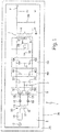
- the FIG. 1 shows a first embodiment of a high frequency amplifier arrangement 1.
- the high frequency amplifier arrangement 1 comprises a printed circuit board 2, on which an assembly 3 is arranged.
- the printed circuit board 2 may be a multilayer printed circuit board.
- the module 3 has two transistors S1, S2 in the form of LDMOS transistors, which are of similar design and whose source terminal is connected to a ground connection point 5 in each case.
- the assembly 3 may be arranged on a substrate.
- the assembly 3 may be arranged in a housing.
- the housing of the module 3 can be arranged in a through-hole in the printed circuit board 2.
- the connections of the module 3 can be contacted on the printed circuit board 2.
- the transistors S1, S2 are each connected to one end of a primary winding 6 of a power transformer 7, which is part of an output network.
- the secondary winding 4 of the power transformer 7 is connected to a ground 8 and the other with a high-frequency output 9.
- the sources of the transistors S1, S2 are connected via a respective capacitor 32, 33 to ground. This connection takes place via a plated-through hole in the heat distributor of the transistors S1, S2.
- the high-frequency amplifier arrangement 1 furthermore has a signal transmitter 10, which has a primary winding 11 which is connected, for example, via a matching network 18 to a high-frequency input 12.
- the secondary winding 13 of the signal transformer 10 is connected to the one via a resistive element 14, in particular a resistor, to the gate terminal 15 of the transistor S1.
- the secondary winding 13 is connected via a resistive element 16, in particular a resistor, to the gate terminal 17 of the transistor S2.
- the resistive elements 14, 16 and the secondary winding 13 are thus connected in series.
- the signal transmitter 10 is also arranged on the circuit board 2, as well as the power transformer. 7
- the printed circuit board 2 lies flat on a cooling plate 25, which is also connected to ground 26.
- the assembly 3 may be mounted on a copper plate for cooling.
- the copper plate can be used for heat transfer from the assembly 3 to the cooling plate 25, and in particular for heat spreading.
- the copper plate may be arranged in the same through-hole in the printed circuit board 2, as the assembly 3.
- the copper plate may have a larger area than the The through-hole may be configured in stages, adapted to the surfaces of the copper plate and the assembly 3.
- FIG. 1 shows further that parallel to the primary winding 6 of the power transformer 7, a capacitor 35 is provided. Parallel to the secondary winding 4 of the power transformer 7, a capacitor 36 is also provided.
- the primary winding 6 of the power transformer 7 has a center tap 37, which serves for DC supply of the transistors S1, S2.
- a network 38 is connected, which may have an inductance and / or a capacitor.
- a series connection of a capacitor and an inductor can be provided.
- a capacitance to ground and a series inductance could be provided.
- the drains or collectors of the transistors S1, S2 are connected by a series circuit 40, comprising an inductance 41 and a capacitor 42.
- This series circuit 40 serves as a low-impedance termination of the third harmonic.
- a matching network 43 may further be provided, which has two capacitors 44, 45 whose connection point is connected to ground.
- the primary winding 6 of the power transformer 7 can be tuned.
- FIG. 2 shows the power transformer 7.
- the primary winding 6 is disposed below the secondary winding 4.
- the primary winding 6 has one turn, while the secondary winding 4 has two turns.
- the primary winding 6 and the secondary winding 4 take in about the same area.
- the extension in the x-direction and in the y-direction, ie in the longitudinal direction and in the transverse direction of the printed circuit board 2, is in each case less than ⁇ / 30, where ⁇ is the wavelength of the high-frequency signal to be generated.
- the primary winding 6 has a center tap 37 (the center tap 37 is not connected to the secondary winding 4, which is apparent from FIG Fig. 2 may not be so obvious).
- Both the primary winding 6 and the secondary winding 4 are arranged in upper layers of the printed circuit board. In particular, they are arranged above a lower layer 50 of the printed circuit board. Of the FIG. 2 it can also be seen that the primary winding 6 and the secondary winding 4 are each formed of conductor tracks. In the FIG. 2 Furthermore, the planar inductance 41 can be seen, which is likewise arranged in a position of the printed circuit board 2, but is located above the layer 50.
- FIG. 3 shows a sectional view through a printed circuit board 2.
- connecting pads 60 are provided for the connection of discrete components. Corresponding connection pads could also be on the layer 62.
- the lowest layer 50 of the printed circuit board 2 is formed metallic and flat. It represents a ground plate and is connected over a large area with a cooling plate 25.
- the primary winding 6 and the secondary winding 4 are arranged in upper layers 61, 62 of the circuit board.
- the distance b between the primary winding 6 and the secondary winding 4 is preferably less than half the width c of a conductor track of the primary winding 6 or the secondary winding 4.
- the distance d from the primary winding 6 to the layer 50 and also the distance e from the secondary winding. 4 the position 50 is greater than the distance b.
- connecting lines and also the planar inductance 41 may be provided.
- the FIG. 4 shows a voltage waveform 100 which is nearly semi-sinusoidal and a current waveform 101 which is substantially rectangular.
- the voltage or current waveforms 100, 101 turn on the transistors S1, S2, when the high-frequency amplifier arrangement 1 is tuned correctly. It can be seen that the voltage waveform 100 and the current waveform 101 overlap only slightly, with the result that in the transistors S1, S2 only a small heat output is generated.
Landscapes
- Engineering & Computer Science (AREA)
- Power Engineering (AREA)
- Microelectronics & Electronic Packaging (AREA)
- Physics & Mathematics (AREA)
- Plasma & Fusion (AREA)
- Chemical & Material Sciences (AREA)
- Analytical Chemistry (AREA)
- Amplifiers (AREA)
Applications Claiming Priority (3)
| Application Number | Priority Date | Filing Date | Title |
|---|---|---|---|
| DE102015212220.4A DE102015212220A1 (de) | 2015-06-30 | 2015-06-30 | Hochfrequenzverstärkeranordnung |
| PCT/EP2016/065385 WO2017001602A1 (fr) | 2015-06-30 | 2016-06-30 | Ensemble amplificateur haute fréquence |
| EP16740974.7A EP3317966B1 (fr) | 2015-06-30 | 2016-06-30 | Ensemble amplificateur haute fréquence |
Related Parent Applications (1)
| Application Number | Title | Priority Date | Filing Date |
|---|---|---|---|
| EP16740974.7A Division EP3317966B1 (fr) | 2015-06-30 | 2016-06-30 | Ensemble amplificateur haute fréquence |
Publications (3)
| Publication Number | Publication Date |
|---|---|
| EP3579409A1 true EP3579409A1 (fr) | 2019-12-11 |
| EP3579409B1 EP3579409B1 (fr) | 2023-11-08 |
| EP3579409C0 EP3579409C0 (fr) | 2023-11-08 |
Family
ID=56464173
Family Applications (2)
| Application Number | Title | Priority Date | Filing Date |
|---|---|---|---|
| EP19188920.3A Active EP3579409B1 (fr) | 2015-06-30 | 2016-06-30 | Dispositif amplificateur haute fréquence |
| EP16740974.7A Active EP3317966B1 (fr) | 2015-06-30 | 2016-06-30 | Ensemble amplificateur haute fréquence |
Family Applications After (1)
| Application Number | Title | Priority Date | Filing Date |
|---|---|---|---|
| EP16740974.7A Active EP3317966B1 (fr) | 2015-06-30 | 2016-06-30 | Ensemble amplificateur haute fréquence |
Country Status (7)
| Country | Link |
|---|---|
| US (1) | US10396720B2 (fr) |
| EP (2) | EP3579409B1 (fr) |
| JP (1) | JP6768015B2 (fr) |
| KR (2) | KR20230121937A (fr) |
| CN (1) | CN107735947B (fr) |
| DE (1) | DE102015212220A1 (fr) |
| WO (1) | WO2017001602A1 (fr) |
Families Citing this family (36)
| Publication number | Priority date | Publication date | Assignee | Title |
|---|---|---|---|---|
| DE102015212152B4 (de) * | 2015-06-30 | 2018-03-15 | TRUMPF Hüttinger GmbH + Co. KG | Nicht lineare Hochfrequenzverstärkeranordnung |
| DE102015212247A1 (de) * | 2015-06-30 | 2017-01-05 | TRUMPF Hüttinger GmbH + Co. KG | Hochfrequenzverstärkeranordnung |
| DE102015212220A1 (de) | 2015-06-30 | 2017-01-05 | TRUMPF Hüttinger GmbH + Co. KG | Hochfrequenzverstärkeranordnung |
| DE102017208917A1 (de) * | 2017-05-26 | 2018-11-29 | TRUMPF Hüttinger GmbH + Co. KG | Hochfrequenzverstärkeranordnung und Verfahren zur Auslegung einer Hochfrequenzverstärkeranordnung |
| WO2019102536A1 (fr) * | 2017-11-22 | 2019-05-31 | 株式会社Fuji | Dispositif d'alimentation électrique pour plasma, dispositif à plasma, et procédé de contrôle de dispositif d'alimentation électrique pour plasma |
| DE102018112639A1 (de) | 2018-05-25 | 2019-11-28 | Volkswagen Aktiengesellschaft | Kathodenanordnung und Verfahren zu deren Herstellung |
| DE102018112642A1 (de) | 2018-05-25 | 2019-11-28 | Volkswagen Aktiengesellschaft | Lithium-Ionen-Zelle und Verfahren zu deren Herstellung |
| DE102018112641A1 (de) | 2018-05-25 | 2019-11-28 | Volkswagen Aktiengesellschaft | Lithiumanode und Verfahren zu deren Herstellung |
| DE102018112637A1 (de) | 2018-05-25 | 2019-11-28 | Volkswagen Aktiengesellschaft | Lithiumanode und Verfahren zu deren Herstellung |
| WO2020094858A1 (fr) * | 2018-11-09 | 2020-05-14 | Koninklijke Philips N.V. | Amplificateur de puissance de radiofréquence et son procédé d'assemblage |
| EP3667350A1 (fr) * | 2018-12-13 | 2020-06-17 | Koninklijke Philips N.V. | Amplificateur d'alimentation de fréquence radio et procédé d'assemblage |
| GB2580155A (en) | 2018-12-21 | 2020-07-15 | Comet Ag | Radiofrequency power amplifier |
| JP7275624B2 (ja) * | 2019-02-13 | 2023-05-18 | 株式会社デンソー | 周波数帯域可変高周波増幅器 |
| US11004591B2 (en) * | 2019-04-17 | 2021-05-11 | Flex Ltd. | Multilayer transformer structure comprising multiple rectification elements |
| CN112444767B (zh) * | 2019-08-30 | 2024-12-03 | 通用电气精准医疗有限责任公司 | 用于磁共振成像的射频功率变换器和射频发射系统 |
| DE102020104090A1 (de) * | 2020-02-17 | 2021-08-19 | Comet Ag | Hochfrequenzverstärker-Anordnung für einen Hochfrequenzgenerator |
| JP2021175053A (ja) * | 2020-04-22 | 2021-11-01 | 株式会社村田製作所 | 高周波モジュールおよび通信装置 |
| CN115668759A (zh) * | 2020-05-25 | 2023-01-31 | 株式会社村田制作所 | 追踪器模块、功率放大模块、高频模块以及通信装置 |
| US11979974B1 (en) * | 2020-06-04 | 2024-05-07 | Inno-Hale Ltd | System and method for plasma generation of nitric oxide |
| WO2022163791A1 (fr) * | 2021-01-28 | 2022-08-04 | 株式会社村田製作所 | Module de suivi, module d'amplification de puissance, module haute fréquence et dispositif de communication |
| CN216162675U (zh) * | 2021-09-16 | 2022-04-01 | 深圳飞骧科技股份有限公司 | 一种差分功率放大器 |
| CN216390923U (zh) * | 2021-11-09 | 2022-04-26 | 深圳飞骧科技股份有限公司 | 射频功率放大器、射频芯片及无线通讯设备 |
| CN118302953A (zh) * | 2021-12-07 | 2024-07-05 | 株式会社村田制作所 | 功率放大电路、功率放大装置以及阻抗匹配装置 |
| KR102786539B1 (ko) * | 2022-02-25 | 2025-03-26 | 경상국립대학교산학협력단 | 저왜율 고출력을 지원하는 전력 증폭기 |
| KR102744917B1 (ko) * | 2022-02-25 | 2024-12-19 | 경상국립대학교산학협력단 | 전력 증폭기의 출력을 제어하기 위한 장치 |
| DE102023104958A1 (de) * | 2023-02-28 | 2024-08-29 | TRUMPF Hüttinger GmbH + Co. KG | Impedanzanpassungsbaustein, Impedanzanpassungsschaltung, Plasmaprozessversorgungssystem und Plasmaprozesssystem |
| JP7651638B1 (ja) | 2023-09-12 | 2025-03-26 | 株式会社京三製作所 | スイッチング増幅器 |
| DE102023129490A1 (de) | 2023-10-25 | 2025-04-30 | TRUMPF Hüttinger GmbH + Co. KG | Hochfrequenzverstärkeranordnung |
| DE102023131882A1 (de) | 2023-11-15 | 2025-05-15 | TRUMPF Hüttinger GmbH + Co. KG | Kühlanordnung, Elektronikbaugruppe, elektrischer Leistungsumwandler und Verfahren zu deren Zusammenbau |
| WO2025104320A1 (fr) | 2023-11-15 | 2025-05-22 | TRUMPF Hüttinger GmbH + Co. KG | Module structurale électronique de puissance avec refroidissement et convertisseur de puissance |
| DE102023131878A1 (de) | 2023-11-15 | 2025-05-15 | TRUMPF Hüttinger GmbH + Co. KG | Leistungselektronische Baueinheit mit Kühlung und Leistungsumwandler |
| DE102023131877A1 (de) | 2023-11-15 | 2025-05-15 | TRUMPF Hüttinger GmbH + Co. KG | Leistungselektronische Baueinheit mit Kühlung und Leistungsumwandler |
| DE102023132074A1 (de) | 2023-11-17 | 2025-05-22 | TRUMPF Hüttinger GmbH + Co. KG | Leistungselektronische Baueinheit, Leistungswandleranordnung und Verfahren zum Zusammenbau mehrerer solcher Baueinheiten |
| DE102024102016A1 (de) | 2024-01-24 | 2025-07-24 | TRUMPF Hüttinger GmbH + Co. KG | Leistungsversorgungssystem zur Versorgung eines Plasma- oder Gaslaserprozesses und Verfahren zur Anregung eines Plasmas |
| DE102024108635B3 (de) | 2024-03-26 | 2025-08-07 | TRUMPF Hüttinger GmbH + Co. KG | Elektronische Vorrichtung mit integrierter Leistungsbaueinheit, Herstellungsverfahren sowie elektrischer Leistungsumwandler |
| DE102024114020A1 (de) | 2024-05-17 | 2025-11-20 | TRUMPF Hüttinger GmbH + Co. KG | Leistungsversorgungssystem zur Versorgung eines Plasma- oder Gaslaserprozesses und Verfahren zum Betrieb eines solchen Leistungsversorgungssystems |
Citations (13)
| Publication number | Priority date | Publication date | Assignee | Title |
|---|---|---|---|---|
| US5835367A (en) | 1998-01-20 | 1998-11-10 | Industrial Technology Research Institute | Distributed plannar-type high voltage transformer |
| US20030020583A1 (en) * | 2001-06-15 | 2003-01-30 | Hui Ron Shu Yuen | Planar printed-circuit-board transformers with effective electromagnetic interference (emi) shielding |
| US20070030659A1 (en) * | 2003-09-29 | 2007-02-08 | Yukiharu Suzuki | Multilayer laminated circuit board |
| CA2556839A1 (fr) * | 2005-08-23 | 2007-02-23 | Synergy Microwave Corporation | Symetriseur, melangeurs et amplificateurs de planificateur multicouche |
| US7221102B2 (en) | 2003-02-07 | 2007-05-22 | Daihen Corporation | High-frequency power supply device |
| US20080272875A1 (en) | 2005-08-04 | 2008-11-06 | Daquan Huang | "Interleaved Three-Dimensional On-Chip Differential Inductors and Transformers |
| US20090027936A1 (en) | 2007-07-23 | 2009-01-29 | Huettinger Elektronik Gmbh + Co. Kg | Rf power supply |
| JP4271457B2 (ja) * | 2003-02-07 | 2009-06-03 | 株式会社ダイヘン | 高周波電源装置 |
| US20100148866A1 (en) | 2007-01-10 | 2010-06-17 | Samsung Electro-Mechanics Company | Systems and Methods for Power Amplifiers with Voltage Boosting Multi-Primary Transformers |
| US7768371B2 (en) * | 1998-02-05 | 2010-08-03 | City University Of Hong Kong | Coreless printed-circuit-board (PCB) transformers and operating techniques therefor |
| US20110241781A1 (en) * | 2010-04-02 | 2011-10-06 | Mks Instruments, Inc. | Variable Class Characteristic Amplifier |
| US20130038226A1 (en) | 2010-03-11 | 2013-02-14 | Huettinger Elektronik Gmbh + Co. Kg | Plasma Supply Arrangement Having Quadrature Coupler |
| US20140361690A1 (en) * | 2011-12-27 | 2014-12-11 | Tokyo Electron Limited | Plasma processing apparatus |
Family Cites Families (16)
| Publication number | Priority date | Publication date | Assignee | Title |
|---|---|---|---|---|
| US4107728A (en) * | 1977-01-07 | 1978-08-15 | Varian Associates, Inc. | Package for push-pull semiconductor devices |
| US5015972A (en) | 1989-08-17 | 1991-05-14 | Motorola, Inc. | Broadband RF transformer |
| JP3055483B2 (ja) * | 1997-01-24 | 2000-06-26 | 日本電気株式会社 | 混成集積回路 |
| US6043607A (en) * | 1997-12-16 | 2000-03-28 | Applied Materials, Inc. | Apparatus for exciting a plasma in a semiconductor wafer processing system using a complex RF waveform |
| US7180758B2 (en) * | 1999-07-22 | 2007-02-20 | Mks Instruments, Inc. | Class E amplifier with inductive clamp |
| SE0004794L (sv) | 2000-12-22 | 2002-06-23 | Ericsson Telefon Ab L M | En flerskikts-symmetreringstransformatorstruktur |
| JP4772232B2 (ja) * | 2001-08-29 | 2011-09-14 | アジレント・テクノロジーズ・インク | 高周波増幅回路及び高周波増幅回路の駆動方法 |
| JP2005039799A (ja) * | 2003-06-26 | 2005-02-10 | Matsushita Electric Ind Co Ltd | 電力増幅器、電力分配器および電力合成器 |
| US6879209B2 (en) | 2003-07-08 | 2005-04-12 | Icefyre Semiconductor Corp. | Switched-mode power amplifier using lumped element impedance inverter for parallel combining |
| FR2876516A1 (fr) * | 2004-10-11 | 2006-04-14 | Thomson Licensing Sa | Amplificateur destine a generer un signal de tension rectangulaire a commutations douces sur une charge capacitive |
| US7486141B2 (en) * | 2005-12-21 | 2009-02-03 | Trex Enterprises Corp. | Wide bandwidth, high power amplifier |
| US7605673B2 (en) | 2006-06-02 | 2009-10-20 | Coherent, Inc. | Transformer for impedance-matching power output of RF amplifier to gas-laser discharge |
| CN101803184A (zh) * | 2007-09-21 | 2010-08-11 | 日本电气株式会社 | 大功率放大器,无线发射器,无线收发器以及用于安装大功率放大器的方法 |
| US8195109B2 (en) * | 2010-03-23 | 2012-06-05 | Texas Instruments Incorporated | Single ended switched power amplifier with tuned load coupling block |
| JP5829885B2 (ja) * | 2011-10-19 | 2015-12-09 | 株式会社Wave Technology | バラン |
| DE102015212220A1 (de) | 2015-06-30 | 2017-01-05 | TRUMPF Hüttinger GmbH + Co. KG | Hochfrequenzverstärkeranordnung |
-
2015
- 2015-06-30 DE DE102015212220.4A patent/DE102015212220A1/de not_active Withdrawn
-
2016
- 2016-06-30 WO PCT/EP2016/065385 patent/WO2017001602A1/fr not_active Ceased
- 2016-06-30 EP EP19188920.3A patent/EP3579409B1/fr active Active
- 2016-06-30 JP JP2017568163A patent/JP6768015B2/ja active Active
- 2016-06-30 KR KR1020237027126A patent/KR20230121937A/ko not_active Ceased
- 2016-06-30 KR KR1020187001429A patent/KR20180021801A/ko not_active Ceased
- 2016-06-30 EP EP16740974.7A patent/EP3317966B1/fr active Active
- 2016-06-30 CN CN201680038821.1A patent/CN107735947B/zh active Active
-
2017
- 2017-12-27 US US15/855,584 patent/US10396720B2/en active Active
Patent Citations (13)
| Publication number | Priority date | Publication date | Assignee | Title |
|---|---|---|---|---|
| US5835367A (en) | 1998-01-20 | 1998-11-10 | Industrial Technology Research Institute | Distributed plannar-type high voltage transformer |
| US7768371B2 (en) * | 1998-02-05 | 2010-08-03 | City University Of Hong Kong | Coreless printed-circuit-board (PCB) transformers and operating techniques therefor |
| US20030020583A1 (en) * | 2001-06-15 | 2003-01-30 | Hui Ron Shu Yuen | Planar printed-circuit-board transformers with effective electromagnetic interference (emi) shielding |
| JP4271457B2 (ja) * | 2003-02-07 | 2009-06-03 | 株式会社ダイヘン | 高周波電源装置 |
| US7221102B2 (en) | 2003-02-07 | 2007-05-22 | Daihen Corporation | High-frequency power supply device |
| US20070030659A1 (en) * | 2003-09-29 | 2007-02-08 | Yukiharu Suzuki | Multilayer laminated circuit board |
| US20080272875A1 (en) | 2005-08-04 | 2008-11-06 | Daquan Huang | "Interleaved Three-Dimensional On-Chip Differential Inductors and Transformers |
| CA2556839A1 (fr) * | 2005-08-23 | 2007-02-23 | Synergy Microwave Corporation | Symetriseur, melangeurs et amplificateurs de planificateur multicouche |
| US20100148866A1 (en) | 2007-01-10 | 2010-06-17 | Samsung Electro-Mechanics Company | Systems and Methods for Power Amplifiers with Voltage Boosting Multi-Primary Transformers |
| US20090027936A1 (en) | 2007-07-23 | 2009-01-29 | Huettinger Elektronik Gmbh + Co. Kg | Rf power supply |
| US20130038226A1 (en) | 2010-03-11 | 2013-02-14 | Huettinger Elektronik Gmbh + Co. Kg | Plasma Supply Arrangement Having Quadrature Coupler |
| US20110241781A1 (en) * | 2010-04-02 | 2011-10-06 | Mks Instruments, Inc. | Variable Class Characteristic Amplifier |
| US20140361690A1 (en) * | 2011-12-27 | 2014-12-11 | Tokyo Electron Limited | Plasma processing apparatus |
Non-Patent Citations (6)
| Title |
|---|
| CONCETTINA BUCCELLA ET AL: "A computational method of temperature distribution in high frequency planar transformers", INDUSTRIAL ELECTRONICS (ISIE), 2011 IEEE INTERNATIONAL SYMPOSIUM ON, IEEE, 27 June 2011 (2011-06-27), pages 477 - 482, XP032019032, ISBN: 978-1-4244-9310-4, DOI: 10.1109/ISIE.2011.5984072 * |
| FREDERICK H RAAB ED - ANONYMOUS: "Broadband Class-E Power Amplifier for HF and VHF", MICROWAVE SYMPOSIUM DIGEST, 2006. IEEE MTT-S INTERNATIONAL, IEEE, PI, 1 June 2006 (2006-06-01), pages 902 - 905, XP031018618, ISBN: 978-0-7803-9541-1 * |
| JAWAD SALEEM ET AL: "High frequency full bridge converter using multilayer coreless printed circuit board step up power transformer", CIRCUIT THEORY AND DESIGN (ECCTD), 2011 20TH EUROPEAN CONFERENCE ON, IEEE, 29 August 2011 (2011-08-29), pages 805 - 808, XP031975687, ISBN: 978-1-4577-0617-2, DOI: 10.1109/ECCTD.2011.6043837 * |
| MAJID A ET AL: "High frequency half-bridge converter using multilayered coreless Printed Circuit Board step-down power transformer", POWER ELECTRONICS AND ECCE ASIA (ICPE&ECCE), 2011 IEEE 8TH INTERNATIONAL CONFERENCE ON, IEEE, 30 May 2011 (2011-05-30), pages 1177 - 1181, XP031956308, ISBN: 978-1-61284-958-4, DOI: 10.1109/ICPE.2011.5944712 * |
| SCHAUWERS J-P ET AL: "Planar transformer technology applied to AC/DC conversion", TELECOMMUNICATION ENERGY CONFERENCE, 1999. INTELEC '99. THE 21ST INTER NATIONAL COPENHAGEN, DENMARK 6-9 JUNE 1999, PISCATAWAY, NJ, USA,IEEE, US, 6 June 1999 (1999-06-06), pages 5pp, XP010351421, ISBN: 978-0-7803-5624-5 * |
| WANG Y A ET AL: "Design of a planar power transformer for high voltage, high frequency use", TRANSMISSION AND DISTRIBUTION CONFERENCE AND EXPOSITION, 2010 IEEE PES, IEEE, PISCATAWAY, NJ, USA, 19 April 2010 (2010-04-19), pages 1 - 6, XP031689148, ISBN: 978-1-4244-6546-0 * |
Also Published As
| Publication number | Publication date |
|---|---|
| JP2018519758A (ja) | 2018-07-19 |
| EP3579409B1 (fr) | 2023-11-08 |
| WO2017001602A1 (fr) | 2017-01-05 |
| KR20230121937A (ko) | 2023-08-21 |
| CN107735947B (zh) | 2021-09-28 |
| JP6768015B2 (ja) | 2020-10-14 |
| CN107735947A (zh) | 2018-02-23 |
| EP3317966B1 (fr) | 2019-08-07 |
| US10396720B2 (en) | 2019-08-27 |
| US20180123526A1 (en) | 2018-05-03 |
| DE102015212220A1 (de) | 2017-01-05 |
| EP3317966A1 (fr) | 2018-05-09 |
| KR20180021801A (ko) | 2018-03-05 |
| EP3579409C0 (fr) | 2023-11-08 |
Similar Documents
| Publication | Publication Date | Title |
|---|---|---|
| EP3317966B1 (fr) | Ensemble amplificateur haute fréquence | |
| EP1701376B1 (fr) | Generateur de plasma sous vide | |
| EP3317965B1 (fr) | Ensemble amplificateur haute fréquence non linéaire | |
| DE202020103539U1 (de) | Schaltbare-Reaktanz-Einheit, veränderbare Reaktanz, Hochfrequenzgenerator und Impedanzanpassungsanordnung mit einer Schaltbare-Reaktanz- Einheit | |
| WO2003077414A2 (fr) | Amplificateur de puissance | |
| DE102008051630A1 (de) | Hochfrequenzleistungsverstärker | |
| WO2008014957A1 (fr) | Installation de circuit monolithique intégrable | |
| DE102016201244B4 (de) | Induktiv gekoppelter transformator mit abstimmbarem impedanzanpassungsnetzwerk | |
| DE112004001614B4 (de) | 90° Hybrid | |
| EP1699107B1 (fr) | Coupleur 3dB | |
| DE202010016850U1 (de) | HF Leistungs-Koppler | |
| DE102023104955A1 (de) | Impedanzanpassungsschaltung für ein Plasmaprozesssystem und ein Plasmaprozesssystem mit einer solchen Impedanzanpassungsschaltung | |
| DE102008027422B4 (de) | Integrierte Schaltung mit mehrstufiger Anpassungsschaltung und Verfahren zum Herstellen einer integrierten Schaltung mit mehrstufiger Anpassungsschaltung | |
| WO2025087982A1 (fr) | Agencement d'amplificateur haute fréquence | |
| EP3631980B1 (fr) | Ensemble amplificateur à haute fréquence et procédé pour configurer un ensemble amplificateur à haute fréquence | |
| DE102011086557A1 (de) | Koppleranordnung | |
| DE102011012622A1 (de) | Hochfrequenzleistungsvervielfacherlösung | |
| DE60304172T2 (de) | Modul zur entkopplung von hochfrequenz-signalen von einer versorgungsleitung | |
| DE102013111433A1 (de) | Planare symmetrische Spule für integrierte HF-Schaltungen | |
| AT413171B (de) | Halbleiter-bauelement mit einer kühlplatte | |
| DE102017200255A1 (de) | Leistungsverstärker | |
| EP3729645B1 (fr) | Arrangement d'un filtre lc, dispositif electrique ou electronique comprenant un arrangement d'un tel filtre lc | |
| DE102012213324A1 (de) | Anordnung mit DGS-Struktur für Hochfrequenzanwendungen | |
| EP3891886B1 (fr) | Transistor de puissance haute fréquence et amplificateur de puissance haute fréquence | |
| DE3238806A1 (de) | Symmetriereinrichtung |
Legal Events
| Date | Code | Title | Description |
|---|---|---|---|
| PUAI | Public reference made under article 153(3) epc to a published international application that has entered the european phase |
Free format text: ORIGINAL CODE: 0009012 |
|
| STAA | Information on the status of an ep patent application or granted ep patent |
Free format text: STATUS: THE APPLICATION HAS BEEN PUBLISHED |
|
| AC | Divisional application: reference to earlier application |
Ref document number: 3317966 Country of ref document: EP Kind code of ref document: P |
|
| AK | Designated contracting states |
Kind code of ref document: A1 Designated state(s): AL AT BE BG CH CY CZ DE DK EE ES FI FR GB GR HR HU IE IS IT LI LT LU LV MC MK MT NL NO PL PT RO RS SE SI SK SM TR |
|
| STAA | Information on the status of an ep patent application or granted ep patent |
Free format text: STATUS: REQUEST FOR EXAMINATION WAS MADE |
|
| 17P | Request for examination filed |
Effective date: 20200605 |
|
| RBV | Designated contracting states (corrected) |
Designated state(s): AL AT BE BG CH CY CZ DE DK EE ES FI FR GB GR HR HU IE IS IT LI LT LU LV MC MK MT NL NO PL PT RO RS SE SI SK SM TR |
|
| STAA | Information on the status of an ep patent application or granted ep patent |
Free format text: STATUS: EXAMINATION IS IN PROGRESS |
|
| 17Q | First examination report despatched |
Effective date: 20200828 |
|
| GRAP | Despatch of communication of intention to grant a patent |
Free format text: ORIGINAL CODE: EPIDOSNIGR1 |
|
| STAA | Information on the status of an ep patent application or granted ep patent |
Free format text: STATUS: GRANT OF PATENT IS INTENDED |
|
| INTG | Intention to grant announced |
Effective date: 20230602 |
|
| GRAS | Grant fee paid |
Free format text: ORIGINAL CODE: EPIDOSNIGR3 |
|
| GRAA | (expected) grant |
Free format text: ORIGINAL CODE: 0009210 |
|
| STAA | Information on the status of an ep patent application or granted ep patent |
Free format text: STATUS: THE PATENT HAS BEEN GRANTED |
|
| AC | Divisional application: reference to earlier application |
Ref document number: 3317966 Country of ref document: EP Kind code of ref document: P |
|
| AK | Designated contracting states |
Kind code of ref document: B1 Designated state(s): AL AT BE BG CH CY CZ DE DK EE ES FI FR GB GR HR HU IE IS IT LI LT LU LV MC MK MT NL NO PL PT RO RS SE SI SK SM TR |
|
| REG | Reference to a national code |
Ref country code: GB Ref legal event code: FG4D Free format text: NOT ENGLISH |
|
| REG | Reference to a national code |
Ref country code: CH Ref legal event code: EP |
|
| REG | Reference to a national code |
Ref country code: DE Ref legal event code: R096 Ref document number: 502016016213 Country of ref document: DE |
|
| REG | Reference to a national code |
Ref country code: IE Ref legal event code: FG4D Free format text: LANGUAGE OF EP DOCUMENT: GERMAN |
|
| U01 | Request for unitary effect filed |
Effective date: 20231206 |
|
| U07 | Unitary effect registered |
Designated state(s): AT BE BG DE DK EE FI FR IT LT LU LV MT NL PT SE SI Effective date: 20231212 |
|
| PG25 | Lapsed in a contracting state [announced via postgrant information from national office to epo] |
Ref country code: GR Free format text: LAPSE BECAUSE OF FAILURE TO SUBMIT A TRANSLATION OF THE DESCRIPTION OR TO PAY THE FEE WITHIN THE PRESCRIBED TIME-LIMIT Effective date: 20240209 |
|
| PG25 | Lapsed in a contracting state [announced via postgrant information from national office to epo] |
Ref country code: IS Free format text: LAPSE BECAUSE OF FAILURE TO SUBMIT A TRANSLATION OF THE DESCRIPTION OR TO PAY THE FEE WITHIN THE PRESCRIBED TIME-LIMIT Effective date: 20240308 |
|
| PG25 | Lapsed in a contracting state [announced via postgrant information from national office to epo] |
Ref country code: ES Free format text: LAPSE BECAUSE OF FAILURE TO SUBMIT A TRANSLATION OF THE DESCRIPTION OR TO PAY THE FEE WITHIN THE PRESCRIBED TIME-LIMIT Effective date: 20231108 |
|
| PG25 | Lapsed in a contracting state [announced via postgrant information from national office to epo] |
Ref country code: IS Free format text: LAPSE BECAUSE OF FAILURE TO SUBMIT A TRANSLATION OF THE DESCRIPTION OR TO PAY THE FEE WITHIN THE PRESCRIBED TIME-LIMIT Effective date: 20240308 Ref country code: GR Free format text: LAPSE BECAUSE OF FAILURE TO SUBMIT A TRANSLATION OF THE DESCRIPTION OR TO PAY THE FEE WITHIN THE PRESCRIBED TIME-LIMIT Effective date: 20240209 Ref country code: ES Free format text: LAPSE BECAUSE OF FAILURE TO SUBMIT A TRANSLATION OF THE DESCRIPTION OR TO PAY THE FEE WITHIN THE PRESCRIBED TIME-LIMIT Effective date: 20231108 |
|
| PG25 | Lapsed in a contracting state [announced via postgrant information from national office to epo] |
Ref country code: RS Free format text: LAPSE BECAUSE OF FAILURE TO SUBMIT A TRANSLATION OF THE DESCRIPTION OR TO PAY THE FEE WITHIN THE PRESCRIBED TIME-LIMIT Effective date: 20231108 Ref country code: PL Free format text: LAPSE BECAUSE OF FAILURE TO SUBMIT A TRANSLATION OF THE DESCRIPTION OR TO PAY THE FEE WITHIN THE PRESCRIBED TIME-LIMIT Effective date: 20231108 Ref country code: NO Free format text: LAPSE BECAUSE OF FAILURE TO SUBMIT A TRANSLATION OF THE DESCRIPTION OR TO PAY THE FEE WITHIN THE PRESCRIBED TIME-LIMIT Effective date: 20240208 Ref country code: HR Free format text: LAPSE BECAUSE OF FAILURE TO SUBMIT A TRANSLATION OF THE DESCRIPTION OR TO PAY THE FEE WITHIN THE PRESCRIBED TIME-LIMIT Effective date: 20231108 |
|
| PG25 | Lapsed in a contracting state [announced via postgrant information from national office to epo] |
Ref country code: CZ Free format text: LAPSE BECAUSE OF FAILURE TO SUBMIT A TRANSLATION OF THE DESCRIPTION OR TO PAY THE FEE WITHIN THE PRESCRIBED TIME-LIMIT Effective date: 20231108 |
|
| PG25 | Lapsed in a contracting state [announced via postgrant information from national office to epo] |
Ref country code: SK Free format text: LAPSE BECAUSE OF FAILURE TO SUBMIT A TRANSLATION OF THE DESCRIPTION OR TO PAY THE FEE WITHIN THE PRESCRIBED TIME-LIMIT Effective date: 20231108 |
|
| PG25 | Lapsed in a contracting state [announced via postgrant information from national office to epo] |
Ref country code: SM Free format text: LAPSE BECAUSE OF FAILURE TO SUBMIT A TRANSLATION OF THE DESCRIPTION OR TO PAY THE FEE WITHIN THE PRESCRIBED TIME-LIMIT Effective date: 20231108 Ref country code: SK Free format text: LAPSE BECAUSE OF FAILURE TO SUBMIT A TRANSLATION OF THE DESCRIPTION OR TO PAY THE FEE WITHIN THE PRESCRIBED TIME-LIMIT Effective date: 20231108 Ref country code: RO Free format text: LAPSE BECAUSE OF FAILURE TO SUBMIT A TRANSLATION OF THE DESCRIPTION OR TO PAY THE FEE WITHIN THE PRESCRIBED TIME-LIMIT Effective date: 20231108 Ref country code: CZ Free format text: LAPSE BECAUSE OF FAILURE TO SUBMIT A TRANSLATION OF THE DESCRIPTION OR TO PAY THE FEE WITHIN THE PRESCRIBED TIME-LIMIT Effective date: 20231108 |
|
| U20 | Renewal fee for the european patent with unitary effect paid |
Year of fee payment: 9 Effective date: 20240625 |
|
| REG | Reference to a national code |
Ref country code: DE Ref legal event code: R097 Ref document number: 502016016213 Country of ref document: DE |
|
| PLBE | No opposition filed within time limit |
Free format text: ORIGINAL CODE: 0009261 |
|
| STAA | Information on the status of an ep patent application or granted ep patent |
Free format text: STATUS: NO OPPOSITION FILED WITHIN TIME LIMIT |
|
| 26N | No opposition filed |
Effective date: 20240809 |
|
| PG25 | Lapsed in a contracting state [announced via postgrant information from national office to epo] |
Ref country code: MC Free format text: LAPSE BECAUSE OF FAILURE TO SUBMIT A TRANSLATION OF THE DESCRIPTION OR TO PAY THE FEE WITHIN THE PRESCRIBED TIME-LIMIT Effective date: 20231108 |
|
| PG25 | Lapsed in a contracting state [announced via postgrant information from national office to epo] |
Ref country code: IE Free format text: LAPSE BECAUSE OF NON-PAYMENT OF DUE FEES Effective date: 20240630 |
|
| PGFP | Annual fee paid to national office [announced via postgrant information from national office to epo] |
Ref country code: GB Payment date: 20250618 Year of fee payment: 10 |
|
| U20 | Renewal fee for the european patent with unitary effect paid |
Year of fee payment: 10 Effective date: 20250627 |
|
| PGFP | Annual fee paid to national office [announced via postgrant information from national office to epo] |
Ref country code: CH Payment date: 20250701 Year of fee payment: 10 |
|
| PG25 | Lapsed in a contracting state [announced via postgrant information from national office to epo] |
Ref country code: CY Free format text: LAPSE BECAUSE OF FAILURE TO SUBMIT A TRANSLATION OF THE DESCRIPTION OR TO PAY THE FEE WITHIN THE PRESCRIBED TIME-LIMIT; INVALID AB INITIO Effective date: 20160630 |
|
| PG25 | Lapsed in a contracting state [announced via postgrant information from national office to epo] |
Ref country code: HU Free format text: LAPSE BECAUSE OF FAILURE TO SUBMIT A TRANSLATION OF THE DESCRIPTION OR TO PAY THE FEE WITHIN THE PRESCRIBED TIME-LIMIT; INVALID AB INITIO Effective date: 20160630 |