EP3581995B1 - Dispositif d'affichage d'image - Google Patents
Dispositif d'affichage d'image Download PDFInfo
- Publication number
- EP3581995B1 EP3581995B1 EP18750651.4A EP18750651A EP3581995B1 EP 3581995 B1 EP3581995 B1 EP 3581995B1 EP 18750651 A EP18750651 A EP 18750651A EP 3581995 B1 EP3581995 B1 EP 3581995B1
- Authority
- EP
- European Patent Office
- Prior art keywords
- luminance
- support pins
- sheet
- image display
- outer edge
- Prior art date
- Legal status (The legal status is an assumption and is not a legal conclusion. Google has not performed a legal analysis and makes no representation as to the accuracy of the status listed.)
- Active
Links
Images


Classifications
-
- G—PHYSICS
- G02—OPTICS
- G02F—OPTICAL DEVICES OR ARRANGEMENTS FOR THE CONTROL OF LIGHT BY MODIFICATION OF THE OPTICAL PROPERTIES OF THE MEDIA OF THE ELEMENTS INVOLVED THEREIN; NON-LINEAR OPTICS; FREQUENCY-CHANGING OF LIGHT; OPTICAL LOGIC ELEMENTS; OPTICAL ANALOGUE/DIGITAL CONVERTERS
- G02F1/00—Devices or arrangements for the control of the intensity, colour, phase, polarisation or direction of light arriving from an independent light source, e.g. switching, gating or modulating; Non-linear optics
- G02F1/01—Devices or arrangements for the control of the intensity, colour, phase, polarisation or direction of light arriving from an independent light source, e.g. switching, gating or modulating; Non-linear optics for the control of the intensity, phase, polarisation or colour
- G02F1/13—Devices or arrangements for the control of the intensity, colour, phase, polarisation or direction of light arriving from an independent light source, e.g. switching, gating or modulating; Non-linear optics for the control of the intensity, phase, polarisation or colour based on liquid crystals, e.g. single liquid crystal display cells
- G02F1/133—Constructional arrangements; Operation of liquid crystal cells; Circuit arrangements
- G02F1/1333—Constructional arrangements; Manufacturing methods
- G02F1/1335—Structural association of cells with optical devices, e.g. polarisers or reflectors
- G02F1/1336—Illuminating devices
- G02F1/133602—Direct backlight
- G02F1/133611—Direct backlight including means for improving the brightness uniformity
-
- F—MECHANICAL ENGINEERING; LIGHTING; HEATING; WEAPONS; BLASTING
- F21—LIGHTING
- F21S—NON-PORTABLE LIGHTING DEVICES; SYSTEMS THEREOF; VEHICLE LIGHTING DEVICES SPECIALLY ADAPTED FOR VEHICLE EXTERIORS
- F21S2/00—Systems of lighting devices, not provided for in main groups F21S4/00 - F21S10/00 or F21S19/00, e.g. of modular construction
-
- G—PHYSICS
- G02—OPTICS
- G02F—OPTICAL DEVICES OR ARRANGEMENTS FOR THE CONTROL OF LIGHT BY MODIFICATION OF THE OPTICAL PROPERTIES OF THE MEDIA OF THE ELEMENTS INVOLVED THEREIN; NON-LINEAR OPTICS; FREQUENCY-CHANGING OF LIGHT; OPTICAL LOGIC ELEMENTS; OPTICAL ANALOGUE/DIGITAL CONVERTERS
- G02F1/00—Devices or arrangements for the control of the intensity, colour, phase, polarisation or direction of light arriving from an independent light source, e.g. switching, gating or modulating; Non-linear optics
- G02F1/01—Devices or arrangements for the control of the intensity, colour, phase, polarisation or direction of light arriving from an independent light source, e.g. switching, gating or modulating; Non-linear optics for the control of the intensity, phase, polarisation or colour
- G02F1/13—Devices or arrangements for the control of the intensity, colour, phase, polarisation or direction of light arriving from an independent light source, e.g. switching, gating or modulating; Non-linear optics for the control of the intensity, phase, polarisation or colour based on liquid crystals, e.g. single liquid crystal display cells
- G02F1/133—Constructional arrangements; Operation of liquid crystal cells; Circuit arrangements
- G02F1/1333—Constructional arrangements; Manufacturing methods
-
- G—PHYSICS
- G02—OPTICS
- G02F—OPTICAL DEVICES OR ARRANGEMENTS FOR THE CONTROL OF LIGHT BY MODIFICATION OF THE OPTICAL PROPERTIES OF THE MEDIA OF THE ELEMENTS INVOLVED THEREIN; NON-LINEAR OPTICS; FREQUENCY-CHANGING OF LIGHT; OPTICAL LOGIC ELEMENTS; OPTICAL ANALOGUE/DIGITAL CONVERTERS
- G02F1/00—Devices or arrangements for the control of the intensity, colour, phase, polarisation or direction of light arriving from an independent light source, e.g. switching, gating or modulating; Non-linear optics
- G02F1/01—Devices or arrangements for the control of the intensity, colour, phase, polarisation or direction of light arriving from an independent light source, e.g. switching, gating or modulating; Non-linear optics for the control of the intensity, phase, polarisation or colour
- G02F1/13—Devices or arrangements for the control of the intensity, colour, phase, polarisation or direction of light arriving from an independent light source, e.g. switching, gating or modulating; Non-linear optics for the control of the intensity, phase, polarisation or colour based on liquid crystals, e.g. single liquid crystal display cells
- G02F1/133—Constructional arrangements; Operation of liquid crystal cells; Circuit arrangements
- G02F1/1333—Constructional arrangements; Manufacturing methods
- G02F1/133308—Support structures for LCD panels, e.g. frames or bezels
-
- G—PHYSICS
- G02—OPTICS
- G02F—OPTICAL DEVICES OR ARRANGEMENTS FOR THE CONTROL OF LIGHT BY MODIFICATION OF THE OPTICAL PROPERTIES OF THE MEDIA OF THE ELEMENTS INVOLVED THEREIN; NON-LINEAR OPTICS; FREQUENCY-CHANGING OF LIGHT; OPTICAL LOGIC ELEMENTS; OPTICAL ANALOGUE/DIGITAL CONVERTERS
- G02F1/00—Devices or arrangements for the control of the intensity, colour, phase, polarisation or direction of light arriving from an independent light source, e.g. switching, gating or modulating; Non-linear optics
- G02F1/01—Devices or arrangements for the control of the intensity, colour, phase, polarisation or direction of light arriving from an independent light source, e.g. switching, gating or modulating; Non-linear optics for the control of the intensity, phase, polarisation or colour
- G02F1/13—Devices or arrangements for the control of the intensity, colour, phase, polarisation or direction of light arriving from an independent light source, e.g. switching, gating or modulating; Non-linear optics for the control of the intensity, phase, polarisation or colour based on liquid crystals, e.g. single liquid crystal display cells
- G02F1/133—Constructional arrangements; Operation of liquid crystal cells; Circuit arrangements
- G02F1/1333—Constructional arrangements; Manufacturing methods
- G02F1/1335—Structural association of cells with optical devices, e.g. polarisers or reflectors
- G02F1/1336—Illuminating devices
- G02F1/133602—Direct backlight
-
- G—PHYSICS
- G02—OPTICS
- G02F—OPTICAL DEVICES OR ARRANGEMENTS FOR THE CONTROL OF LIGHT BY MODIFICATION OF THE OPTICAL PROPERTIES OF THE MEDIA OF THE ELEMENTS INVOLVED THEREIN; NON-LINEAR OPTICS; FREQUENCY-CHANGING OF LIGHT; OPTICAL LOGIC ELEMENTS; OPTICAL ANALOGUE/DIGITAL CONVERTERS
- G02F1/00—Devices or arrangements for the control of the intensity, colour, phase, polarisation or direction of light arriving from an independent light source, e.g. switching, gating or modulating; Non-linear optics
- G02F1/01—Devices or arrangements for the control of the intensity, colour, phase, polarisation or direction of light arriving from an independent light source, e.g. switching, gating or modulating; Non-linear optics for the control of the intensity, phase, polarisation or colour
- G02F1/13—Devices or arrangements for the control of the intensity, colour, phase, polarisation or direction of light arriving from an independent light source, e.g. switching, gating or modulating; Non-linear optics for the control of the intensity, phase, polarisation or colour based on liquid crystals, e.g. single liquid crystal display cells
- G02F1/133—Constructional arrangements; Operation of liquid crystal cells; Circuit arrangements
- G02F1/1333—Constructional arrangements; Manufacturing methods
- G02F1/1335—Structural association of cells with optical devices, e.g. polarisers or reflectors
- G02F1/1336—Illuminating devices
- G02F1/133602—Direct backlight
- G02F1/133605—Direct backlight including specially adapted reflectors
-
- G—PHYSICS
- G02—OPTICS
- G02F—OPTICAL DEVICES OR ARRANGEMENTS FOR THE CONTROL OF LIGHT BY MODIFICATION OF THE OPTICAL PROPERTIES OF THE MEDIA OF THE ELEMENTS INVOLVED THEREIN; NON-LINEAR OPTICS; FREQUENCY-CHANGING OF LIGHT; OPTICAL LOGIC ELEMENTS; OPTICAL ANALOGUE/DIGITAL CONVERTERS
- G02F1/00—Devices or arrangements for the control of the intensity, colour, phase, polarisation or direction of light arriving from an independent light source, e.g. switching, gating or modulating; Non-linear optics
- G02F1/01—Devices or arrangements for the control of the intensity, colour, phase, polarisation or direction of light arriving from an independent light source, e.g. switching, gating or modulating; Non-linear optics for the control of the intensity, phase, polarisation or colour
- G02F1/13—Devices or arrangements for the control of the intensity, colour, phase, polarisation or direction of light arriving from an independent light source, e.g. switching, gating or modulating; Non-linear optics for the control of the intensity, phase, polarisation or colour based on liquid crystals, e.g. single liquid crystal display cells
- G02F1/133—Constructional arrangements; Operation of liquid crystal cells; Circuit arrangements
- G02F1/1333—Constructional arrangements; Manufacturing methods
- G02F1/1335—Structural association of cells with optical devices, e.g. polarisers or reflectors
- G02F1/1336—Illuminating devices
- G02F1/133602—Direct backlight
- G02F1/133606—Direct backlight including a specially adapted diffusing, scattering or light controlling members
-
- G—PHYSICS
- G09—EDUCATION; CRYPTOGRAPHY; DISPLAY; ADVERTISING; SEALS
- G09F—DISPLAYING; ADVERTISING; SIGNS; LABELS OR NAME-PLATES; SEALS
- G09F9/00—Indicating arrangements for variable information in which the information is built-up on a support by selection or combination of individual elements
-
- G—PHYSICS
- G02—OPTICS
- G02F—OPTICAL DEVICES OR ARRANGEMENTS FOR THE CONTROL OF LIGHT BY MODIFICATION OF THE OPTICAL PROPERTIES OF THE MEDIA OF THE ELEMENTS INVOLVED THEREIN; NON-LINEAR OPTICS; FREQUENCY-CHANGING OF LIGHT; OPTICAL LOGIC ELEMENTS; OPTICAL ANALOGUE/DIGITAL CONVERTERS
- G02F1/00—Devices or arrangements for the control of the intensity, colour, phase, polarisation or direction of light arriving from an independent light source, e.g. switching, gating or modulating; Non-linear optics
- G02F1/01—Devices or arrangements for the control of the intensity, colour, phase, polarisation or direction of light arriving from an independent light source, e.g. switching, gating or modulating; Non-linear optics for the control of the intensity, phase, polarisation or colour
- G02F1/13—Devices or arrangements for the control of the intensity, colour, phase, polarisation or direction of light arriving from an independent light source, e.g. switching, gating or modulating; Non-linear optics for the control of the intensity, phase, polarisation or colour based on liquid crystals, e.g. single liquid crystal display cells
- G02F1/133—Constructional arrangements; Operation of liquid crystal cells; Circuit arrangements
- G02F1/1333—Constructional arrangements; Manufacturing methods
- G02F1/133308—Support structures for LCD panels, e.g. frames or bezels
- G02F1/133314—Back frames
-
- G—PHYSICS
- G02—OPTICS
- G02F—OPTICAL DEVICES OR ARRANGEMENTS FOR THE CONTROL OF LIGHT BY MODIFICATION OF THE OPTICAL PROPERTIES OF THE MEDIA OF THE ELEMENTS INVOLVED THEREIN; NON-LINEAR OPTICS; FREQUENCY-CHANGING OF LIGHT; OPTICAL LOGIC ELEMENTS; OPTICAL ANALOGUE/DIGITAL CONVERTERS
- G02F1/00—Devices or arrangements for the control of the intensity, colour, phase, polarisation or direction of light arriving from an independent light source, e.g. switching, gating or modulating; Non-linear optics
- G02F1/01—Devices or arrangements for the control of the intensity, colour, phase, polarisation or direction of light arriving from an independent light source, e.g. switching, gating or modulating; Non-linear optics for the control of the intensity, phase, polarisation or colour
- G02F1/13—Devices or arrangements for the control of the intensity, colour, phase, polarisation or direction of light arriving from an independent light source, e.g. switching, gating or modulating; Non-linear optics for the control of the intensity, phase, polarisation or colour based on liquid crystals, e.g. single liquid crystal display cells
- G02F1/133—Constructional arrangements; Operation of liquid crystal cells; Circuit arrangements
- G02F1/1333—Constructional arrangements; Manufacturing methods
- G02F1/1335—Structural association of cells with optical devices, e.g. polarisers or reflectors
- G02F1/1336—Illuminating devices
- G02F1/133602—Direct backlight
- G02F1/133603—Direct backlight with LEDs
-
- G—PHYSICS
- G02—OPTICS
- G02F—OPTICAL DEVICES OR ARRANGEMENTS FOR THE CONTROL OF LIGHT BY MODIFICATION OF THE OPTICAL PROPERTIES OF THE MEDIA OF THE ELEMENTS INVOLVED THEREIN; NON-LINEAR OPTICS; FREQUENCY-CHANGING OF LIGHT; OPTICAL LOGIC ELEMENTS; OPTICAL ANALOGUE/DIGITAL CONVERTERS
- G02F1/00—Devices or arrangements for the control of the intensity, colour, phase, polarisation or direction of light arriving from an independent light source, e.g. switching, gating or modulating; Non-linear optics
- G02F1/01—Devices or arrangements for the control of the intensity, colour, phase, polarisation or direction of light arriving from an independent light source, e.g. switching, gating or modulating; Non-linear optics for the control of the intensity, phase, polarisation or colour
- G02F1/13—Devices or arrangements for the control of the intensity, colour, phase, polarisation or direction of light arriving from an independent light source, e.g. switching, gating or modulating; Non-linear optics for the control of the intensity, phase, polarisation or colour based on liquid crystals, e.g. single liquid crystal display cells
- G02F1/133—Constructional arrangements; Operation of liquid crystal cells; Circuit arrangements
- G02F1/1333—Constructional arrangements; Manufacturing methods
- G02F1/1335—Structural association of cells with optical devices, e.g. polarisers or reflectors
- G02F1/1336—Illuminating devices
- G02F1/133602—Direct backlight
- G02F1/133608—Direct backlight including particular frames or supporting means
Definitions
- the present disclosure relates to image display apparatuses including a display panel such as a liquid crystal cell.
- Patent Literature (PTL) I discloses a display apparatus including, as a direct-lit backlight, a surface light source unit including a light-transmissive reflector for providing uniform surface illumination light having less luminance unevenness.
- EP 2 450 619 A1 relates to a lighting device having an LED, a chassis-side reflection sheet and sheet holding members.
- the present disclosure provides an image display apparatus that is thin in appearance and is capable of displaying an image with greater luminance uniformity throughout a screen.
- An image display apparatus in the present disclosure is thin in appearance and is capable of displaying an image with greater luminance uniformity throughout a screen.
- the inventors have found the following problem regarding conventional image display apparatuses.
- a display module circumferentially including a display panel is roughly a rectangular parallelepiped that is thin from front to back, and, to be more exact, has a shape with relatively broadly chamfered four sides on the back side of the display module.
- Such a shape of the display module in which the thickness is small at its end face produces a visual effect of making the display module itself look thinner than it is.
- the peripheral portion is smaller in thickness than the other portions.
- peripheral portion cannot employ a display mechanism common to the other portions due to the limitations of internal space in a thickness direction. For this reason, it is difficult to achieve uniform image quality throughout a screen. More specifically, image display apparatuses including a direct-lit backlight system may have difficulty in achieving uniform luminance from the center to periphery of the screen.
- the present disclosure has been made based on such an underlying knowledge, and the inventors have arrived, while responding to a demand for the above-described external appearance, at a concept for the structure of an image display apparatus that is capable of displaying an image with greater luminance uniformity throughout a screen.
- an up-down direction, a front-back direction, and a left-right direction of the image display apparatus correspond to the Y axis direction, the Z axis direction, and the X axis direction, respectively, in the following embodiments, these directional correspondences do not limit the orientation of the image display apparatus according to the present disclosure at the time of manufacture or use.
- FIG. 1 is an external perspective view of image display apparatus 10 according to the invention.
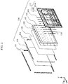
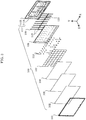
- FIG. 2 and FIG. 3 each are an exploded perspective view of liquid crystal module 100 according to the invention.
- Image display apparatus 10 is, for example, a liquid crystal television. As shown in FIG. 1 , image display apparatus 10 includes liquid crystal module 100, bezel 101, back cover 103, and stand 200.
- Liquid crystal module 100 is an image display module capable of displaying still and moving images, and includes display panel 102.
- display panel 102 is what is called a liquid crystal cell, and is a component in which liquid crystals are sealed between glass substrates. Display panel 102 is controlled according to an image signal inputted to image display apparatus 10 and thereby displays images.
- Liquid crystal module 100 can stand on a floor or table with stand 200. In this regard, however, liquid crystal module 100 may be hung on a wall, embedded in a wall, or suspended from a ceiling with other fittings instead of stand 200, for use as image display apparatus 10.
- Bezel 101 made of a resin is formed of parts corresponding to the respective four sides of image display apparatus 10, and the parts are joined to each other by, for example, screws. Bezel 101 and back cover 103 clamp together components therebetween, from display panel 102 to back frame 111, which will be described below.
- liquid crystal module 100 having the above configuration further includes molded frame 104, optical sheet unit 105, diffuser panel 106, luminance-equalizing sheet 107, reflective sheet 108, LED sheet 109, relay sheet 110, back frame 111, and support pins 112.
- Molded frame 104 and back frame 111 clamp together components (what is called a back light unit) therebetween, from optical sheet unit 105 to LED sheet 109 and relay sheet 110. It should be noted that FIG. 3 omits molded frame 104.
- Optical sheet unit 105 is configured by stacking two or three types of sheets having different optical properties.
- optical sheet unit 105 includes a vertical prism sheet, a horizontal prism sheet, and a diffuser sheet.
- Diffuser panel 106 diffusely emits, toward display panel 102, incident light from light-emitting diodes (LEDs) 113 that are disposed on LED sheet 109 and serve as light sources of image display apparatus 10.
- LEDs light-emitting diodes
- Luminance-equalizing sheet 107 increases a degree of uniformity of luminances of light (hereinafter also referred to as emitted light) from LEDs 113 on LED sheet 109 that differ from place to place, and transmits the light toward diffuser panel 106.
- Luminance-equalizing sheet 107 is, for example, a sheet-shaped component that is made of a resin such as polyethylene terephthalate (PET) densely containing microscopic bubbles and that has satisfactory light reflecting properties.
- PET polyethylene terephthalate
- Part of emitted light from LEDs 113 passes through these holes to an opposite side, that is, the side where diffuser panel 106 is present (also expressed as "light passes through luminance-equalizing sheet 107" in the present disclosure).
- the number, size, and distribution of the holes are adjusted so that luminance-equalizing sheet 107 equalizes amounts of transmission of light per unit area from light sources at a predetermined distance.
- luminance-equalizing sheet 107 smoothes the distribution characteristics of light emitted by each LED 113.
- the light from each LED 113, of which the distribution characteristics are smoothed by luminance-equalizing sheet 107 is diffused by diffuser panel 106 so that luminance unevenness is further reduced, and is emitted toward display panel 102.
- Reflective sheet 108 includes holes that correspond in location and size to respective LEDs 113 on LED sheet 109, and reflects light at the entire surface on a side facing a front surface of image display apparatus 10.
- Reflective sheet 108 includes: a flat portion that has a substantially flat surface smaller than an active area of display panel 102; and a side wall that rises from the ends of the four sides of the flat portion and reaches the outer edge of the active area of display panel 102 in a front view of image display apparatus 10.
- Reflective sheet 108 as a whole is substantially shaped to conform to back frame 111 to be described later.
- LED sheet 109 is a flexible printed board (hereinafter referred to as flexible printed circuits (FPCs)) on which LEDs 113 are mounted.
- FPCs flexible printed circuits
- LEDs 113 are mounted on one of two principal surfaces of the FPCs that are sheet-shaped, and a reflective layer that reflects light is disposed on the principal surface of the FPCs on which LEDs 113 are mounted, that is, the principal surface on the front side of image display apparatus 10.
- LEDs 113 on the principal surface of LED sheet 109 are arranged in rows and columns at substantially equal intervals so that LEDs 113 can illuminate as wide an area of the back surface of display panel 102 as possible while reducing unevenness depending on a location as much as possible.
- Relay sheet 110 is FPCs on which electrical paths for transmitting power, a control signal, or the like to each of LEDs 113 on LED sheet 109 are disposed. Further, like LED sheet 109, a reflective layer is disposed on a principal surface of relay sheet 110 on the front side of image display apparatus 10.
- Back frame 111 also referred to as a base plate, is a plate-shaped component made of a metal plate, and supports LED sheet 109 and relay sheet 110.
- Back frame 111 includes: flat portion 111A having a substantially flat surface smaller than an active area of display panel 102; and side wall 111B that rises from the outer edge of flat portion 111A, that is, the ends of the four sides, and reaches the outer edge of the active area of display panel 102 when image display apparatus 10 is seen from the front side (a side on which display panel 102 is present).
- back cover 103 is shaped to conform to the external shape of back frame 111, such a shape of liquid crystal module 100 in which the four sides on the back side of the rectangular parallelpiped that is thin from front to back (along the Z axis) are relatively broadly chamfered produces the above-described visual effect of making liquid crystal module 100 look thinner than it is.
- LEDs 113 which serve as the light sources, are disposed in flat portion 111A of back frame 111. More specifically, LED sheet 109 on which LEDs 113 are spaced substantially equally and relay sheet 110 are attached to flat portion 111A. Subsequently, reflective sheet 108 is further affixed to flat portion 111A so that LEDs 113 are exposed from the respective holes of reflective sheet 108. Emitted light from each LED 113 is directly incident on luminance-equalizing sheet 107 on the front side of image display apparatus 10, or is reflected by the reflective layer on the FPCs and reflective sheet 108 and then incident on luminance-equalizing sheet 107. Back frame 111 and molded frame 104 clamp together the back light unit therebetween, from optical sheet unit 105 to LED sheet 109 and relay sheet 110.
- Back frame 111 may further include a configuration for supporting each component of the back light unit.
- back frame 111 may include a cut and raised portion for hanging optical sheet unit 105, in the neighborhood of one side that is on the top side when image display apparatus 10 is placed for use.
- optical sheet unit 105 includes, for example, a tab having a hole for hooking on the cut and raised portion.
- Support pins 112 shown in FIG. 3 are pillar-shaped components. Each of support pins 112 includes: an end to be attached to back frame 111; tip 112A that is an end opposite to the end; and flange 112B that is flanged and at a longitudinally intermediate position on the pillar shape.
- Support pins 112 are attached to flat portion 111A of back frame 111 with reflective sheet 108 in between, and support pins 112 and back frame 111 clamp together reflective sheet 108.
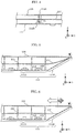
- FIG. 4 is a schematic cross-sectional view of a state in which support pin 112 attached to back frame 111 inside liquid crystal module 100 supports diffuser panel 106 and luminance-equalizing sheet 107. In this regard, however, among the components of liquid crystal module 100, those unnecessary for the illustration are omitted from FIG. 4 .
- Luminance-equalizing sheet 107 includes, in positions corresponding to respective support pins 112 attached to back frame 111, holes into which support pins 112 are inserted. After tip 112A of support pin 112 is inserted into the hole, luminance-equalizing sheet 107 is supported by flange 112B of support pin 112 as shown in FIG. 4 .
- support pin 112 may support luminance-equalizing sheet 107 at the longitudinally intermediate position that is designed to be at a certain appropriate distance from back frame 111 or LED 113, and this supporting configuration is not limited to flange 112B that is flanged.
- support pin 112 may include a portion like a pedestal having a top surface instead of flange 112B, and support luminance-equalizing sheet 107 with the top surface of the portion.
- support pin 112 may include a portion that gets thicker from the front to back of liquid crystal module 100 as installed, and support luminance-equalizing sheet 107 at a location in the portion where the portion and the hole of luminance-equalizing sheet 107 fit in diameter.
- Diffuser panel 106 is supported by an end of side wall 111B of back frame 111 in the periphery, and is supported by tip 112A of support pin 112 standing on flat portion 111A of back frame 111 in a portion other than the periphery as shown in FIG. 4 .
- support pins 112 are arranged in rows and columns at substantially equal intervals in flat portion 111A so that support pins 112 support the entirety of diffuser panel 106 and luminance-equalizing sheet 107.
- support pins 112 are arranged in positions away from respective LEDs 113, e.g. on lines each of which passes through equidistant points between horizontally or vertically adjacent two of LEDs 113, in order that support pins 112 do not block light toward luminance-equalizing sheet 107 as much as possible.
- liquid crystal module 100 for further increasing luminance uniformity throughout the screen, in such image display apparatus 10 according to the present disclosure.
- FIG. 5 is a schematic cross-sectional view of a configuration of liquid crystal module 100 according to example 1.
- FIG. 5 shows a cross section of part of liquid crystal module 100 which includes a portion extending from flat portion 111A to the upper part of side wall 111B of back frame 111.
- the configuration of liquid crystal module 100 is common to a portion extending from flat portion 111A to the lower part, right part, or left part of side wall 111B.
- FIG. 6 is a schematic cross-sectional view of a comparative example for illustrating an advantageous effect of the configuration of liquid crystal module 100 according to example 1.
- FIG. 5 and FIG. 6 are schematic cross-sectional views of a comparative example for illustrating an advantageous effect of the configuration of liquid crystal module 100 according to example 1.
- the configuration common to from FIG. 1 to FIG. 4 is indicated by more simplified diagrams in consideration of visibility.
- the wedge shape in FIG. 5 and FIG. 6 indicates a position of the upper outer edge (upper end) of the active area of display panel 102 in a lateral view.
- side wall 111B extends from the outer edge of flat portion 111A to the outer edge of the active area of display panel 102.
- luminance-equalizing sheet 107 also has the outer edge that reaches the outer edge of the active area of display panel 102. Moreover, although the cross section of FIG. 5 does not entirely show luminance-equalizing sheet 107, the outer edge of luminance-equalizing sheet 107 substantially overlaps the outer edge of the active area, and luminance-equalizing sheet 107 covers back frame 111 from end to end.
- luminance-equalizing sheet 107 and back frame 111 are constant relative to flat portion 111A, this distance is gradually decreased from the outer edge of flat portion 111A to the outer edge of side wall 111B by luminance-equalizing sheet 107 protruding in a curved manner toward side wall 111B between diffuser panel 106 and side wall 111B.
- luminance-equalizing sheet 107 protruding in a curved manner toward side wall 111B between diffuser panel 106 and side wall 111B.
- luminance-equalizing sheet 107 is entirely flat. Accordingly, distance between luminance-equalizing sheet 107 and back frame 111 is constant relative to flat portion 111A, and gradually decreases from the outer edge of flat portion 111A toward the outside, relative to side wall 111B. In this regard, however, luminance-equalizing sheet 107 touches side wall 111B but does not reach the outer edge of the active area of display panel 102.
- the dashed line in FIG. 6 indicates a vertical (Y-axial) position in which luminance-equalizing sheet 107 touches side wall 111B, and a position on diffuser panel 106 corresponding to the vertical position.
- This state occurs in four peripheral areas in the active area of display panel 102, and the peripheral areas of the screen show luminance differences due to the presence or absence of luminance-equalizing sheet 107 immediately under the peripheral areas. Such luminance differences may appear on the screen as unevenness visible to a user.
- luminance-equalizing sheet 107 is larger in outside dimension than the comparative example, and the outer edge of luminance-equalizing sheet 107 reaches the outer edge of the active area of display panel 102.
- Light from LED 113 travels while being reflected between luminance-equalizing sheet 107 and reflective sheet 108 along back frame 111, and reaches the extreme vicinity of the outer edge of the active area.
- liquid crystal module 100 is capable of displaying an image with greater luminance uniformity from the center to peripheral areas of the screen.
- Image display apparatus 10 includes: display panel 102; back frame 111; LEDs 113 that are light sources; support pins 112 that are pillar-shaped; diffuser panel 106 that is plate-shaped, and luminance-equalizing sheet 107 that is sheet-shaped.
- Back frame 111 includes flat portion 111A having a substantially flat surface smaller than an active area of display panel 102, and side wall 111B that rises from an outer edge of flat portion 111A and reaches an outer edge of the active area in a front view.
- LEDs 113 are arranged in rows and columns at substantially equal intervals in flat portion 111A.
- Support pins are arranged in rows and columns at substantially equal intervals in positions in flat portion 111A and away from LEDs 113.
- Diffuser panel 106 is supported by tips of support pins 112 and back frame 111, and diffusely emits light from LEDs 113 toward display panel 102.
- Luminance-equalizing sheet 107 is supported at intermediate positions on support pins 112, between diffuser panel 106 and back frame 111, has an outer edge that substantially overlaps the outer edge of the active area, and transmits part of the light from LEDs 113 toward diffuser panel 106.
- luminance-equalizing sheet 107 protrudes in a curved manner toward side wall 111B between diffuser panel 106 and side wall 111B such that distance between luminance-equalizing sheet 107 and back frame 111 gradually decreases from the outer edge of flat portion 111A to an outer edge of side wall 111B.
- image display apparatus 10 light from LEDs 113 can reach the extreme vicinity of the outer edge of the active area of display panel 102 between luminance-equalizing sheet 107 and back frame 111. Subsequently, the light having passed through luminance-equalizing sheet 107 enters diffuser panel 106 also from the extreme vicinity of the outer edge of the active area, is diffused by diffuser panel 106, and is emitted toward display panel 102. Accordingly, image display apparatus 10 is capable of displaying an image with greater luminance uniformity from the center to peripheral areas of the screen.
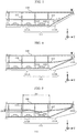
- FIG. 7 is a schematic cross-sectional view of a configuration of liquid crystal module 100 according to example 2.
- FIG. 7 shows a cross section of liquid crystal module 100 which includes a portion extending from flat portion 111A to the upper part of side wall 111B of back frame 111.
- the configuration common to from FIG. 1 to FIG. 4 is indicated by a more simplified diagram in consideration of visibility.
- the wedge shape in FIG. 7 indicates a position of the upper outer edge (upper end) of the active area of display panel 102 in the lateral view.
- the configuration of liquid crystal module 100 is common to a portion extending from flat portion 111A to the lower part, right part, or left part of side wall 111B.
- Embodiment 1 differs from Embodiment 1 or the comparative example shown in FIG. 6 .
- liquid crystal module 100 has a gap between luminance-equalizing sheet 107 and side wall 111B of back frame 111.
- the configuration that allows the light from LEDs 113 to travel while being reflected between luminance-equalizing sheet 107 and reflective sheet 108 also allows the light to reach the peripheral areas.
- liquid crystal module 100 in order to allow light from LEDs 113 to reach the peripheral areas, includes luminance-equalizing sheet 107 smaller in outside dimension than luminance-equalizing sheet 107 of the comparative example shown in FIG. 6 , and has a gap for allowing passage of light between luminance-equalizing sheet 107 and side wall 111B of back frame 111.
- the white arrow in FIG. 7 indicates a path along which the light from LEDs 113 enters the peripheral areas.
- liquid crystal module 100 is capable of displaying an image with greater luminance uniformity from the center to peripheral areas of the screen.
- FIG. 8 is a schematic cross-sectional view of a configuration of liquid crystal module 100 according to example 3.
- FIG. 8 shows a cross section of liquid crystal module 100 which includes a portion extending from flat portion 111A to the upper part of side wall 111B of back frame 111.
- the configuration common to from FIG. 1 to FIG. 4 is indicated by a more simplified diagram in consideration of visibility.
- the wedge shape in FIG. 8 indicates a position of the upper outer edge (upper end) of the active area of display panel 102 in the lateral view.
- the configuration of liquid crystal module 100 is common to a portion extending from flat portion 111A to the lower part, right part, or left part of side wall 111B.
- side wall 111B of back frame 111 includes standing wall 1110 extending from the outer edge of side wall 111B as the starting point toward diffuser panel 106. Further, the outer edge of luminance-equalizing sheet 107 reaches the outer edge of side wall 111B and substantially overlaps the starting point of standing wall 1110. Accordingly, compared to liquid crystal module 100 shown in FIG. 5 , a distance that is substantially equal to the height (the length in the Z axis direction) of standing wall 1110 is maintained between diffuser panel 106 and luminance-equalizing sheet 107.
- luminance-equalizing sheet 107 is extremely close to diffuser panel 106 in the vicinity of the outer edge of the active area of display panel 102.
- luminance-equalizing sheet 107 casts a shadow on diffuser panel 106 in the vicinity of the outer edge of the active area, and a luminance difference between a portion on which this shadow is cast and the other portion can appear on the screen as luminance unevenness visible to the user.
- Standing wall 1110 may be substantially directly below the active area of display panel 102. Further, more preferably, standing wall 1110 may be spaced outward from the active area by approximately 1 mm to 2 mm. Accordingly, entire display panel 102 can be more surely included in an illumination range of light going through luminance-equalizing sheet 107.
- liquid crystal module 100 is capable of displaying an image with greater luminance uniformity from the center to peripheral areas of the screen.
- standing wall 1110 when a distance between back frame 111 and diffuser panel 106 is 20 mm, and a distance between back frame 111 and luminance-equalizing sheet 107 is 10 mm, standing wall 1110 having a height of approximately 3 mm may be provided.
- these sizes are changed in design for adjustment according to the size or desired exterior appearance of entire liquid crystal module 100, the density or emission intensity of arranged LEDs 113, or the like, and are not intended to limit the configuration of liquid crystal module 100 according to Embodiment 3.
- side wall 111B includes standing wall 1110 extending from the outer edge as the starting point toward diffuser panel 106, and the outer edge of luminance-equalizing sheet 107 substantially overlaps the starting point of diffuser panel 106.
- Image display apparatus 10 a gap according to the height of standing wall 1110 is provided between diffuser panel 106 and the outer edge of luminance-equalizing sheet 107 closest to diffuser panel 106. Accordingly, luminance-equalizing sheet 107 is inhibited from casting a shadow on diffuser panel 106 or a cast shadow is thinned.
- Image display apparatus 10 is capable of displaying an image with greater luminance uniformity from the center to peripheral areas of the screen.
- the curved shape of luminance-equalizing sheet 107 in example 1 or 3 may be the shape of molded luminance-equalizing sheet 107 itself.
- luminance-equalizing sheet 107 which originally has a flat shape and is larger in outside dimension than the active area of display panel 102, may be caused to form such a shape by bringing the outer edge of luminance-equalizing sheet 107 into contact with back frame 111 and warping luminance-equalizing sheet 107.
- FIG. 9 is a schematic cross-sectional view of such a distortion caused in liquid crystal module 100 according to example 3. Like FIG. 5 etc., FIG. 9 shows a cross section of liquid crystal module 100 which includes a portion extending from flat portion 111A to the upper part of side wall 111B of back frame 111.
- an undulating distortion of luminance-equalizing sheet 107 is seen in a range indicated by double-headed arrow D1 pointing to the right and the left.
- Double-headed arrow D2 pointing upward and downward indicates the magnitude of the undulating distortion.
- FIG. 10 is a schematic cross-sectional view of a configuration of liquid crystal module 100 according to the present invention.
- FIG. 11 is a front view of the configuration of liquid crystal module 100 according to the present invention.
- FIG. 10 shows a cross section of liquid crystal module 100 which includes a portion extending from flat portion 111A to the upper part of side wall 111B of back frame 111.
- FIG. 11 shows an upper right corner portion of back frame 111 seen from front (a side on which display panel 102 is present).
- FIG. 10 and FIG. 11 shows the configuration common to from FIG. 1 to FIG.
- dashed lines indicate valley fold portions
- alternate long and short dash lines indicate virtual lines passing through equidistant points between horizontally or vertically adjacent two of LEDs 113.
- Liquid crystal module 100 further includes auxiliary support pins 114 that are pillar-shaped and on the virtual lines (the alternate long and short dash lines in FIG. 11 ) on which support pins 112 are disposed.
- Auxiliary support pins 114 also support luminance-equalizing sheet 107 between diffuser panel 106 and back frame 111. Positions in the Z axis direction at which auxiliary support pins 114 support luminance-equalizing sheet 107, that is, the height from back frame 111 is the same as the height at which support pins 112 support luminance-equalizing sheet 107.
- the set of auxiliary support pins 114 is closer to the outer edge of flat portion 111A than support pins 112 and LEDs 113. Further, intervals between the set of auxiliary support pins 114 are narrower than intervals between support pins 112.
- auxiliary support pin 114 is disposed closer to the outer edge of flat portion 111A than LEDs 113 in flat portion 111A is that it is intended to maintain, in a further inner region of luminance-equalizing sheet 107 directly below which LEDs 113 in the rows and columns are present, a wider area which has no distortion and is continuously flat.
- the distortion of luminance-equalizing sheet 107 is minimized in a narrower area (double-headed arrow D3 in FIG. 10 ) outside of the region.
- auxiliary support pins 114 are disposed on the above lines is that it is intended to minimize the impact of a shadow extending toward side wall 111B created by auxiliary support pins 114 blocking light from LEDs 113, by keeping auxiliary support pins 114 at a distance from all LEDs 113 as much as possible.
- liquid crystal module 100 is capable of displaying an image with greater luminance uniformity from the center to peripheral areas of the screen.
- auxiliary support pins 114 make a set above, three or more auxiliary support pins 114 may make a set according to the need for minimizing a distortion.
- auxiliary support pins 114 blocking light from LEDs 113 impacts on luminance uniformity, it is desirable that the number of auxiliary support pins 114 making a set be as few as possible.
- support pin 112 on one end of each row or each column and at least one support pin at shorter intervals from support pin 112 may be interpreted as a set of auxiliary support pins 114.
- auxiliary support pins 114 make a set, intervals between the auxiliary support pins need not be equal.
- auxiliary support pins 114 support luminance-equalizing sheet 107 at a predetermined height from back frame 111 to minimize the distortion of luminance-equalizing sheet 107, and the predetermined height is the same as the height at which support pins 112 support luminance-equalizing sheet 107.
- all auxiliary support pins 114 need not support diffuser panel 106.
- auxiliary support pins 114 other than one auxiliary support pin 114 may have a height and a structure for supporting luminance-equalizing sheet 107, e.g. may include two flanges that clamp luminance-equalizing sheet 107 at a predetermined height and be shorter than support pins 112.
- auxiliary support pins 114 can reduce an amount of light going through luminance-equalizing sheet 107 blocked by auxiliary support pins 114 as much as the configuration with no auxiliary support pin 114 as shown in FIG. 8 . Further, in connection with the configuration, auxiliary support pins 114 need not have the same shape as support pins 112, and may be thinner than support pins 112, for example. Consequently, it is possible to further reduce the impact of the shadow cast on side wall 111B.
- liquid crystal module 100 is capable of displaying an image with greater luminance uniformity from the center to peripheral areas of the screen.
- image display apparatus 10 In image display apparatus 10 according to the above-described present variation, support pins 112 are on the lines passing through the equidistant points between horizontally or vertically adjacent two of LEDs 113 serving as the light sources.
- image display apparatus 10 further includes a set of at least two auxiliary support pins 114 that are pillar-shaped and support luminance-equalizing sheet 107 between back frame 111 and diffuser panel 106 in positions which are on the lines and at which auxiliary support pins 114 are closer to the outer edge of flat portion 111A than support pins 112 and LEDs 113.
- the intervals between the set of at least two auxiliary support pins 114 is narrower than the intervals between support pins 112.
- auxiliary support pins 114 reduce the curvature of the distortion of luminance-equalizing sheet 107 that can be caused by the stress. Since this reduces the variation in distance between LEDs 113 and luminance-equalizing sheet 107, the effect of adjusting the distribution characteristics of light with luminance-equalizing sheet 107 can be produced almost as intended by design. Further, auxiliary support pins 114 are closer to the outer edge of luminance-equalizing sheet 107, and thus a more widely continuous flat area is provided in luminance-equalizing sheet 107. Accordingly, image display apparatus 10 is capable of displaying an image with greater luminance uniformity from the center to peripheral areas of the screen.
- examples 1 to 3 have been given as examples of the techniques disclosed in the present application.
- the techniques disclosed in the present application are not limited to these examples, and are also applicable to embodiments as a result of appropriate modification, replacement, addition, and omission, for instance.
- each of examples 1 to 3 and the variation are also applicable to image display apparatuses using a direct-lit backlight system which includes light sources other than LEDs.
- Examples of the light sources other than the LEDs included in the image display apparatuses to which each of examples 1 to 3 and the variation are applied include a cold-cathode tube and a fluorescent tube.
- reflective sheet 108 clamped by support pins 112 and back frame 111 has been given as an example of the configuration for reflecting light from the light sources and guiding the reflected light to the outer edge of the active area
- the configuration of image display apparatus 10 is not limited to this.
- the entire front surface of back frame 111 may be coated with a material having high optical reflectance or back frame 111 itself may be made of a material having high optical reflectance.
- reflective sheet 108 as a reflective material and back frame 111 may be considered as identical, and, for example, the distance between luminance-equalizing sheet 107 and back frame 111 in the above description can be interpreted as being the same as the distance between luminance-equalizing sheet 107 and reflective sheet 108.
- image display apparatus 10 has been described as, for example, a liquid crystal television, other examples of image display apparatus 10 include a monitor for personal computers and a display for digital signage.
- examples 1 to 3 and the variation described above are intended to illustrate the techniques in the present application, and thus various modifications, replacements, addition, omissions, etc. may be made within the scope of claims and the equivalents thereof.
- the present disclosure is applicable to image display apparatuses that look thin in appearance by reducing the thickness of a peripheral portion more than the thickness of other portions. More specifically, the present disclosure is applicable to television receivers, monitors, displays for digital signage, etc.
Landscapes
- Physics & Mathematics (AREA)
- Nonlinear Science (AREA)
- General Physics & Mathematics (AREA)
- Optics & Photonics (AREA)
- Mathematical Physics (AREA)
- Chemical & Material Sciences (AREA)
- Crystallography & Structural Chemistry (AREA)
- Engineering & Computer Science (AREA)
- Theoretical Computer Science (AREA)
- General Engineering & Computer Science (AREA)
- Planar Illumination Modules (AREA)
- Devices For Indicating Variable Information By Combining Individual Elements (AREA)
- Liquid Crystal (AREA)
Claims (8)
- Appareil d'affichage d'image, comprenant :un panneau d'affichage (102) ;un cadre arrière (111) qui comporte une partie plate (111A) ayant une surface sensiblement plate plus petite qu'une zone active du panneau d'affichage, et une paroi latérale (111B) qui s'élève à partir d'un bord externe de la partie plate (111A) et atteint un bord externe de la zone active dans une vue de face ;une pluralité de sources de lumière (113) qui sont agencées en rangées et en colonnes à des intervalles sensiblement égaux dans la partie plate (111A) ;une pluralité de broches de support (112) qui sont en forme de pilier et agencées en rangées et en colonnes à des intervalles sensiblement égaux dans des positions dans la partie plate (111A) et à distance de la pluralité de sources de lumière (113) ;un panneau diffuseur (106) qui est en forme de plaque, est supporté par des pointes de la pluralité de broches de support (112) et du cadre arrière (111), et émet de manière diffuse la lumière provenant de la pluralité de sources de lumière (113) vers le panneau d'affichage (102) ; etune feuille d'égalisation de luminance (107) qui est en forme de feuille, est supportée à des positions intermédiaires sur la pluralité de broches de support (112), entre le panneau diffuseur (102) et le cadre arrière (111), a un bord externe qui chevauche sensiblement le bord externe de la zone active, et transmet une partie de la lumière provenant de la pluralité de sources de lumière (113) vers le panneau diffuseur (102),dans lequel la feuille d'égalisation de luminance (107) fait saillie d'une manière incurvée vers la paroi latérale (111B) entre le panneau diffuseur (102) et la paroi latérale (111B) de sorte que la distance entre la feuille d'égalisation de luminance (107) et le cadre arrière (111) diminue progressivement du bord externe de la partie plate (111A) à un bord externe de la paroi latérale (111B),dans lequel la pluralité de broches de support (112) se situent sur des lignes dont chacune passe par des points équidistants entre deux sources de lumière horizontalement ou verticalement adjacentes de la pluralité de sources de lumière (113),l'appareil d'affichage d'image comprend en outre un ensemble d'au moins deux broches de support auxiliaires (114) qui sont en forme de pilier et supportent la feuille d'égalisation de luminance (107) entre le cadre arrière (111) et le panneau diffuseur (106) dans des positions qui sont adjacentes les unes aux autres et situées sur la même ligne parmi les lignes et auxquelles l'ensemble d'au moins deux broches de support auxiliaires (114) sont plus proches du bord externe de la partie plate (111A) que la pluralité de broches de support (112) et la pluralité de sources de lumière (113).
- Appareil d'affichage d'image selon la revendication 1,
dans lequel une paroi verticale (1110) s'étend depuis le bord externe de la paroi latérale (111B) en tant que point de départ vers le panneau diffuseur (106), et
le bord externe de la feuille d'égalisation de luminance (107) chevauche sensiblement le point de départ. - Appareil d'affichage d'image selon la revendication 2, dans lequel la paroi verticale (1110) est directement en dessous de la zone active du panneau d'affichage.
- Appareil d'affichage d'image selon la revendication 2 ou 3, dans lequel la paroi verticale (1110) est espacée vers l'extérieur de la zone active de 1 mm à 2 mm.
- Appareil d'affichage d'image selon l'une quelconque des revendications 1 à 4,
dans lequel des intervalles entre deux broches de support auxiliaires (114) dans l'ensemble d'au moins deux broches de support auxiliaires (114) sont plus étroits que des intervalles entre la pluralité de broches de support (112). - Appareil d'affichage d'image selon la revendication 5, dans lequel les broches de support auxiliaires (114) supportent la feuille d'égalisation de luminance (107) à une hauteur prédéterminée à partir du cadre arrière (111), et la hauteur prédéterminée est la même que la hauteur à laquelle les broches de support (112) supportent la feuille d'égalisation de luminance (107).
- Appareil d'affichage d'image selon la revendication 5, dans lequel parmi un ensemble d'au moins deux broches de support auxiliaires (114), des broches de support auxiliaires (114) autres qu'une première broche de support auxiliaire (114) ont une hauteur plus courte que les broches de support (112), et la première broche de support auxiliaire (114) supporte la feuille d'égalisation de luminance (107) à une hauteur prédéterminée à partir du cadre arrière (111), et la hauteur prédéterminée est la même que la hauteur à laquelle les broches de support (112) supportent la feuille d'égalisation de luminance (107).
- Appareil d'affichage d'image selon la revendication 7, dans lequel les broches de support auxiliaires (114) sont plus minces que les broches de support (112).
Applications Claiming Priority (3)
| Application Number | Priority Date | Filing Date | Title |
|---|---|---|---|
| US201762456836P | 2017-02-09 | 2017-02-09 | |
| JP2017161516 | 2017-08-24 | ||
| PCT/JP2018/003999 WO2018147268A1 (fr) | 2017-02-09 | 2018-02-06 | Dispositif d'affichage d'image |
Publications (3)
| Publication Number | Publication Date |
|---|---|
| EP3581995A1 EP3581995A1 (fr) | 2019-12-18 |
| EP3581995A4 EP3581995A4 (fr) | 2019-12-18 |
| EP3581995B1 true EP3581995B1 (fr) | 2021-03-31 |
Family
ID=66095839
Family Applications (1)
| Application Number | Title | Priority Date | Filing Date |
|---|---|---|---|
| EP18750651.4A Active EP3581995B1 (fr) | 2017-02-09 | 2018-02-06 | Dispositif d'affichage d'image |
Country Status (3)
| Country | Link |
|---|---|
| US (1) | US10761372B2 (fr) |
| EP (1) | EP3581995B1 (fr) |
| JP (1) | JP7108897B2 (fr) |
Families Citing this family (5)
| Publication number | Priority date | Publication date | Assignee | Title |
|---|---|---|---|---|
| KR102493155B1 (ko) | 2018-03-26 | 2023-01-27 | 엘지전자 주식회사 | 디스플레이 디바이스 |
| JP7275428B2 (ja) * | 2019-03-08 | 2023-05-18 | 船井電機・ホールディングス株式会社 | バックライト装置及び液晶表示装置 |
| JP7468165B2 (ja) * | 2020-06-05 | 2024-04-16 | 船井電機株式会社 | 発光装置および表示装置 |
| US11287696B2 (en) * | 2020-07-09 | 2022-03-29 | Sharp Kabushiki Kaisha | Liquid crystal display module |
| CN114355674B (zh) * | 2022-01-13 | 2023-06-02 | 武汉华星光电技术有限公司 | 背光模组和液晶显示装置 |
Family Cites Families (17)
| Publication number | Priority date | Publication date | Assignee | Title |
|---|---|---|---|---|
| TWI283321B (en) * | 2004-06-18 | 2007-07-01 | Au Optronics Corp | Supporter and LED light-source module using the same |
| TWI255896B (en) | 2005-01-19 | 2006-06-01 | Au Optronics Corp | Backlight module |
| JP4788231B2 (ja) | 2005-04-28 | 2011-10-05 | ソニー株式会社 | 支柱及び液晶表示装置 |
| US20060285356A1 (en) * | 2005-06-21 | 2006-12-21 | K-Bridge Electronics Co., Ltd. | Side-edge backlight module dimming pack |
| JP5050498B2 (ja) * | 2006-11-21 | 2012-10-17 | ソニー株式会社 | 光源装置、バックライト装置、液晶表示装置及びバックライト装置の製造方法 |
| JP2008209551A (ja) | 2007-02-26 | 2008-09-11 | Funai Electric Co Ltd | 液晶モジュール |
| TWI361308B (en) * | 2007-06-21 | 2012-04-01 | Chimei Innolux Corp | Backlight module and liquid crystal display device |
| US8177382B2 (en) | 2008-03-11 | 2012-05-15 | Cree, Inc. | Apparatus and methods for multiplanar optical diffusers and display panels for using the same |
| JP2010033818A (ja) | 2008-07-28 | 2010-02-12 | Sonac Kk | 均一発光構造を有する面状発光装置 |
| JP4539782B2 (ja) * | 2008-07-31 | 2010-09-08 | エプソンイメージングデバイス株式会社 | 電子機器 |
| EP2450619A4 (fr) * | 2009-07-02 | 2013-10-30 | Sharp Kk | Dispositif d'éclairage, appareil d'affichage et équipement de réception de télévision |
| JP5648162B2 (ja) | 2009-11-16 | 2015-01-07 | 株式会社オプトデザイン | 面光源ユニット、面照明装置及び液晶表示装置 |
| JP2012243653A (ja) | 2011-05-20 | 2012-12-10 | Sharp Corp | バックライト装置および表示装置 |
| JP2015038828A (ja) * | 2013-08-19 | 2015-02-26 | 船井電機株式会社 | 表示装置 |
| JP2015040919A (ja) | 2013-08-20 | 2015-03-02 | 船井電機株式会社 | 表示装置 |
| WO2017002307A1 (fr) | 2015-07-01 | 2017-01-05 | パナソニックIpマネジメント株式会社 | Dispositif de rétroéclairage et dispositif d'affichage à cristaux liquides |
| JP6644510B2 (ja) | 2015-10-02 | 2020-02-12 | シャープ株式会社 | 照明装置、表示装置及びテレビ受信装置 |
-
2018
- 2018-02-06 EP EP18750651.4A patent/EP3581995B1/fr active Active
- 2018-02-06 JP JP2018535190A patent/JP7108897B2/ja not_active Expired - Fee Related
- 2018-02-06 US US16/094,299 patent/US10761372B2/en not_active Expired - Fee Related
Non-Patent Citations (1)
| Title |
|---|
| None * |
Also Published As
| Publication number | Publication date |
|---|---|
| JP7108897B2 (ja) | 2022-07-29 |
| EP3581995A1 (fr) | 2019-12-18 |
| EP3581995A4 (fr) | 2019-12-18 |
| JPWO2018147268A1 (ja) | 2019-12-12 |
| US10761372B2 (en) | 2020-09-01 |
| US20190113808A1 (en) | 2019-04-18 |
Similar Documents
| Publication | Publication Date | Title |
|---|---|---|
| EP3581995B1 (fr) | Dispositif d'affichage d'image | |
| EP3318792B1 (fr) | Dispositif de rétroéclairage et dispositif d'affichage à cristaux liquides | |
| EP3318793B1 (fr) | Dispositif de rétroéclairage et dispositif d'affichage à cristaux liquides | |
| EP3121645B1 (fr) | Dispositif d'affichage à cristaux liquides | |
| US20120050645A1 (en) | Image display apparatus | |
| JP2013161793A (ja) | バックライトユニット用の支持部材と、それを備えたバックライトユニットおよび映像表示装置 | |
| EP3581998B1 (fr) | Dispositif d'affichage d'image | |
| US8690409B2 (en) | Backlight assembly and display apparatus having the same | |
| US9575238B2 (en) | Back light module | |
| US8228458B2 (en) | Backlight unit and liquid crystal display | |
| US10620476B2 (en) | Image display apparatus | |
| CN100365488C (zh) | 直下型背光灯 | |
| WO2013038802A1 (fr) | Dispositif d'émission de lumière par la surface et dispositif d'affichage à cristaux liquides doté de celui-ci | |
| US11175016B2 (en) | Planar illumination device with spacer between lens and diffuser | |
| US10914985B2 (en) | Image display apparatus and support pin | |
| US20160209579A1 (en) | Display apparatus | |
| US10401679B2 (en) | Display apparatus | |
| JP4499692B2 (ja) | バックライトユニット及びこれを備えた液晶表示装置 | |
| US10914984B2 (en) | Image display apparatus and support pin | |
| US8757829B2 (en) | Backlight source and display device | |
| US20110115838A1 (en) | Liquid crystal display device and liquid crystal display unit | |
| US10317732B2 (en) | Display apparatus with backlight unit | |
| KR100701083B1 (ko) | 액정표시장치용 백라이트 유니트 | |
| WO2018147268A1 (fr) | Dispositif d'affichage d'image | |
| KR102166052B1 (ko) | 백라이트 유닛 및 이를 포함하는 액정표시장치 |
Legal Events
| Date | Code | Title | Description |
|---|---|---|---|
| STAA | Information on the status of an ep patent application or granted ep patent |
Free format text: STATUS: THE INTERNATIONAL PUBLICATION HAS BEEN MADE |
|
| PUAI | Public reference made under article 153(3) epc to a published international application that has entered the european phase |
Free format text: ORIGINAL CODE: 0009012 |
|
| STAA | Information on the status of an ep patent application or granted ep patent |
Free format text: STATUS: REQUEST FOR EXAMINATION WAS MADE |
|
| 17P | Request for examination filed |
Effective date: 20190723 |
|
| A4 | Supplementary search report drawn up and despatched |
Effective date: 20191004 |
|
| AK | Designated contracting states |
Kind code of ref document: A1 Designated state(s): AL AT BE BG CH CY CZ DE DK EE ES FI FR GB GR HR HU IE IS IT LI LT LU LV MC MK MT NL NO PL PT RO RS SE SI SK SM TR |
|
| AX | Request for extension of the european patent |
Extension state: BA ME |
|
| STAA | Information on the status of an ep patent application or granted ep patent |
Free format text: STATUS: EXAMINATION IS IN PROGRESS |
|
| DAV | Request for validation of the european patent (deleted) | ||
| DAX | Request for extension of the european patent (deleted) | ||
| 17Q | First examination report despatched |
Effective date: 20200423 |
|
| GRAP | Despatch of communication of intention to grant a patent |
Free format text: ORIGINAL CODE: EPIDOSNIGR1 |
|
| STAA | Information on the status of an ep patent application or granted ep patent |
Free format text: STATUS: GRANT OF PATENT IS INTENDED |
|
| INTG | Intention to grant announced |
Effective date: 20201215 |
|
| GRAS | Grant fee paid |
Free format text: ORIGINAL CODE: EPIDOSNIGR3 |
|
| GRAA | (expected) grant |
Free format text: ORIGINAL CODE: 0009210 |
|
| STAA | Information on the status of an ep patent application or granted ep patent |
Free format text: STATUS: THE PATENT HAS BEEN GRANTED |
|
| AK | Designated contracting states |
Kind code of ref document: B1 Designated state(s): AL AT BE BG CH CY CZ DE DK EE ES FI FR GB GR HR HU IE IS IT LI LT LU LV MC MK MT NL NO PL PT RO RS SE SI SK SM TR |
|
| REG | Reference to a national code |
Ref country code: GB Ref legal event code: FG4D Ref country code: CH Ref legal event code: EP |
|
| REG | Reference to a national code |
Ref country code: AT Ref legal event code: REF Ref document number: 1377614 Country of ref document: AT Kind code of ref document: T Effective date: 20210415 |
|
| REG | Reference to a national code |
Ref country code: DE Ref legal event code: R096 Ref document number: 602018014858 Country of ref document: DE |
|
| REG | Reference to a national code |
Ref country code: IE Ref legal event code: FG4D |
|
| REG | Reference to a national code |
Ref country code: LT Ref legal event code: MG9D |
|
| PG25 | Lapsed in a contracting state [announced via postgrant information from national office to epo] |
Ref country code: BG Free format text: LAPSE BECAUSE OF FAILURE TO SUBMIT A TRANSLATION OF THE DESCRIPTION OR TO PAY THE FEE WITHIN THE PRESCRIBED TIME-LIMIT Effective date: 20210630 Ref country code: FI Free format text: LAPSE BECAUSE OF FAILURE TO SUBMIT A TRANSLATION OF THE DESCRIPTION OR TO PAY THE FEE WITHIN THE PRESCRIBED TIME-LIMIT Effective date: 20210331 Ref country code: HR Free format text: LAPSE BECAUSE OF FAILURE TO SUBMIT A TRANSLATION OF THE DESCRIPTION OR TO PAY THE FEE WITHIN THE PRESCRIBED TIME-LIMIT Effective date: 20210331 Ref country code: NO Free format text: LAPSE BECAUSE OF FAILURE TO SUBMIT A TRANSLATION OF THE DESCRIPTION OR TO PAY THE FEE WITHIN THE PRESCRIBED TIME-LIMIT Effective date: 20210630 |
|
| PG25 | Lapsed in a contracting state [announced via postgrant information from national office to epo] |
Ref country code: SE Free format text: LAPSE BECAUSE OF FAILURE TO SUBMIT A TRANSLATION OF THE DESCRIPTION OR TO PAY THE FEE WITHIN THE PRESCRIBED TIME-LIMIT Effective date: 20210331 Ref country code: RS Free format text: LAPSE BECAUSE OF FAILURE TO SUBMIT A TRANSLATION OF THE DESCRIPTION OR TO PAY THE FEE WITHIN THE PRESCRIBED TIME-LIMIT Effective date: 20210331 Ref country code: LV Free format text: LAPSE BECAUSE OF FAILURE TO SUBMIT A TRANSLATION OF THE DESCRIPTION OR TO PAY THE FEE WITHIN THE PRESCRIBED TIME-LIMIT Effective date: 20210331 |
|
| REG | Reference to a national code |
Ref country code: NL Ref legal event code: MP Effective date: 20210331 |
|
| REG | Reference to a national code |
Ref country code: AT Ref legal event code: MK05 Ref document number: 1377614 Country of ref document: AT Kind code of ref document: T Effective date: 20210331 |
|
| PG25 | Lapsed in a contracting state [announced via postgrant information from national office to epo] |
Ref country code: SM Free format text: LAPSE BECAUSE OF FAILURE TO SUBMIT A TRANSLATION OF THE DESCRIPTION OR TO PAY THE FEE WITHIN THE PRESCRIBED TIME-LIMIT Effective date: 20210331 Ref country code: NL Free format text: LAPSE BECAUSE OF FAILURE TO SUBMIT A TRANSLATION OF THE DESCRIPTION OR TO PAY THE FEE WITHIN THE PRESCRIBED TIME-LIMIT Effective date: 20210331 Ref country code: AT Free format text: LAPSE BECAUSE OF FAILURE TO SUBMIT A TRANSLATION OF THE DESCRIPTION OR TO PAY THE FEE WITHIN THE PRESCRIBED TIME-LIMIT Effective date: 20210331 Ref country code: CZ Free format text: LAPSE BECAUSE OF FAILURE TO SUBMIT A TRANSLATION OF THE DESCRIPTION OR TO PAY THE FEE WITHIN THE PRESCRIBED TIME-LIMIT Effective date: 20210331 Ref country code: EE Free format text: LAPSE BECAUSE OF FAILURE TO SUBMIT A TRANSLATION OF THE DESCRIPTION OR TO PAY THE FEE WITHIN THE PRESCRIBED TIME-LIMIT Effective date: 20210331 Ref country code: LT Free format text: LAPSE BECAUSE OF FAILURE TO SUBMIT A TRANSLATION OF THE DESCRIPTION OR TO PAY THE FEE WITHIN THE PRESCRIBED TIME-LIMIT Effective date: 20210331 |
|
| PG25 | Lapsed in a contracting state [announced via postgrant information from national office to epo] |
Ref country code: IS Free format text: LAPSE BECAUSE OF FAILURE TO SUBMIT A TRANSLATION OF THE DESCRIPTION OR TO PAY THE FEE WITHIN THE PRESCRIBED TIME-LIMIT Effective date: 20210731 Ref country code: SK Free format text: LAPSE BECAUSE OF FAILURE TO SUBMIT A TRANSLATION OF THE DESCRIPTION OR TO PAY THE FEE WITHIN THE PRESCRIBED TIME-LIMIT Effective date: 20210331 Ref country code: PT Free format text: LAPSE BECAUSE OF FAILURE TO SUBMIT A TRANSLATION OF THE DESCRIPTION OR TO PAY THE FEE WITHIN THE PRESCRIBED TIME-LIMIT Effective date: 20210802 Ref country code: RO Free format text: LAPSE BECAUSE OF FAILURE TO SUBMIT A TRANSLATION OF THE DESCRIPTION OR TO PAY THE FEE WITHIN THE PRESCRIBED TIME-LIMIT Effective date: 20210331 Ref country code: PL Free format text: LAPSE BECAUSE OF FAILURE TO SUBMIT A TRANSLATION OF THE DESCRIPTION OR TO PAY THE FEE WITHIN THE PRESCRIBED TIME-LIMIT Effective date: 20210331 |
|
| REG | Reference to a national code |
Ref country code: DE Ref legal event code: R097 Ref document number: 602018014858 Country of ref document: DE |
|
| PG25 | Lapsed in a contracting state [announced via postgrant information from national office to epo] |
Ref country code: AL Free format text: LAPSE BECAUSE OF FAILURE TO SUBMIT A TRANSLATION OF THE DESCRIPTION OR TO PAY THE FEE WITHIN THE PRESCRIBED TIME-LIMIT Effective date: 20210331 Ref country code: DK Free format text: LAPSE BECAUSE OF FAILURE TO SUBMIT A TRANSLATION OF THE DESCRIPTION OR TO PAY THE FEE WITHIN THE PRESCRIBED TIME-LIMIT Effective date: 20210331 Ref country code: ES Free format text: LAPSE BECAUSE OF FAILURE TO SUBMIT A TRANSLATION OF THE DESCRIPTION OR TO PAY THE FEE WITHIN THE PRESCRIBED TIME-LIMIT Effective date: 20210331 |
|
| PLBE | No opposition filed within time limit |
Free format text: ORIGINAL CODE: 0009261 |
|
| STAA | Information on the status of an ep patent application or granted ep patent |
Free format text: STATUS: NO OPPOSITION FILED WITHIN TIME LIMIT |
|
| 26N | No opposition filed |
Effective date: 20220104 |
|
| PG25 | Lapsed in a contracting state [announced via postgrant information from national office to epo] |
Ref country code: IS Free format text: LAPSE BECAUSE OF FAILURE TO SUBMIT A TRANSLATION OF THE DESCRIPTION OR TO PAY THE FEE WITHIN THE PRESCRIBED TIME-LIMIT Effective date: 20210731 |
|
| PG25 | Lapsed in a contracting state [announced via postgrant information from national office to epo] |
Ref country code: IT Free format text: LAPSE BECAUSE OF FAILURE TO SUBMIT A TRANSLATION OF THE DESCRIPTION OR TO PAY THE FEE WITHIN THE PRESCRIBED TIME-LIMIT Effective date: 20210331 |
|
| PG25 | Lapsed in a contracting state [announced via postgrant information from national office to epo] |
Ref country code: MC Free format text: LAPSE BECAUSE OF FAILURE TO SUBMIT A TRANSLATION OF THE DESCRIPTION OR TO PAY THE FEE WITHIN THE PRESCRIBED TIME-LIMIT Effective date: 20210331 |
|
| REG | Reference to a national code |
Ref country code: CH Ref legal event code: PL |
|
| REG | Reference to a national code |
Ref country code: BE Ref legal event code: MM Effective date: 20220228 |
|
| PG25 | Lapsed in a contracting state [announced via postgrant information from national office to epo] |
Ref country code: LU Free format text: LAPSE BECAUSE OF NON-PAYMENT OF DUE FEES Effective date: 20220206 |
|
| PG25 | Lapsed in a contracting state [announced via postgrant information from national office to epo] |
Ref country code: LI Free format text: LAPSE BECAUSE OF NON-PAYMENT OF DUE FEES Effective date: 20220228 Ref country code: IE Free format text: LAPSE BECAUSE OF NON-PAYMENT OF DUE FEES Effective date: 20220206 Ref country code: CH Free format text: LAPSE BECAUSE OF NON-PAYMENT OF DUE FEES Effective date: 20220228 |
|
| PG25 | Lapsed in a contracting state [announced via postgrant information from national office to epo] |
Ref country code: BE Free format text: LAPSE BECAUSE OF NON-PAYMENT OF DUE FEES Effective date: 20220228 |
|
| PGFP | Annual fee paid to national office [announced via postgrant information from national office to epo] |
Ref country code: FR Payment date: 20230424 Year of fee payment: 7 |
|
| PG25 | Lapsed in a contracting state [announced via postgrant information from national office to epo] |
Ref country code: MK Free format text: LAPSE BECAUSE OF FAILURE TO SUBMIT A TRANSLATION OF THE DESCRIPTION OR TO PAY THE FEE WITHIN THE PRESCRIBED TIME-LIMIT Effective date: 20210331 Ref country code: CY Free format text: LAPSE BECAUSE OF FAILURE TO SUBMIT A TRANSLATION OF THE DESCRIPTION OR TO PAY THE FEE WITHIN THE PRESCRIBED TIME-LIMIT Effective date: 20210331 |
|
| PGFP | Annual fee paid to national office [announced via postgrant information from national office to epo] |
Ref country code: DE Payment date: 20230420 Year of fee payment: 7 Ref country code: GB Payment date: 20240219 Year of fee payment: 7 |
|
| PG25 | Lapsed in a contracting state [announced via postgrant information from national office to epo] |
Ref country code: HU Free format text: LAPSE BECAUSE OF FAILURE TO SUBMIT A TRANSLATION OF THE DESCRIPTION OR TO PAY THE FEE WITHIN THE PRESCRIBED TIME-LIMIT; INVALID AB INITIO Effective date: 20180206 |
|
| PG25 | Lapsed in a contracting state [announced via postgrant information from national office to epo] |
Ref country code: MT Free format text: LAPSE BECAUSE OF FAILURE TO SUBMIT A TRANSLATION OF THE DESCRIPTION OR TO PAY THE FEE WITHIN THE PRESCRIBED TIME-LIMIT Effective date: 20210331 |
|
| PG25 | Lapsed in a contracting state [announced via postgrant information from national office to epo] |
Ref country code: GR Free format text: LAPSE BECAUSE OF NON-PAYMENT OF DUE FEES Effective date: 20210331 |
|
| PG25 | Lapsed in a contracting state [announced via postgrant information from national office to epo] |
Ref country code: GR Free format text: LAPSE BECAUSE OF NON-PAYMENT OF DUE FEES Effective date: 20210331 |
|
| REG | Reference to a national code |
Ref country code: DE Ref legal event code: R119 Ref document number: 602018014858 Country of ref document: DE |
|
| GBPC | Gb: european patent ceased through non-payment of renewal fee |
Effective date: 20250206 |
|
| PG25 | Lapsed in a contracting state [announced via postgrant information from national office to epo] |
Ref country code: TR Free format text: LAPSE BECAUSE OF FAILURE TO SUBMIT A TRANSLATION OF THE DESCRIPTION OR TO PAY THE FEE WITHIN THE PRESCRIBED TIME-LIMIT Effective date: 20210331 |
|
| PG25 | Lapsed in a contracting state [announced via postgrant information from national office to epo] |
Ref country code: DE Free format text: LAPSE BECAUSE OF NON-PAYMENT OF DUE FEES Effective date: 20250902 |
|
| PG25 | Lapsed in a contracting state [announced via postgrant information from national office to epo] |
Ref country code: GB Free format text: LAPSE BECAUSE OF NON-PAYMENT OF DUE FEES Effective date: 20250206 |
|
| PG25 | Lapsed in a contracting state [announced via postgrant information from national office to epo] |
Ref country code: FR Free format text: LAPSE BECAUSE OF NON-PAYMENT OF DUE FEES Effective date: 20250228 |