EP3581996B1 - Dispositif d'affichage d'image - Google Patents
Dispositif d'affichage d'image Download PDFInfo
- Publication number
- EP3581996B1 EP3581996B1 EP18750875.9A EP18750875A EP3581996B1 EP 3581996 B1 EP3581996 B1 EP 3581996B1 EP 18750875 A EP18750875 A EP 18750875A EP 3581996 B1 EP3581996 B1 EP 3581996B1
- Authority
- EP
- European Patent Office
- Prior art keywords
- metal member
- substrate
- metal
- display panel
- disposed
- Prior art date
- Legal status (The legal status is an assumption and is not a legal conclusion. Google has not performed a legal analysis and makes no representation as to the accuracy of the status listed.)
- Active
Links
Images


Classifications
-
- H—ELECTRICITY
- H01—ELECTRIC ELEMENTS
- H01R—ELECTRICALLY-CONDUCTIVE CONNECTIONS; STRUCTURAL ASSOCIATIONS OF A PLURALITY OF MUTUALLY-INSULATED ELECTRICAL CONNECTING ELEMENTS; COUPLING DEVICES; CURRENT COLLECTORS
- H01R12/00—Structural associations of a plurality of mutually-insulated electrical connecting elements, specially adapted for printed circuits, e.g. printed circuit boards [PCB], flat or ribbon cables, or like generally planar structures, e.g. terminal strips, terminal blocks; Coupling devices specially adapted for printed circuits, flat or ribbon cables, or like generally planar structures; Terminals specially adapted for contact with, or insertion into, printed circuits, flat or ribbon cables, or like generally planar structures
- H01R12/70—Coupling devices
- H01R12/71—Coupling devices for rigid printing circuits or like structures
- H01R12/72—Coupling devices for rigid printing circuits or like structures coupling with the edge of the rigid printed circuits or like structures
- H01R12/722—Coupling devices for rigid printing circuits or like structures coupling with the edge of the rigid printed circuits or like structures coupling devices mounted on the edge of the printed circuits
- H01R12/728—Coupling devices without an insulating housing provided on the edge of the PCB
-
- F—MECHANICAL ENGINEERING; LIGHTING; HEATING; WEAPONS; BLASTING
- F21—LIGHTING
- F21S—NON-PORTABLE LIGHTING DEVICES; SYSTEMS THEREOF; VEHICLE LIGHTING DEVICES SPECIALLY ADAPTED FOR VEHICLE EXTERIORS
- F21S2/00—Systems of lighting devices, not provided for in main groups F21S4/00 - F21S10/00 or F21S19/00, e.g. of modular construction
-
- G—PHYSICS
- G02—OPTICS
- G02F—OPTICAL DEVICES OR ARRANGEMENTS FOR THE CONTROL OF LIGHT BY MODIFICATION OF THE OPTICAL PROPERTIES OF THE MEDIA OF THE ELEMENTS INVOLVED THEREIN; NON-LINEAR OPTICS; FREQUENCY-CHANGING OF LIGHT; OPTICAL LOGIC ELEMENTS; OPTICAL ANALOGUE/DIGITAL CONVERTERS
- G02F1/00—Devices or arrangements for the control of the intensity, colour, phase, polarisation or direction of light arriving from an independent light source, e.g. switching, gating or modulating; Non-linear optics
- G02F1/01—Devices or arrangements for the control of the intensity, colour, phase, polarisation or direction of light arriving from an independent light source, e.g. switching, gating or modulating; Non-linear optics for the control of the intensity, phase, polarisation or colour
- G02F1/13—Devices or arrangements for the control of the intensity, colour, phase, polarisation or direction of light arriving from an independent light source, e.g. switching, gating or modulating; Non-linear optics for the control of the intensity, phase, polarisation or colour based on liquid crystals, e.g. single liquid crystal display cells
- G02F1/133—Constructional arrangements; Operation of liquid crystal cells; Circuit arrangements
- G02F1/1333—Constructional arrangements; Manufacturing methods
- G02F1/133308—Support structures for LCD panels, e.g. frames or bezels
-
- G—PHYSICS
- G02—OPTICS
- G02F—OPTICAL DEVICES OR ARRANGEMENTS FOR THE CONTROL OF LIGHT BY MODIFICATION OF THE OPTICAL PROPERTIES OF THE MEDIA OF THE ELEMENTS INVOLVED THEREIN; NON-LINEAR OPTICS; FREQUENCY-CHANGING OF LIGHT; OPTICAL LOGIC ELEMENTS; OPTICAL ANALOGUE/DIGITAL CONVERTERS
- G02F1/00—Devices or arrangements for the control of the intensity, colour, phase, polarisation or direction of light arriving from an independent light source, e.g. switching, gating or modulating; Non-linear optics
- G02F1/01—Devices or arrangements for the control of the intensity, colour, phase, polarisation or direction of light arriving from an independent light source, e.g. switching, gating or modulating; Non-linear optics for the control of the intensity, phase, polarisation or colour
- G02F1/13—Devices or arrangements for the control of the intensity, colour, phase, polarisation or direction of light arriving from an independent light source, e.g. switching, gating or modulating; Non-linear optics for the control of the intensity, phase, polarisation or colour based on liquid crystals, e.g. single liquid crystal display cells
- G02F1/133—Constructional arrangements; Operation of liquid crystal cells; Circuit arrangements
- G02F1/1333—Constructional arrangements; Manufacturing methods
- G02F1/1335—Structural association of cells with optical devices, e.g. polarisers or reflectors
- G02F1/1336—Illuminating devices
- G02F1/133602—Direct backlight
- G02F1/133603—Direct backlight with LEDs
-
- G—PHYSICS
- G02—OPTICS
- G02F—OPTICAL DEVICES OR ARRANGEMENTS FOR THE CONTROL OF LIGHT BY MODIFICATION OF THE OPTICAL PROPERTIES OF THE MEDIA OF THE ELEMENTS INVOLVED THEREIN; NON-LINEAR OPTICS; FREQUENCY-CHANGING OF LIGHT; OPTICAL LOGIC ELEMENTS; OPTICAL ANALOGUE/DIGITAL CONVERTERS
- G02F1/00—Devices or arrangements for the control of the intensity, colour, phase, polarisation or direction of light arriving from an independent light source, e.g. switching, gating or modulating; Non-linear optics
- G02F1/01—Devices or arrangements for the control of the intensity, colour, phase, polarisation or direction of light arriving from an independent light source, e.g. switching, gating or modulating; Non-linear optics for the control of the intensity, phase, polarisation or colour
- G02F1/13—Devices or arrangements for the control of the intensity, colour, phase, polarisation or direction of light arriving from an independent light source, e.g. switching, gating or modulating; Non-linear optics for the control of the intensity, phase, polarisation or colour based on liquid crystals, e.g. single liquid crystal display cells
- G02F1/133—Constructional arrangements; Operation of liquid crystal cells; Circuit arrangements
- G02F1/1333—Constructional arrangements; Manufacturing methods
- G02F1/1335—Structural association of cells with optical devices, e.g. polarisers or reflectors
- G02F1/1336—Illuminating devices
- G02F1/133602—Direct backlight
- G02F1/133605—Direct backlight including specially adapted reflectors
-
- G—PHYSICS
- G02—OPTICS
- G02F—OPTICAL DEVICES OR ARRANGEMENTS FOR THE CONTROL OF LIGHT BY MODIFICATION OF THE OPTICAL PROPERTIES OF THE MEDIA OF THE ELEMENTS INVOLVED THEREIN; NON-LINEAR OPTICS; FREQUENCY-CHANGING OF LIGHT; OPTICAL LOGIC ELEMENTS; OPTICAL ANALOGUE/DIGITAL CONVERTERS
- G02F1/00—Devices or arrangements for the control of the intensity, colour, phase, polarisation or direction of light arriving from an independent light source, e.g. switching, gating or modulating; Non-linear optics
- G02F1/01—Devices or arrangements for the control of the intensity, colour, phase, polarisation or direction of light arriving from an independent light source, e.g. switching, gating or modulating; Non-linear optics for the control of the intensity, phase, polarisation or colour
- G02F1/13—Devices or arrangements for the control of the intensity, colour, phase, polarisation or direction of light arriving from an independent light source, e.g. switching, gating or modulating; Non-linear optics for the control of the intensity, phase, polarisation or colour based on liquid crystals, e.g. single liquid crystal display cells
- G02F1/133—Constructional arrangements; Operation of liquid crystal cells; Circuit arrangements
- G02F1/1333—Constructional arrangements; Manufacturing methods
- G02F1/1335—Structural association of cells with optical devices, e.g. polarisers or reflectors
- G02F1/1336—Illuminating devices
- G02F1/133602—Direct backlight
- G02F1/133608—Direct backlight including particular frames or supporting means
-
- H—ELECTRICITY
- H01—ELECTRIC ELEMENTS
- H01R—ELECTRICALLY-CONDUCTIVE CONNECTIONS; STRUCTURAL ASSOCIATIONS OF A PLURALITY OF MUTUALLY-INSULATED ELECTRICAL CONNECTING ELEMENTS; COUPLING DEVICES; CURRENT COLLECTORS
- H01R13/00—Details of coupling devices of the kinds covered by groups H01R12/70 or H01R24/00 - H01R33/00
- H01R13/02—Contact members
- H01R13/04—Pins or blades for co-operation with sockets
-
- H—ELECTRICITY
- H01—ELECTRIC ELEMENTS
- H01R—ELECTRICALLY-CONDUCTIVE CONNECTIONS; STRUCTURAL ASSOCIATIONS OF A PLURALITY OF MUTUALLY-INSULATED ELECTRICAL CONNECTING ELEMENTS; COUPLING DEVICES; CURRENT COLLECTORS
- H01R13/00—Details of coupling devices of the kinds covered by groups H01R12/70 or H01R24/00 - H01R33/00
- H01R13/02—Contact members
- H01R13/20—Pins, blades, or sockets shaped, or provided with separate member, to retain co-operating parts together
-
- H—ELECTRICITY
- H01—ELECTRIC ELEMENTS
- H01R—ELECTRICALLY-CONDUCTIVE CONNECTIONS; STRUCTURAL ASSOCIATIONS OF A PLURALITY OF MUTUALLY-INSULATED ELECTRICAL CONNECTING ELEMENTS; COUPLING DEVICES; CURRENT COLLECTORS
- H01R13/00—Details of coupling devices of the kinds covered by groups H01R12/70 or H01R24/00 - H01R33/00
- H01R13/64—Means for preventing incorrect coupling
- H01R13/641—Means for preventing incorrect coupling by indicating incorrect coupling; by indicating correct or full engagement
-
- G—PHYSICS
- G02—OPTICS
- G02F—OPTICAL DEVICES OR ARRANGEMENTS FOR THE CONTROL OF LIGHT BY MODIFICATION OF THE OPTICAL PROPERTIES OF THE MEDIA OF THE ELEMENTS INVOLVED THEREIN; NON-LINEAR OPTICS; FREQUENCY-CHANGING OF LIGHT; OPTICAL LOGIC ELEMENTS; OPTICAL ANALOGUE/DIGITAL CONVERTERS
- G02F1/00—Devices or arrangements for the control of the intensity, colour, phase, polarisation or direction of light arriving from an independent light source, e.g. switching, gating or modulating; Non-linear optics
- G02F1/01—Devices or arrangements for the control of the intensity, colour, phase, polarisation or direction of light arriving from an independent light source, e.g. switching, gating or modulating; Non-linear optics for the control of the intensity, phase, polarisation or colour
- G02F1/13—Devices or arrangements for the control of the intensity, colour, phase, polarisation or direction of light arriving from an independent light source, e.g. switching, gating or modulating; Non-linear optics for the control of the intensity, phase, polarisation or colour based on liquid crystals, e.g. single liquid crystal display cells
- G02F1/133—Constructional arrangements; Operation of liquid crystal cells; Circuit arrangements
- G02F1/1333—Constructional arrangements; Manufacturing methods
- G02F1/1335—Structural association of cells with optical devices, e.g. polarisers or reflectors
- G02F1/1336—Illuminating devices
- G02F1/133602—Direct backlight
- G02F1/133612—Electrical details
-
- G—PHYSICS
- G02—OPTICS
- G02F—OPTICAL DEVICES OR ARRANGEMENTS FOR THE CONTROL OF LIGHT BY MODIFICATION OF THE OPTICAL PROPERTIES OF THE MEDIA OF THE ELEMENTS INVOLVED THEREIN; NON-LINEAR OPTICS; FREQUENCY-CHANGING OF LIGHT; OPTICAL LOGIC ELEMENTS; OPTICAL ANALOGUE/DIGITAL CONVERTERS
- G02F1/00—Devices or arrangements for the control of the intensity, colour, phase, polarisation or direction of light arriving from an independent light source, e.g. switching, gating or modulating; Non-linear optics
- G02F1/01—Devices or arrangements for the control of the intensity, colour, phase, polarisation or direction of light arriving from an independent light source, e.g. switching, gating or modulating; Non-linear optics for the control of the intensity, phase, polarisation or colour
- G02F1/13—Devices or arrangements for the control of the intensity, colour, phase, polarisation or direction of light arriving from an independent light source, e.g. switching, gating or modulating; Non-linear optics for the control of the intensity, phase, polarisation or colour based on liquid crystals, e.g. single liquid crystal display cells
- G02F1/133—Constructional arrangements; Operation of liquid crystal cells; Circuit arrangements
- G02F1/136—Liquid crystal cells structurally associated with a semi-conducting layer or substrate, e.g. cells forming part of an integrated circuit
- G02F1/1362—Active matrix addressed cells
- G02F1/136204—Arrangements to prevent high voltage or static electricity failures
-
- G—PHYSICS
- G02—OPTICS
- G02F—OPTICAL DEVICES OR ARRANGEMENTS FOR THE CONTROL OF LIGHT BY MODIFICATION OF THE OPTICAL PROPERTIES OF THE MEDIA OF THE ELEMENTS INVOLVED THEREIN; NON-LINEAR OPTICS; FREQUENCY-CHANGING OF LIGHT; OPTICAL LOGIC ELEMENTS; OPTICAL ANALOGUE/DIGITAL CONVERTERS
- G02F2202/00—Materials and properties
- G02F2202/22—Antistatic materials or arrangements
-
- G—PHYSICS
- G02—OPTICS
- G02F—OPTICAL DEVICES OR ARRANGEMENTS FOR THE CONTROL OF LIGHT BY MODIFICATION OF THE OPTICAL PROPERTIES OF THE MEDIA OF THE ELEMENTS INVOLVED THEREIN; NON-LINEAR OPTICS; FREQUENCY-CHANGING OF LIGHT; OPTICAL LOGIC ELEMENTS; OPTICAL ANALOGUE/DIGITAL CONVERTERS
- G02F2202/00—Materials and properties
- G02F2202/28—Adhesive materials or arrangements
-
- H—ELECTRICITY
- H01—ELECTRIC ELEMENTS
- H01R—ELECTRICALLY-CONDUCTIVE CONNECTIONS; STRUCTURAL ASSOCIATIONS OF A PLURALITY OF MUTUALLY-INSULATED ELECTRICAL CONNECTING ELEMENTS; COUPLING DEVICES; CURRENT COLLECTORS
- H01R13/00—Details of coupling devices of the kinds covered by groups H01R12/70 or H01R24/00 - H01R33/00
- H01R13/02—Contact members
- H01R13/10—Sockets for co-operation with pins or blades
- H01R13/11—Resilient sockets
- H01R13/114—Resilient sockets co-operating with pins or blades having a square transverse section
Definitions
- the present disclosure relates to an image display apparatus that displays an image and a connecting pin.
- Patent Literature (PTL) 1 discloses an image display apparatus including: a display panel; a lower frame disposed on the back surface side of the display panel, a direct backlight supported by the lower frame; and a reflective sheet that is disposed between the display panel and the backlight and reflects light from the backlight toward the back surface of the display panel.
- the backlight includes a plurality of substrates and light emitting diodes (LEDs) mounted on the plurality of substrates.
- a connector electrically connected with LEDs is mounted on each of the plurality of substrates.
- the connector includes a metal terminal and a resin housing covering the metal terminal.
- the connector on one substrate is electrically connected with the connector on another substrate via a lead wire having connectors.
- US 2014/211452 A1 relates to a direct type backlight module and a display device.
- GB 1 398 934 A relates to a detecting coupling.
- JP 2013 229229 A relates to an illuminating device, a display apparatus and a television receiver.
- US2015023001 A discloses the features of the preamble of claim 1.
- PTL 1 Japanese Unexamined Patent Application Publication No. 2016-62765 .
- the present disclosure provides an image display apparatus and a connecting pin that can reduce generation of unevenness in the luminance of an image displayed on a display panel.
- An image display apparatus can reduce generation of unevenness in the luminance of an image displayed on a display panel.
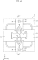
- FIG. 1 is a perspective view illustrating image display apparatus 2 according to the embodiment.
- FIG. 2 is an exploded perspective view of liquid crystal module 4 of image display apparatus 2 according to the embodiment.
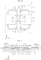
- FIG. 3 illustrates a portion of liquid crystal module 4 according to the embodiment. Note that FIG. 3 illustrates, among the components of liquid crystal module 4, lower frame 10 and backlight 12 only.
- image display apparatus 2 is a liquid crystal television receiver of the flat panel display type, for example.
- Image display apparatus 2 includes liquid crystal module 4, back cover 6 that covers the back surface of liquid crystal module 4, and stand 8 that supports liquid crystal module 4.
- Liquid crystal module 4 is a unit for displaying an image (including a still image and a moving image). As illustrated in FIG. 2 , liquid crystal module 4 includes lower frame 10 (an example of a support member), backlight 12, reflective sheet 14 (an example of a reflector), a plurality of support pins 16, uniform luminance plate 18, diffuser plate 20, optical sheet unit 22, mold frame 24, display panel 26, and bezel 28.
- lower frame 10 an example of a support member
- backlight 12 an example of a reflector
- reflective sheet 14 an example of a reflector
- a plurality of support pins 16 uniform luminance plate 18, diffuser plate 20, optical sheet unit 22, mold frame 24, display panel 26, and bezel 28.
- Lower frame 10 supports backlight 12 and optical sheet unit 22, for example, and is also called a base plate.
- Lower frame 10 is formed using a thin sheet metal and is formed into a rectangular shape in an XY plan view.
- a plurality of recessed portions 30 are formed in the front surface of lower frame 10 (a surface closer to display panel 26), corresponding to connecting portions of LED substrates 36 (described later) and relay substrates 40 (described later).
- Each of the plurality of recessed portions 30 is formed by drawing a sheet metal, for example, and is formed to be depressed toward back cover 6 (the Z axis negative side).
- the plurality of recessed portions 30 are located at intervals along the longitudinal direction of lower frame 10 (the X axis direction) at the central region of lower frame 10 in a direction (the Y axis direction) transverse to the longitudinal direction of lower frame 10. Further, as illustrated in FIG. 5 described later, each of the plurality of recessed portions 30 has a plurality of through-holes 31 each overlapping with first metal member 48 (described later) and second metal member 50 (described later) fit with each other in the XY plan view. Note that first metal member 48 and second metal member 50 constitute connecting pin 51 for connecting two different members with each other. (see FIG. 4A described later).
- Backlight 12 is a direct backlight for emitting light toward the back surface of display panel 26. As illustrated in FIG. 2 and FIG. 3 , backlight 12 includes a plurality of LED sheets 32 and a plurality of relay sheets 34.
- each of the plurality of LED sheets 32 is for emitting light and is supported by the front surface of lower frame 10.
- the plurality of LED sheets 32 are disposed at intervals along the longitudinal direction of lower frame 10, in a region above the central region of lower frame 10 in the transverse direction (the Y axis positive side) and a region below the central region (the Y axis negative side).
- Each of the plurality of LED sheets 32 includes elongated LED substrate 36 (an example of a first substrate) and a plurality of LEDs 38 (an example of a light source) mounted on a mounting surface of LED substrate 36.
- LED substrate 36 is a sheet-shaped flexible printed board having flexibility, and is formed using polyimide, for example.
- the thickness (size in the Z axis direction) of LED substrate 36 is about 0.1 mm, for example.
- a reflective layer for reflecting light from the plurality of LEDs 38 is formed on the mounting surface of LED substrate 36.
- LED substrate 36 is attached to the front surface of lower frame 10 using a double-sided adhesive tape, for example, and is disposed extending along the transverse direction of lower frame 10.
- the plurality of LEDs 38 are each a chip LED, for example, and are disposed at intervals along the longitudinal direction (the Y axis direction) of LED substrate 36.
- each of the plurality of relay sheets 34 is for electrically relaying the plurality of LED sheets 32 and is supported by the front surface of lower frame 10.
- the plurality of relay sheets 34 are disposed at intervals along the longitudinal direction of lower frame 10, in the central region of lower frame 10 in the transverse direction.
- Each of the plurality of relay sheets 34 includes elongated relay substrate 40 (an example of a second substrate) and circuit unit 42 mounted on a mounting surface of relay substrate 40.
- Relay substrate 40 is a sheet-shaped flexible printed board having flexibility, and is formed using polyimide, for example.
- the thickness (size in the Z axis direction) of relay substrate 40 is about 0.1 mm, for example.
- a reflective layer for reflecting light from the plurality of LEDs 38 is formed on the mounting surface of relay substrate 40.
- a plurality of slits 44 are formed in relay substrate 40 to enhance the flexibility. The plurality of slits 44 are located at intervals along the longitudinal direction of relay substrate 40 (the X axis direction).
- Relay substrate 40 is attached to the front surface of lower frame 10 using a double-sided adhesive tape, for example, and is disposed extending along the longitudinal direction of lower frame 10.
- Circuit unit 42 is, for example, an electric circuit for supplying electric power, a control signal, etc. to each of the plurality of LEDs 38 of LED sheets 32.
- LED substrate 36 and relay substrate 40 are electrically connected.
- the present embodiment is characterized in a connecting structure that electrically connects LED substrate 36 and relay substrate 40.
- the connecting structure for LED substrate 36 and relay substrate 40 will be described later.
- Reflective sheet 14 reflects light from the plurality of LEDs 38 toward the back surface of display panel 26.
- Reflective sheet 14 has flexibility and is formed using, for example, an electrically insulative white resin such as polyethylene terephthalate (PET).
- PET polyethylene terephthalate
- Reflective sheet 14 is disposed to cover the plurality of LED sheets 32 and the plurality of relay sheets 34, and is attached to the front surface of lower frame 10 using a double-sided adhesive tape, for example. That is to say, reflective sheet 14 is disposed between display panel 26 and both of the plurality of LED sheets 32 and the plurality of relay sheets 34 so as to cover later-described first metal members 48 and second metal members 50.
- reflective sheet 14 has a plurality of holes 46 corresponding to the plurality of LEDs 38. As illustrated in FIG. 5 described later, the plurality of LEDs 38 are inserted through the plurality of holes 46 of reflective sheet 14 to be exposed on the reflective surface of reflective sheet 14 (a surface closer to display panel 26).
- Each of the plurality of support pins 16 supports diffuser plate 20. Each support pin 16 is disposed on the reflective surface of reflective sheet 14. Reflective sheet 14 is sandwiched between support pins 16 and lower frame 10. Each support pin 16 includes a flange and a pin protruding from the flange.
- Uniform luminance plate 18 makes the luminance of light from the plurality of LEDs 38 uniform, and is what is known as Flatter (registered trademark). Uniform luminance plate 18 is opposed to reflective sheet 14. Uniform luminance plate 18 has a plurality of support holes corresponding to the plurality of support pins 16. With the pins of support pins 16 being inserted through the plurality of support holes, uniform luminance plate 18 is supported by the flanges of support pins 16. Uniform luminance plate 18 also has a plurality of illumination holes different in size. Specifically, in uniform luminance plate 18, illumination holes having an extremely small diameter are formed directly above LEDs 38. The diameter of the illumination holes increases with an increase in distance from LEDs 38. By passing through the plurality of illumination holes of uniform luminance plate 18, the light from the plurality of LEDs 38 can have smoother distribution properties.
- Diffuser plate 20 diffuses light from the plurality of LEDs 38. When supported by the pins of the plurality of support pins 16, diffuser plate 20 is opposed to uniform luminance plate 18. Further, a perimeter portion of diffuser plate 20 is supported by lower frame 10. Since diffuser plate 20 further diffuses the light whose distribution properties are made smoother by uniform luminance plate 18, diffuser plate 20 emits light whose luminance is less uneven.
- Optical sheet unit 22 includes a plurality of optical sheets having different optical properties.
- the plurality of optical sheets are disposed, in a state of being overlapped with each other, between display panel 26 and diffuser plate 20.
- the plurality of optical sheets include, for example, a) a vertical prism sheet for collecting light emitted from diffuser plate 20, b) a horizontal prism sheet for collecting light emitted from diffuser plate 20, c) a reflective polarizing sheet for polarizing light emitted from diffuser plate 20 (for example, Dual Brightness Enhancement Film (DBEF) (registered trademark) sheet of Sumitomo 3M Limited), etc.
- DBEF Dual Brightness Enhancement Film
- Mold frame 24 is formed into a rectangular frame shape in an XY plan view. Mold frame 24 supports display panel 26. The components from optical sheet unit 22 to backlight 12 are sandwiched between mold frame 24 and lower frame 10.
- Display panel 26 displays an image.
- Display panel 26 is what is known as a liquid crystal cell, in which a liquid crystal is sealed between a plurality of glass plates.
- the front surface of display panel 26 is a display surface for displaying an image.
- a perimeter portion of display panel 26 is supported by mold frame 24 via a cushion.
- Bezel 28 protects the perimeter portion of display panel 26.
- Bezel 28 is formed into a rectangular frame shape in an XY plan view, and disposed so as to cover the perimeter portion of display panel 26. The components from display panel 26 to lower frame 10 are sandwiched between bezel 28 and back cover 6 (see FIG. 1 ).
- bezel 28 is formed using, for example, a resin such as polycarbonate.
- back cover 6 is disposed so as to cover the back surface of lower frame 10 of liquid crystal module 4.
- Back cover 6 is formed using, for example, a resin such as polycarbonate.
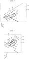
- FIG. 4A is an enlarged view of a portion of liquid crystal module 4 of image display apparatus 2 according to the embodiment, surrounded by dashedline frame P shown in FIG. 3 .
- FIG. 4B illustrates liquid crystal module 4 in FIG. 4A , before LED substrate 36 and relay substrate 40 are connected with each other.
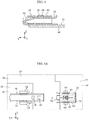
- FIG. 5 is a cross-sectional view of liquid crystal module 4 of image display apparatus 2 according to the embodiment, taken along line V-V in FIG. 4A .
- FIG. 6 is an enlarged perspective view of first metal member 48 according to the embodiment.
- FIG. 7 is an enlarged perspective view of second metal member 50 according to the embodiment.
- FIG. 8 is a cross-sectional view of second metal member 50 according to the embodiment, taken along line VIII-VIII in FIG. 7 .
- FIG. 9A illustrates first metal member 48 and second metal member 50 before being fitted with each other.
- FIG. 9B illustrates first metal member 48 and second metal member 50 when fitted with each other.
- FIG. 10 is a cross-sectional view of first metal member 48 and second metal member 50 taken along line X-X in FIG. 9B .
- a pair of first metal members 48 are disposed at an end portion of LED substrate 36 in the longitudinal direction thereof.
- Paired first metal members 48 are both mounted on the mounting surface of LED substrate 36 in a state of being exposed, and are disposed with a space therebetween along a direction (the X axis direction) of LED substrate 36 transverse to the longitudinal direction of LED substrate 36.
- Paired first metal members 48 are both electrically connected to each of the plurality of LEDs 38 mounted on LED substrate 36.
- the respective tip portions of paired first metal members 48 protrude from an end portion of LED substrate 36 in the longitudinal direction thereof.
- One of paired first metal members 48 functions as a positive electrode terminal, for example, and the other functions as a negative electrode terminal, for example.
- height H1 of first metal members 48 from the mounting surface of LED substrate 36 is about 1.5 mm, for example.
- a plurality of pairs of second metal members 50 are disposed at both end portions of relay substrate 40 in the transverse direction thereof (end portions in the Y axis direction).
- the plurality of pairs of second metal members 50 are disposed at intervals along the longitudinal direction of relay substrates 40.
- Paired second metal members 50 are both mounted on the mounting surface of relay substrate 40 in a state of being exposed, and are disposed with a space therebetween along the longitudinal direction of relay substrate 40.
- Paired second metal members 50 are both electrically connected to circuit unit 42 mounted on relay substrate 40.
- the respective tip portions of paired second metal members 50 protrude from an end portion of relay substrate 40 in the transverse direction thereof.
- One of paired second metal members 50 functions as a positive electrode terminal, for example, and the other functions as a negative electrode terminal, for example.
- height H2 of second metal members 50 from the mounting surface of relay substrate 40 is about 1.7 mm, for example.
- Paired first metal members 48 are removably fit with a corresponding pair of second metal members 50.
- the connecting portion of LED substrate 36 and relay substrate 40 is bent along recessed portion 30 of lower frame 10. That is to say, a pair of first metal members 48 and a pair of second metal members 50 fit with each other are disposed in recessed portion 30 of lower frame 10. Further, the pair of first metal members 48 and the pair of second metal members 50 fit with each other are covered with reflective sheet 14. Note that, for convenience of illustration, first metal members 48 and second metal members 50 are illustrated in a simplified manner in FIG. 3 to FIG. 5 .
- first metal members 48 and second metal members 50 will be described in detail.
- first metal members 48 are, for example, female metal pins formed using an electrically-conductive metal such as phosphor bronze.
- First metal members 48 each include body portion 52 having an elongated half tubular shape and a plurality of leg portions 54 formed at both end portions of body portion 52 in the transverse direction thereof (end portions in the X axis direction).
- One end portion of body portion 52 in the longitudinal direction thereof protrudes from one end portion of LED substrate 36 in the longitudinal direction thereof.
- the top surface of body portion 52 (the surface opposed to LED substrate 36) has fitting hole 56 and index hole 58 (an example of an index portion).
- Fitting hole 56 and index hole 58 are located at positions off-centered toward one end portion of body portion 52 in the longitudinal direction thereof. Index hole 58 is located closer to LED substrate 36 than fitting hole 56 is. Each of the plurality of leg portions 54 is fixed to the mounting surface of LED substrate 36 by, for example, soldering.
- second metal members 50 are male metal pins formed using an electrically-conductive metal such as phosphor bronze.
- Second metal members 50 each include body portion 60 having an elongated tubular shape, fitting piece 62 disposed inside body portion 60, and a plurality of leg portions 64 formed at both end portions of body portion 60 in the transverse direction thereof (end portions in the X axis direction).
- One end portion of body portion 60 in the longitudinal direction thereof protrudes from one end portion of relay substrate 40 in the transverse direction thereof.
- the top surface of body portion 60 (the surface opposed to relay substrate 40) has standby hole 66. Standby hole 66 is located at the central portion of body portion 60 in the longitudinal direction thereof.
- fitting piece 62 is elongated while bending along the longitudinal direction of body portion 60.
- One end portion of fitting piece 62 in the longitudinal direction thereof is connected to the bottom surface of body portion 60 (the surface closer to relay substrate 40).
- Operation portion 70 protruding outside body portion 60 is formed at the other end portion of fitting piece 62 in the longitudinal direction thereof.
- Fitting protrusion 68 is formed at the central portion of fitting piece 62 in the longitudinal direction thereof by, for example, cutting and raising processing. Fitting piece 62 is biased toward the top surface of body portion 60.
- fitting protrusion 68 is in standby hole 66 of body portion 60.
- Each of the plurality of leg portions 64 is fixed to the mounting surface of relay substrate 40 by, for example, soldering.
- one end portion of body portion 52 of first metal member 48 in the longitudinal direction thereof is inserted into body portion 60 of second metal member 50 from one end portion of body portion 60 in the longitudinal direction thereof.
- the end portion of body portion 52 in the longitudinal direction thereof is inserted between the top surface of body portion 60 and fitting piece 62 while pressing down fitting piece 62 in a direction (the Z axis negative direction) in which fitting piece 62 separates from the top surface of body portion 60. Accordingly, fitting protrusion 68 is pulled out from standby hole 66.
- fitting protrusion 68 is fitted into fitting hole 56 by the biasing force of fitting piece 62. Accordingly, first metal member 48 and second metal member 50 are fitted with each other, thereby electrically connecting LED substrate 36 and relay substrate 40.
- index hole 58 of body portion 52 is covered with the top surface of body portion 60 and thus becomes invisible from outside.
- index hole 58 of body portion 52 is present outside the top surface of body portion 60, and is thus visible from outside. Accordingly, by visually checking whether or not index hole 58 of body portion 52 is visible, a user can easily determine whether or not first metal member 48 and second metal member 50 are fitted with each other.
- FIG. 11 is an enlarged cross-sectional view of a portion of liquid crystal module 102 of image display apparatus 100 according to the comparative example.
- a plurality of LED substrates 104 are supported by lower frame 106.
- Each of the plurality of LED substrates 104 is formed using a rigid substrate.
- LED 108 and connector 110 are mounted on the mounting surface of each LED substrate 104.
- Connector 110 includes metal terminal 112 and resin housing 114 covering metal terminal 112.
- Connector 110 on one LED substrate 104 is electrically connected with connector 110 on another LED substrate 104 via lead wire 116 having connectors.
- connector 110 includes housing 114, height H3 of connector 110 from LED substrate 104 is as high as 3 mm to 5 mm, for example. For this reason, when reflective sheet 118 is attached to lower frame 106, bulge portion 120 largely bulging locally due to connectors 110 is formed in reflective sheet 118. As a consequence, bulge portion 120 of reflective sheet 118 blocks a portion of light from LEDs 108, resulting in a problem of generation of unevenness in the luminance of an image displayed on the display panel (not illustrated).
- image display apparatus includes: display panel 26 that displays an image on a front surface; LED substrate 36 which is disposed on a back surface side of display panel 26 and on which LED 38 is mounted; relay substrate 40 which is disposed on the back surface side of display panel 26 and on which circuit unit 42 is mounted; first metal member 48 disposed on LED substrate 36 and electrically connected with LED 38; second metal member 50 disposed on relay substrate 40, electrically connected with circuit unit 42, and fitted with first metal member 48; and reflective sheet 14 that is electrically insulative and disposed between display panel 26 and both of LED substrate 36 and relay substrate 40 so as to cover at least first metal member 48 and second metal member 50, reflective sheet 14 reflecting light from LED 38 toward a back surface of display panel 26.
- One of first metal member 48 and second metal member 50 includes index hole 58. When first metal member 48 and second metal member 50 are fitted with each other, index hole 58 is covered by the other of first metal member 48 and second metal member 50.
- first metal member 48 and second metal member 50 are covered with reflective sheet 14 that is electrically insulative, it is possible to ensure electrical insulation between each of first metal member 48 and second metal member 50 and other electrically conductive members.
- first metal member 48 and second metal member 50 fitted with each other it is possible to simplify the layout of the wire between LED substrate 36 and relay substrate 40.
- index hole 58 the user can easily determine whether or not first metal member 48 and second metal member 50 are fitted with each other.
- each of LED substrate 36 and relay substrate 40 has flexibility.
- each of LED substrate 36 and relay substrate 40 it is possible to relieve stress generated between first metal member 48 and second metal member 50, thereby making it possible to reduce the occurrence of an electrical connection failure between first metal member 48 and second metal member 50.
- image display apparatus 2 further includes lower frame 10 that is disposed on the back surface side of display panel 26 and supports LED substrate 36 and relay substrate 40.
- Lower frame 10 includes recessed portion 30 in which first metal member 48 and second metal member 50 are disposed.
- recessed portion 30 of lower frame 10 can absorb height H1 of first metal member 48 from the mounting surface of LED substrate 36 and height H2 of second metal member 50 from the mounting surface of relay substrate 40. As a result, it is possible to keep even smaller the size of bulge portion 72 formed in reflective sheet 14 due to first metal member 48 and second metal member 50.
- lower frame 10 further includes through-hole 31 in recessed portion 30. Through-hole 31 overlaps with first metal member 48 and second metal member 50 in a plan view.
- connecting pin 51 includes first metal member 48 and second metal member 50 fitted with first metal member 48.
- One of first metal member 48 and second metal member 50 includes index portion 58.
- index portion 58 is covered by the other of first metal member 48 and second metal member 50.
- index hole 58 is visible, the user can easily determine whether or not first metal member 48 and second metal member 50 are fitted with each other.
- recessed portions 30 are formed in lower frame 10 in the above embodiment, the present disclosure is not limited to this, and recessed portions 30 may be omitted from lower frame 10. Even in this case, it is possible to keep small the size of bulge portion 72 formed in reflective sheet 14 due to first metal member 48 and second metal member 50, thereby making it possible to reduce generation of unevenness in the luminance of an image displayed on display panel 26.
- index hole 58 is formed in body portion 52 of first metal member 48 as an index portion in the above embodiment, the present disclosure is not limited to this.
- a mark such as print or a sticky label
- a protrusion such as a protrusion
- a recess such as a recess
- a notch may be formed in body portion 52 of first metal member 48 as an index portion.
- circuit unit 42 in the above embodiment includes an electric circuit for supplying electric power, a control signal, etc. to each of the plurality of LEDs 38, the present disclosure is not limited to this, and circuit unit 42 may include any circuit.
- first metal members 48 are female metal pins and second metal members 50 are male metal pins in the above embodiment, they can be reversed. That is, first metal members 48 may be male metal pins and second metal members 50 may be female metal pins.
- the structural elements illustrated in the accompanying drawings and described in the detailed description may include not only structural elements essential to solving the problem but also structural elements not essential to solving the problem, in order to provide examples of the above-described techniques. As such, these non-essential structural elements should not be deemed essential due to the mere fact that they are included in the accompanying drawings and the detailed description.
- the present disclosure is applicable to an image display apparatus that displays an image. Specifically, the present disclosure is applicable to an image display apparatus such as a liquid crystal television receiver.
Landscapes
- Physics & Mathematics (AREA)
- Nonlinear Science (AREA)
- Mathematical Physics (AREA)
- Chemical & Material Sciences (AREA)
- Crystallography & Structural Chemistry (AREA)
- General Physics & Mathematics (AREA)
- Optics & Photonics (AREA)
- Engineering & Computer Science (AREA)
- General Engineering & Computer Science (AREA)
- Planar Illumination Modules (AREA)
- Liquid Crystal (AREA)
Claims (4)
- Appareil d'affichage d'image comprenant :un panneau d'affichage (26) qui affiche une image sur une surface avant,un premier substrat (36) qui est disposé sur une surface arrière du panneau d'affichage (26) et sur lequel est montée une source de lumière (38),un second substrat (40) qui est disposé sur la surface arrière du panneau d'affichage (26) et sur lequel est montée une unité de circuit (42),un premier élément métallique (48) disposé sur le premier substrat (36) et relié électriquement à la source de lumière (38),un second élément métallique (50) disposé sur le second substrat (40) relié électriquement à l'unité de circuit (42), etun réflecteur (14) électriquement isolant et disposé entre le panneau d'affichage (26) et à la fois le premier substrat (36) et le second substrat (40) de sorte à recouvrir au moins le premier élément métallique (48) et le second élément métallique (50), le réflecteur (14) étant configuré pour réfléchir la lumière en provenance de la source de lumière (38) vers la surface arrière du panneau d'affichage (26) ,caractérisé en ce quel'un du premier élément métallique (48) et du second élément métallique (50) inclut un organe d'indexage (58), etle second élément métallique (50) est ajusté avec le premier élément métallique (48) pour former une structure de connexion électrique entre le premier substrat (36) et le second substrat (40),lorsque le premier élément métallique (48) et le second élément métallique (50) sont ajustés l'un à l'autre, l'organe d'indexage (58) est recouvert par l'autre du premier élément métallique (48) et du second élément métallique (50) de sorte à ce qu'un utilisateur, grâce à un contrôle visuel de ce que l'organe d'indexage (58) est visible ou non, peut déterminer si le premier élément métallique (48) et le second élément métallique (50) sont ajustés l'un à l'autre.
- Appareil d'affichage d'image selon la revendication 1, dans lequel :
chacun du premier substrat (36) et du second substrat (40) présente une certaine souplesse. - Appareil d'affichage d'image selon la revendication 2, comprenant en outre :
un élément de support (10) qui est disposé sur la surface arrière du panneau d'affichage (26) et supporte le premier substrat (36) et le second substrat (40), dans lequel :
l'élément de support (10) inclut une partie en creux (30) dans laquelle sont disposés le premier élément métallique (48) et le second élément métallique (50). - Appareil d'affichage d'image selon la revendication 3, dans lequel :
l'élément de support (10) inclut en outre un trou traversant (31) dans la partie en creux (30), le trou traversant (31) chevauchant le premier élément métallique (48) et le second élément métallique (50) selon une vue en plan.
Applications Claiming Priority (3)
| Application Number | Priority Date | Filing Date | Title |
|---|---|---|---|
| US201762456912P | 2017-02-09 | 2017-02-09 | |
| JP2017161513 | 2017-08-24 | ||
| PCT/JP2018/004004 WO2018147273A1 (fr) | 2017-02-09 | 2018-02-06 | Dispositif d'affichage d'image et broche de connexion |
Publications (3)
| Publication Number | Publication Date |
|---|---|
| EP3581996A1 EP3581996A1 (fr) | 2019-12-18 |
| EP3581996A4 EP3581996A4 (fr) | 2020-01-15 |
| EP3581996B1 true EP3581996B1 (fr) | 2021-04-14 |
Family
ID=66432105
Family Applications (1)
| Application Number | Title | Priority Date | Filing Date |
|---|---|---|---|
| EP18750875.9A Active EP3581996B1 (fr) | 2017-02-09 | 2018-02-06 | Dispositif d'affichage d'image |
Country Status (2)
| Country | Link |
|---|---|
| US (1) | US10495926B2 (fr) |
| EP (1) | EP3581996B1 (fr) |
Families Citing this family (1)
| Publication number | Priority date | Publication date | Assignee | Title |
|---|---|---|---|---|
| EP4300145A4 (fr) * | 2021-08-17 | 2024-11-27 | Samsung Electronics Co., Ltd. | Appareil d'affichage et unité de rétroéclairage |
Citations (1)
| Publication number | Priority date | Publication date | Assignee | Title |
|---|---|---|---|---|
| US20150023001A1 (en) * | 2013-07-19 | 2015-01-22 | Samsung Display Co., Ltd. | Backlight assembly and a display apparatus having the same |
Family Cites Families (6)
| Publication number | Priority date | Publication date | Assignee | Title |
|---|---|---|---|---|
| GB2398934A (en) * | 2003-02-25 | 2004-09-01 | Guy James Rollo Symons | Detecting coupling |
| JP2008204716A (ja) | 2007-02-19 | 2008-09-04 | Denso Corp | 端子接続構造 |
| JP4968014B2 (ja) | 2007-11-22 | 2012-07-04 | ソニー株式会社 | バックライト装置及び液晶表示装置 |
| JP2013229229A (ja) * | 2012-04-26 | 2013-11-07 | Sharp Corp | 照明装置、表示装置、及びテレビ受信装置 |
| CN103090273B (zh) * | 2013-01-28 | 2015-01-07 | 京东方科技集团股份有限公司 | 一种直下式背光模组及显示装置 |
| JP6297457B2 (ja) | 2014-09-18 | 2018-03-20 | シャープ株式会社 | 照明装置、表示装置、及びテレビ受信装置 |
-
2018
- 2018-02-06 US US16/096,226 patent/US10495926B2/en not_active Expired - Fee Related
- 2018-02-06 EP EP18750875.9A patent/EP3581996B1/fr active Active
Patent Citations (1)
| Publication number | Priority date | Publication date | Assignee | Title |
|---|---|---|---|---|
| US20150023001A1 (en) * | 2013-07-19 | 2015-01-22 | Samsung Display Co., Ltd. | Backlight assembly and a display apparatus having the same |
Also Published As
| Publication number | Publication date |
|---|---|
| EP3581996A4 (fr) | 2020-01-15 |
| US20190146275A1 (en) | 2019-05-16 |
| EP3581996A1 (fr) | 2019-12-18 |
| US10495926B2 (en) | 2019-12-03 |
Similar Documents
| Publication | Publication Date | Title |
|---|---|---|
| US7909480B2 (en) | Light source module, method of fabricating the same, and display device having the light source module | |
| US8157430B2 (en) | Backlight device and planar display device using the same | |
| CN101183195B (zh) | 背光组件和具有该背光组件的液晶显示装置 | |
| US11054570B2 (en) | Liquid crystal display device having a joint portion of a wiring substrate extending from an inside to an outside of the case | |
| US7976183B2 (en) | Backlight unit | |
| JP2011095452A (ja) | 液晶表示モジュール | |
| CN113196674B (zh) | 电子设备 | |
| CN102007522A (zh) | 电子封装件、显示装置以及电子设备 | |
| US8743311B2 (en) | Liquid crystal display | |
| US9111472B2 (en) | Light-emitting diode module, backlight assembly having the LED module and display device having the backlight assembly | |
| KR101979244B1 (ko) | 탑샤시 어셈블리 및 이를 갖는 표시장치 | |
| EP3581996B1 (fr) | Dispositif d'affichage d'image | |
| US8419234B2 (en) | Illumination device, display device, and television receiver apparatus | |
| US10725232B2 (en) | Backlight device and liquid crystal display device comprising the same | |
| WO2011045990A1 (fr) | Dispositif d'affichage | |
| US10302848B2 (en) | Curved display device | |
| US20100117102A1 (en) | Light emitting diodes and backlight unit having the same | |
| EP3582209B1 (fr) | Dispositif d'affichage d'images | |
| CN107923579A (zh) | 照明装置及显示装置 | |
| JP7065355B2 (ja) | 画像表示装置 | |
| CN110967855A (zh) | 显示设备 | |
| KR101401256B1 (ko) | 발광다이오드 모듈과 이를 포함하는 백라이트 유닛 및 디스플레이 장치 | |
| KR20120056935A (ko) | 인쇄 회로 기판 | |
| JP7038635B2 (ja) | 照明装置、表示装置、および、テレビ受信装置 | |
| KR101269387B1 (ko) | 백라이트 유닛 |
Legal Events
| Date | Code | Title | Description |
|---|---|---|---|
| STAA | Information on the status of an ep patent application or granted ep patent |
Free format text: STATUS: THE INTERNATIONAL PUBLICATION HAS BEEN MADE |
|
| PUAI | Public reference made under article 153(3) epc to a published international application that has entered the european phase |
Free format text: ORIGINAL CODE: 0009012 |
|
| STAA | Information on the status of an ep patent application or granted ep patent |
Free format text: STATUS: REQUEST FOR EXAMINATION WAS MADE |
|
| 17P | Request for examination filed |
Effective date: 20190723 |
|
| AK | Designated contracting states |
Kind code of ref document: A1 Designated state(s): AL AT BE BG CH CY CZ DE DK EE ES FI FR GB GR HR HU IE IS IT LI LT LU LV MC MK MT NL NO PL PT RO RS SE SI SK SM TR |
|
| AX | Request for extension of the european patent |
Extension state: BA ME |
|
| A4 | Supplementary search report drawn up and despatched |
Effective date: 20191212 |
|
| RIC1 | Information provided on ipc code assigned before grant |
Ipc: G02F 1/13357 20060101AFI20191206BHEP Ipc: F21S 2/00 20160101ALI20191206BHEP Ipc: H01R 13/04 20060101ALI20191206BHEP Ipc: H01R 13/641 20060101ALI20191206BHEP |
|
| DAV | Request for validation of the european patent (deleted) | ||
| DAX | Request for extension of the european patent (deleted) | ||
| GRAP | Despatch of communication of intention to grant a patent |
Free format text: ORIGINAL CODE: EPIDOSNIGR1 |
|
| STAA | Information on the status of an ep patent application or granted ep patent |
Free format text: STATUS: GRANT OF PATENT IS INTENDED |
|
| INTG | Intention to grant announced |
Effective date: 20210104 |
|
| RIC1 | Information provided on ipc code assigned before grant |
Ipc: F21S 2/00 20160101ALI20201211BHEP Ipc: H01R 13/04 20060101ALI20201211BHEP Ipc: H01R 13/641 20060101ALI20201211BHEP Ipc: G02F 1/13357 20060101AFI20201211BHEP |
|
| INTG | Intention to grant announced |
Effective date: 20210113 |
|
| GRAS | Grant fee paid |
Free format text: ORIGINAL CODE: EPIDOSNIGR3 |
|
| GRAA | (expected) grant |
Free format text: ORIGINAL CODE: 0009210 |
|
| STAA | Information on the status of an ep patent application or granted ep patent |
Free format text: STATUS: THE PATENT HAS BEEN GRANTED |
|
| AK | Designated contracting states |
Kind code of ref document: B1 Designated state(s): AL AT BE BG CH CY CZ DE DK EE ES FI FR GB GR HR HU IE IS IT LI LT LU LV MC MK MT NL NO PL PT RO RS SE SI SK SM TR |
|
| REG | Reference to a national code |
Ref country code: GB Ref legal event code: FG4D |
|
| REG | Reference to a national code |
Ref country code: CH Ref legal event code: EP |
|
| REG | Reference to a national code |
Ref country code: DE Ref legal event code: R096 Ref document number: 602018015609 Country of ref document: DE |
|
| REG | Reference to a national code |
Ref country code: IE Ref legal event code: FG4D |
|
| REG | Reference to a national code |
Ref country code: AT Ref legal event code: REF Ref document number: 1382963 Country of ref document: AT Kind code of ref document: T Effective date: 20210515 |
|
| REG | Reference to a national code |
Ref country code: LT Ref legal event code: MG9D |
|
| REG | Reference to a national code |
Ref country code: AT Ref legal event code: MK05 Ref document number: 1382963 Country of ref document: AT Kind code of ref document: T Effective date: 20210414 |
|
| REG | Reference to a national code |
Ref country code: NL Ref legal event code: MP Effective date: 20210414 |
|
| PG25 | Lapsed in a contracting state [announced via postgrant information from national office to epo] |
Ref country code: NL Free format text: LAPSE BECAUSE OF FAILURE TO SUBMIT A TRANSLATION OF THE DESCRIPTION OR TO PAY THE FEE WITHIN THE PRESCRIBED TIME-LIMIT Effective date: 20210414 Ref country code: AT Free format text: LAPSE BECAUSE OF FAILURE TO SUBMIT A TRANSLATION OF THE DESCRIPTION OR TO PAY THE FEE WITHIN THE PRESCRIBED TIME-LIMIT Effective date: 20210414 Ref country code: BG Free format text: LAPSE BECAUSE OF FAILURE TO SUBMIT A TRANSLATION OF THE DESCRIPTION OR TO PAY THE FEE WITHIN THE PRESCRIBED TIME-LIMIT Effective date: 20210714 Ref country code: FI Free format text: LAPSE BECAUSE OF FAILURE TO SUBMIT A TRANSLATION OF THE DESCRIPTION OR TO PAY THE FEE WITHIN THE PRESCRIBED TIME-LIMIT Effective date: 20210414 Ref country code: HR Free format text: LAPSE BECAUSE OF FAILURE TO SUBMIT A TRANSLATION OF THE DESCRIPTION OR TO PAY THE FEE WITHIN THE PRESCRIBED TIME-LIMIT Effective date: 20210414 Ref country code: LT Free format text: LAPSE BECAUSE OF FAILURE TO SUBMIT A TRANSLATION OF THE DESCRIPTION OR TO PAY THE FEE WITHIN THE PRESCRIBED TIME-LIMIT Effective date: 20210414 |
|
| PG25 | Lapsed in a contracting state [announced via postgrant information from national office to epo] |
Ref country code: GR Free format text: LAPSE BECAUSE OF FAILURE TO SUBMIT A TRANSLATION OF THE DESCRIPTION OR TO PAY THE FEE WITHIN THE PRESCRIBED TIME-LIMIT Effective date: 20210715 Ref country code: IS Free format text: LAPSE BECAUSE OF FAILURE TO SUBMIT A TRANSLATION OF THE DESCRIPTION OR TO PAY THE FEE WITHIN THE PRESCRIBED TIME-LIMIT Effective date: 20210814 Ref country code: PL Free format text: LAPSE BECAUSE OF FAILURE TO SUBMIT A TRANSLATION OF THE DESCRIPTION OR TO PAY THE FEE WITHIN THE PRESCRIBED TIME-LIMIT Effective date: 20210414 Ref country code: NO Free format text: LAPSE BECAUSE OF FAILURE TO SUBMIT A TRANSLATION OF THE DESCRIPTION OR TO PAY THE FEE WITHIN THE PRESCRIBED TIME-LIMIT Effective date: 20210714 Ref country code: LV Free format text: LAPSE BECAUSE OF FAILURE TO SUBMIT A TRANSLATION OF THE DESCRIPTION OR TO PAY THE FEE WITHIN THE PRESCRIBED TIME-LIMIT Effective date: 20210414 Ref country code: SE Free format text: LAPSE BECAUSE OF FAILURE TO SUBMIT A TRANSLATION OF THE DESCRIPTION OR TO PAY THE FEE WITHIN THE PRESCRIBED TIME-LIMIT Effective date: 20210414 Ref country code: PT Free format text: LAPSE BECAUSE OF FAILURE TO SUBMIT A TRANSLATION OF THE DESCRIPTION OR TO PAY THE FEE WITHIN THE PRESCRIBED TIME-LIMIT Effective date: 20210816 Ref country code: RS Free format text: LAPSE BECAUSE OF FAILURE TO SUBMIT A TRANSLATION OF THE DESCRIPTION OR TO PAY THE FEE WITHIN THE PRESCRIBED TIME-LIMIT Effective date: 20210414 |
|
| REG | Reference to a national code |
Ref country code: DE Ref legal event code: R097 Ref document number: 602018015609 Country of ref document: DE |
|
| PG25 | Lapsed in a contracting state [announced via postgrant information from national office to epo] |
Ref country code: SM Free format text: LAPSE BECAUSE OF FAILURE TO SUBMIT A TRANSLATION OF THE DESCRIPTION OR TO PAY THE FEE WITHIN THE PRESCRIBED TIME-LIMIT Effective date: 20210414 Ref country code: RO Free format text: LAPSE BECAUSE OF FAILURE TO SUBMIT A TRANSLATION OF THE DESCRIPTION OR TO PAY THE FEE WITHIN THE PRESCRIBED TIME-LIMIT Effective date: 20210414 Ref country code: CZ Free format text: LAPSE BECAUSE OF FAILURE TO SUBMIT A TRANSLATION OF THE DESCRIPTION OR TO PAY THE FEE WITHIN THE PRESCRIBED TIME-LIMIT Effective date: 20210414 Ref country code: DK Free format text: LAPSE BECAUSE OF FAILURE TO SUBMIT A TRANSLATION OF THE DESCRIPTION OR TO PAY THE FEE WITHIN THE PRESCRIBED TIME-LIMIT Effective date: 20210414 Ref country code: SK Free format text: LAPSE BECAUSE OF FAILURE TO SUBMIT A TRANSLATION OF THE DESCRIPTION OR TO PAY THE FEE WITHIN THE PRESCRIBED TIME-LIMIT Effective date: 20210414 Ref country code: ES Free format text: LAPSE BECAUSE OF FAILURE TO SUBMIT A TRANSLATION OF THE DESCRIPTION OR TO PAY THE FEE WITHIN THE PRESCRIBED TIME-LIMIT Effective date: 20210414 Ref country code: EE Free format text: LAPSE BECAUSE OF FAILURE TO SUBMIT A TRANSLATION OF THE DESCRIPTION OR TO PAY THE FEE WITHIN THE PRESCRIBED TIME-LIMIT Effective date: 20210414 |
|
| PLBE | No opposition filed within time limit |
Free format text: ORIGINAL CODE: 0009261 |
|
| STAA | Information on the status of an ep patent application or granted ep patent |
Free format text: STATUS: NO OPPOSITION FILED WITHIN TIME LIMIT |
|
| 26N | No opposition filed |
Effective date: 20220117 |
|
| PGFP | Annual fee paid to national office [announced via postgrant information from national office to epo] |
Ref country code: GB Payment date: 20220223 Year of fee payment: 5 |
|
| PG25 | Lapsed in a contracting state [announced via postgrant information from national office to epo] |
Ref country code: IS Free format text: LAPSE BECAUSE OF FAILURE TO SUBMIT A TRANSLATION OF THE DESCRIPTION OR TO PAY THE FEE WITHIN THE PRESCRIBED TIME-LIMIT Effective date: 20210814 Ref country code: AL Free format text: LAPSE BECAUSE OF FAILURE TO SUBMIT A TRANSLATION OF THE DESCRIPTION OR TO PAY THE FEE WITHIN THE PRESCRIBED TIME-LIMIT Effective date: 20210414 |
|
| PG25 | Lapsed in a contracting state [announced via postgrant information from national office to epo] |
Ref country code: IT Free format text: LAPSE BECAUSE OF FAILURE TO SUBMIT A TRANSLATION OF THE DESCRIPTION OR TO PAY THE FEE WITHIN THE PRESCRIBED TIME-LIMIT Effective date: 20210414 |
|
| PGFP | Annual fee paid to national office [announced via postgrant information from national office to epo] |
Ref country code: FR Payment date: 20220421 Year of fee payment: 6 |
|
| PG25 | Lapsed in a contracting state [announced via postgrant information from national office to epo] |
Ref country code: MC Free format text: LAPSE BECAUSE OF FAILURE TO SUBMIT A TRANSLATION OF THE DESCRIPTION OR TO PAY THE FEE WITHIN THE PRESCRIBED TIME-LIMIT Effective date: 20210414 |
|
| REG | Reference to a national code |
Ref country code: CH Ref legal event code: PL |
|
| REG | Reference to a national code |
Ref country code: BE Ref legal event code: MM Effective date: 20220228 |
|
| PG25 | Lapsed in a contracting state [announced via postgrant information from national office to epo] |
Ref country code: LU Free format text: LAPSE BECAUSE OF NON-PAYMENT OF DUE FEES Effective date: 20220206 |
|
| PG25 | Lapsed in a contracting state [announced via postgrant information from national office to epo] |
Ref country code: LI Free format text: LAPSE BECAUSE OF NON-PAYMENT OF DUE FEES Effective date: 20220228 Ref country code: IE Free format text: LAPSE BECAUSE OF NON-PAYMENT OF DUE FEES Effective date: 20220206 Ref country code: CH Free format text: LAPSE BECAUSE OF NON-PAYMENT OF DUE FEES Effective date: 20220228 |
|
| PG25 | Lapsed in a contracting state [announced via postgrant information from national office to epo] |
Ref country code: BE Free format text: LAPSE BECAUSE OF NON-PAYMENT OF DUE FEES Effective date: 20220228 |
|
| PGFP | Annual fee paid to national office [announced via postgrant information from national office to epo] |
Ref country code: DE Payment date: 20220609 Year of fee payment: 6 |
|
| GBPC | Gb: european patent ceased through non-payment of renewal fee |
Effective date: 20230206 |
|
| PG25 | Lapsed in a contracting state [announced via postgrant information from national office to epo] |
Ref country code: GB Free format text: LAPSE BECAUSE OF NON-PAYMENT OF DUE FEES Effective date: 20230206 |
|
| PG25 | Lapsed in a contracting state [announced via postgrant information from national office to epo] |
Ref country code: GB Free format text: LAPSE BECAUSE OF NON-PAYMENT OF DUE FEES Effective date: 20230206 |
|
| PG25 | Lapsed in a contracting state [announced via postgrant information from national office to epo] |
Ref country code: MK Free format text: LAPSE BECAUSE OF FAILURE TO SUBMIT A TRANSLATION OF THE DESCRIPTION OR TO PAY THE FEE WITHIN THE PRESCRIBED TIME-LIMIT Effective date: 20210414 Ref country code: CY Free format text: LAPSE BECAUSE OF FAILURE TO SUBMIT A TRANSLATION OF THE DESCRIPTION OR TO PAY THE FEE WITHIN THE PRESCRIBED TIME-LIMIT Effective date: 20210414 |
|
| PG25 | Lapsed in a contracting state [announced via postgrant information from national office to epo] |
Ref country code: HU Free format text: LAPSE BECAUSE OF FAILURE TO SUBMIT A TRANSLATION OF THE DESCRIPTION OR TO PAY THE FEE WITHIN THE PRESCRIBED TIME-LIMIT; INVALID AB INITIO Effective date: 20180206 |
|
| REG | Reference to a national code |
Ref country code: DE Ref legal event code: R119 Ref document number: 602018015609 Country of ref document: DE |
|
| PG25 | Lapsed in a contracting state [announced via postgrant information from national office to epo] |
Ref country code: MT Free format text: LAPSE BECAUSE OF FAILURE TO SUBMIT A TRANSLATION OF THE DESCRIPTION OR TO PAY THE FEE WITHIN THE PRESCRIBED TIME-LIMIT Effective date: 20210414 |
|
| PG25 | Lapsed in a contracting state [announced via postgrant information from national office to epo] |
Ref country code: DE Free format text: LAPSE BECAUSE OF NON-PAYMENT OF DUE FEES Effective date: 20240903 |
|
| PG25 | Lapsed in a contracting state [announced via postgrant information from national office to epo] |
Ref country code: FR Free format text: LAPSE BECAUSE OF NON-PAYMENT OF DUE FEES Effective date: 20240229 |
|
| PG25 | Lapsed in a contracting state [announced via postgrant information from national office to epo] |
Ref country code: FR Free format text: LAPSE BECAUSE OF NON-PAYMENT OF DUE FEES Effective date: 20240229 Ref country code: DE Free format text: LAPSE BECAUSE OF NON-PAYMENT OF DUE FEES Effective date: 20240903 |
|
| PG25 | Lapsed in a contracting state [announced via postgrant information from national office to epo] |
Ref country code: TR Free format text: LAPSE BECAUSE OF FAILURE TO SUBMIT A TRANSLATION OF THE DESCRIPTION OR TO PAY THE FEE WITHIN THE PRESCRIBED TIME-LIMIT Effective date: 20210414 |