EP3582062A1 - Endgerät - Google Patents
Endgerät Download PDFInfo
- Publication number
- EP3582062A1 EP3582062A1 EP18763039.7A EP18763039A EP3582062A1 EP 3582062 A1 EP3582062 A1 EP 3582062A1 EP 18763039 A EP18763039 A EP 18763039A EP 3582062 A1 EP3582062 A1 EP 3582062A1
- Authority
- EP
- European Patent Office
- Prior art keywords
- terminal
- display panel
- region
- functional
- disposed
- Prior art date
- Legal status (The legal status is an assumption and is not a legal conclusion. Google has not performed a legal analysis and makes no representation as to the accuracy of the status listed.)
- Granted
Links
Images


Classifications
-
- G—PHYSICS
- G06—COMPUTING OR CALCULATING; COUNTING
- G06F—ELECTRIC DIGITAL DATA PROCESSING
- G06F1/00—Details not covered by groups G06F3/00 - G06F13/00 and G06F21/00
- G06F1/16—Constructional details or arrangements
- G06F1/1613—Constructional details or arrangements for portable computers
- G06F1/1633—Constructional details or arrangements of portable computers not specific to the type of enclosures covered by groups G06F1/1615 - G06F1/1626
- G06F1/1684—Constructional details or arrangements related to integrated I/O peripherals not covered by groups G06F1/1635 - G06F1/1675
- G06F1/1686—Constructional details or arrangements related to integrated I/O peripherals not covered by groups G06F1/1635 - G06F1/1675 the I/O peripheral being an integrated camera
-
- H—ELECTRICITY
- H04—ELECTRIC COMMUNICATION TECHNIQUE
- H04M—TELEPHONIC COMMUNICATION
- H04M1/00—Substation equipment, e.g. for use by subscribers
- H04M1/02—Constructional features of telephone sets
- H04M1/0202—Portable telephone sets, e.g. cordless phones, mobile phones or bar type handsets
- H04M1/026—Details of the structure or mounting of specific components
- H04M1/0266—Details of the structure or mounting of specific components for a display module assembly
-
- H—ELECTRICITY
- H05—ELECTRIC TECHNIQUES NOT OTHERWISE PROVIDED FOR
- H05K—PRINTED CIRCUITS; CASINGS OR CONSTRUCTIONAL DETAILS OF ELECTRIC APPARATUS; MANUFACTURE OF ASSEMBLAGES OF ELECTRICAL COMPONENTS
- H05K1/00—Printed circuits
- H05K1/18—Printed circuits structurally associated with non-printed electric components
- H05K1/181—Printed circuits structurally associated with non-printed electric components associated with surface mounted components
-
- H—ELECTRICITY
- H05—ELECTRIC TECHNIQUES NOT OTHERWISE PROVIDED FOR
- H05K—PRINTED CIRCUITS; CASINGS OR CONSTRUCTIONAL DETAILS OF ELECTRIC APPARATUS; MANUFACTURE OF ASSEMBLAGES OF ELECTRICAL COMPONENTS
- H05K2201/00—Indexing scheme relating to printed circuits covered by H05K1/00
- H05K2201/10—Details of components or other objects attached to or integrated in a printed circuit board
- H05K2201/10007—Types of components
- H05K2201/10128—Display
Definitions
- the present disclosure relates to the field of communication technology in general. More particularly, and without limitation, the disclosed embodiments relate to a terminal.
- a size of a display panel of a terminal is increasing, in order to increase an area of a display region of the terminal.
- the terminal is provided with a display region.
- the effective display is capable of displaying information such as images, texts, etc.
- the terminal is also provided with a non-display region.
- the non-display region is mainly configured to perform other functions except for the display function, such as a function of photographing and a function of identifying a user.
- the present disclosure provides a terminal, in which displaying with a larger size of the display panel can be achieved.
- the embodiment of the present disclosure provides a terminal.
- the terminal includes a printed circuit board, a display panel, and at least two functional modules.
- the printed circuit board is electrically coupled to the display panel.
- the display panel includes:
- the terms "comprises”/"having” and their derivatives are meant to include, without limitation; the term “or” is inclusive., indicating and/or; the phrases “associated with” and “relative with” and their derivatives are meant to include, include, interconnect with, contain, be included in, connected to, coupled to, cooperating with, interlacing, juxtaposed, in close proximity, or bonded to, having, etc.; and the term “controller” means any device that controls at least one operation, system or in part, such devices may be performed in hardware, firmware or software or in some combination of at least two of the above.
- FIGS. 1 to 21 the following discussion of FIGS. 1 to 21 and the various embodiments configured to describe the principles of the present disclosure are intended to be illustrative only and not to limit the scope of the disclosure. Those skilled in the art will appreciate that the principles of the present disclosure can be performed in any suitably arranged device. Exemplary embodiments will be described in detail, examples of which are illustrated in the accompanying drawings. Further, a terminal, in accordance with an exemplary embodiment will be described in detail with reference to the accompanying drawings. The same reference numerals in the drawings denote the same elements.
- first, second, and the like may be configured to describe various embodiments, such components are not limited to be ordered by the above terms. The above terms are only configured to distinguish between different components. For example, a first element could be labeled as a second element, and a second element could be labeled as a first element, without departing from the scope of the exemplary embodiments.
- the term “and/or” is configured herein includes any and all combinations of one or more of the listed items.
- a display panel of a terminal includes a non-display region, an area of a display region is stopped from increasing. Therefore, increasing the area of the display region has become focus in the field of terminal.
- the present disclosure provides the following structure to achieve a display panel with a large size of display region.
- a terminal includes a printed circuit board, a display panel, and at least two functional modules.
- the printed circuit board is electrically coupled to the display panel.
- the display panel includes:
- the at least two functional modules include a sensor module and a camera.
- the camera includes a base and a lens, the base and the lens cooperatively form a step, and the sensor module is disposed on the step.
- the sensor module includes a signal receiver and a signal emitter.
- the signal receiver and the signal emitter are respectively disposed on opposite sides of the camera.
- the signal receiver and the signal emitter are spaced apart from each other.
- a distance between the signal receiver and the signal emitter ranges from 6 mm to 14 mm.
- the sensor module further includes an ambient light sensor.
- the camera is juxtaposed with the sensor module.
- the at least two functional modules further include a telephone receiver.
- the telephone receiver is disposed above the sensor module and the camera.
- the sensor module is disposed between the telephone receiver and the camera.
- the telephone receiver is disposed at an edge of the display panel.
- a top portion of the telephone receiver is flush with a top portion of the camera.
- the terminal further includes:
- the functional modules are at least partially received in the display panel and a component disposed on a rear side of the display panel.
- the cover includes an exposed region configured to exposed information displayed in the display panel, and a shielding region configured to block sight from outside.
- the shielding region includes a light shielding layer.
- the light shielding layer is an ink layer.
- the base and the lens cooperatively form an invert T-shaped structure, which comprises a protruding portion and two steps at two opposite sides of the protruding portion, the protruding portion is formed by the lens, the signal receiver and the signal emitter are disposed on the steps of the invert T-shaped structure, respectively.
- the display panel includes an upper plate and a lower plate.
- the functional region is defined in the upper plate and/or the lower plate of the display panel.
- the functional region is a blind hole when defined in the upper plate or the lower plate of the display panel.
- the functional region is a through hole when defined in the upper plate and the lower plates of the display panel.
- the functional region is defined in the display region of the display panel.
- the terminal includes the functional region defined in the display panel.
- the functional region is configured to receive the at least two of functional modules selected from a camera, a telephone receiver, and a sensor. Thereby an area of the functional region is reduced, compared with original terminals, that is, an area of the non-display region is reduced. And the display region can have a larger size, thereby displaying with a larger size of the display panel can be achieved.
- FIG. 1 illustrates a front view of a terminal 100, in accordance with an exemplary embodiment of the present disclosure.
- FIG. 2 illustrates a front view of a terminal 100, in accordance with another exemplary embodiment.
- FIGS. 1 and 2 take a smartphone as an example of the terminal 100, but terminals including a display panel 20 such as a tablet PC (Personal computer), a notebook PC, and a PDA (Personal Digital Assistance) can also be taken for examples for the terminal 100.
- a display panel 20 such as a tablet PC (Personal computer), a notebook PC, and a PDA (Personal Digital Assistance) can also be taken for examples for the terminal 100.
- the terminal 100 may include a display panel 20, at least two functional modules 60, and a housing 40.
- the display panel 20 and the at least two functional modules 60 can be received in the housing 40.
- the display panel 20 is configured to display images containing electronic files.
- the display panel 20 can be configured to display information such as images, videos or texts.
- the display panel 20 may include a front surface configured to display information, and a rear surface opposite to the front surface.
- the at least two functional modules 60 may be modules that perform other functions except for a display function.
- the functional module 60 may be a sensor module for transmitting signals or receiving signals from outside. Examples of the sensor module may include a camera module, a fingerprint sensor, a proximity sensor, and an infrared sensor.
- the functional module 60 can be an output module for outputting signals to outside (e.g., a telephone receiver for transmitting a sound signal to outside).
- the functional module 60 can be a camera for capturing image of outside.
- the at least two functional module 60 can be disposed at a top portion of the terminal 100 and face a space in front of the terminal 100. In some embodiments, as illustrated in FIG. 2 , the at least two functional module 60 can be disposed at a bottom portion of the terminal 100 and face a space in front of the terminal 100.
- the at least two functional modules 60 can at least partially received in the display panel 20 and a component disposed on a rear side of the display panel 20. Therefore, although the terminal 100 includes the at least two functional modules 60, there is no need for the display panel 20 to provide a specific non-display region for performing the functions of the at least two functional modules 60. Such that a ratio of a display region to the display panel 20 is larger, thereby displaying with a larger size of the display panel 20 can be achieved.
- the item “front” may refer to a side of the display panel 20 on which the information is displayed, and item “rear” refers to a rear side opposite to the "front”.
- the housing 40 can be composed of a single component or a plurality of components that can be assembled together.
- the housing 40 may include at least one of a plastic material, a ceramic material, and a metal material.
- the at least two functional modules 60 may be at least partially received in the display panel 20 and components disposed on the rear side of the display panel 20.
- FIG. 3 illustrates a schematic exploded view of the terminal 100.
- the terminal 100 may include a cover 10, a display panel 20, a printed circuit board 30, and a housing 40.
- the terminal 100 may further include a battery 50.
- the display panel 20 can be electrically coupled to the printed circuit board 30 via a flexible printed circuit.
- the cover 10 can be disposed in a front side of the display panel 20.
- the cover 10 can be configured to protect a front surface of the display panel 20 and exposes the information displayed by the display panel 20 to outside.
- the cover 10 may include an exposed region 11 configured to expose information displayed by the display panel 20, and a shielding region 12 configured to block sight from outside.
- the shielding region 12 may include a light shielding layer, such as a black underlayer. Such that interior components of the terminal 100 may be shielded.
- the light shielding layer is an ink layer.
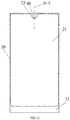
- the display panel 20 may include a display region 21 for displaying information and a non-display region 22 that is not configured to display information.
- the display region 21 can serve as a main display region of the display panel 20 for displaying most of the information.
- the non-display region 22 may be disposed outside the display region 21.
- the non-display region 22 can be configured to receive an Integrated Circuit (IC).
- the IC is configured to control the information displayed by the display panel 20.
- the shielding region 12 of the cover 10 can be disposed in front of the non-display region 22 of the display panel 20. Such that the non-display region 22 of the display panel 20 is hidden.
- the display panel 20 may include a functional region 23.
- the at least two functional modules 60 can be at least partially received in the functional region 23.
- the functional region 23 may be defined in a structure of a hole, but the embodiments of the functional region are not limited thereto.
- the functional region 23 may have a shape of a circular arc, a rounded rectangle, a rounded square, etc.
- the functional region 23 can be defined in the display region 21 of the display panel 20.
- a location of the functional region 23 may be changed according to the functions performed by the at least two functional modules 60 and the location of the at least two functional modules 60.
- the at least two functional modules 60 include a sensor module 61 and a camera 62.
- the sensor module 61 is juxtaposed with the camera 62.
- the sensor module 61 is disposed at one side of the camera 62, such as a left side of the camera 62. It can be understood that the sensor module 61 can be disposed above the camera 62.
- the sensor module is 61 an integrative module of two components.
- the sensor module 61 is an integrative module of a signal receiver and a signal emitter.
- the sensor module 61 is not an integrative module of two components, that is, the sensor module 61 includes a signal receiver 611 and a signal emitter 612.
- the signal receiver 611 and the signal emitter 612 are spaced apart from each other. A distance between the signal receiver 611 and the signal emitter 612 ranges from 6 mm to 14 mm.
- the signal receiver 611 is juxtaposed with the signal emitter 612.
- the signal receiver 611 and the signal emitter 612 are disposed at opposite sides of the camera 62.
- the signal receiver 611 and the signal emitter 612 are respectively disposed at left and right sides of the camera 62. It can be understood that the signal receiver 611 and the signal emitter 612 can be respectively disposed at upper and lower sides of the camera 62.
- the camera 62 includes a lens 621 and a base 622.
- the base 622 and the lens 621 cooperatively form a step 623, that is, the base 622 and the lens 621 cooperatively form an invert T-shaped structure.
- a portion on where the lens 621 is located is a protruding portion of the invert T-shaped structure, and a portion located on opposite sides of the lens 621 is the step 623 of the invert T-shaped structure.
- the signal receiver 611 and the signal emitter 612 are disposed on the step 623, that is, the signal receiver 611 and the signal emitter 612 are located on stepped structures that are located on left and right sides of the invert T-shaped structure. It can be understood that the step 623 may not be formed by the base 622 and the lens 621, and the camera 62 may be directly disposed as a T-shaped structure.
- the signal receiver 611 can be juxtaposed with the signal emitter 612, and both of the signal receiver 611 and the signal emitter 612 can be disposed above the camera 62.
- the signal receiver 611 and the signal emitter 612 are located on the step 623 of the camera 62 that closed to the signal receiver 611 and the signal emitter 612.
- the at least two functional modules 60 further include a telephone receiver 63.
- the telephone receiver 63 is disposed above the sensor module 61 and the camera 62. In an embodiment, a top portion of the telephone receiver 63 is flush with a top portion of the camera 62. In order to reduce a size of the functional region, the telephone receiver 63 is disposed at an edge of the display panel 20, i.e., the telephone receiver 63 is disposed at a top edge closed to the housing 40. It can be understood that the telephone receiver 63 can also be disposed below the sensor module 61 and the camera 62. In an embodiment, the camera 62 is juxtaposed with the sensor module 61.
- the sensor module 61 is disposed between the telephone receiver 63 and the camera 62.
- the signal receiver 611 and the signal emitter 612 are disposed between the telephone receiver 63 and the camera 62.
- the sensor module 61 further includes an ambient light sensor 613.
- the signal receiver 611 and the ambient light sensor 613 are integrated with each other.
- the display panel 20 may not include any non-display region, that is, the display panel 20 may include only the display region 21 and the functional region 23.
- the IC for controlling the information displayed by the display panel 20 may be disposed along a direction of a thickness of the display panel 20.
- FIG. 12 illustrates a cross-sectional view of the display panel 20 of FIG. 11 , taken along a line PI-PI.
- the display panel 20 may include a number of layers.
- display panel 20 may include an upper plate 24 and a lower plate 25.
- the upper plate 24 may include a color filter layer.
- the lower plate 25 may include a thin film transistor and electronic cables coupled to the thin film transistor.
- a liquid crystal layer may be disposed between the upper plate 24 and the lower plate 25.
- components of the layers of the display panel 20 are not limited thereto, but may be changed according to a type of the display panel 20.
- a liquid crystal layer disposed between the upper plate 24 and the lower plate 25 may be omitted, or an organic/inorganic material layer may be formed between the upper plate 24 and the lower plate 25.
- the functional region 23 can be defined in the upper plate 24 and/or the lower plate 25 of the display panel 20.
- the functional region 23 may be a blind hole when defined in the upper plate 24 or the lower plate 25 of the display panel 20.
- the functional region 23 may be a through hole when defined in the upper plate 24 and the lower plate 25 of the display panel 20.
- the at least two functional modules 60 can be at least partially received in the functional region 23. For example, some portions of the at least two functional modules 60 can be partially received in the functional region 23 in terms of size; and in terms of thickness, some portions of the at least two functional modules 60 can be partially received in the functional region 23.
- At least some portions of the at least two functional modules 60 are partially received in the functional region 23 of the display panel 20.
- a thickness of the at least two functional modules 60 is labeled as d1
- a thickness of the display panel 20 is labeled as d2.
- a size (or an area) of the at least two functional modules 60 and the display panel 20 may also be smaller than the sum of their original sizes (or areas), when the at least two functional modules 60 and the display panel 20 are coupled to each other in the terminal 100.
- a thickness of the functional modules 60 and the display panel 20 while mounted to the terminal 100 may be the equal to the thickness d1 of the functional modules 60.
- the thickness d2 of the functional modules 60 when the functional modules 60 are overlapped with the display panel 20 via the functional region 23 does not result in an increase in a thickness of the terminal 100.
- a shaped of the projection contour of the functional region 23 may be selected from a circular arc, a rounded rectangular, a rounded square, a circular, or other shapes.
- the projection contour refers to a contour of the functional region 23 when projected in a direction perpendicular to the front surface.
- a shaped of the projection contour of the functional region 23 may be changed according to the shape of the functional modules 60 partially received in the functional region 23, and the ratio in which the functional modules 60 are partially received in the functional region 23.
- the projection contour of the functional region 23 may have a shape of semi-circular (i.e. a circular arc shape). That is, a projection contour of the functional modules 60 is half of the projection contour of the functional modules 60.
- the projection contour of the functional regions 23 may have a shape of square corresponding to the projection contour of the functional modules 60, which has a shape of square.
- the functional modules 60 described above is disposed at an edge of the middle of a top end or at an edge of the middle of a bottom end, and the functional region 23 may also be disposed at an edge of the top or bottom middle portion, which is not intended to limit the disclosure. It can be understood that the functional modules 60 can also be disposed in the middle of the top end of the terminal, and the functional region 23 can be located in the middle of the top end of the display region 21. Of course, it is not limited to the above, for example, the functional region 23 may be disposed inside the display panel as long as the functional modules 60 are corresponding to the functional region 23.
- the functional region 23 can be defined by a variety of ways. In some embodiments, the functional region 23 can be defined by cutting via a blade. In some embodiments, the functional region 23 can be defined by laser cutting.
- FIG. 15 illustrates a cross-sectional view of an example of how the functional modules 60 are disposed in the terminal 100.
- the cover 10 may be disposed in front of the housing 40.
- the display panel 20, the printed circuit board 30, the battery 50, and the functional modules 60 can be disposed between housing 40 and cover 10.
- the functional modules 60 further include a signal receiving region 614.
- the signal receiving region 614 is configured to transmit a signal captured by the functional modules 60 to a signal processor of the printed circuit, from outside.
- the functional modules 60 that are partially received in the functional region 23 include a camera 62 and a sensor module 61.
- the functional modules 60 that are partially received in the functional region 23 include a camera 62 and a telephone receiver 63.
- the functional modules 60 that are partially received in the functional region 23 include a camera 62, a telephone receiver 63, and a sensor module 61.
- a number of the functional modules 60 may be three or more, which is not repeated therein.
- two functional modules 60a and 60b respectively disposed on a front side and a rear side of the terminal 100 are partially received in a front side and a rear side of the functional region 23, respectively.
- the functional module 60a disposed on the front side may be a camera module
- the functional module 60b disposed on the rear side may be a heart rate sensor module for detecting heart rate.
- the two functional modules 60a and 60b are juxtaposed in one functional region 23 of the display panel 20.
- the functional module 60a may be a camera module
- the functional module 60b may be a proximity sensor module for detecting a distance between the terminal and an external object.
- the functional modules 60 partially received in the functional region 23 can pass through the housing 40.
- the functional modules 60 provide a first region 601 and a second region 602 that are disposed opposite to each other.
- the first region 601 and the second region 602 are respectively configured to perform different functions.
- the first region 601 can perform a display function for displaying information in conjunction with the display region of the display panel 20.
- the second region 602 can be configured to perform functions of a camera, or functions of a heart rate sensor, and the like.
- the functional modules 60 can also be partially received in the functional region 23 by rotating.
- the functional modules 60 provide a first region and a second region opposite to each other.
- the functional modules 60 can be rotated about an axis I-I of the terminal, thereby the first region is located on a surface on which the display panel 20 is disposed; or the functional modules 60 can be rotated at 180 degrees about the axis I-I thereby the second region is located on a surface on which the display panel 20 is disposed.
- the axis I-I is parallel to a line along which an upper end of the display panel 20 is disposed.
- the functional modules 60 can also be partially received in the functional region 23 by rotating.
- the functional modules 60 provide a first region and a second region opposite to each other.
- the functional modules 60 can be rotated about an axis II-II of the terminal, thereby the first region is located on a surface on which the display panel 20 is disposed; or the functional modules 60 can be rotated at 180 degrees about the axis II-II thereby the second region is located on a surface on which the display panel 20 is disposed.
- the axis II-II is parallel to a line along which a side edge of the display panel 20 is disposed.
- the functional modules 60 can have multiple modes of operation.
- the functional modules 60 can perform functions of a camera and a displayer.
- the functional modules 60 can serve as a sub-display region for cooperating with the display region of the display panel 20 to display information.
- the functional modules 60 are configured to perform a shooting function.
- the terminal defines a functional region in the display panel.
- the functional region is configured to receive at least two functional modules selected from modules such as a camera, a telephone receiver, and a sensor.
- modules such as a camera, a telephone receiver, and a sensor.
- an area of the functional region is reduced, compared with original terminals. That is, an area of the non-display region is reduced.
- the display region can have a larger size. Thereby displaying with a larger size of the display panel can be achieved.
Landscapes
- Engineering & Computer Science (AREA)
- Computer Hardware Design (AREA)
- Theoretical Computer Science (AREA)
- Human Computer Interaction (AREA)
- Physics & Mathematics (AREA)
- General Engineering & Computer Science (AREA)
- General Physics & Mathematics (AREA)
- Microelectronics & Electronic Packaging (AREA)
- Signal Processing (AREA)
- Devices For Indicating Variable Information By Combining Individual Elements (AREA)
- Telephone Set Structure (AREA)
Applications Claiming Priority (3)
| Application Number | Priority Date | Filing Date | Title |
|---|---|---|---|
| CN201710132542.8A CN106940584B (zh) | 2017-03-07 | 2017-03-07 | 终端 |
| CN201720218878.1U CN206930978U (zh) | 2017-03-07 | 2017-03-07 | 终端 |
| PCT/CN2018/076016 WO2018161778A1 (zh) | 2017-03-07 | 2018-02-09 | 终端 |
Publications (3)
| Publication Number | Publication Date |
|---|---|
| EP3582062A1 true EP3582062A1 (de) | 2019-12-18 |
| EP3582062A4 EP3582062A4 (de) | 2020-02-26 |
| EP3582062B1 EP3582062B1 (de) | 2021-04-07 |
Family
ID=63448042
Family Applications (1)
| Application Number | Title | Priority Date | Filing Date |
|---|---|---|---|
| EP18763039.7A Active EP3582062B1 (de) | 2017-03-07 | 2018-02-09 | Endgerät |
Country Status (3)
| Country | Link |
|---|---|
| US (1) | US10855823B2 (de) |
| EP (1) | EP3582062B1 (de) |
| WO (1) | WO2018161778A1 (de) |
Families Citing this family (4)
| Publication number | Priority date | Publication date | Assignee | Title |
|---|---|---|---|---|
| JP1638211S (de) | 2018-05-03 | 2019-08-05 | ||
| CN108845445A (zh) * | 2018-08-24 | 2018-11-20 | 武汉华星光电技术有限公司 | 全面显示屏及采用该全面显示屏的显示装置 |
| CN110618549B (zh) * | 2018-12-03 | 2024-10-29 | 鸿富锦精密工业(深圳)有限公司 | 显示装置 |
| WO2021203329A1 (zh) * | 2020-04-08 | 2021-10-14 | 京东方科技集团股份有限公司 | 显示基板及其制备方法、显示装置 |
Family Cites Families (24)
| Publication number | Priority date | Publication date | Assignee | Title |
|---|---|---|---|---|
| JP2000299727A (ja) * | 1999-04-13 | 2000-10-24 | Nec Corp | 通信装置および携帯無線通信装置 |
| US9894781B2 (en) * | 2012-06-06 | 2018-02-13 | Apple Inc. | Notched display layers |
| KR101397084B1 (ko) * | 2012-07-02 | 2014-05-20 | 엘지전자 주식회사 | 이동 단말기 |
| KR101992189B1 (ko) * | 2012-09-19 | 2019-06-24 | 엘지전자 주식회사 | 이동 단말기 및 그 제어방법 |
| KR101847075B1 (ko) * | 2014-12-18 | 2018-04-09 | 삼성전자주식회사 | 전자 장치 |
| US10320101B2 (en) * | 2015-06-10 | 2019-06-11 | Fairphone B.V. | Connector for an electronic device |
| EP3104250A1 (de) * | 2015-06-10 | 2016-12-14 | FairPhone B.V. | Elektronische vorrichtung |
| CN106293444B (zh) * | 2015-06-25 | 2020-07-03 | 小米科技有限责任公司 | 移动终端、显示控制方法及装置 |
| KR102448304B1 (ko) * | 2016-02-04 | 2022-09-28 | 삼성전자 주식회사 | 금속 하우징을 포함하는 전자 장치 |
| KR102489948B1 (ko) * | 2016-02-18 | 2023-01-19 | 삼성전자주식회사 | 전자 장치 및 전자 장치 제조방법 |
| CN205610701U (zh) * | 2016-04-07 | 2016-09-28 | 广东欧珀移动通信有限公司 | 移动终端 |
| KR102516344B1 (ko) * | 2016-06-21 | 2023-04-03 | 삼성전자주식회사 | 커버 윈도우 및 이를 포함하는 전자 장치 |
| WO2018006427A1 (zh) * | 2016-07-08 | 2018-01-11 | 华为技术有限公司 | 一种电池盖以及电子设备 |
| CN106412159A (zh) * | 2016-10-26 | 2017-02-15 | 广东欧珀移动通信有限公司 | 一种面板、面板组件及终端 |
| CN106453722A (zh) * | 2016-11-30 | 2017-02-22 | 努比亚技术有限公司 | 一种听筒装置及移动终端 |
| CN106453726B (zh) * | 2016-12-06 | 2022-10-21 | Oppo广东移动通信有限公司 | 传感器组件及终端 |
| KR20180098466A (ko) * | 2017-02-25 | 2018-09-04 | 삼성전자주식회사 | 코너가 둥근 디스플레이를 구비한 전자 장치 |
| CN106940584B (zh) * | 2017-03-07 | 2023-07-14 | Oppo广东移动通信有限公司 | 终端 |
| CN206930978U (zh) * | 2017-03-07 | 2018-01-26 | 广东欧珀移动通信有限公司 | 终端 |
| CN107248374B (zh) * | 2017-06-30 | 2021-04-09 | 厦门天马微电子有限公司 | 显示屏及显示装置 |
| CN107331314A (zh) * | 2017-08-23 | 2017-11-07 | 京东方科技集团股份有限公司 | 一种显示装置 |
| KR102503420B1 (ko) * | 2018-01-02 | 2023-02-24 | 삼성전자주식회사 | 탄성을 가지는 커넥터를 포함하는 카메라 모듈 및 이를 구비한 모바일 장치 |
| CN108111650B (zh) * | 2018-01-10 | 2020-07-03 | 北京小米移动软件有限公司 | Lcd显示模组及移动终端 |
| KR102646718B1 (ko) * | 2018-11-16 | 2024-03-14 | 삼성디스플레이 주식회사 | 전자장치 |
-
2018
- 2018-02-09 EP EP18763039.7A patent/EP3582062B1/de active Active
- 2018-02-09 WO PCT/CN2018/076016 patent/WO2018161778A1/zh not_active Ceased
-
2019
- 2019-09-06 US US16/563,037 patent/US10855823B2/en active Active
Also Published As
| Publication number | Publication date |
|---|---|
| US10855823B2 (en) | 2020-12-01 |
| US20190394318A1 (en) | 2019-12-26 |
| WO2018161778A1 (zh) | 2018-09-13 |
| EP3582062B1 (de) | 2021-04-07 |
| EP3582062A4 (de) | 2020-02-26 |
Similar Documents
| Publication | Publication Date | Title |
|---|---|---|
| CN106850897B (zh) | 终端 | |
| US10615239B2 (en) | Integration of display screen and optical fingerprint sensor | |
| CN106940584B (zh) | 终端 | |
| CN106774689B (zh) | 显示屏、显示屏组件及终端 | |
| US10739824B2 (en) | Electronic device | |
| EP3987758B1 (de) | Elektronische vorrichtung mit kameramodul | |
| JP6786723B2 (ja) | 機能アセンブリ、表示装置、及び端末 | |
| EP3373562A1 (de) | Endgerät mit kameramodul | |
| US10855823B2 (en) | Terminal | |
| KR101969801B1 (ko) | 이동 단말기 | |
| KR102409855B1 (ko) | 윈도우 부재 및 이를 포함하는 표시 장치 | |
| CN107046588B (zh) | 显示组件及移动终端 | |
| CN110543043A (zh) | 显示屏及电子设备 | |
| CN206559422U (zh) | 一种终端 | |
| CN206930978U (zh) | 终端 | |
| US12069194B2 (en) | Display panel and electronic device | |
| CN206930980U (zh) | 显示屏、显示屏组件及终端 | |
| US10841469B2 (en) | Image module and electronic device | |
| US10073497B1 (en) | Display device | |
| HK1236646A1 (en) | Display screen, display screen assembly, and terminal | |
| HK1236646A (en) | Display screen, display screen assembly, and terminal | |
| WO2024221362A1 (zh) | 摄像头组件、显示设备及其组装方法 | |
| HK1236646B (zh) | 显示屏、显示屏组件及终端 | |
| JP2014235208A (ja) | 表示装置を搭載する電子機器 |
Legal Events
| Date | Code | Title | Description |
|---|---|---|---|
| STAA | Information on the status of an ep patent application or granted ep patent |
Free format text: STATUS: THE INTERNATIONAL PUBLICATION HAS BEEN MADE |
|
| PUAI | Public reference made under article 153(3) epc to a published international application that has entered the european phase |
Free format text: ORIGINAL CODE: 0009012 |
|
| STAA | Information on the status of an ep patent application or granted ep patent |
Free format text: STATUS: REQUEST FOR EXAMINATION WAS MADE |
|
| 17P | Request for examination filed |
Effective date: 20190913 |
|
| AK | Designated contracting states |
Kind code of ref document: A1 Designated state(s): AL AT BE BG CH CY CZ DE DK EE ES FI FR GB GR HR HU IE IS IT LI LT LU LV MC MK MT NL NO PL PT RO RS SE SI SK SM TR |
|
| AX | Request for extension of the european patent |
Extension state: BA ME |
|
| A4 | Supplementary search report drawn up and despatched |
Effective date: 20200129 |
|
| RIC1 | Information provided on ipc code assigned before grant |
Ipc: G06F 1/16 20060101AFI20200123BHEP |
|
| DAV | Request for validation of the european patent (deleted) | ||
| DAX | Request for extension of the european patent (deleted) | ||
| GRAP | Despatch of communication of intention to grant a patent |
Free format text: ORIGINAL CODE: EPIDOSNIGR1 |
|
| STAA | Information on the status of an ep patent application or granted ep patent |
Free format text: STATUS: GRANT OF PATENT IS INTENDED |
|
| INTG | Intention to grant announced |
Effective date: 20201103 |
|
| GRAS | Grant fee paid |
Free format text: ORIGINAL CODE: EPIDOSNIGR3 |
|
| GRAA | (expected) grant |
Free format text: ORIGINAL CODE: 0009210 |
|
| STAA | Information on the status of an ep patent application or granted ep patent |
Free format text: STATUS: THE PATENT HAS BEEN GRANTED |
|
| AK | Designated contracting states |
Kind code of ref document: B1 Designated state(s): AL AT BE BG CH CY CZ DE DK EE ES FI FR GB GR HR HU IE IS IT LI LT LU LV MC MK MT NL NO PL PT RO RS SE SI SK SM TR |
|
| REG | Reference to a national code |
Ref country code: GB Ref legal event code: FG4D |
|
| REG | Reference to a national code |
Ref country code: AT Ref legal event code: REF Ref document number: 1380539 Country of ref document: AT Kind code of ref document: T Effective date: 20210415 Ref country code: CH Ref legal event code: EP |
|
| REG | Reference to a national code |
Ref country code: DE Ref legal event code: R096 Ref document number: 602018015319 Country of ref document: DE |
|
| REG | Reference to a national code |
Ref country code: IE Ref legal event code: FG4D |
|
| REG | Reference to a national code |
Ref country code: LT Ref legal event code: MG9D |
|
| REG | Reference to a national code |
Ref country code: NL Ref legal event code: MP Effective date: 20210407 Ref country code: AT Ref legal event code: MK05 Ref document number: 1380539 Country of ref document: AT Kind code of ref document: T Effective date: 20210407 |
|
| PG25 | Lapsed in a contracting state [announced via postgrant information from national office to epo] |
Ref country code: LT Free format text: LAPSE BECAUSE OF FAILURE TO SUBMIT A TRANSLATION OF THE DESCRIPTION OR TO PAY THE FEE WITHIN THE PRESCRIBED TIME-LIMIT Effective date: 20210407 Ref country code: HR Free format text: LAPSE BECAUSE OF FAILURE TO SUBMIT A TRANSLATION OF THE DESCRIPTION OR TO PAY THE FEE WITHIN THE PRESCRIBED TIME-LIMIT Effective date: 20210407 Ref country code: FI Free format text: LAPSE BECAUSE OF FAILURE TO SUBMIT A TRANSLATION OF THE DESCRIPTION OR TO PAY THE FEE WITHIN THE PRESCRIBED TIME-LIMIT Effective date: 20210407 Ref country code: NL Free format text: LAPSE BECAUSE OF FAILURE TO SUBMIT A TRANSLATION OF THE DESCRIPTION OR TO PAY THE FEE WITHIN THE PRESCRIBED TIME-LIMIT Effective date: 20210407 Ref country code: AT Free format text: LAPSE BECAUSE OF FAILURE TO SUBMIT A TRANSLATION OF THE DESCRIPTION OR TO PAY THE FEE WITHIN THE PRESCRIBED TIME-LIMIT Effective date: 20210407 Ref country code: BG Free format text: LAPSE BECAUSE OF FAILURE TO SUBMIT A TRANSLATION OF THE DESCRIPTION OR TO PAY THE FEE WITHIN THE PRESCRIBED TIME-LIMIT Effective date: 20210707 |
|
| PG25 | Lapsed in a contracting state [announced via postgrant information from national office to epo] |
Ref country code: PL Free format text: LAPSE BECAUSE OF FAILURE TO SUBMIT A TRANSLATION OF THE DESCRIPTION OR TO PAY THE FEE WITHIN THE PRESCRIBED TIME-LIMIT Effective date: 20210407 Ref country code: NO Free format text: LAPSE BECAUSE OF FAILURE TO SUBMIT A TRANSLATION OF THE DESCRIPTION OR TO PAY THE FEE WITHIN THE PRESCRIBED TIME-LIMIT Effective date: 20210707 Ref country code: LV Free format text: LAPSE BECAUSE OF FAILURE TO SUBMIT A TRANSLATION OF THE DESCRIPTION OR TO PAY THE FEE WITHIN THE PRESCRIBED TIME-LIMIT Effective date: 20210407 Ref country code: SE Free format text: LAPSE BECAUSE OF FAILURE TO SUBMIT A TRANSLATION OF THE DESCRIPTION OR TO PAY THE FEE WITHIN THE PRESCRIBED TIME-LIMIT Effective date: 20210407 Ref country code: PT Free format text: LAPSE BECAUSE OF FAILURE TO SUBMIT A TRANSLATION OF THE DESCRIPTION OR TO PAY THE FEE WITHIN THE PRESCRIBED TIME-LIMIT Effective date: 20210809 Ref country code: RS Free format text: LAPSE BECAUSE OF FAILURE TO SUBMIT A TRANSLATION OF THE DESCRIPTION OR TO PAY THE FEE WITHIN THE PRESCRIBED TIME-LIMIT Effective date: 20210407 Ref country code: GR Free format text: LAPSE BECAUSE OF FAILURE TO SUBMIT A TRANSLATION OF THE DESCRIPTION OR TO PAY THE FEE WITHIN THE PRESCRIBED TIME-LIMIT Effective date: 20210708 Ref country code: IS Free format text: LAPSE BECAUSE OF FAILURE TO SUBMIT A TRANSLATION OF THE DESCRIPTION OR TO PAY THE FEE WITHIN THE PRESCRIBED TIME-LIMIT Effective date: 20210807 |
|
| REG | Reference to a national code |
Ref country code: DE Ref legal event code: R097 Ref document number: 602018015319 Country of ref document: DE |
|
| PG25 | Lapsed in a contracting state [announced via postgrant information from national office to epo] |
Ref country code: SK Free format text: LAPSE BECAUSE OF FAILURE TO SUBMIT A TRANSLATION OF THE DESCRIPTION OR TO PAY THE FEE WITHIN THE PRESCRIBED TIME-LIMIT Effective date: 20210407 Ref country code: EE Free format text: LAPSE BECAUSE OF FAILURE TO SUBMIT A TRANSLATION OF THE DESCRIPTION OR TO PAY THE FEE WITHIN THE PRESCRIBED TIME-LIMIT Effective date: 20210407 Ref country code: ES Free format text: LAPSE BECAUSE OF FAILURE TO SUBMIT A TRANSLATION OF THE DESCRIPTION OR TO PAY THE FEE WITHIN THE PRESCRIBED TIME-LIMIT Effective date: 20210407 Ref country code: SM Free format text: LAPSE BECAUSE OF FAILURE TO SUBMIT A TRANSLATION OF THE DESCRIPTION OR TO PAY THE FEE WITHIN THE PRESCRIBED TIME-LIMIT Effective date: 20210407 Ref country code: RO Free format text: LAPSE BECAUSE OF FAILURE TO SUBMIT A TRANSLATION OF THE DESCRIPTION OR TO PAY THE FEE WITHIN THE PRESCRIBED TIME-LIMIT Effective date: 20210407 Ref country code: DK Free format text: LAPSE BECAUSE OF FAILURE TO SUBMIT A TRANSLATION OF THE DESCRIPTION OR TO PAY THE FEE WITHIN THE PRESCRIBED TIME-LIMIT Effective date: 20210407 Ref country code: CZ Free format text: LAPSE BECAUSE OF FAILURE TO SUBMIT A TRANSLATION OF THE DESCRIPTION OR TO PAY THE FEE WITHIN THE PRESCRIBED TIME-LIMIT Effective date: 20210407 |
|
| PLBE | No opposition filed within time limit |
Free format text: ORIGINAL CODE: 0009261 |
|
| STAA | Information on the status of an ep patent application or granted ep patent |
Free format text: STATUS: NO OPPOSITION FILED WITHIN TIME LIMIT |
|
| 26N | No opposition filed |
Effective date: 20220110 |
|
| PG25 | Lapsed in a contracting state [announced via postgrant information from national office to epo] |
Ref country code: IS Free format text: LAPSE BECAUSE OF FAILURE TO SUBMIT A TRANSLATION OF THE DESCRIPTION OR TO PAY THE FEE WITHIN THE PRESCRIBED TIME-LIMIT Effective date: 20210807 Ref country code: AL Free format text: LAPSE BECAUSE OF FAILURE TO SUBMIT A TRANSLATION OF THE DESCRIPTION OR TO PAY THE FEE WITHIN THE PRESCRIBED TIME-LIMIT Effective date: 20210407 |
|
| PG25 | Lapsed in a contracting state [announced via postgrant information from national office to epo] |
Ref country code: IT Free format text: LAPSE BECAUSE OF FAILURE TO SUBMIT A TRANSLATION OF THE DESCRIPTION OR TO PAY THE FEE WITHIN THE PRESCRIBED TIME-LIMIT Effective date: 20210407 |
|
| PG25 | Lapsed in a contracting state [announced via postgrant information from national office to epo] |
Ref country code: MC Free format text: LAPSE BECAUSE OF FAILURE TO SUBMIT A TRANSLATION OF THE DESCRIPTION OR TO PAY THE FEE WITHIN THE PRESCRIBED TIME-LIMIT Effective date: 20210407 |
|
| REG | Reference to a national code |
Ref country code: CH Ref legal event code: PL |
|
| REG | Reference to a national code |
Ref country code: BE Ref legal event code: MM Effective date: 20220228 |
|
| PG25 | Lapsed in a contracting state [announced via postgrant information from national office to epo] |
Ref country code: LU Free format text: LAPSE BECAUSE OF NON-PAYMENT OF DUE FEES Effective date: 20220209 |
|
| PG25 | Lapsed in a contracting state [announced via postgrant information from national office to epo] |
Ref country code: LI Free format text: LAPSE BECAUSE OF NON-PAYMENT OF DUE FEES Effective date: 20220228 Ref country code: IE Free format text: LAPSE BECAUSE OF NON-PAYMENT OF DUE FEES Effective date: 20220209 Ref country code: CH Free format text: LAPSE BECAUSE OF NON-PAYMENT OF DUE FEES Effective date: 20220228 |
|
| PG25 | Lapsed in a contracting state [announced via postgrant information from national office to epo] |
Ref country code: BE Free format text: LAPSE BECAUSE OF NON-PAYMENT OF DUE FEES Effective date: 20220228 |
|
| P01 | Opt-out of the competence of the unified patent court (upc) registered |
Effective date: 20230412 |
|
| PG25 | Lapsed in a contracting state [announced via postgrant information from national office to epo] |
Ref country code: MK Free format text: LAPSE BECAUSE OF FAILURE TO SUBMIT A TRANSLATION OF THE DESCRIPTION OR TO PAY THE FEE WITHIN THE PRESCRIBED TIME-LIMIT Effective date: 20210407 Ref country code: CY Free format text: LAPSE BECAUSE OF FAILURE TO SUBMIT A TRANSLATION OF THE DESCRIPTION OR TO PAY THE FEE WITHIN THE PRESCRIBED TIME-LIMIT Effective date: 20210407 |
|
| PG25 | Lapsed in a contracting state [announced via postgrant information from national office to epo] |
Ref country code: HU Free format text: LAPSE BECAUSE OF FAILURE TO SUBMIT A TRANSLATION OF THE DESCRIPTION OR TO PAY THE FEE WITHIN THE PRESCRIBED TIME-LIMIT; INVALID AB INITIO Effective date: 20180209 |
|
| PG25 | Lapsed in a contracting state [announced via postgrant information from national office to epo] |
Ref country code: MT Free format text: LAPSE BECAUSE OF FAILURE TO SUBMIT A TRANSLATION OF THE DESCRIPTION OR TO PAY THE FEE WITHIN THE PRESCRIBED TIME-LIMIT Effective date: 20210407 |
|
| PG25 | Lapsed in a contracting state [announced via postgrant information from national office to epo] |
Ref country code: TR Free format text: LAPSE BECAUSE OF FAILURE TO SUBMIT A TRANSLATION OF THE DESCRIPTION OR TO PAY THE FEE WITHIN THE PRESCRIBED TIME-LIMIT Effective date: 20210407 |
|
| PGFP | Annual fee paid to national office [announced via postgrant information from national office to epo] |
Ref country code: GB Payment date: 20260224 Year of fee payment: 9 |
|
| PGFP | Annual fee paid to national office [announced via postgrant information from national office to epo] |
Ref country code: DE Payment date: 20260223 Year of fee payment: 9 |
|
| PGFP | Annual fee paid to national office [announced via postgrant information from national office to epo] |
Ref country code: FR Payment date: 20260224 Year of fee payment: 9 |