EP3584842A1 - Anzeigebildschirm, anzeigevorrichtung und mobiles endgerät - Google Patents
Anzeigebildschirm, anzeigevorrichtung und mobiles endgerät Download PDFInfo
- Publication number
- EP3584842A1 EP3584842A1 EP18790395.0A EP18790395A EP3584842A1 EP 3584842 A1 EP3584842 A1 EP 3584842A1 EP 18790395 A EP18790395 A EP 18790395A EP 3584842 A1 EP3584842 A1 EP 3584842A1
- Authority
- EP
- European Patent Office
- Prior art keywords
- transparent
- display screen
- thin film
- fingerprint recognition
- data lines
- Prior art date
- Legal status (The legal status is an assumption and is not a legal conclusion. Google has not performed a legal analysis and makes no representation as to the accuracy of the status listed.)
- Granted
Links
Images




Classifications
-
- G—PHYSICS
- G06—COMPUTING OR CALCULATING; COUNTING
- G06V—IMAGE OR VIDEO RECOGNITION OR UNDERSTANDING
- G06V40/00—Recognition of biometric, human-related or animal-related patterns in image or video data
- G06V40/10—Human or animal bodies, e.g. vehicle occupants or pedestrians; Body parts, e.g. hands
- G06V40/12—Fingerprints or palmprints
- G06V40/13—Sensors therefor
- G06V40/1318—Sensors therefor using electro-optical elements or layers, e.g. electroluminescent sensing
-
- G—PHYSICS
- G09—EDUCATION; CRYPTOGRAPHY; DISPLAY; ADVERTISING; SEALS
- G09G—ARRANGEMENTS OR CIRCUITS FOR CONTROL OF INDICATING DEVICES USING STATIC MEANS TO PRESENT VARIABLE INFORMATION
- G09G3/00—Control arrangements or circuits, of interest only in connection with visual indicators other than cathode-ray tubes
- G09G3/20—Control arrangements or circuits, of interest only in connection with visual indicators other than cathode-ray tubes for presentation of an assembly of a number of characters, e.g. a page, by composing the assembly by combination of individual elements arranged in a matrix no fixed position being assigned to or needed to be assigned to the individual characters or partial characters
- G09G3/22—Control arrangements or circuits, of interest only in connection with visual indicators other than cathode-ray tubes for presentation of an assembly of a number of characters, e.g. a page, by composing the assembly by combination of individual elements arranged in a matrix no fixed position being assigned to or needed to be assigned to the individual characters or partial characters using controlled light sources
- G09G3/30—Control arrangements or circuits, of interest only in connection with visual indicators other than cathode-ray tubes for presentation of an assembly of a number of characters, e.g. a page, by composing the assembly by combination of individual elements arranged in a matrix no fixed position being assigned to or needed to be assigned to the individual characters or partial characters using controlled light sources using electroluminescent panels
- G09G3/32—Control arrangements or circuits, of interest only in connection with visual indicators other than cathode-ray tubes for presentation of an assembly of a number of characters, e.g. a page, by composing the assembly by combination of individual elements arranged in a matrix no fixed position being assigned to or needed to be assigned to the individual characters or partial characters using controlled light sources using electroluminescent panels semiconductive, e.g. using light-emitting diodes [LED]
- G09G3/3208—Control arrangements or circuits, of interest only in connection with visual indicators other than cathode-ray tubes for presentation of an assembly of a number of characters, e.g. a page, by composing the assembly by combination of individual elements arranged in a matrix no fixed position being assigned to or needed to be assigned to the individual characters or partial characters using controlled light sources using electroluminescent panels semiconductive, e.g. using light-emitting diodes [LED] organic, e.g. using organic light-emitting diodes [OLED]
- G09G3/3225—Control arrangements or circuits, of interest only in connection with visual indicators other than cathode-ray tubes for presentation of an assembly of a number of characters, e.g. a page, by composing the assembly by combination of individual elements arranged in a matrix no fixed position being assigned to or needed to be assigned to the individual characters or partial characters using controlled light sources using electroluminescent panels semiconductive, e.g. using light-emitting diodes [LED] organic, e.g. using organic light-emitting diodes [OLED] using an active matrix
-
- G—PHYSICS
- G06—COMPUTING OR CALCULATING; COUNTING
- G06V—IMAGE OR VIDEO RECOGNITION OR UNDERSTANDING
- G06V10/00—Arrangements for image or video recognition or understanding
- G06V10/10—Image acquisition
- G06V10/12—Details of acquisition arrangements; Constructional details thereof
- G06V10/14—Optical characteristics of the device performing the acquisition or on the illumination arrangements
- G06V10/147—Details of sensors, e.g. sensor lenses
-
- H—ELECTRICITY
- H10—SEMICONDUCTOR DEVICES; ELECTRIC SOLID-STATE DEVICES NOT OTHERWISE PROVIDED FOR
- H10D—INORGANIC ELECTRIC SEMICONDUCTOR DEVICES
- H10D30/00—Field-effect transistors [FET]
- H10D30/60—Insulated-gate field-effect transistors [IGFET]
- H10D30/67—Thin-film transistors [TFT]
-
- H—ELECTRICITY
- H10—SEMICONDUCTOR DEVICES; ELECTRIC SOLID-STATE DEVICES NOT OTHERWISE PROVIDED FOR
- H10D—INORGANIC ELECTRIC SEMICONDUCTOR DEVICES
- H10D30/00—Field-effect transistors [FET]
- H10D30/60—Insulated-gate field-effect transistors [IGFET]
- H10D30/67—Thin-film transistors [TFT]
- H10D30/6729—Thin-film transistors [TFT] characterised by the electrodes
- H10D30/6737—Thin-film transistors [TFT] characterised by the electrodes characterised by the electrode materials
- H10D30/6739—Conductor-insulator-semiconductor electrodes
-
- H—ELECTRICITY
- H10—SEMICONDUCTOR DEVICES; ELECTRIC SOLID-STATE DEVICES NOT OTHERWISE PROVIDED FOR
- H10D—INORGANIC ELECTRIC SEMICONDUCTOR DEVICES
- H10D64/00—Electrodes of devices having potential barriers
- H10D64/60—Electrodes characterised by their materials
-
- H—ELECTRICITY
- H10—SEMICONDUCTOR DEVICES; ELECTRIC SOLID-STATE DEVICES NOT OTHERWISE PROVIDED FOR
- H10D—INORGANIC ELECTRIC SEMICONDUCTOR DEVICES
- H10D64/00—Electrodes of devices having potential barriers
- H10D64/60—Electrodes characterised by their materials
- H10D64/62—Electrodes ohmically coupled to a semiconductor
-
- H—ELECTRICITY
- H10—SEMICONDUCTOR DEVICES; ELECTRIC SOLID-STATE DEVICES NOT OTHERWISE PROVIDED FOR
- H10F—INORGANIC SEMICONDUCTOR DEVICES SENSITIVE TO INFRARED RADIATION, LIGHT, ELECTROMAGNETIC RADIATION OF SHORTER WAVELENGTH OR CORPUSCULAR RADIATION
- H10F39/00—Integrated devices, or assemblies of multiple devices, comprising at least one element covered by group H10F30/00, e.g. radiation detectors comprising photodiode arrays
- H10F39/10—Integrated devices
- H10F39/12—Image sensors
- H10F39/198—Contact-type image sensors [CIS]
-
- H—ELECTRICITY
- H10—SEMICONDUCTOR DEVICES; ELECTRIC SOLID-STATE DEVICES NOT OTHERWISE PROVIDED FOR
- H10F—INORGANIC SEMICONDUCTOR DEVICES SENSITIVE TO INFRARED RADIATION, LIGHT, ELECTROMAGNETIC RADIATION OF SHORTER WAVELENGTH OR CORPUSCULAR RADIATION
- H10F39/00—Integrated devices, or assemblies of multiple devices, comprising at least one element covered by group H10F30/00, e.g. radiation detectors comprising photodiode arrays
- H10F39/80—Constructional details of image sensors
- H10F39/805—Coatings
- H10F39/8057—Optical shielding
-
- H—ELECTRICITY
- H10—SEMICONDUCTOR DEVICES; ELECTRIC SOLID-STATE DEVICES NOT OTHERWISE PROVIDED FOR
- H10F—INORGANIC SEMICONDUCTOR DEVICES SENSITIVE TO INFRARED RADIATION, LIGHT, ELECTROMAGNETIC RADIATION OF SHORTER WAVELENGTH OR CORPUSCULAR RADIATION
- H10F39/00—Integrated devices, or assemblies of multiple devices, comprising at least one element covered by group H10F30/00, e.g. radiation detectors comprising photodiode arrays
- H10F39/80—Constructional details of image sensors
- H10F39/811—Interconnections
-
- H—ELECTRICITY
- H10—SEMICONDUCTOR DEVICES; ELECTRIC SOLID-STATE DEVICES NOT OTHERWISE PROVIDED FOR
- H10K—ORGANIC ELECTRIC SOLID-STATE DEVICES
- H10K59/00—Integrated devices, or assemblies of multiple devices, comprising at least one organic light-emitting element covered by group H10K50/00
- H10K59/10—OLED displays
- H10K59/12—Active-matrix OLED [AMOLED] displays
- H10K59/126—Shielding, e.g. light-blocking means over the TFTs
-
- H—ELECTRICITY
- H10—SEMICONDUCTOR DEVICES; ELECTRIC SOLID-STATE DEVICES NOT OTHERWISE PROVIDED FOR
- H10K—ORGANIC ELECTRIC SOLID-STATE DEVICES
- H10K59/00—Integrated devices, or assemblies of multiple devices, comprising at least one organic light-emitting element covered by group H10K50/00
- H10K59/10—OLED displays
- H10K59/12—Active-matrix OLED [AMOLED] displays
- H10K59/131—Interconnections, e.g. wiring lines or terminals
-
- H—ELECTRICITY
- H10—SEMICONDUCTOR DEVICES; ELECTRIC SOLID-STATE DEVICES NOT OTHERWISE PROVIDED FOR
- H10W—GENERIC PACKAGES, INTERCONNECTIONS, CONNECTORS OR OTHER CONSTRUCTIONAL DETAILS OF DEVICES COVERED BY CLASS H10
- H10W72/00—Interconnections or connectors in packages
-
- H—ELECTRICITY
- H10—SEMICONDUCTOR DEVICES; ELECTRIC SOLID-STATE DEVICES NOT OTHERWISE PROVIDED FOR
- H10W—GENERIC PACKAGES, INTERCONNECTIONS, CONNECTORS OR OTHER CONSTRUCTIONAL DETAILS OF DEVICES COVERED BY CLASS H10
- H10W74/00—Encapsulations, e.g. protective coatings
- H10W74/40—Encapsulations, e.g. protective coatings characterised by their materials
-
- H—ELECTRICITY
- H10—SEMICONDUCTOR DEVICES; ELECTRIC SOLID-STATE DEVICES NOT OTHERWISE PROVIDED FOR
- H10W—GENERIC PACKAGES, INTERCONNECTIONS, CONNECTORS OR OTHER CONSTRUCTIONAL DETAILS OF DEVICES COVERED BY CLASS H10
- H10W74/00—Encapsulations, e.g. protective coatings
- H10W74/40—Encapsulations, e.g. protective coatings characterised by their materials
- H10W74/43—Encapsulations, e.g. protective coatings characterised by their materials comprising oxides, nitrides or carbides, e.g. ceramics or glasses
-
- G—PHYSICS
- G06—COMPUTING OR CALCULATING; COUNTING
- G06V—IMAGE OR VIDEO RECOGNITION OR UNDERSTANDING
- G06V10/00—Arrangements for image or video recognition or understanding
- G06V10/10—Image acquisition
- G06V10/17—Image acquisition using hand-held instruments
-
- G—PHYSICS
- G06—COMPUTING OR CALCULATING; COUNTING
- G06V—IMAGE OR VIDEO RECOGNITION OR UNDERSTANDING
- G06V40/00—Recognition of biometric, human-related or animal-related patterns in image or video data
- G06V40/10—Human or animal bodies, e.g. vehicle occupants or pedestrians; Body parts, e.g. hands
- G06V40/12—Fingerprints or palmprints
- G06V40/1341—Sensing with light passing through the finger
-
- G—PHYSICS
- G09—EDUCATION; CRYPTOGRAPHY; DISPLAY; ADVERTISING; SEALS
- G09G—ARRANGEMENTS OR CIRCUITS FOR CONTROL OF INDICATING DEVICES USING STATIC MEANS TO PRESENT VARIABLE INFORMATION
- G09G2354/00—Aspects of interface with display user
-
- H—ELECTRICITY
- H10—SEMICONDUCTOR DEVICES; ELECTRIC SOLID-STATE DEVICES NOT OTHERWISE PROVIDED FOR
- H10D—INORGANIC ELECTRIC SEMICONDUCTOR DEVICES
- H10D86/00—Integrated devices formed in or on insulating or conducting substrates, e.g. formed in silicon-on-insulator [SOI] substrates or on stainless steel or glass substrates
- H10D86/40—Integrated devices formed in or on insulating or conducting substrates, e.g. formed in silicon-on-insulator [SOI] substrates or on stainless steel or glass substrates characterised by multiple TFTs
- H10D86/441—Interconnections, e.g. scanning lines
-
- H—ELECTRICITY
- H10—SEMICONDUCTOR DEVICES; ELECTRIC SOLID-STATE DEVICES NOT OTHERWISE PROVIDED FOR
- H10D—INORGANIC ELECTRIC SEMICONDUCTOR DEVICES
- H10D86/00—Integrated devices formed in or on insulating or conducting substrates, e.g. formed in silicon-on-insulator [SOI] substrates or on stainless steel or glass substrates
- H10D86/40—Integrated devices formed in or on insulating or conducting substrates, e.g. formed in silicon-on-insulator [SOI] substrates or on stainless steel or glass substrates characterised by multiple TFTs
- H10D86/60—Integrated devices formed in or on insulating or conducting substrates, e.g. formed in silicon-on-insulator [SOI] substrates or on stainless steel or glass substrates characterised by multiple TFTs wherein the TFTs are in active matrices
Definitions
- This disclosure relates to the field of display technologies, and more particularly to a display screen, a display device, and a mobile terminal.
- a fingerprint recognition module is disposed outside a display area of a display screen to avoid affecting display.
- the screen-to-body ratio that is, a ratio of the display area to the whole display screen
- OLED organic light-emitting diode
- the optical fingerprint module is configured to recognize fingerprint signals by emitting lights to patterns of a finger and collecting lights reflected by the patterns.
- the display screen is provided with thin film transistors, and a source electrode ("source” for short), a gate electrode (“gate” for short), and a drain electrode (“drain” for short) of each thin film transistor are generally made from metal materials. Those electrodes made from the metal materials do not allow the lights to pass through and as a result, the display screen may have a low light transmittance, and only part of lights emitted from the mobile terminal and part of lights reflected by the fingerprint and carrying fingerprint information are received by the display screen. As a result, the accuracy of fingerprint collection and fingerprint recognition is low, which affects the fingerprint recognition function of the mobile terminal and the user experience.
- a display screen, a display device, and a mobile terminal are provided, which can improve light transmittance, thereby improving accuracy of fingerprint collection and fingerprint recognition of an optical fingerprint module.
- a display screen includes a display layer.
- the display layer has a fingerprint recognition area.
- the fingerprint recognition area is provided with an array of transparent thin film transistors and transparent medium among the transparent thin film transistors.
- the transparent thin film transistors and the transparent medium are configured to allow lights transmitted or received by an optical fingerprint module to pass through.
- a display device includes the above-described display screen.
- the display screen and an optical fingerprint module are fixed on a frame.
- the optical fingerprint module is on one side of the display screen intended to away from a user and is located in a position corresponding to the fingerprint recognition area, to allow lights transmitted and received pass through the fingerprint recognition area.
- a mobile terminal includes the above-described display device. Since a fingerprint recognition area is provided with an array of transparent thin film transistors and transparent medium among the transparent thin film transistors, and the transparent thin film transistors and the transparent medium are configured to allow lights transmitted or received by an optical fingerprint module to pass through, intensity of the lights emitted from the optical fingerprint module to patterns of a finger may be increased, and accordingly intensity of the lights reflected by the patterns may also be increased, thereby improving the accuracy of the fingerprint recognition of the optical fingerprint module.
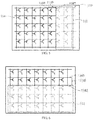
- FIG. 1 is a schematic structural diagram illustrating a display screen 100 according to an implementation of the disclosure.
- the display screen 100 includes a display layer 110 for image display.
- the display layer 110 has a fingerprint recognition area 111, and the fingerprint recognition area 111 is provided with an array of transparent thin film transistors 112 and transparent medium 113 among the transparent thin film transistors 112.
- each transparent thin film transistor 112 includes multiple electrode layers (1121, 1122, 1123) and an insulation layer 1124 among the multiple electrode layers (1121, 1122, 1123).
- the multiple electrode layers (1121, 1122, 1123) and the insulation layer 1124 are made from transparent materials.
- the multiple electrode layers (1121, 1122, 1123) are implemented as a gate electrode 1122, a drain electrode 1121, and a source electrode 1123.
- the gate electrode 1122, the drain electrode 1121, the source electrode 1123, and the transparent medium 113 are made from transparent materials, to increase light transmittance of the fingerprint recognition area 111.
- the multiple electrode layers (1121, 1122, 1123) are made from at least one material selected from a group consisting of Indium Tin Oxide (ITO) thin film, Aluminium-doped zinc oxide (ZnO:Al) thin film, and Gallium-doped zinc oxide (ZnO:Ga) thin film.
- ITO Indium Tin Oxide
- ZnO:Al Aluminium-doped zinc oxide
- ZnO:Ga Gallium-doped zinc oxide
- the fingerprint recognition area 111 is configured to allow lights transmitted or received by an optical fingerprint module to pass through, to increase light transmittance of the lights transmitted or received by the optical fingerprint module 202, thereby improving the accuracy of fingerprint recognition of the optical fingerprint module 202.
- the display layer 110 further has a peripheral area 114 adjacent to the fingerprint recognition area 111, and the peripheral area 114 is provided with an array of non-transparent thin film transistors 115.
- FIG. 3 is a cross-sectional view of the display screen 100 illustrated in FIG. 1 along line AA'. Since at least one electrode of the source electrode, the gate electrode, and the drain electrode of each non-transparent thin film transistor 115 is made from a metal such as Al, Mo, and Cu or an alloy thereof, the source electrode, the gate electrode, and/or the drain electrode of the non-transparent thin film transistor 115 do not allow light a to pass through. On the other hand, the gate electrode, the source electrode, and the drain electrode of each transparent thin film transistor 112 and the insulation layer 1124 among those electrodes are made from transparent materials and therefore, allow light a to pass through. As such, the light transmittance of the fingerprint recognition area 111 is larger than that of the peripheral area 114.
- the optical fingerprint module 202 when the optical fingerprint module 202 is on one side of the display screen 100 intended to away from a user, by providing the fingerprint recognition area 111 in the display screen 100, for the lights emitted from the optical fingerprint module 202 to the patterns of a finger, it is possible to reduce loss thereof in the display screen, thereby ensuring that more lights can be projected to and then reflected by the patterns of the finger; moreover, with the fingerprint recognition area 111, for lights reflected, the loss thereof in the display screen 100 can also be reduced, thereby ensuring that more lights can be projected onto the optical fingerprint module 202. The more the lights received by the optical fingerprint module 202, the higher the accuracy of the fingerprint recognition of the optical fingerprint module 202.
- the fingerprint recognition area 111 may correspond to a part of the display layer 110.
- the fingerprint recognition area 111 may correspond to the whole display layer 110, in this case, the fingerprint recognition area correspond to whole image display area of the display screen 100.
- the display layer 110 further includes multi-column scan lines (also known as gate lines) 1106, and the multi-column scan lines 1106 include at least one of transparent scan lines 1107 and non-transparent scan lines 1108 coupled with the transparent scan lines 1107.
- a column in the multi-column scan lines 1106 includes transparent scan lines 1107 and non-transparent scan lines 1108 coupled with the transparent scan lines, and a joint(s) 1109 between the transparent scan lines 1107 and the non-transparent scan lines 1108 are on the column of scan lines 1106.
- the multi-column scan lines 1106 include multi-column transparent scan lines 1107 and multi-column non-transparent scan lines 1108 parallel to the multi-column transparent scan lines 1107, and joints between one column of transparent scan lines 1107 and an adjacent column of non-transparent scan lines 1108 are on electrical connection lines 1110 between the column of transparent scan lines 1107 and the adjacent column of non-transparent scan lines 1108.
- the transparent scan lines 1107 are in the fingerprint recognition area 111, coupled with gates of the transparent thin film transistors 112, and configured to allow lights transmitted or received by the optical fingerprint module 202 to pass through, thereby increasing light transmittance of the display screen 100.
- the non-transparent scan lines 1108 are in the peripheral area 114 and coupled with gates of the non-transparent thin film transistors 115.
- the display layer 110 further includes multi-row data lines 1101.
- the extension direction of the multi-row data lines 1101 intersects the extension direction of the multi-column scan lines 1106.
- the multi-row data lines 1101 are perpendicular to the multi-column scan lines 1106.
- the multi-row data lines 1101 include at least one of transparent data lines 1102 and non-transparent data lines 1103 coupled with the transparent data lines 1102.
- the transparent data lines 1102 are in the fingerprint recognition area 111.
- the transparent data lines 1102 coupled with sources of the transparent thin film transistors 112.
- the transparent data lines 1102 are configured to allow lights transmitted or received by the optical fingerprint module 202 to pass through, thereby increasing light transmittance of the display screen 100.
- the non-transparent data lines 1103 are in the peripheral area 114 and coupled with sources of the non-transparent thin film transistors 115. Similar to the scan lines, a row in the multi-row data lines 1101 includes transparent data lines 1102 and non-transparent data lines 1103 coupled with the transparent data lines 1102, and a j oint(s) 1104 between the transparent data lines 1102 and the non-transparent data lines 1103 are on the row of data lines 1101. On the other hand, as illustrated in FIG.
- the multi-row data lines 1101 include multi-row transparent data lines 1102 and multi-row non-transparent data lines 1103 parallel to the multi-row transparent data lines 1102, and joints between one row of transparent data lines 1102 and an adjacent row of non-transparent data lines 1103 are on electrical connection lines 1105 between the row of transparent data lines 1102 and the adjacent row of non-transparent data lines 1103.
- the transparent scan lines 1107 and the non-transparent scan lines 1108 may have the same width and height.
- the transparent data lines 1102 and the non-transparent data lines 1103 may have the same width and height.
- the gate electrode, the source electrode, and the drain electrode of the transparent thin film transistors 112 and the gate electrode, the source electrode, and the drain electrode of the non-transparent thin film transistors 115 are not restricted in structure or size.
- the gate electrode, the source electrode, and the drain electrode of the transparent thin film transistors 112 may have the same or different structure or size as the gate electrode, the source electrode, and the drain electrode of the non-transparent thin film transistors 115, which may be determined according to actual display needs.
- the optical fingerprint module 202 corresponds to the fingerprint recognition area 111 in terms of position.
- the optical fingerprint module 202 is located directly below the fingerprint recognition area 111 (in a thickness direction of the display screen 100, and the optical fingerprint module 202 is on one side of the display screen 100 intended to away from the user).
- the size of the fingerprint recognition area 111 is larger than that of a light induction area of the optical fingerprint module 202.
- the fingerprint recognition area 111 may correspond to a part of the display layer 110.
- the fingerprint recognition area 111 may be in a central area of the display layer 110, or may be in an edge area of the display layer 110. In another implementation, the fingerprint recognition area 111 may correspond to the whole display layer 110. The following will be detailed in specific implementations.
- FIG. 4 is a schematic structural diagram illustrating a display screen 100 according to a first implementation of the disclosure.
- the fingerprint recognition area 111 corresponds to a part of the display layer 110.
- the fingerprint recognition area 111 is in a central area of the display layer 110, and is surrounded by the peripheral area 114. With such configuration. it is possible to adapt to a user's hand-held gesture, which facilitates the user to unlock with fingerprint, thereby improving user experience.
- the mobile terminal can be unlocked when the user simply put his or her thumb directly on the fingerprint recognition area 111 without moving the thumb.
- FIG. 5 to FIG. 7 are schematic structural diagrams illustrating a display screen 100 according to a second implementation of the disclosure.
- the fingerprint recognition area 111 may correspond to a part of the display layer 110 and may be in an edge area of the display layer 110.
- the peripheral area 114 is adjacent to the fingerprint recognition area 111.
- the transparent thin film transistors 112, the transparent scan lines 1107, and the transparent data lines 1102 can be disposed in the edge area of the display screen 100.
- joints between the transparent scan lines 1107 and the non-transparent scan lines 1108 may be reduced, and also fewer joints are needed between the transparent data lines 1102 and the non-transparent data lines 1103, such that the risk of poor contact between the transparent scan lines 1107 and the non-transparent scan lines 1108 can be reduced, and the risk of poor contact between the transparent data lines 1102 and the non-transparent data lines 1103 can be reduced.
- joints between one column of transparent scan lines 1107 and an adjacent column of non-transparent scan lines 1108 are located on electrical connection lines 1110 between the column of transparent scan lines 1107 and the adjacent column of non-transparent scan lines 1108. As illustrated in FIG.
- joints between one row of transparent data lines 1102 and an adjacent row of non-transparent data lines 1103 are located on electrical connection lines 1105 between the row of transparent data lines 1102 and the adjacent row of non-transparent data lines 1103.
- the joints between the column of transparent scan lines 1107 and the adjacent column of non-transparent scan lines 1108 is reduced, and the joints between the row of transparent data lines 1102 and the adjacent row of non-transparent data lines 1103 is also reduced.
- FIG. 8 is a schematic structural diagram illustrating a display screen 100 according to a third implementation of the disclosure.
- the fingerprint recognition area 111 corresponds to the whole display layer 110.
- fingerprint recognition can be implemented in any area of the display layer 110, thereby improving the user experience.
- the fingerprint recognition area 111 may be embodied as multiple fingerprint recognition areas.
- the multiple fingerprint recognition areas 111 are distributed in an area corresponding to the whole display layer 110. With such structural design, it is possible to reduce a risk of inaccuracy and/or failure of recognition due to existence of foreign materials in one or more of fingerprint recognition area 111 of the display screen 100.
- the fingerprint recognition can be implemented in any area of the display layer 110, thereby improving the user experience.
- the fingerprint recognition area 111 can be circular, square, elliptical, irregular shape or the like.
- each transparent thin film transistor 112 includes the transparent source electrode 1121, the transparent gate electrode 1122, and the transparent drain electrode 1123, where the transparent source electrode 1121, the transparent gate electrode 1122, and the transparent drain electrode 1123 may be made from at least one material selected from a group consisting of ITO thin film, ZnO:Al thin film, and ZnO:Ga thin film or made from other transparent materials.
- the transparent medium 113 is disposed among the transparent thin film transistors 112.
- the transparent medium 113 is made from at least one material selected from a group consisting of Silicon dioxide (SiO2) thin film and Aluminum oxide (Al 2 O 3 ) thin film or made from other transparent materials.
- an insulation layer 1124 is disposed among the transparent source electrode 1121, the transparent gate electrode 1122, and the transparent drain electrode 1123.
- the insulation layer 1124 is made from SiO2 thin film, Al2O3 thin film, or other transparent insulation materials.
- the transparent gate electrode 1122 can be formed on a transparent substrate 1125 through a magnetron sputtering deposition and etching process, and then the transparent insulation layer 1124, the transparent source electrode 1121, and the transparent drain electrode 1123 can be formed on the transparent gate electrode 1122.
- the transparent scan lines 1107 are made from at least one material selected from a group consisting of ITO thin film, ZnO:Al thin film, and ZnO:Ga thin film.
- the transparent data lines 1102 are made from at least one material selected from a group consisting of ITO thin film, ZnO:Al thin film, and ZnO:Ga thin film.
- the transparent scan lines 1107 and the transparent data lines 1102 may be formed through a magnetron sputtering deposition and etching process.
- the joints between the transparent scan lines 1107 and the non-transparent scan lines 1108 and the joints between the transparent data lines 1102 and the non-transparent data lines 1103 can be made from a transitional material.
- the joints between the transparent scan lines 1107 and non-transparent scan lines 1108 may be made from a mixture of the ITO thin film and the Al metal.
- the display screen 100 further includes a light-shielding layer 117.
- the light-shielding layer 117 is disposed on one side of the display layer 110 intended to away from a user and defines a through hole 118.
- the through hole 118 is located in a position corresponding to the fingerprint recognition area 111, whereby the optical fingerprint module 202 can transmit and receive lights through the fingerprint recognition area 111 and the through hole 118.
- the through hole 118 has a shape and size same as the fingerprint recognition area 111.
- the display screen 100 may be an organic light-emitting diode (OLED) display.
- the display layer 110 is a luminescent layer.
- the light-shielding layer 117 is a foam layer.
- the foam layer is configured to block lights from passing through the display layer 110, to hide internal structures disposed under the display layer 110, and to exhibit a color of the light-shielding layer 117 when the display layer 110 emit lights (that is, in a screen-off state).
- the light-shielding layer 117 can be black, white, or other opaque colors. By defining the through hole 118 on the foam layer, lights may be allowed to pass through the light-shielding layer 117.
- FIG. 11 is a schematic structural diagram illustrating a display device 200 according to an implementation of the disclosure.
- the display device 200 includes the display screen 100 according to any of the implementations described above.
- the display device 200 further includes an optical fingerprint module 202 and a frame 201.
- the display screen 100 and the optical fingerprint module 202 are fixed on the frame 201, the optical fingerprint module 202 is located on one side of the display screen 100 intended to away from a user, the optical fingerprint module 202 is located in a position corresponding to the fingerprint recognition area 111, to allow lights transmitted and received pass through the fingerprint recognition area 111.
- the optical fingerprint module 202 includes a light emitter 203 and a light inductor 204, the light emitter 203 is configured to emit induced light b and the light inductor 204 is configured to receive induced light c.
- the finger is in contact with a surface of the display screen 100, lights emitted by the light emitter 203 form an incident light b and the incident light b is projected onto patterns 205 of a finger after sequentially passing through the through hole 118 and the fingerprint recognition area 111 of the display layer 110.
- the display layer 110 has the fingerprint recognition area 111, and the fingerprint recognition area 111 is provided with the transparent thin film transistors 112, the transparent medium 113 among the transparent thin film transistors 112, the transparent scan lines 1107, and the transparent data lines 1102, the light transmittance in the display layer 110 of the induced light b can be increased, thereby making the intensity of the incident light b projected onto the patterns 205 higher. As such, the intensity of reflected lights c formed from incident lights b reflected by the patterns 205 of the finger can also be increased.
- transmittance of the induced light c in the fingerprint recognition area 111 of the display layer 110 can also be increased, and intensity of the induced light c received by light inductor 204 may be increased, thereby improving accuracy of recognition of the optical fingerprint module 202.
- FIG. 12 is a schematic structural diagram illustrating a mobile terminal 300 according to an implementation of the disclosure.
- the mobile terminal 300 includes the display device 200.
- the display device 200 includes a display screen 100 and an optical fingerprint module 202 disposed on one side of the display screen 100 intended to away from a user.
- the display screen 100 has a fingerprint recognition area 111. Since the fingerprint recognition area 111 is provided with the array of transparent thin film transistors 112 and transparent medium 113 among the transparent thin film transistors 112, light transmittance of the fingerprint recognition area 111 can be increased.
- the optical fingerprint module 202 is located in a position corresponding to the fingerprint recognition area 111, such that the intensity of the lights emitted from the optical fingerprint module 202 to the patterns 205 may be increased, and accordingly the intensity of the induced light reflected by the patterns 205 may be increased, thereby improving the accuracy of fingerprint recognition of the optical fingerprint module 202.
Landscapes
- Engineering & Computer Science (AREA)
- Physics & Mathematics (AREA)
- General Physics & Mathematics (AREA)
- Theoretical Computer Science (AREA)
- Multimedia (AREA)
- Human Computer Interaction (AREA)
- Computer Hardware Design (AREA)
- Health & Medical Sciences (AREA)
- General Health & Medical Sciences (AREA)
- Vascular Medicine (AREA)
- Microelectronics & Electronic Packaging (AREA)
- Devices For Indicating Variable Information By Combining Individual Elements (AREA)
- Image Input (AREA)
- Collating Specific Patterns (AREA)
Applications Claiming Priority (2)
| Application Number | Priority Date | Filing Date | Title |
|---|---|---|---|
| CN201710289263.2A CN107195675B (zh) | 2017-04-27 | 2017-04-27 | 显示屏、显示装置及移动终端 |
| PCT/CN2018/083042 WO2018196636A1 (zh) | 2017-04-27 | 2018-04-13 | 显示屏、显示装置及移动终端 |
Publications (3)
| Publication Number | Publication Date |
|---|---|
| EP3584842A1 true EP3584842A1 (de) | 2019-12-25 |
| EP3584842A4 EP3584842A4 (de) | 2020-03-04 |
| EP3584842B1 EP3584842B1 (de) | 2023-09-20 |
Family
ID=59873596
Family Applications (1)
| Application Number | Title | Priority Date | Filing Date |
|---|---|---|---|
| EP18790395.0A Active EP3584842B1 (de) | 2017-04-27 | 2018-04-13 | Anzeigebildschirm, anzeigevorrichtung und mobiles endgerät |
Country Status (4)
| Country | Link |
|---|---|
| US (1) | US11183531B2 (de) |
| EP (1) | EP3584842B1 (de) |
| CN (2) | CN110610990B (de) |
| WO (1) | WO2018196636A1 (de) |
Cited By (1)
| Publication number | Priority date | Publication date | Assignee | Title |
|---|---|---|---|---|
| EP3647995A4 (de) * | 2018-09-21 | 2020-05-06 | Shenzhen Goodix Technology Co., Ltd. | Elektronische vorrichtung für fingerabdruckidentifikation |
Families Citing this family (27)
| Publication number | Priority date | Publication date | Assignee | Title |
|---|---|---|---|---|
| CN110610990B (zh) * | 2017-04-27 | 2023-06-02 | Oppo广东移动通信有限公司 | 显示屏、显示装置及移动终端 |
| CN107863370A (zh) * | 2017-09-30 | 2018-03-30 | 昆山国显光电有限公司 | 显示装置 |
| CN107608122B (zh) * | 2017-10-19 | 2021-01-15 | Oppo广东移动通信有限公司 | 显示屏、功能组件及移动终端 |
| CN109697396A (zh) * | 2017-10-24 | 2019-04-30 | 华为终端(东莞)有限公司 | 一种有机电致发光显示面板、显示模组及电子设备 |
| CN109711229B (zh) * | 2017-10-26 | 2021-12-21 | 中芯国际集成电路制造(上海)有限公司 | 一种指纹识别芯片及其制造方法和电子装置 |
| CN110033699A (zh) * | 2018-01-12 | 2019-07-19 | 京东方科技集团股份有限公司 | 显示基板及其制作方法、显示装置 |
| JP2019144724A (ja) * | 2018-02-19 | 2019-08-29 | 京セラ株式会社 | 電子機器及び制御方法 |
| CN108615746A (zh) * | 2018-04-28 | 2018-10-02 | 武汉天马微电子有限公司 | 显示面板和显示装置 |
| CN108711378B (zh) * | 2018-04-28 | 2021-01-05 | 厦门天马微电子有限公司 | 显示面板和显示装置 |
| CN109063621A (zh) * | 2018-07-25 | 2018-12-21 | 维沃移动通信有限公司 | 一种移动终端 |
| US11397452B2 (en) * | 2018-07-31 | 2022-07-26 | Hewlett-Packard Development Company, L.P. | Displays with partial transparent areas |
| CN108898955A (zh) * | 2018-07-31 | 2018-11-27 | 武汉天马微电子有限公司 | 一种显示面板及显示装置 |
| CN109031823B (zh) * | 2018-07-31 | 2023-06-30 | Oppo广东移动通信有限公司 | 显示屏、电子设备及其控制方法 |
| CN109660645A (zh) * | 2018-12-18 | 2019-04-19 | 武汉华星光电半导体显示技术有限公司 | 一种显示装置及其使用方法 |
| CN109817665A (zh) * | 2019-01-09 | 2019-05-28 | 昆山国显光电有限公司 | 像素结构和显示面板 |
| CN110060651A (zh) * | 2019-06-06 | 2019-07-26 | 合肥京东方光电科技有限公司 | 一种显示面板、显示装置及其驱动方法 |
| US11694613B2 (en) * | 2019-07-25 | 2023-07-04 | Hewlett-Packard Development Company, L.P. | Displays with partial transparent areas |
| WO2021087742A1 (zh) * | 2019-11-05 | 2021-05-14 | 深圳市汇顶科技股份有限公司 | 屏下指纹识别装置、lcd指纹识别系统和电子设备 |
| KR102865946B1 (ko) * | 2019-12-24 | 2025-09-26 | 엘지디스플레이 주식회사 | 유기발광 표시장치 |
| US11653534B2 (en) * | 2020-03-05 | 2023-05-16 | Samsung Display Co., Ltd. | Display device and electronic apparatus |
| CN111524451B (zh) | 2020-04-30 | 2022-03-22 | 昆山国显光电有限公司 | 显示面板及显示装置 |
| KR102782859B1 (ko) * | 2020-06-02 | 2025-03-17 | 삼성디스플레이 주식회사 | 표시 장치 |
| CN111881719B (zh) * | 2020-06-09 | 2024-04-16 | 青岛奥美克生物信息科技有限公司 | 非接触式生物识别引导装置、方法以及生物特征识别系统 |
| CN112038368A (zh) * | 2020-08-17 | 2020-12-04 | 武汉华星光电半导体显示技术有限公司 | 阵列基板及oled显示面板 |
| KR102682607B1 (ko) * | 2020-10-19 | 2024-07-09 | 엘지디스플레이 주식회사 | 표시패널과 이를 이용한 표시장치 |
| CN113299855B (zh) * | 2021-05-21 | 2023-09-22 | 京东方科技集团股份有限公司 | 显示装置、显示面板及其制造方法 |
| WO2024062570A1 (ja) * | 2022-09-21 | 2024-03-28 | シャープディスプレイテクノロジー株式会社 | 表示装置 |
Family Cites Families (19)
| Publication number | Priority date | Publication date | Assignee | Title |
|---|---|---|---|---|
| KR100873497B1 (ko) * | 2002-10-17 | 2008-12-15 | 삼성전자주식회사 | 지문 인식 소자를 내장한 일체형 액정표시장치 및 이의제조 방법 |
| CN100530607C (zh) | 2007-12-11 | 2009-08-19 | 西安交通大学 | 一种ZnO基透明薄膜晶体管阵列的制备方法 |
| US20140292666A1 (en) * | 2013-03-26 | 2014-10-02 | Mobile Identity Management and Biometrics consortium | Method and Apparatuses of User Interaction Control with Touch Display Device Integrated with Fingerprint Imager |
| US20130287274A1 (en) * | 2012-04-29 | 2013-10-31 | Weidong Shi | Methods and Apparatuses of Unified Capacitive Based Sensing of Touch and Fingerprint |
| US8994690B2 (en) * | 2012-04-29 | 2015-03-31 | Weidong Shi | Method and apparatuses of transparent fingerprint imager integrated with touch display device |
| TWI486844B (zh) * | 2012-09-25 | 2015-06-01 | Au Optronics Corp | 光學觸控掃描裝置 |
| US20150109214A1 (en) * | 2013-10-22 | 2015-04-23 | Weidong Shi | Methods and Apparatuses of touch-fingerprinting Display |
| CN104252277A (zh) * | 2014-09-18 | 2014-12-31 | 叶志 | 一种触摸面板阵列以及用于触摸面板阵列的扫描方法 |
| TWI559185B (zh) * | 2014-10-03 | 2016-11-21 | 速博思股份有限公司 | 兼具指紋辨識與觸控偵測的顯示裝置 |
| US9679182B2 (en) * | 2014-11-12 | 2017-06-13 | Crucialtec Co., Ltd. | Display apparatus capable of image scanning and driving method thereof |
| KR20160088764A (ko) * | 2015-01-16 | 2016-07-26 | 삼성전자주식회사 | 플렉서블 디바이스 및 그 동작 방법 |
| CN104850292B (zh) * | 2015-06-01 | 2017-09-29 | 京东方科技集团股份有限公司 | 一种内嵌式触摸屏、其驱动方法及显示装置 |
| US10276593B2 (en) * | 2015-06-05 | 2019-04-30 | Sharp Kabushiki Kaisha | Active matrix substrate and method for manufacturing same, display device using active matrix substrate |
| US10268884B2 (en) * | 2016-01-29 | 2019-04-23 | Synaptics Incorporated | Optical fingerprint sensor under a display |
| CN108268852A (zh) * | 2016-03-17 | 2018-07-10 | 广东欧珀移动通信有限公司 | 屏幕组件、指纹采集和识别方法、移动终端及电子设备 |
| CN105702176B (zh) * | 2016-04-12 | 2018-06-15 | 深圳市华星光电技术有限公司 | 具有指纹识别的显示面板及显示装置 |
| CN106022276B (zh) * | 2016-05-25 | 2019-06-07 | 京东方科技集团股份有限公司 | 指纹识别器件及其制作方法、显示器件、显示装置 |
| CN107451513B (zh) * | 2016-05-31 | 2023-12-29 | 宸鸿科技(厦门)有限公司 | 指纹辨识装置 |
| CN110610990B (zh) * | 2017-04-27 | 2023-06-02 | Oppo广东移动通信有限公司 | 显示屏、显示装置及移动终端 |
-
2017
- 2017-04-27 CN CN201910829418.6A patent/CN110610990B/zh active Active
- 2017-04-27 CN CN201710289263.2A patent/CN107195675B/zh active Active
-
2018
- 2018-04-13 WO PCT/CN2018/083042 patent/WO2018196636A1/zh not_active Ceased
- 2018-04-13 EP EP18790395.0A patent/EP3584842B1/de active Active
-
2019
- 2019-09-26 US US16/584,207 patent/US11183531B2/en active Active
Cited By (1)
| Publication number | Priority date | Publication date | Assignee | Title |
|---|---|---|---|---|
| EP3647995A4 (de) * | 2018-09-21 | 2020-05-06 | Shenzhen Goodix Technology Co., Ltd. | Elektronische vorrichtung für fingerabdruckidentifikation |
Also Published As
| Publication number | Publication date |
|---|---|
| EP3584842B1 (de) | 2023-09-20 |
| CN107195675B (zh) | 2019-09-27 |
| EP3584842A4 (de) | 2020-03-04 |
| US20200020737A1 (en) | 2020-01-16 |
| CN110610990B (zh) | 2023-06-02 |
| CN107195675A (zh) | 2017-09-22 |
| WO2018196636A1 (zh) | 2018-11-01 |
| US11183531B2 (en) | 2021-11-23 |
| CN110610990A (zh) | 2019-12-24 |
Similar Documents
| Publication | Publication Date | Title |
|---|---|---|
| US11183531B2 (en) | Display screen, display module, and terminal | |
| EP3588367B1 (de) | Anzeigebildschirm, anzeigevorrichtung und mobiles endgerät | |
| KR102508724B1 (ko) | 지문 센싱 유닛 및 이를 포함하는 표시 장치 | |
| US11538270B2 (en) | Display panel and display device | |
| US11644914B2 (en) | Display panel and display device | |
| KR20220133844A (ko) | 표시 장치 | |
| US11681395B2 (en) | Display substrate, display device and detection method by using display device | |
| US12310135B2 (en) | Line recognition module, fabricating method thereof and display device | |
| US10713999B2 (en) | OLED display panel, driving method thereof and display device | |
| USRE50651E1 (en) | Electro-luminescence display apparatus | |
| WO2020196788A1 (ja) | 検出装置付き表示機器 | |
| US11481071B2 (en) | Touch display panel | |
| US20210192171A1 (en) | Fingerprint identification assembly, display substrate, display panel and fingerprint identification method | |
| KR102837613B1 (ko) | 표시 장치 및 이의 제조 방법 | |
| TWI724672B (zh) | 具有光學掃描功能的觸控板 | |
| KR20230103247A (ko) | 표시 장치 | |
| TWI798724B (zh) | 具高穿透率顯示模組的電子裝置 | |
| CN107340903B (zh) | 触控显示设备 | |
| KR20210080953A (ko) | 터치 디스플레이 장치 및 디스플레이 패널 | |
| WO2026044758A1 (zh) | 显示面板及显示装置 | |
| WO2026091920A1 (zh) | 显示面板及显示装置 | |
| CN114730503A (zh) | 屏下指纹识别模组、显示组件及显示装置 | |
| CN117957595A (zh) | 显示面板、显示面板的制造方法以及显示装置 | |
| CN117542091A (zh) | 光学指纹感测装置 | |
| CN117769328A (zh) | 显示装置和制造显示装置的方法 |
Legal Events
| Date | Code | Title | Description |
|---|---|---|---|
| STAA | Information on the status of an ep patent application or granted ep patent |
Free format text: STATUS: THE INTERNATIONAL PUBLICATION HAS BEEN MADE |
|
| PUAI | Public reference made under article 153(3) epc to a published international application that has entered the european phase |
Free format text: ORIGINAL CODE: 0009012 |
|
| STAA | Information on the status of an ep patent application or granted ep patent |
Free format text: STATUS: REQUEST FOR EXAMINATION WAS MADE |
|
| 17P | Request for examination filed |
Effective date: 20190920 |
|
| AK | Designated contracting states |
Kind code of ref document: A1 Designated state(s): AL AT BE BG CH CY CZ DE DK EE ES FI FR GB GR HR HU IE IS IT LI LT LU LV MC MK MT NL NO PL PT RO RS SE SI SK SM TR |
|
| AX | Request for extension of the european patent |
Extension state: BA ME |
|
| A4 | Supplementary search report drawn up and despatched |
Effective date: 20200203 |
|
| RIC1 | Information provided on ipc code assigned before grant |
Ipc: G06K 9/00 20060101ALI20200128BHEP Ipc: H01L 23/50 20060101ALI20200128BHEP Ipc: G06K 9/20 20060101ALI20200128BHEP Ipc: H01L 29/43 20060101AFI20200128BHEP Ipc: G06K 9/22 20060101ALI20200128BHEP Ipc: H01L 29/786 20060101ALI20200128BHEP Ipc: H01L 23/29 20060101ALI20200128BHEP |
|
| DAV | Request for validation of the european patent (deleted) | ||
| DAX | Request for extension of the european patent (deleted) | ||
| STAA | Information on the status of an ep patent application or granted ep patent |
Free format text: STATUS: EXAMINATION IS IN PROGRESS |
|
| 17Q | First examination report despatched |
Effective date: 20210407 |
|
| REG | Reference to a national code |
Ref country code: DE Ref legal event code: R079 Free format text: PREVIOUS MAIN CLASS: H01L0029430000 Ipc: G09G0003322500 Ref country code: DE Ref legal event code: R079 Ref document number: 602018057959 Country of ref document: DE Free format text: PREVIOUS MAIN CLASS: H01L0029430000 Ipc: G09G0003322500 |
|
| GRAP | Despatch of communication of intention to grant a patent |
Free format text: ORIGINAL CODE: EPIDOSNIGR1 |
|
| STAA | Information on the status of an ep patent application or granted ep patent |
Free format text: STATUS: GRANT OF PATENT IS INTENDED |
|
| INTG | Intention to grant announced |
Effective date: 20230629 |
|
| RIC1 | Information provided on ipc code assigned before grant |
Ipc: H01L 29/786 20060101ALI20230616BHEP Ipc: H01L 29/43 20060101ALI20230616BHEP Ipc: H01L 23/50 20060101ALI20230616BHEP Ipc: H01L 23/29 20060101ALI20230616BHEP Ipc: G06V 40/13 20220101ALI20230616BHEP Ipc: G06V 10/147 20220101ALI20230616BHEP Ipc: G09G 3/3225 20160101AFI20230616BHEP |
|
| GRAS | Grant fee paid |
Free format text: ORIGINAL CODE: EPIDOSNIGR3 |
|
| GRAA | (expected) grant |
Free format text: ORIGINAL CODE: 0009210 |
|
| STAA | Information on the status of an ep patent application or granted ep patent |
Free format text: STATUS: THE PATENT HAS BEEN GRANTED |
|
| AK | Designated contracting states |
Kind code of ref document: B1 Designated state(s): AL AT BE BG CH CY CZ DE DK EE ES FI FR GB GR HR HU IE IS IT LI LT LU LV MC MK MT NL NO PL PT RO RS SE SI SK SM TR |
|
| REG | Reference to a national code |
Ref country code: GB Ref legal event code: FG4D |
|
| REG | Reference to a national code |
Ref country code: CH Ref legal event code: EP |
|
| REG | Reference to a national code |
Ref country code: DE Ref legal event code: R096 Ref document number: 602018057959 Country of ref document: DE |
|
| REG | Reference to a national code |
Ref country code: IE Ref legal event code: FG4D |
|
| P01 | Opt-out of the competence of the unified patent court (upc) registered |
Effective date: 20231016 |
|
| REG | Reference to a national code |
Ref country code: LT Ref legal event code: MG9D |
|
| PG25 | Lapsed in a contracting state [announced via postgrant information from national office to epo] |
Ref country code: GR Free format text: LAPSE BECAUSE OF FAILURE TO SUBMIT A TRANSLATION OF THE DESCRIPTION OR TO PAY THE FEE WITHIN THE PRESCRIBED TIME-LIMIT Effective date: 20231221 |
|
| REG | Reference to a national code |
Ref country code: NL Ref legal event code: MP Effective date: 20230920 |
|
| PG25 | Lapsed in a contracting state [announced via postgrant information from national office to epo] |
Ref country code: SE Free format text: LAPSE BECAUSE OF FAILURE TO SUBMIT A TRANSLATION OF THE DESCRIPTION OR TO PAY THE FEE WITHIN THE PRESCRIBED TIME-LIMIT Effective date: 20230920 Ref country code: RS Free format text: LAPSE BECAUSE OF FAILURE TO SUBMIT A TRANSLATION OF THE DESCRIPTION OR TO PAY THE FEE WITHIN THE PRESCRIBED TIME-LIMIT Effective date: 20230920 Ref country code: NO Free format text: LAPSE BECAUSE OF FAILURE TO SUBMIT A TRANSLATION OF THE DESCRIPTION OR TO PAY THE FEE WITHIN THE PRESCRIBED TIME-LIMIT Effective date: 20231220 Ref country code: LV Free format text: LAPSE BECAUSE OF FAILURE TO SUBMIT A TRANSLATION OF THE DESCRIPTION OR TO PAY THE FEE WITHIN THE PRESCRIBED TIME-LIMIT Effective date: 20230920 Ref country code: LT Free format text: LAPSE BECAUSE OF FAILURE TO SUBMIT A TRANSLATION OF THE DESCRIPTION OR TO PAY THE FEE WITHIN THE PRESCRIBED TIME-LIMIT Effective date: 20230920 Ref country code: HR Free format text: LAPSE BECAUSE OF FAILURE TO SUBMIT A TRANSLATION OF THE DESCRIPTION OR TO PAY THE FEE WITHIN THE PRESCRIBED TIME-LIMIT Effective date: 20230920 Ref country code: GR Free format text: LAPSE BECAUSE OF FAILURE TO SUBMIT A TRANSLATION OF THE DESCRIPTION OR TO PAY THE FEE WITHIN THE PRESCRIBED TIME-LIMIT Effective date: 20231221 Ref country code: FI Free format text: LAPSE BECAUSE OF FAILURE TO SUBMIT A TRANSLATION OF THE DESCRIPTION OR TO PAY THE FEE WITHIN THE PRESCRIBED TIME-LIMIT Effective date: 20230920 |
|
| REG | Reference to a national code |
Ref country code: AT Ref legal event code: MK05 Ref document number: 1614042 Country of ref document: AT Kind code of ref document: T Effective date: 20230920 |
|
| PG25 | Lapsed in a contracting state [announced via postgrant information from national office to epo] |
Ref country code: NL Free format text: LAPSE BECAUSE OF FAILURE TO SUBMIT A TRANSLATION OF THE DESCRIPTION OR TO PAY THE FEE WITHIN THE PRESCRIBED TIME-LIMIT Effective date: 20230920 |
|
| PG25 | Lapsed in a contracting state [announced via postgrant information from national office to epo] |
Ref country code: IS Free format text: LAPSE BECAUSE OF FAILURE TO SUBMIT A TRANSLATION OF THE DESCRIPTION OR TO PAY THE FEE WITHIN THE PRESCRIBED TIME-LIMIT Effective date: 20240120 |
|
| PG25 | Lapsed in a contracting state [announced via postgrant information from national office to epo] |
Ref country code: AT Free format text: LAPSE BECAUSE OF FAILURE TO SUBMIT A TRANSLATION OF THE DESCRIPTION OR TO PAY THE FEE WITHIN THE PRESCRIBED TIME-LIMIT Effective date: 20230920 |
|
| PG25 | Lapsed in a contracting state [announced via postgrant information from national office to epo] |
Ref country code: ES Free format text: LAPSE BECAUSE OF FAILURE TO SUBMIT A TRANSLATION OF THE DESCRIPTION OR TO PAY THE FEE WITHIN THE PRESCRIBED TIME-LIMIT Effective date: 20230920 |
|
| PG25 | Lapsed in a contracting state [announced via postgrant information from national office to epo] |
Ref country code: SM Free format text: LAPSE BECAUSE OF FAILURE TO SUBMIT A TRANSLATION OF THE DESCRIPTION OR TO PAY THE FEE WITHIN THE PRESCRIBED TIME-LIMIT Effective date: 20230920 Ref country code: RO Free format text: LAPSE BECAUSE OF FAILURE TO SUBMIT A TRANSLATION OF THE DESCRIPTION OR TO PAY THE FEE WITHIN THE PRESCRIBED TIME-LIMIT Effective date: 20230920 Ref country code: IS Free format text: LAPSE BECAUSE OF FAILURE TO SUBMIT A TRANSLATION OF THE DESCRIPTION OR TO PAY THE FEE WITHIN THE PRESCRIBED TIME-LIMIT Effective date: 20240120 Ref country code: ES Free format text: LAPSE BECAUSE OF FAILURE TO SUBMIT A TRANSLATION OF THE DESCRIPTION OR TO PAY THE FEE WITHIN THE PRESCRIBED TIME-LIMIT Effective date: 20230920 Ref country code: EE Free format text: LAPSE BECAUSE OF FAILURE TO SUBMIT A TRANSLATION OF THE DESCRIPTION OR TO PAY THE FEE WITHIN THE PRESCRIBED TIME-LIMIT Effective date: 20230920 Ref country code: CZ Free format text: LAPSE BECAUSE OF FAILURE TO SUBMIT A TRANSLATION OF THE DESCRIPTION OR TO PAY THE FEE WITHIN THE PRESCRIBED TIME-LIMIT Effective date: 20230920 Ref country code: AT Free format text: LAPSE BECAUSE OF FAILURE TO SUBMIT A TRANSLATION OF THE DESCRIPTION OR TO PAY THE FEE WITHIN THE PRESCRIBED TIME-LIMIT Effective date: 20230920 Ref country code: PT Free format text: LAPSE BECAUSE OF FAILURE TO SUBMIT A TRANSLATION OF THE DESCRIPTION OR TO PAY THE FEE WITHIN THE PRESCRIBED TIME-LIMIT Effective date: 20240122 Ref country code: SK Free format text: LAPSE BECAUSE OF FAILURE TO SUBMIT A TRANSLATION OF THE DESCRIPTION OR TO PAY THE FEE WITHIN THE PRESCRIBED TIME-LIMIT Effective date: 20230920 |
|
| PG25 | Lapsed in a contracting state [announced via postgrant information from national office to epo] |
Ref country code: PL Free format text: LAPSE BECAUSE OF FAILURE TO SUBMIT A TRANSLATION OF THE DESCRIPTION OR TO PAY THE FEE WITHIN THE PRESCRIBED TIME-LIMIT Effective date: 20230920 Ref country code: IT Free format text: LAPSE BECAUSE OF FAILURE TO SUBMIT A TRANSLATION OF THE DESCRIPTION OR TO PAY THE FEE WITHIN THE PRESCRIBED TIME-LIMIT Effective date: 20230920 |
|
| REG | Reference to a national code |
Ref country code: DE Ref legal event code: R097 Ref document number: 602018057959 Country of ref document: DE |
|
| PG25 | Lapsed in a contracting state [announced via postgrant information from national office to epo] |
Ref country code: DK Free format text: LAPSE BECAUSE OF FAILURE TO SUBMIT A TRANSLATION OF THE DESCRIPTION OR TO PAY THE FEE WITHIN THE PRESCRIBED TIME-LIMIT Effective date: 20230920 |
|
| PLBE | No opposition filed within time limit |
Free format text: ORIGINAL CODE: 0009261 |
|
| STAA | Information on the status of an ep patent application or granted ep patent |
Free format text: STATUS: NO OPPOSITION FILED WITHIN TIME LIMIT |
|
| PG25 | Lapsed in a contracting state [announced via postgrant information from national office to epo] |
Ref country code: DK Free format text: LAPSE BECAUSE OF FAILURE TO SUBMIT A TRANSLATION OF THE DESCRIPTION OR TO PAY THE FEE WITHIN THE PRESCRIBED TIME-LIMIT Effective date: 20230920 |
|
| 26N | No opposition filed |
Effective date: 20240621 |
|
| PG25 | Lapsed in a contracting state [announced via postgrant information from national office to epo] |
Ref country code: SI Free format text: LAPSE BECAUSE OF FAILURE TO SUBMIT A TRANSLATION OF THE DESCRIPTION OR TO PAY THE FEE WITHIN THE PRESCRIBED TIME-LIMIT Effective date: 20230920 |
|
| PG25 | Lapsed in a contracting state [announced via postgrant information from national office to epo] |
Ref country code: SI Free format text: LAPSE BECAUSE OF FAILURE TO SUBMIT A TRANSLATION OF THE DESCRIPTION OR TO PAY THE FEE WITHIN THE PRESCRIBED TIME-LIMIT Effective date: 20230920 |
|
| REG | Reference to a national code |
Ref country code: DE Ref legal event code: R119 Ref document number: 602018057959 Country of ref document: DE |
|
| PG25 | Lapsed in a contracting state [announced via postgrant information from national office to epo] |
Ref country code: BG Free format text: LAPSE BECAUSE OF FAILURE TO SUBMIT A TRANSLATION OF THE DESCRIPTION OR TO PAY THE FEE WITHIN THE PRESCRIBED TIME-LIMIT Effective date: 20230920 |
|
| PG25 | Lapsed in a contracting state [announced via postgrant information from national office to epo] |
Ref country code: MC Free format text: LAPSE BECAUSE OF FAILURE TO SUBMIT A TRANSLATION OF THE DESCRIPTION OR TO PAY THE FEE WITHIN THE PRESCRIBED TIME-LIMIT Effective date: 20230920 |
|
| PG25 | Lapsed in a contracting state [announced via postgrant information from national office to epo] |
Ref country code: MC Free format text: LAPSE BECAUSE OF FAILURE TO SUBMIT A TRANSLATION OF THE DESCRIPTION OR TO PAY THE FEE WITHIN THE PRESCRIBED TIME-LIMIT Effective date: 20230920 Ref country code: BG Free format text: LAPSE BECAUSE OF FAILURE TO SUBMIT A TRANSLATION OF THE DESCRIPTION OR TO PAY THE FEE WITHIN THE PRESCRIBED TIME-LIMIT Effective date: 20230920 |
|
| REG | Reference to a national code |
Ref country code: CH Ref legal event code: PL |
|
| PG25 | Lapsed in a contracting state [announced via postgrant information from national office to epo] |
Ref country code: LU Free format text: LAPSE BECAUSE OF NON-PAYMENT OF DUE FEES Effective date: 20240413 |
|
| REG | Reference to a national code |
Ref country code: BE Ref legal event code: MM Effective date: 20240430 |
|
| PG25 | Lapsed in a contracting state [announced via postgrant information from national office to epo] |
Ref country code: LU Free format text: LAPSE BECAUSE OF NON-PAYMENT OF DUE FEES Effective date: 20240413 |
|
| PG25 | Lapsed in a contracting state [announced via postgrant information from national office to epo] |
Ref country code: DE Free format text: LAPSE BECAUSE OF NON-PAYMENT OF DUE FEES Effective date: 20241105 |
|
| PG25 | Lapsed in a contracting state [announced via postgrant information from national office to epo] |
Ref country code: BE Free format text: LAPSE BECAUSE OF NON-PAYMENT OF DUE FEES Effective date: 20240430 |
|
| PG25 | Lapsed in a contracting state [announced via postgrant information from national office to epo] |
Ref country code: FR Free format text: LAPSE BECAUSE OF NON-PAYMENT OF DUE FEES Effective date: 20240430 |
|
| PG25 | Lapsed in a contracting state [announced via postgrant information from national office to epo] |
Ref country code: FR Free format text: LAPSE BECAUSE OF NON-PAYMENT OF DUE FEES Effective date: 20240430 Ref country code: DE Free format text: LAPSE BECAUSE OF NON-PAYMENT OF DUE FEES Effective date: 20241105 Ref country code: BE Free format text: LAPSE BECAUSE OF NON-PAYMENT OF DUE FEES Effective date: 20240430 Ref country code: CH Free format text: LAPSE BECAUSE OF NON-PAYMENT OF DUE FEES Effective date: 20240430 |
|
| PG25 | Lapsed in a contracting state [announced via postgrant information from national office to epo] |
Ref country code: IE Free format text: LAPSE BECAUSE OF NON-PAYMENT OF DUE FEES Effective date: 20240413 |
|
| PG25 | Lapsed in a contracting state [announced via postgrant information from national office to epo] |
Ref country code: CY Free format text: LAPSE BECAUSE OF FAILURE TO SUBMIT A TRANSLATION OF THE DESCRIPTION OR TO PAY THE FEE WITHIN THE PRESCRIBED TIME-LIMIT; INVALID AB INITIO Effective date: 20180413 |
|
| PG25 | Lapsed in a contracting state [announced via postgrant information from national office to epo] |
Ref country code: HU Free format text: LAPSE BECAUSE OF FAILURE TO SUBMIT A TRANSLATION OF THE DESCRIPTION OR TO PAY THE FEE WITHIN THE PRESCRIBED TIME-LIMIT; INVALID AB INITIO Effective date: 20180413 |
|
| PGFP | Annual fee paid to national office [announced via postgrant information from national office to epo] |
Ref country code: GB Payment date: 20260312 Year of fee payment: 9 |