EP3584949B1 - Procédé pour limiter le niveau d'un signal modulé reçu par une étiquette et limiteur correspondant - Google Patents
Procédé pour limiter le niveau d'un signal modulé reçu par une étiquette et limiteur correspondant Download PDFInfo
- Publication number
- EP3584949B1 EP3584949B1 EP18178585.8A EP18178585A EP3584949B1 EP 3584949 B1 EP3584949 B1 EP 3584949B1 EP 18178585 A EP18178585 A EP 18178585A EP 3584949 B1 EP3584949 B1 EP 3584949B1
- Authority
- EP
- European Patent Office
- Prior art keywords
- configuration
- limiter
- induced signal
- protocol
- switch
- Prior art date
- Legal status (The legal status is an assumption and is not a legal conclusion. Google has not performed a legal analysis and makes no representation as to the accuracy of the status listed.)
- Active
Links
Images

Classifications
-
- H—ELECTRICITY
- H04—ELECTRIC COMMUNICATION TECHNIQUE
- H04L—TRANSMISSION OF DIGITAL INFORMATION, e.g. TELEGRAPHIC COMMUNICATION
- H04L27/00—Modulated-carrier systems
- H04L27/0012—Modulated-carrier systems arrangements for identifying the type of modulation
-
- G—PHYSICS
- G06—COMPUTING OR CALCULATING; COUNTING
- G06K—GRAPHICAL DATA READING; PRESENTATION OF DATA; RECORD CARRIERS; HANDLING RECORD CARRIERS
- G06K19/00—Record carriers for use with machines and with at least a part designed to carry digital markings
- G06K19/06—Record carriers for use with machines and with at least a part designed to carry digital markings characterised by the kind of the digital marking, e.g. shape, nature, code
- G06K19/067—Record carriers with conductive marks, printed circuits or semiconductor circuit elements, e.g. credit or identity cards also with resonating or responding marks without active components
- G06K19/07—Record carriers with conductive marks, printed circuits or semiconductor circuit elements, e.g. credit or identity cards also with resonating or responding marks without active components with integrated circuit chips
- G06K19/0723—Record carriers with conductive marks, printed circuits or semiconductor circuit elements, e.g. credit or identity cards also with resonating or responding marks without active components with integrated circuit chips the record carrier comprising an arrangement for non-contact communication, e.g. wireless communication circuits on transponder cards, non-contact smart cards or RFIDs
- G06K19/0724—Record carriers with conductive marks, printed circuits or semiconductor circuit elements, e.g. credit or identity cards also with resonating or responding marks without active components with integrated circuit chips the record carrier comprising an arrangement for non-contact communication, e.g. wireless communication circuits on transponder cards, non-contact smart cards or RFIDs the arrangement being a circuit for communicating at a plurality of frequencies, e.g. for managing time multiplexed communication over at least two antennas of different types
-
- H—ELECTRICITY
- H04—ELECTRIC COMMUNICATION TECHNIQUE
- H04B—TRANSMISSION
- H04B5/00—Near-field transmission systems, e.g. inductive or capacitive transmission systems
- H04B5/70—Near-field transmission systems, e.g. inductive or capacitive transmission systems specially adapted for specific purposes
- H04B5/77—Near-field transmission systems, e.g. inductive or capacitive transmission systems specially adapted for specific purposes for interrogation
-
- H—ELECTRICITY
- H02—GENERATION; CONVERSION OR DISTRIBUTION OF ELECTRIC POWER
- H02H—EMERGENCY PROTECTIVE CIRCUIT ARRANGEMENTS
- H02H9/00—Emergency protective circuit arrangements for limiting excess current or voltage without disconnection
- H02H9/04—Emergency protective circuit arrangements for limiting excess current or voltage without disconnection responsive to excess voltage
-
- H—ELECTRICITY
- H04—ELECTRIC COMMUNICATION TECHNIQUE
- H04B—TRANSMISSION
- H04B5/00—Near-field transmission systems, e.g. inductive or capacitive transmission systems
- H04B5/20—Near-field transmission systems, e.g. inductive or capacitive transmission systems characterised by the transmission technique; characterised by the transmission medium
- H04B5/24—Inductive coupling
- H04B5/26—Inductive coupling using coils
-
- H—ELECTRICITY
- H04—ELECTRIC COMMUNICATION TECHNIQUE
- H04B—TRANSMISSION
- H04B5/00—Near-field transmission systems, e.g. inductive or capacitive transmission systems
- H04B5/40—Near-field transmission systems, e.g. inductive or capacitive transmission systems characterised by components specially adapted for near-field transmission
- H04B5/45—Transponders
-
- H—ELECTRICITY
- H04—ELECTRIC COMMUNICATION TECHNIQUE
- H04L—TRANSMISSION OF DIGITAL INFORMATION, e.g. TELEGRAPHIC COMMUNICATION
- H04L27/00—Modulated-carrier systems
- H04L27/02—Amplitude-modulated carrier systems, e.g. using on-off keying; Single sideband or vestigial sideband modulation
- H04L27/04—Modulator circuits; Transmitter circuits
-
- H—ELECTRICITY
- H04—ELECTRIC COMMUNICATION TECHNIQUE
- H04L—TRANSMISSION OF DIGITAL INFORMATION, e.g. TELEGRAPHIC COMMUNICATION
- H04L27/00—Modulated-carrier systems
- H04L27/02—Amplitude-modulated carrier systems, e.g. using on-off keying; Single sideband or vestigial sideband modulation
- H04L27/06—Demodulator circuits; Receiver circuits
-
- H—ELECTRICITY
- H04—ELECTRIC COMMUNICATION TECHNIQUE
- H04L—TRANSMISSION OF DIGITAL INFORMATION, e.g. TELEGRAPHIC COMMUNICATION
- H04L41/00—Arrangements for maintenance, administration or management of data switching networks, e.g. of packet switching networks
- H04L41/08—Configuration management of networks or network elements
- H04L41/0803—Configuration setting
- H04L41/0813—Configuration setting characterised by the conditions triggering a change of settings
-
- H—ELECTRICITY
- H04—ELECTRIC COMMUNICATION TECHNIQUE
- H04L—TRANSMISSION OF DIGITAL INFORMATION, e.g. TELEGRAPHIC COMMUNICATION
- H04L69/00—Network arrangements, protocols or services independent of the application payload and not provided for in the other groups of this subclass
- H04L69/18—Multiprotocol handlers, e.g. single devices capable of handling multiple protocols
Definitions
- Embodiments of the present invention are related to the field of wireless communication, especially near field communication (NFC) and, more particularly to limiting a voltage induced on a tag antenna to a predetermined voltage.
- NFC near field communication
- NFC Near field communication
- NFC uses electromagnetic induction between two loop antennas located within each other's near field, effectively forming an air-core transformer. It operates for example at 13.56 MHz.
- NFC involves an initiator and a target. The initiator or reader actively generates and RF field that can power a passive target, an unpowered chip called a transponder or "tag". This enables NFC targets to take simple form factors as stickers, key fobs, or cards that do not use batteries.
- the communication from the reader to the tag is effected by amplitude modulation of a carrier signal by the reader, respecting some standards.
- the tag may be passive of active. In the first case, the tag does not generate electromagnetic field, whereas in the second case it generates also an electromagnetic field, and the communication between the reader and the tag uses an Active Load Modulation (ALM).
- ALM Active Load Modulation
- NFC technology is standardized in ISO/IEC 18 092, ISO/IEC 21 481 and NFC FORUM documents but incorporates a variety of pre-existing standards including type A protocol and type B protocol which are standardized in ISO/IEC 14443.
- Type A protocol also known as ISO/IEC 14443A and NFC-A technology, is based on On Off Keying -OOK- modulation using modified Miller pulse position.
- the start of frame (SOF) symbol is composed of one pulse position.
- the start of frame, SOF symbol is composed of one pulse only.
- the end of frame, EOF is marked by a non-modulated period.
- Type B protocol also known as ISO/IEC 14443B and NFC forum NFC-B technology, is based on Amplitude-Shift Keying -ASK-modulation and employs direct bit coding.
- the start of frame (SOF) symbol comprises ten to eleven low bits followed by two to three high bits.
- the end of frame (EOF) is represented by some low bits.
- FeliCa protocol also called NFC-F technology
- the data is Manchester coded on a sub-carrier clock of 212 kHz or 424 kHz.
- the start of frame has a train of 48 or more unmodulated sub-carrier clocks (known as preamble). Beginning of data is marked by a first change in phase of the sub-carrier. End of frame is signaled by the data.
- a limiter implementing such a clamp optimized for a protocol using ASK modulation has a behavior that isn't optimal for type A protocol that uses OOK modulation.
- the limiter can be switched off if the tag receives a signal having a low amplitude for example remaining 5% of an OOK modulation.
- the received signal in tag antenna will have a high amplitude and thus the threshold of rising edge detection of modulated pulses has to be put relatively high. Due to this, the rising edge of a modulated pulse is detected late which results in a large variations of Frame Delay Time (FDT) for which tight tolerance range is specified.
- FDT Frame Delay Time
- a method according to claim 1 for limiting the level of an induced signal received by a tag from a reader, said induced signal being modulated according to a protocol belonging to the group including protocols using ASK modulation and protocols using OOK modulation, said method comprising:
- the limiter if a signal is received by the tag, the limiter is first set in said first configuration optimized for protocols using ASK modulation and if protocols using ASK modulation are detected, the limiter stays in the same first configuration. If a protocol using an OOK modulation is detected, the limiter switches from the first configuration to the second configuration which is optimized for OOK modulation.
- said induced signal is modulated according to a protocol belonging to the group including protocols A and B of ISO/IEC14443 standard and protocol F of JIS.X.6319 standard, and if protocol A is detected, switching the limiter from said first configuration to said second configuration.
- the induced signal has modulated pulses and switching from said first configuration to said second configuration is done before the reception of the last modulated pulse of said induced signal.
- said limiter has preferably to be in said second configuration during the reception of the last modulated pulse to assure a lower variation of Frame Delay Time.
- the limiter switches from said first configuration to said second configuration only before the last modulated pulse.
- the limiter can switch from said first configuration to said second configuration for example two pulses before the reception of the last modulated pulse or once the A protocol is detected.
- an integrated circuit according to claim 4 having an input configured to receive an induced signal, said induced signal being modulated according to a protocol belonging to the group including protocols using ASK modulation and protocols using OOK modulation, said integrated circuit comprising:
- said induced signal is modulated according to a protocol belonging to the group including protocols A and B of ISO/IEC14443 standard and protocol F of JIS.X.6319 standard, and said control means are configured to switch the limiter from said first configuration to said second configuration if protocol A is detected.
- the induced signal has modulated pulses and said control means are configured to switch from said first configuration to said second configuration before said input receives the last modulated pulse of said induced signal.
- the limiter in said first configuration, is configured to reduce a limiter's current when the amplitude of said induced signal is reduced.
- the limiter in said second configuration, is configured to no longer reduce said limiter's current when the amplitude of said induced signal is reduced.
- the limiter in said second configuration, is configured to keep the value of its impedance which is established before that said input receives said modulated pulses, unchanged during the reception of said induced signal.
- the detection level of modulated pulses can be put lower so the detection of rising edges of modulated pulses will be faster and the variation of Frame Delay Time will be lower.
- the limiter comprises an NMOS transistor coupled in series with a first switch and a circuit acting as a Zener diode between a voltage terminal and ground, said first switch being controlled by said control means, said control means being configured to open said first switch in said first configuration, and to close said first switch in said second configuration.
- Said circuit maybe a Zener diode or a circuit functionally equivalent to a Zener diode.
- the integrated circuit also comprises a PMOS transistor coupled in series with a second switch and a resistive capacitive circuit between said voltage terminal and ground, said second switch being controlled by said detection means, said detection means being configured to open said second switch once detection means detect modulated pulses of said induced signal, and being configured to close said second switch if a non-modulated signal is received.
- a transponder including the integrated circuit defined above.
- the communication from the reader RD to the tag TG is performed by amplitude modulation of a carrier signal by the reader.
- Said tag TG comprises an integrated circuit IC and an antenna coil L1. It also comprises an integrated capacitor C1 which forms with antenna coil L1 a resonant circuit LC.
- the resonance frequency of said resonant circuit LC is for example 15 MHz.
- Said integrated circuit IC comprises a regulating block REG which comprises a rectifier REC coupled to the resonant circuit LC by terminals 1100 and 1200 and configured to extract tag power supply from an induced signal received by the tag, and a limiter LIM coupled in series to the rectifier REC and configured to control the amplitude or level of the induced signal SIG.
- REG regulating block REG which comprises a rectifier REC coupled to the resonant circuit LC by terminals 1100 and 1200 and configured to extract tag power supply from an induced signal received by the tag, and a limiter LIM coupled in series to the rectifier REC and configured to control the amplitude or level of the induced signal SIG.
- the rectifier REC and the limiter LIM can be also coupled in parallel.
- the limiter LIM is also coupled to control means CM which are configured to set the limiter LIM by an input 400 in a first configuration MODE1 and to switch the limiter LIM from said first configuration MODE1 adapted to protocols using ASK modulation to a second configuration MODE2 adapted to protocols using OOK modulation.
- the limiter LIM is also coupled to detection means DET by an input 500, which are configured to detect if the induced signal SIG received at inputs 1300 and 1400 has been modulated according to an OOK modulation or an ASK modulation.
- Said detection means DET are also coupled to control means CM by a terminal 1500 and are configured to notify said control means CM about the result of the detection.
- the integrated circuit IC also comprises decoding means DEC which are coupled to detection means DET by an input 700. Said decoding means DEC are also coupled to said control means CM by terminals 2000 and 2100.
- Said decoding means are configured to detect the protocol type and then to notify said control means CM about the result of the detection.
- Decoding means DEC are also configured to decode the induced signal SIG.
- Figure 2 shows a detailed part of the integrated circuit IC according to the invention.
- the resonant circuit LC is configured to send the induced signal SIG to the rectifier REC and to said detection means DET.
- the rectifier REC is configured to create a rectified voltage V REC by an output 102.
- the limiter LIM comprises here an NMOS transistor N1 coupled in series with a first switch SW2 and a circuit acting as a Zener diode ZD between a voltage terminal VT and ground.
- Zener diode ZD The circuit acting as a Zener diode is represented here by a Zener diode ZD.
- It also comprises a PMOS transistor P1 coupled in series with a second switch SW1 and a resistive capacitive circuit comprising a resistor divider formed of two resistors R1 and R2 and a capacitor Co, between said voltage terminal VT and ground GND.
- the limiter may also comprise other components not relevant for the present invention.
- the voltage terminal VT is connected to the output 102 of the rectifier.
- the voltage terminal is coupled to the drain of said NMOS transistor N1 and to the source of the PMOS transistor P1.
- a reference voltage VREF is applied to the gate of said PMOS transistor P1 and a control voltage V G to the gate of said NMOS transistor N1.
- the first switch SW1 is controlled by said detection means DET by an output 103, which are configured to open said first switch SW1 once detection means detect the induced signal SIG and are configured to close said first switch SW1 when a non-modulated signal is received between two modulated pulses.
- the second switch SW2 is controlled by said control means CM which are configured to open said second switch SW2 in said first configuration MODE1, and to close said second switch SW2 in said second configuration MODE2.
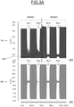
- Figure 3A shows a first graph GR1 illustrating the evolution of the amplitude of the induced signal SIG sent by the reader RD with regard to time, and a second graph GR2 illustrating the evolution of the amplitude of the induced signal SIG received by the tag TG with regard to time.
- first graph GR1 two OOK pulses PL1 and PL2 are sent to the tag TG while the limiter LIM is in said first configuration MODE1.
- the protocol has not yet been detected.
- the first pulse PL1 has a remaining amplitude of 5% of non-modulated signal.
- the second pulse PL2 has a remaining amplitude of 0% of non-modulated signal.
- the first switch SW1 is initially closed to let the resistive capacitive circuit perform a regulation loop operation.
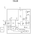
- the limiter LIM being in the first configuration MODE1, the second switch SW2 controlled by said control means CM is off which means that the circuit acting like a Zener diode ZD is coupled in series with the NMOS transistor N1 as shown in figure 3B .
- This first configuration MODE1 reduces the limiter current when the tag TG receives an induced signal SIG with a low amplitude.
- the first configuration MODE1 which isn't adapted to an OOK modulation, leads when the pulse PL1 is sent, to oscillations in the second graph GR2. These oscillations have relatively a high amplitude.
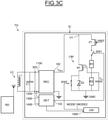
- control means CM close the second switch SW2 to switch to the second configuration MODE2 which is adapted to an OOK modulation.
- the third pulse PL3 has a remaining amplitude of 5% of non-modulated signal.
- the fourth pulse PL4 has also a remaining amplitude of 5% of non-modulated signal.
- the amplitude of said induced signal SIG is proportional to the amplitude of said reader's signal RD.
- the detection level of said detection means DET is put in a lower level which helps to detect the rising edges of the modulated pulses quickly and so the variation of Frame Delay Time will be lower.
- the resistive capacitive circuit When the induced signal SIG modulated according to an ASK modulation is received, the resistive capacitive circuit doesn't react immediately when the amplitude of the induced signal SIG is reduced due to the ASK modulation. Thus, said NMOS transistor N1 continues to drain the same current.
- detection means DET When detection means DET detect the pulses of the ASK modulation, it opens the switch SW1 and the PMOS transistor P1 is disconnected.
- the control voltage V G is maintained because of the capacitor C G , so the gate voltage of the NMOS transistor N1 remains unchanged and the current continues to flow.
- detection means DET detect the pulses of the OOK modulation, it also opens the switch SW1 and the PMOS transistor P1 is disconnected.
Landscapes
- Engineering & Computer Science (AREA)
- Computer Networks & Wireless Communication (AREA)
- Signal Processing (AREA)
- Computer Hardware Design (AREA)
- Microelectronics & Electronic Packaging (AREA)
- Physics & Mathematics (AREA)
- General Physics & Mathematics (AREA)
- Theoretical Computer Science (AREA)
- Computer Security & Cryptography (AREA)
- Digital Transmission Methods That Use Modulated Carrier Waves (AREA)
- Near-Field Transmission Systems (AREA)
Claims (12)
- Procédé pour limiter le niveau d'un signal induit (SIG) reçu par un transpondeur (TG) en provenance d'un lecteur (RD), ledit signal induit (SIG) étant modulé selon un protocole appartenant au groupe qui inclut les protocoles utilisant la modulation par déplacement d'amplitude, ou modulation ASK, et les protocoles utilisant la modulation en tout-ou-rien, ou modulation OOK, ledit procédé comprenant les étapes suivantes :- munir ledit transpondeur (TG) d'un limiteur configurable (LIM) ayant une première configuration (MODE1) adaptée aux protocoles utilisant la modulation ASK, et une seconde configuration (MODE2) adaptée aux protocoles utilisant la modulation OOK ;- mettre ledit limiteur (LIM) dans ladite première configuration (MODE1) jusqu'à ce qu'un protocole soit détecté et si un protocole utilisant la modulation OOK est détecté, faire passer le limiteur de ladite première configuration (MODE1) à ladite seconde configuration (MODE2).
- Procédé selon la revendication 1, dans lequel ledit signal induit est modulé selon un protocole appartenant au groupe qui inclut les protocoles A et B de la norme ISO/IEC14443 et le protocole F de la norme JIS.X.6319, et si le protocole A est détecté, faire passer le limiteur de ladite première configuration (MODE1) à ladite seconde configuration (MODE2).
- Procédé selon la revendication 1 ou 2, dans lequel le signal induit (SIG) a des impulsions modulées et le passage de ladite première configuration (MODE1) à ladite seconde configuration (MODE2) est réalisé avant la réception de la dernière impulsion modulée dudit signal induit (SIG).
- Circuit intégré ayant une entrée configurée pour recevoir un signal induit (SIG), ledit signal induit (SIG) étant modulé selon un protocole appartenant au groupe qui inclut les protocoles utilisant la modulation par déplacement d'amplitude, ou modulation ASK, et les protocoles utilisant la modulation en tout-ou-rien, ou modulation OOK, ledit circuit intégré comprenant :- un moyen de détection (DET) configuré pour détecter ladite modulation ;- un moyen de décodage (DEC) configuré pour détecter ledit protocole ;- un limiteur configurable (LIM) configuré pour limiter le niveau du signal induit et ayant une première configuration (MODE1) adaptée aux protocoles utilisant la modulation ASK et une seconde configuration (MODE2) adaptée aux protocoles utilisant la modulation OOK ;- un moyen de commande (CM) configuré pour mettre le limiteur dans ladite première configuration (MODE1) jusqu'à ce qu'un protocole soit détecté, et configuré pour faire passer le limiteur de ladite première configuration (MODE1) à ladite seconde configuration (MODE2) si un protocole utilisant la modulation OOK est détecté.
- Circuit intégré (IC) selon la revendication 4, dans lequel ledit signal induit est modulé selon un protocole appartenant au groupe qui inclut les protocoles A et B de la norme ISO/IEC14443 et le protocole F de la norme JIS.X.6319, et ledit moyen de commande est configuré pour faire passer le limiteur de ladite première configuration (MODE1) à ladite seconde configuration (MODE2) si le protocole A est détecté.
- Circuit intégré (IC) selon la revendication 4 ou 5, dans lequel le signal induit (SIG) a des impulsions modulées et ledit moyen de commande (CM) est configuré pour réaliser le passage de ladite première configuration (MODE1) à ladite seconde configuration (MODE2) avant que ladite entrée reçoive la dernière impulsion modulée dudit signal induit (SIG).
- Circuit intégré (IC) selon l'une quelconque des revendications 4 à 6, dans lequel, dans ladite première configuration (MODE1), le limiteur est configuré pour réduire un courant de limiteur (LIM) lorsque l'amplitude dudit signal induit (SIG) est réduite.
- Circuit intégré (IC) selon la revendication 7, dans lequel, dans ladite seconde configuration (MODE2), le limiteur est configuré pour ne plus réduire ledit courant de limiteur (LIM) lorsque l'amplitude dudit signal induit (SIG) est réduite.
- Circuit intégré (IC) selon l'une quelconque des revendications 4 à 8, dans lequel, dans ladite seconde configuration (MODE2), le limiteur est configuré pour maintenir inchangée la valeur de son impédance qui a été établie avant que ladite entrée reçoive lesdites impulsions modulées, pendant la réception dudit signal induit (SIG).
- Circuit intégré (IC) selon l'une quelconque des revendications 4 à 9, dans lequel ledit limiteur comprend un transistor NMOS (N1) monté en série avec un premier interrupteur SW2 et un circuit agissant comme une diode Zener entre une borne de tension (VT) et la masse (GND), ledit premier interrupteur SW2 étant commandé par ledit moyen de commande (CM), ledit moyen de commande (CM) étant configuré pour ouvrir ledit premier interrupteur (SW2) dans ladite première configuration (MODE1), et pour fermer ledit premier interrupteur (SW2) dans ladite seconde configuration (MODE2).
- Circuit intégré (IC) selon la revendication 10, comprenant un transistor PMOS (P1) monté en série avec un deuxième interrupteur (SW1) et un circuit capacitif résistif entre ladite borne de tension (VT) et la masse (GND), ledit deuxième interrupteur (SW1) étant commandé par ledit moyen de détection (DET), ledit moyen de détection (DET) étant configuré pour ouvrir ledit deuxième interrupteur (SW1) lorsque le moyen de détection détecte des impulsions modulées dudit signal induit, et étant configuré pour fermer ledit deuxième interrupteur (SW1) lorsqu'un signal non modulé est reçu.
- Transpondeur (TG) comportant un circuit intégré (IC) selon l'une quelconque des revendications 4 à 11.
Priority Applications (4)
| Application Number | Priority Date | Filing Date | Title |
|---|---|---|---|
| EP18178585.8A EP3584949B1 (fr) | 2018-06-19 | 2018-06-19 | Procédé pour limiter le niveau d'un signal modulé reçu par une étiquette et limiteur correspondant |
| US16/442,811 US10984301B2 (en) | 2018-06-19 | 2019-06-17 | Method for limiting the level of a modulated signal received by a tag and corresponding limiter |
| CN201910521335.0A CN110620742B (zh) | 2018-06-19 | 2019-06-17 | 用于限制标签接收的调制信号的电平的方法和对应限制器 |
| CN201920906777.2U CN210075280U (zh) | 2018-06-19 | 2019-06-17 | 集成电路、限制器和应答器 |
Applications Claiming Priority (1)
| Application Number | Priority Date | Filing Date | Title |
|---|---|---|---|
| EP18178585.8A EP3584949B1 (fr) | 2018-06-19 | 2018-06-19 | Procédé pour limiter le niveau d'un signal modulé reçu par une étiquette et limiteur correspondant |
Publications (2)
| Publication Number | Publication Date |
|---|---|
| EP3584949A1 EP3584949A1 (fr) | 2019-12-25 |
| EP3584949B1 true EP3584949B1 (fr) | 2022-01-19 |
Family
ID=62712894
Family Applications (1)
| Application Number | Title | Priority Date | Filing Date |
|---|---|---|---|
| EP18178585.8A Active EP3584949B1 (fr) | 2018-06-19 | 2018-06-19 | Procédé pour limiter le niveau d'un signal modulé reçu par une étiquette et limiteur correspondant |
Country Status (3)
| Country | Link |
|---|---|
| US (1) | US10984301B2 (fr) |
| EP (1) | EP3584949B1 (fr) |
| CN (2) | CN110620742B (fr) |
Families Citing this family (1)
| Publication number | Priority date | Publication date | Assignee | Title |
|---|---|---|---|---|
| CN112202697B (zh) * | 2020-09-30 | 2023-03-21 | 浙江三维通信科技有限公司 | 一种信号的处理方法、装置、存储介质以及电子装置 |
Family Cites Families (13)
| Publication number | Priority date | Publication date | Assignee | Title |
|---|---|---|---|---|
| US6972677B2 (en) * | 2002-08-27 | 2005-12-06 | Coulthard John J | Monitoring system |
| US7313378B2 (en) * | 2003-11-26 | 2007-12-25 | Starkey Laboratories, Inc. | Tracking automatic gain control |
| DE102007040854A1 (de) * | 2007-08-29 | 2009-03-12 | Texas Instruments Deutschland Gmbh | Transponderdemodulator für einen niedrigen Antennenbegrenzerschwellwert |
| US8150270B2 (en) * | 2008-03-31 | 2012-04-03 | Kitel Technologies Llc | Compact high-speed modulator driver method and apparatus |
| JP5295657B2 (ja) * | 2008-06-27 | 2013-09-18 | ルネサスエレクトロニクス株式会社 | 半導体集積回路、半導体集積回路を実装したicカードおよびその動作方法 |
| EP2404394B1 (fr) * | 2009-03-04 | 2016-10-05 | Xieon Networks S.à r.l. | Procédé de traitement de données dans un composant de réseau optique et composant de réseau optique |
| JP5202591B2 (ja) * | 2010-08-26 | 2013-06-05 | 株式会社東芝 | 2値化回路、復調回路、及び車載チューナ |
| FR2977358B1 (fr) * | 2011-06-29 | 2013-08-09 | Gilles Vaquin | Systeme avertisseur de situations dangereuses en milieu agressif |
| US9008230B2 (en) * | 2013-01-08 | 2015-04-14 | Nxp B.V. | Receiver and method for near field communication |
| EP2988427B1 (fr) * | 2014-08-22 | 2019-04-24 | STMicroelectronics International N.V. | Procédé d'étalonnage de phase dans un circuit de pré-amplification d'une communication en champ proche, NFC, dispositif étiquette, circuit de pré-amplification et dispositif d'étiquette NFC |
| SG10201607275YA (en) * | 2016-09-01 | 2018-04-27 | Huawei Int Pte Ltd | Method and device for radio frequency voltage limiting |
| FR3056793A1 (fr) * | 2016-09-29 | 2018-03-30 | Stmicroelectronics (Rousset) Sas | Procede de detection de la presence eventuelle d'un objet par un lecteur sans contact, et lecteur correspondant |
| US10490245B2 (en) * | 2017-10-02 | 2019-11-26 | Micron Technology, Inc. | Memory system that supports dual-mode modulation |
-
2018
- 2018-06-19 EP EP18178585.8A patent/EP3584949B1/fr active Active
-
2019
- 2019-06-17 US US16/442,811 patent/US10984301B2/en active Active
- 2019-06-17 CN CN201910521335.0A patent/CN110620742B/zh active Active
- 2019-06-17 CN CN201920906777.2U patent/CN210075280U/zh not_active Withdrawn - After Issue
Also Published As
| Publication number | Publication date |
|---|---|
| US10984301B2 (en) | 2021-04-20 |
| CN210075280U (zh) | 2020-02-14 |
| EP3584949A1 (fr) | 2019-12-25 |
| CN110620742B (zh) | 2023-09-05 |
| US20190385036A1 (en) | 2019-12-19 |
| CN110620742A (zh) | 2019-12-27 |
Similar Documents
| Publication | Publication Date | Title |
|---|---|---|
| EP2490343B1 (fr) | Dispositif de communication de champ proche | |
| US9305193B2 (en) | Contactless communication device and user device including the same | |
| US11423239B2 (en) | Integrated circuits and methods for protocol detection and decoding in near field communications | |
| KR101765003B1 (ko) | 이중 주파수 hf-uhf 식별 디바이스 | |
| KR20070076071A (ko) | 비접촉식 카드 그리고 비접촉식 카드시스템 | |
| US10044389B2 (en) | Contactless communication device with receiver input voltage stabilization | |
| EP3584949B1 (fr) | Procédé pour limiter le niveau d'un signal modulé reçu par une étiquette et limiteur correspondant | |
| US9912386B2 (en) | Method for operating object capable via contactless communication | |
| US7710213B2 (en) | Method for voltage limitation in a transponder | |
| JP2000049657A (ja) | 無接点伝送システム用アンテナ共振回路装置 | |
| US8207831B2 (en) | Transponder demodulator for a low antenna limiter threshold | |
| EP3267589B1 (fr) | Système de traitement d'un signal d'antenne haute tension dans un circuit intégré | |
| US8328105B2 (en) | Semiconductor device | |
| US8358974B2 (en) | Method and circuit for amplitude modulation of a carrier signal with a specified modulation factor | |
| JP7751471B2 (ja) | オーバーシュートおよびアンダーシュート防止のための波形成形 | |
| CN112069840A (zh) | 应答器以及对应的操作方法 | |
| GB2484104A (en) | Combined regulator and rectifier for a near field RF communicator | |
| Song et al. | A fully integrated HF multi-standard RFID transceiver for compact mobile terminals | |
| KR20030088233A (ko) | 신원 카드 및 신원 카드 시스템 |
Legal Events
| Date | Code | Title | Description |
|---|---|---|---|
| PUAI | Public reference made under article 153(3) epc to a published international application that has entered the european phase |
Free format text: ORIGINAL CODE: 0009012 |
|
| STAA | Information on the status of an ep patent application or granted ep patent |
Free format text: STATUS: THE APPLICATION HAS BEEN PUBLISHED |
|
| AK | Designated contracting states |
Kind code of ref document: A1 Designated state(s): AL AT BE BG CH CY CZ DE DK EE ES FI FR GB GR HR HU IE IS IT LI LT LU LV MC MK MT NL NO PL PT RO RS SE SI SK SM TR |
|
| AX | Request for extension of the european patent |
Extension state: BA ME |
|
| STAA | Information on the status of an ep patent application or granted ep patent |
Free format text: STATUS: REQUEST FOR EXAMINATION WAS MADE |
|
| 17P | Request for examination filed |
Effective date: 20200319 |
|
| RBV | Designated contracting states (corrected) |
Designated state(s): AL AT BE BG CH CY CZ DE DK EE ES FI FR GB GR HR HU IE IS IT LI LT LU LV MC MK MT NL NO PL PT RO RS SE SI SK SM TR |
|
| GRAP | Despatch of communication of intention to grant a patent |
Free format text: ORIGINAL CODE: EPIDOSNIGR1 |
|
| STAA | Information on the status of an ep patent application or granted ep patent |
Free format text: STATUS: GRANT OF PATENT IS INTENDED |
|
| INTG | Intention to grant announced |
Effective date: 20210820 |
|
| GRAS | Grant fee paid |
Free format text: ORIGINAL CODE: EPIDOSNIGR3 |
|
| GRAA | (expected) grant |
Free format text: ORIGINAL CODE: 0009210 |
|
| STAA | Information on the status of an ep patent application or granted ep patent |
Free format text: STATUS: THE PATENT HAS BEEN GRANTED |
|
| AK | Designated contracting states |
Kind code of ref document: B1 Designated state(s): AL AT BE BG CH CY CZ DE DK EE ES FI FR GB GR HR HU IE IS IT LI LT LU LV MC MK MT NL NO PL PT RO RS SE SI SK SM TR |
|
| REG | Reference to a national code |
Ref country code: GB Ref legal event code: FG4D |
|
| REG | Reference to a national code |
Ref country code: CH Ref legal event code: EP |
|
| REG | Reference to a national code |
Ref country code: DE Ref legal event code: R096 Ref document number: 602018029701 Country of ref document: DE |
|
| REG | Reference to a national code |
Ref country code: AT Ref legal event code: REF Ref document number: 1464375 Country of ref document: AT Kind code of ref document: T Effective date: 20220215 |
|
| REG | Reference to a national code |
Ref country code: IE Ref legal event code: FG4D |
|
| REG | Reference to a national code |
Ref country code: LT Ref legal event code: MG9D |
|
| REG | Reference to a national code |
Ref country code: NL Ref legal event code: MP Effective date: 20220119 |
|
| REG | Reference to a national code |
Ref country code: AT Ref legal event code: MK05 Ref document number: 1464375 Country of ref document: AT Kind code of ref document: T Effective date: 20220119 |
|
| PG25 | Lapsed in a contracting state [announced via postgrant information from national office to epo] |
Ref country code: NL Free format text: LAPSE BECAUSE OF FAILURE TO SUBMIT A TRANSLATION OF THE DESCRIPTION OR TO PAY THE FEE WITHIN THE PRESCRIBED TIME-LIMIT Effective date: 20220119 |
|
| PG25 | Lapsed in a contracting state [announced via postgrant information from national office to epo] |
Ref country code: SE Free format text: LAPSE BECAUSE OF FAILURE TO SUBMIT A TRANSLATION OF THE DESCRIPTION OR TO PAY THE FEE WITHIN THE PRESCRIBED TIME-LIMIT Effective date: 20220119 Ref country code: RS Free format text: LAPSE BECAUSE OF FAILURE TO SUBMIT A TRANSLATION OF THE DESCRIPTION OR TO PAY THE FEE WITHIN THE PRESCRIBED TIME-LIMIT Effective date: 20220119 Ref country code: PT Free format text: LAPSE BECAUSE OF FAILURE TO SUBMIT A TRANSLATION OF THE DESCRIPTION OR TO PAY THE FEE WITHIN THE PRESCRIBED TIME-LIMIT Effective date: 20220519 Ref country code: NO Free format text: LAPSE BECAUSE OF FAILURE TO SUBMIT A TRANSLATION OF THE DESCRIPTION OR TO PAY THE FEE WITHIN THE PRESCRIBED TIME-LIMIT Effective date: 20220419 Ref country code: LT Free format text: LAPSE BECAUSE OF FAILURE TO SUBMIT A TRANSLATION OF THE DESCRIPTION OR TO PAY THE FEE WITHIN THE PRESCRIBED TIME-LIMIT Effective date: 20220119 Ref country code: HR Free format text: LAPSE BECAUSE OF FAILURE TO SUBMIT A TRANSLATION OF THE DESCRIPTION OR TO PAY THE FEE WITHIN THE PRESCRIBED TIME-LIMIT Effective date: 20220119 Ref country code: ES Free format text: LAPSE BECAUSE OF FAILURE TO SUBMIT A TRANSLATION OF THE DESCRIPTION OR TO PAY THE FEE WITHIN THE PRESCRIBED TIME-LIMIT Effective date: 20220119 Ref country code: BG Free format text: LAPSE BECAUSE OF FAILURE TO SUBMIT A TRANSLATION OF THE DESCRIPTION OR TO PAY THE FEE WITHIN THE PRESCRIBED TIME-LIMIT Effective date: 20220419 |
|
| PG25 | Lapsed in a contracting state [announced via postgrant information from national office to epo] |
Ref country code: PL Free format text: LAPSE BECAUSE OF FAILURE TO SUBMIT A TRANSLATION OF THE DESCRIPTION OR TO PAY THE FEE WITHIN THE PRESCRIBED TIME-LIMIT Effective date: 20220119 Ref country code: LV Free format text: LAPSE BECAUSE OF FAILURE TO SUBMIT A TRANSLATION OF THE DESCRIPTION OR TO PAY THE FEE WITHIN THE PRESCRIBED TIME-LIMIT Effective date: 20220119 Ref country code: GR Free format text: LAPSE BECAUSE OF FAILURE TO SUBMIT A TRANSLATION OF THE DESCRIPTION OR TO PAY THE FEE WITHIN THE PRESCRIBED TIME-LIMIT Effective date: 20220420 Ref country code: FI Free format text: LAPSE BECAUSE OF FAILURE TO SUBMIT A TRANSLATION OF THE DESCRIPTION OR TO PAY THE FEE WITHIN THE PRESCRIBED TIME-LIMIT Effective date: 20220119 Ref country code: AT Free format text: LAPSE BECAUSE OF FAILURE TO SUBMIT A TRANSLATION OF THE DESCRIPTION OR TO PAY THE FEE WITHIN THE PRESCRIBED TIME-LIMIT Effective date: 20220119 |
|
| PG25 | Lapsed in a contracting state [announced via postgrant information from national office to epo] |
Ref country code: IS Free format text: LAPSE BECAUSE OF FAILURE TO SUBMIT A TRANSLATION OF THE DESCRIPTION OR TO PAY THE FEE WITHIN THE PRESCRIBED TIME-LIMIT Effective date: 20220519 |
|
| REG | Reference to a national code |
Ref country code: DE Ref legal event code: R097 Ref document number: 602018029701 Country of ref document: DE |
|
| PG25 | Lapsed in a contracting state [announced via postgrant information from national office to epo] |
Ref country code: SM Free format text: LAPSE BECAUSE OF FAILURE TO SUBMIT A TRANSLATION OF THE DESCRIPTION OR TO PAY THE FEE WITHIN THE PRESCRIBED TIME-LIMIT Effective date: 20220119 Ref country code: SK Free format text: LAPSE BECAUSE OF FAILURE TO SUBMIT A TRANSLATION OF THE DESCRIPTION OR TO PAY THE FEE WITHIN THE PRESCRIBED TIME-LIMIT Effective date: 20220119 Ref country code: RO Free format text: LAPSE BECAUSE OF FAILURE TO SUBMIT A TRANSLATION OF THE DESCRIPTION OR TO PAY THE FEE WITHIN THE PRESCRIBED TIME-LIMIT Effective date: 20220119 Ref country code: EE Free format text: LAPSE BECAUSE OF FAILURE TO SUBMIT A TRANSLATION OF THE DESCRIPTION OR TO PAY THE FEE WITHIN THE PRESCRIBED TIME-LIMIT Effective date: 20220119 Ref country code: DK Free format text: LAPSE BECAUSE OF FAILURE TO SUBMIT A TRANSLATION OF THE DESCRIPTION OR TO PAY THE FEE WITHIN THE PRESCRIBED TIME-LIMIT Effective date: 20220119 Ref country code: CZ Free format text: LAPSE BECAUSE OF FAILURE TO SUBMIT A TRANSLATION OF THE DESCRIPTION OR TO PAY THE FEE WITHIN THE PRESCRIBED TIME-LIMIT Effective date: 20220119 |
|
| PLBE | No opposition filed within time limit |
Free format text: ORIGINAL CODE: 0009261 |
|
| STAA | Information on the status of an ep patent application or granted ep patent |
Free format text: STATUS: NO OPPOSITION FILED WITHIN TIME LIMIT |
|
| PG25 | Lapsed in a contracting state [announced via postgrant information from national office to epo] |
Ref country code: AL Free format text: LAPSE BECAUSE OF FAILURE TO SUBMIT A TRANSLATION OF THE DESCRIPTION OR TO PAY THE FEE WITHIN THE PRESCRIBED TIME-LIMIT Effective date: 20220119 |
|
| 26N | No opposition filed |
Effective date: 20221020 |
|
| PG25 | Lapsed in a contracting state [announced via postgrant information from national office to epo] |
Ref country code: MC Free format text: LAPSE BECAUSE OF FAILURE TO SUBMIT A TRANSLATION OF THE DESCRIPTION OR TO PAY THE FEE WITHIN THE PRESCRIBED TIME-LIMIT Effective date: 20220119 |
|
| REG | Reference to a national code |
Ref country code: CH Ref legal event code: PL |
|
| REG | Reference to a national code |
Ref country code: BE Ref legal event code: MM Effective date: 20220630 |
|
| PG25 | Lapsed in a contracting state [announced via postgrant information from national office to epo] |
Ref country code: SI Free format text: LAPSE BECAUSE OF FAILURE TO SUBMIT A TRANSLATION OF THE DESCRIPTION OR TO PAY THE FEE WITHIN THE PRESCRIBED TIME-LIMIT Effective date: 20220119 |
|
| GBPC | Gb: european patent ceased through non-payment of renewal fee |
Effective date: 20220619 |
|
| PG25 | Lapsed in a contracting state [announced via postgrant information from national office to epo] |
Ref country code: LU Free format text: LAPSE BECAUSE OF NON-PAYMENT OF DUE FEES Effective date: 20220619 Ref country code: LI Free format text: LAPSE BECAUSE OF NON-PAYMENT OF DUE FEES Effective date: 20220630 Ref country code: IE Free format text: LAPSE BECAUSE OF NON-PAYMENT OF DUE FEES Effective date: 20220619 Ref country code: FR Free format text: LAPSE BECAUSE OF NON-PAYMENT OF DUE FEES Effective date: 20220630 Ref country code: CH Free format text: LAPSE BECAUSE OF NON-PAYMENT OF DUE FEES Effective date: 20220630 |
|
| PG25 | Lapsed in a contracting state [announced via postgrant information from national office to epo] |
Ref country code: GB Free format text: LAPSE BECAUSE OF NON-PAYMENT OF DUE FEES Effective date: 20220619 Ref country code: BE Free format text: LAPSE BECAUSE OF NON-PAYMENT OF DUE FEES Effective date: 20220630 |
|
| PG25 | Lapsed in a contracting state [announced via postgrant information from national office to epo] |
Ref country code: IT Free format text: LAPSE BECAUSE OF FAILURE TO SUBMIT A TRANSLATION OF THE DESCRIPTION OR TO PAY THE FEE WITHIN THE PRESCRIBED TIME-LIMIT Effective date: 20220119 |
|
| PG25 | Lapsed in a contracting state [announced via postgrant information from national office to epo] |
Ref country code: MK Free format text: LAPSE BECAUSE OF FAILURE TO SUBMIT A TRANSLATION OF THE DESCRIPTION OR TO PAY THE FEE WITHIN THE PRESCRIBED TIME-LIMIT Effective date: 20220119 Ref country code: CY Free format text: LAPSE BECAUSE OF FAILURE TO SUBMIT A TRANSLATION OF THE DESCRIPTION OR TO PAY THE FEE WITHIN THE PRESCRIBED TIME-LIMIT Effective date: 20220119 |
|
| PG25 | Lapsed in a contracting state [announced via postgrant information from national office to epo] |
Ref country code: HU Free format text: LAPSE BECAUSE OF FAILURE TO SUBMIT A TRANSLATION OF THE DESCRIPTION OR TO PAY THE FEE WITHIN THE PRESCRIBED TIME-LIMIT; INVALID AB INITIO Effective date: 20180619 |
|
| REG | Reference to a national code |
Ref country code: DE Ref legal event code: R081 Ref document number: 602018029701 Country of ref document: DE Owner name: STMICROELECTRONICS INTERNATIONAL N.V., PLAN-LE, CH Free format text: FORMER OWNER: STMICROELECTRONICS RAZVOJ POLPREVODNIKOV D.O.O., LJUBLJANA, SI |
|
| PG25 | Lapsed in a contracting state [announced via postgrant information from national office to epo] |
Ref country code: MT Free format text: LAPSE BECAUSE OF FAILURE TO SUBMIT A TRANSLATION OF THE DESCRIPTION OR TO PAY THE FEE WITHIN THE PRESCRIBED TIME-LIMIT Effective date: 20220119 |
|
| PGFP | Annual fee paid to national office [announced via postgrant information from national office to epo] |
Ref country code: DE Payment date: 20250520 Year of fee payment: 8 |
|
| PG25 | Lapsed in a contracting state [announced via postgrant information from national office to epo] |
Ref country code: TR Free format text: LAPSE BECAUSE OF FAILURE TO SUBMIT A TRANSLATION OF THE DESCRIPTION OR TO PAY THE FEE WITHIN THE PRESCRIBED TIME-LIMIT Effective date: 20220119 |