EP3588040B1 - Dehnelement und kraftsensor mit dehnelement - Google Patents
Dehnelement und kraftsensor mit dehnelement Download PDFInfo
- Publication number
- EP3588040B1 EP3588040B1 EP17897602.3A EP17897602A EP3588040B1 EP 3588040 B1 EP3588040 B1 EP 3588040B1 EP 17897602 A EP17897602 A EP 17897602A EP 3588040 B1 EP3588040 B1 EP 3588040B1
- Authority
- EP
- European Patent Office
- Prior art keywords
- strain
- electrode
- central portion
- connecting portion
- sensors
- Prior art date
- Legal status (The legal status is an assumption and is not a legal conclusion. Google has not performed a legal analysis and makes no representation as to the accuracy of the status listed.)
- Not-in-force
Links
Images






Classifications
-
- G—PHYSICS
- G01—MEASURING; TESTING
- G01L—MEASURING FORCE, STRESS, TORQUE, WORK, MECHANICAL POWER, MECHANICAL EFFICIENCY, OR FLUID PRESSURE
- G01L1/00—Measuring force or stress, in general
- G01L1/20—Measuring force or stress, in general by measuring variations in ohmic resistance of solid materials or of electrically-conductive fluids; by making use of electrokinetic cells, i.e. liquid-containing cells wherein an electrical potential is produced or varied upon the application of stress
- G01L1/22—Measuring force or stress, in general by measuring variations in ohmic resistance of solid materials or of electrically-conductive fluids; by making use of electrokinetic cells, i.e. liquid-containing cells wherein an electrical potential is produced or varied upon the application of stress using resistance strain gauges
-
- B—PERFORMING OPERATIONS; TRANSPORTING
- B25—HAND TOOLS; PORTABLE POWER-DRIVEN TOOLS; MANIPULATORS
- B25J—MANIPULATORS; CHAMBERS PROVIDED WITH MANIPULATION DEVICES
- B25J13/00—Controls for manipulators
- B25J13/08—Controls for manipulators by means of sensing devices, e.g. viewing or touching devices
- B25J13/085—Force or torque sensors
-
- G—PHYSICS
- G01—MEASURING; TESTING
- G01L—MEASURING FORCE, STRESS, TORQUE, WORK, MECHANICAL POWER, MECHANICAL EFFICIENCY, OR FLUID PRESSURE
- G01L1/00—Measuring force or stress, in general
- G01L1/20—Measuring force or stress, in general by measuring variations in ohmic resistance of solid materials or of electrically-conductive fluids; by making use of electrokinetic cells, i.e. liquid-containing cells wherein an electrical potential is produced or varied upon the application of stress
- G01L1/22—Measuring force or stress, in general by measuring variations in ohmic resistance of solid materials or of electrically-conductive fluids; by making use of electrokinetic cells, i.e. liquid-containing cells wherein an electrical potential is produced or varied upon the application of stress using resistance strain gauges
- G01L1/2287—Measuring force or stress, in general by measuring variations in ohmic resistance of solid materials or of electrically-conductive fluids; by making use of electrokinetic cells, i.e. liquid-containing cells wherein an electrical potential is produced or varied upon the application of stress using resistance strain gauges constructional details of the strain gauges
-
- G—PHYSICS
- G01—MEASURING; TESTING
- G01L—MEASURING FORCE, STRESS, TORQUE, WORK, MECHANICAL POWER, MECHANICAL EFFICIENCY, OR FLUID PRESSURE
- G01L5/00—Apparatus for, or methods of, measuring force, work, mechanical power, or torque, specially adapted for specific purposes
- G01L5/16—Apparatus for, or methods of, measuring force, work, mechanical power, or torque, specially adapted for specific purposes for measuring several components of force
- G01L5/161—Apparatus for, or methods of, measuring force, work, mechanical power, or torque, specially adapted for specific purposes for measuring several components of force using variations in ohmic resistance
- G01L5/1627—Apparatus for, or methods of, measuring force, work, mechanical power, or torque, specially adapted for specific purposes for measuring several components of force using variations in ohmic resistance of strain gauges
Definitions
- Embodiments of the present invention described herein relate generally to, for example, a six-axis force sensor, etc., provided with a strain body and applicable to a robot arm.
- Patent Literature 1 and Patent Literature 2 Six-axis force sensors which are used in, for example, robot arms, to detect an external force and torque in X, Y, and Z directions have been known (refer to, for example, Patent Literature 1 and Patent Literature 2).
- a force sensor In such a force sensor, an external force applied to a force receiving body serving as a movable unit is transmitted to a strain body, and deformation of a strain sensor (strain gauge) provided on the strain body is converted into an electric signal and detected.
- a strain sensor strain gauge
- the range of application of the strain body provided with such a strain sensor tends to extend in accordance with development of computer technologies and information communication technologies of these days, and further downsizing and higher performance of the strain body are required.
- the strain bodies according to Patent Literature 3 and 4 do not disclose the following features: an electrode provided on a main surface of the central portion and electrically connected to the strain sensors and the reference resistors to take a detection signal of the bridge circuit as well as an anisotropic conductive film provided between the electrode and the lead wire to make electric connection between a terminal of the electrode and a terminal of the lead wire.
- Embodiments of the present invention described herein can provide a strain body and a force sensor provided with the strain body, capable of improving reliability while securing reliable electric connection between an electrode terminal and a terminal of a lead wire.
- a strain body and a force sensor provided with the strain body capable of improving reliability while securing reliable electric connection between an electrode terminal and a terminal of a lead wire can be provided.
- FIG. 1 is a perspective view showing the whole structure of the strain body according to the first embodiment.
- FIG. 2 is a plan view showing the planar structure of the strain body in FIG. 1 .
- a strain body 16 As shown in FIG. 1 and FIG. 2 , a strain body 16 according to the first embodiment comprises a central portion 161, an outer peripheral portion 162 which surrounds the periphery of the central portion 161, and four connecting portions 163 which connect the central portion 161 and the outer peripheral portion 162.
- the strain body 16 is formed of, for example, a predetermined metal such as stainless steel.
- the central portion 161 includes a center O, which is the intersection of two diagonal lines L1 connecting the corner portions of the outer peripheral portion 162.
- a plurality of reference resistors for constructing bridge circuits which will be described later, are provided in the central portion 161.
- Four screw holes 18a for fixing a first support member which is an external member are provided in the corner portions of the central portion 161.
- Each of the screw holes 18a is provided to protrude in a hollow portion OP1 from the center O side to the outside along the directions of the diagonal lines L1 for the purpose of saving space.
- screw holes 17a for fixing a second support member different from the first support member which is an external member are provided in the corner portions of the outer peripheral portion 162.
- Each of the screw holes 17a is provided to protrude in the hollow portion OP1 from the outside to the center O side along the directions of the diagonal lines L1 for the purpose of saving space.
- connecting portions 163 are provided radially from the center O along the X direction or Y direction.
- a plurality of strain sensors for detecting external force and torque in X, Y, and Z directions, which are not shown in the drawings, are provided in the connecting portions 163.
- the width of the connecting portions 163 is formed to be approximately the same from the center O side toward the outside.
- the height Hz of the strain body 16 along the Z direction is common to the central portion 161, the outer peripheral portion 162, and the connecting portions 163, the height is substantially the same.
- the height Hz of the strain body 16 is formed to be greater than the width W162 of the outer peripheral portion 162 along the X direction or the Y direction (Hz>W162).
- the elasticity of the outer peripheral portion 162 and the connecting portions 163 is formed to be greater than the elasticity of the central portion 161. More desirably, the outer peripheral portion 162 and the connecting portions 163 are formed to have an elastic function, and the central portion 161 is formed to have no elastic function.
- the elastic function means a function of causing elastic deformation with input external force and torque.
- the amount of strain of the elastic deformation of the central portion 161 is, preferably, less than or equal to 3 ⁇ 10 -6 at a rated load, and more preferably, less than or equal to 1 ⁇ 10 -6 .
- the elastic deformation of the connecting portions (beam portions) 163 is within the elastic limit of a material at a rated load, and the strain amount is, desirably, greater than or equal to 2 ⁇ 10 -5 , and more desirably, greater than or equal to 2 ⁇ 10 -4 .
- the elastic deformation of the outer peripheral portion 162 is within the elastic limit of a material at a rated load, and the amount of flexure of the most flexed portion is, preferably, greater than or equal to 20 ⁇ m, and more desirably, greater than or equal to 50 ⁇ m.
- FIG. 3 is a plan view showing the central portion 161 and the connecting portions 163 from the perspective of the main surface side of the strain body 16, on which the strain sensors, etc., are provided, in detail.
- strain sensors S1 to S32 are metallic thin-film resistive elements as described later and are, for example, resistive elements (Cr-N resistive elements) including chromium (Cr) and nitrogen (N). For this reason, the plurality of strain sensors S1 to S32 can be disposed at desired positions only by patterning as described later. In addition, since the temperature coefficients of the Cr-N resistive elements are small, temperature compensation can easily be made.
- the longitudinal direction of the strain sensors S1 to S32 is made to coincide with the X direction or the Y direction.
- Reference resistors RS4, RS6, RS12, RS14, RS20, RS22, RS28, and RS30 are provided on the main surface of the central portion 161.
- the shape and material of the reference resistors RS4 to RS30 are substantially the same as those of the strain sensors S1 to S32, and their longitudinal direction is made to coincide with the X direction or the Y direction.
- an electrode 171 is provided along one of the directions of the diagonal lines L1 of the central portion 161, on the main surface of the central portion 161.
- a wire 172 is arranged on the main surface such that the strain sensors and the reference resistors construct four bridge circuits as described later and that the strain sensors construct four full-bridge circuits as described later.
- the wire 172 is electrically connected to a predetermined terminal of the electrode 171.
- the line width of the wire 172 is formed to be smaller at portions connecting the strain sensors S1 to S32 and the reference resistors RS4 to RS30 and to be larger than the connecting portions to reduce the line resistance at the other portions.
- the strain sensors S1 to S32, the reference resistors RS4 to RS30, the electrode 171, and the wire 172 are integrally formed on the main surface of the strain body 16 by a manufacturing method employing a thin-film technique as described later. For this reason, the strain sensors S1 to S32, the reference resistors RS4 to RS30, the electrode 171, and the wire 172 are formed in a layout of being symmetrical on both sides of the diagonal lines L1 of the strain body 16.
- FIG. 4 is a cross-sectional view of the connecting portion 163 including the strain sensor S1 in FIG. 3 .
- an insulating film 170 is provided on the main surface of the connecting portion 163.
- the strain sensor S1 which is a Cr-N resistive element serving as a strain sensitive film, is provided on the insulating film 170.
- the wire 172 which is an electrode lead film formed of copper (Cu), is provided on the strain sensor S1.
- An overglass (OG) film 175 is provided so as to cover the strain sensor S1 and the wire 172.
- an adhesive film 172a containing chromium (Cr) to improve adhesion is provided on the interface between the wire 172 and the strain sensor S1 and the interface between the wire 172 and the OG film 175.
- the electrode 171 connected to the wire 172 at the central portion 161 is formed of a multilayer structure of copper (Cu) and gold (Au) sequentially provided on an adhesive film 172a, though not illustrated in the cross-section.
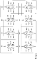
- FIG. 5 is a circuit diagram showing bridge circuits and full-bridge circuits of the strain body 16 according to the first embodiment.
- the strain body 16 comprises four bridge circuits BF2, BF4, BF6, and BF8 and four full-bridge circuits BF1, BF3, BF5, and BF7.
- the bridge circuit BF2 comprises two strain sensors (first strain sensors) S3 and S5 and two reference resistors RS4 and RS6.
- the strain sensor S3 and the reference resistor RS4 are connected in series, and the reference resistor RS6 and the strain sensor S5 are connected in series, between the power supply terminal E and the ground G.
- the strain sensor S3 and the reference resistor RS4, which are connected in series, and the reference resistor RS6 and the strain sensor S5, which are connected in series, are connected in parallel between a power supply terminal E and a ground G.
- a terminal V- is connected to a connection between the strain sensor S3 and the reference resistor RS4.
- the other terminal V+ is connected to a connection between the reference resistor RS6 and the strain sensor S5.
- the other bridge circuits BF4, BF6, and BF8 also are constructed similarly to the bridge circuit BF2.
- the full-bridge circuit BF1 is composed of four strain sensors (second strain sensors) S1, S2, S7, and S8.
- the strain sensor S1 and the strain sensor S2 are connected in series, and the strain sensor S7 and the strain sensor S8 are connected in series, between the power supply terminal E and the ground G.
- the strain sensors S1 and S2, which are connected in series, and the strain sensors S7 and S8, which are connected in series, are connected in parallel between the power supply terminal E and the ground G.
- a terminal V- is connected to a connection between the strain sensors S1 and S2.
- the other terminal V+ is connected to a connection between the strain sensors S7 and S8.
- the other full-bridge circuits BF3, BF5, and BF7 are constructed similarly to the full-bridge circuit BF1.
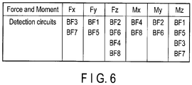
- FIG. 6 is a figure showing a relationship between a detection circuit and the detected force and moment.
- the full-bridge circuits BF3 and BF7 detect force Fx in the X direction and moment Mz in the Z direction.
- the full-bridge circuits BF1 and BF5 detect force Fy in the Y direction and moment Mz in the Z direction.
- the bridge circuits BF2 and BF6 detect force Fz in the Z direction and moment My in the Y direction.
- the bridge circuits BF4 and BF8 detect force Fz in the Z direction and moment Mx in the X direction.
- FIG. 7 is a flowchart for explanation of the method of manufacturing the strain body 16 according to the first embodiment.
- the strain body 16 is first subjected to a test of the dimensions or the like, a predetermined test is preformed, and then, pretreatment is performed for the strain body 16 (B1).
- the pretreatment includes, for example, washing treatment of the main surface of the strain body 16 after the test with ultrasonic waves, a predetermined agent, and the like.
- the insulating film 170 is formed on the main surface of the strain body 16 after the pretreatment by, for example, a thermal oxidation method (B2).
- the strain body 16 is subjected to heat treatment such as a predetermined annealing treatment, such that properties such as an insulation property, of the formed insulating film 170, are improved (B3).
- a Cr-N thin film containing chromium (Cr) and nitrogen (N) is formed on the insulating film 170 by, for example, a sputtering using a predetermined target. Moreover, a photoresist is coated on the formed Cr-N thin film, and the coated photoresist is subjected to patterning.
- a pattern having the same planar shape as that of the reference resistors RS4 to RS30 is transferred to the photoresist at the position where the reference resistors RS4 to RS30 of the central portion 161 are disposed
- the pattern having the same planar shape as the strain sensors S1 to S32 is transferred to the photoresist at the position where the strain sensors S1 to S32 of the connecting portion 163 are disposed, and the photoresist other than the portions where these patterns are transferred is removed by development.
- etching is performed to the surface of the insulating film 170 using the photoresist on which the pattern is developed as a mask, and the reference resistors RS4 to RS30 and the strain sensors S1 to S32 having desired shapes are thereby formed at predetermined positions on the central portion 161 and the connecting portion 163 (B4).
- an adhesive film 172a of a chromium (Cr) thin film for enhancing adhesion is formed on the central portion 161 and the connecting portion 163 using, for example, the same manufacturing process as step B4, etc.
- An electrode lead film containing copper (Cu) is formed on the adhesive film 172a, and a wire 172 for electric connection between the strain sensors S1 to S32 and the reference resistors RS4 to RS30 is formed.
- an adhesive film 172a composed of chromium thin film is formed on the wire 172 by the same manufacturing process as the above-described step (B5) .
- an electrode 171 serving as an electrode film is formed in a direction along the direction of one diagonal line L1, on the adhesive film 172a at the end part of the wire 172 in the central portion 161, as shown in FIG. 3 .
- the electrode 171 is formed by sequentially forming a stacked structure composed of copper (Cu) and gold (Au) by using, for example, the same manufacturing process as step B4 (B6) .
- the OG film 175 is formed on the main surface of the strain body 16 except on the electrode 171 by using, for example, a Chemical Vapor Deposition (CVD) method (B7).
- CVD Chemical Vapor Deposition
- strain sensors S1 to S32 and the like formed on the main surface of the strain body 16 are subjected to strain properties inspection, stress inspection and the like, to confirm the characteristics required for the strain sensors S1 to S32 and the like (B8) .
- the strain body 16 according to the first embodiment is manufactured by the above manufacturing method.
- the strain body 16 is provided on the main surface of the central portion 161 substantially free from distortion, and comprises a plurality of reference resistors RS4 to RS30 constructing the bridge circuits BF2, BF4, BF6, and BF8 together with the plurality of strain sensors S1 to S32 ( FIG. 3 ).
- the reference resistors RS4 to RS30 are integrally provided on the main surface of the same strain body 16 as the strain sensors S1 to S32.
- the strain body 16 according to the first embodiment is provided on the main surface of the connecting portion 163, and comprises the full bridge circuits BF2, BF4, BF6, and BF8 in which a pair of serially connected strain sensors (second strain sensors) are connected in parallel ( FIG. 5 ).
- the sensitivity of the strain body 16 can be improved, and the detection accuracy can be improved.
- the sensitivity and detection accuracy can be improved up to approximately twice as compared to the case where all the detection circuits are composed of bridge circuits.
- the layout of the strain sensors S1 to S32, the reference resistors RS4 to RS30, the electrodes 171, and the wire 172 is formed symmetrically about the diagonal line L1 of the strain body 16.
- the width of the connecting portion 163 is formed to be substantially the same from the center O side to the outer side, space to arrange the strain sensors S1 to S32 can be extended as compared to a configuration in which the width decreases from the center O to the outer side ( FIG. 3 ).
- the strain body 16 according to the first embodiment has an optimum configuration for arranging the strain sensors S1 to S32 and the like in a limited space on the main surface of the central portion 161 and the connecting portion 163.
- strain sensors S1 to S32, the reference resistors RS4 to RS30, the electrode 171, and the wire 172 are provided only on the main surface of strain body 16 by a manufacturing method using the thin film technology ( FIG. 4 and FIG. 7 ).
- high sensitivity sensors S1 to S32 can be provided at the connecting portion 163 of the strain body 16 with high density and high accuracy. Therefore, a large number of (for example, approximately ninety) strain sensors do not need to be arranged to compensate for the detection accuracy, and the strain sensors do not need to be applied on not only the surface of the strain body but also, for example, the side surfaces of the strain body, by using an adhesive or the like.
- the position of the strain sensor may cause an error of approximately several hundreds of ⁇ m from the desired position. For this reason, influence of multiaxial interference in which forces and torques other than the specific axis are detected increases.
- the temperature error and the external noise also need to be corrected since the temperature error and the external noise increase. In the present embodiment, however, such a problem does not occur.
- the height Hz of the strain body 16 along the Z direction is substantially the same in the central portion 161, the outer peripheral portion 162, and the connecting portion 163.
- the height Hz of the strain body 16 is formed to be greater than the width W162 of the outer peripheral portion 162 along the X direction or the Y direction (Hz>W162).
- the elasticity of the outer peripheral portion 162 and the connecting portions 163 is formed to be greater than the elasticity of the central portion 163. More desirably, the outer peripheral portion 162 and the connecting portion 163 are configured to have an elastic function and not to have the elastic function of the central portion 163.
- FIG. 8 is a perspective view showing an overall structure of a strain body 16A according to a second embodiment as viewed from its back side.
- FIG. 9 is an enlarged cross-sectional view showing a strain increasing portion surrounded by a broken line in FIG. 8 .
- the connecting portion 163 of the strain body 16A comprises a first connecting portion 163a adjacent to the outer peripheral portion 162 and a second connecting portion 163b adjacent to the central portion 161.
- the first connecting portion 163a is provided on the back surface side with a strain increasing portion GR for increasing the strain generated more than the second connecting portion 163b. That is, the strain increasing portion GR is configured such that the strain generated in the first connection portion 163a is larger than the strain generated in the second connecting portion 163b.
- the strain increasing portion GR is a groove formed in a substantially U shape, at a part of the back surface side of the first connecting portion 163a. More specifically, since the groove is formed such that its thickness becomes larger from the center of the groove toward the outer peripheral portion 162 and the central portion 161, the first connecting portion 163a is shaped in an arch which is recessed in the thickness direction (Z direction) of the strain body 16.
- the height Hg from the back surface of the strain increasing portion GR and the length Lg of the first connecting portion 163a can be appropriately set under conditions that the first connecting portion 163a is not plastically deformed when force and torque are applied.
- the height Hg of the strain increasing portion GR from the back surface is, desirably, for example, approximately 30% or more and 60% or less of the height Hz of the strain body 16.
- the length Lg of the strain increasing portion GR is, desirably, for example, approximately 30% or more and 70% or less of the entire length L163 of the connecting portion 163.
- the width W163 of the connecting portion 163 is the same in the first and second connecting portions 163a and 163b.
- first strain sensors S21 and the like that construct the bridge circuit are provided in the first connecting portion 163a.
- the second connecting portion 163b is provided with sixteen strain sensors (second strain sensors) S18, S27, and the like that construct the full bridge circuit. The details will be explained in detail with reference to FIG. 10 .
- FIG. 10 is a plan view showing an overall structure of the strain body 16A according to the second embodiment as viewed from its main surface side.
- illustration of the electrode, the wire, and the like is omitted.
- strain sensors (first strain sensors) S3, S5, S11, S13, S19, S21, S27, and S29 constructing the bridge circuits BF2, BF4, BF6, and BF8 are provided at the first connecting portion 163a.
- sixteen strain sensors (second strain sensors) S1, S2, S7, S8, S9, S10, S15, S16, S17, S18, S23, S24, S25, S26, S31, and S32 which construct the full bridge circuits BF1, BF3, BF5, and BF7 are provided.
- Eight strain sensors S1, S2, S15, S16, S17, S18, S25, and S26, of the second strain sensors provided in the second connecting portion 163b, are arranged adjacent to the grooves GR as compared with the other second strain sensors. For this reason, in the second strain sensors S1 and the like, too, the strain amount is increased and the sensor sensitivity is increased, similarly to the first strain sensor provided in the first connecting portion 163a.
- strain body 16A of the second embodiment According to the structure and the operation of the strain body 16A of the second embodiment, at least similar functions and advantages as those of the first embodiment can be obtained.
- the strain body 16A according to the second embodiment further comprises the strain increasing portion GR for increases the generated strain generated more than the second connecting portion 163b adjacent to the central portion 161, on the back surface side of each first connecting portion 163a adjacent to the outer peripheral portion 162.
- the strain increasing portion GR is a U-shaped groove provided at a part of the back surface of the first connecting portion 163a ( FIG. 8 and FIG. 9 ).
- the thickness of the first connecting portion 163a provided with the strain increasing portion GR is smaller than the thickness of the second connecting portion 163b, the amount of deformation of the first connecting portion 163a can be increased as compared to the amount of deformation of the second connecting portion 163a, when force and torque are applied from the outside to the strain body 16A.
- Eight first strain sensors S3 and the like provided in the first connecting portions 163a construct four bridge circuits BF2, BF4, BF6, and BF8 together with eight reference resistors RS4 and the like ( FIG. 10 ). For this reason, according to the strain body 16A according to the second embodiment, the detection accuracy of four bridge circuits BF2, BF4, BF6, and BF8 can be further improved by increasing the strain amount of the eight first strain sensors S3 and the like provided in the first connecting portion 163a.
- strain sensors S1, S2, S15, S16, S17, S18, S25, and S26, of the second strain sensors provided in the second connecting portion 163b are arranged adjacent to the grooves GR as compared with the other second strain sensors. For this reason, the strain amount is increased in the second strain sensors S1 and the like, similarly to the first strain sensors provided in the first connecting portion 163a. Therefore, the detection accuracy of the four full bridge circuits BF1, BF3, BF5, and BF7 constructed by the eight strain sensors S1 and the like can be further improved. As a result, the detection accuracy in all the six axial directions related to the force and torque in the XYZ-axis directions can be improved.
- the strain amount of the eight strain sensors S3 and the like provided in the first connecting portion 163a can be increased by approximately 50% as compared with the strain sensors S3 and the like according to the first embodiment. Therefore, the desired detection accuracy can be obtained by employing the strain body 16A according to the second embodiment as needed.
- the third embodiment relates to an example of application of the strain body 16 according to the first embodiment to a force sensor.
- the force sensor according to the third embodiment is used in, for example, a robot arm, and is a six-axis force sensor for detecting force and torque in X, Y, and Z directions.
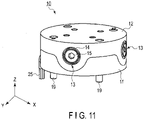
- FIG. 11 is a perspective view showing an appearance of a force sensor 10 provided with the strain body 16 according to the first embodiment.
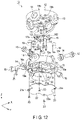
- FIG. 12 is an exploded perspective view showing the force sensor 10 in FIG. 11 .
- the force sensor 10 comprises a cylindrical main body 11 and a cylindrical movable body 12 which is movable with respect to the main body 11.
- the main body 11 is fixed to a main body of a robot arm not shown in the figures with a plurality of screws 19 inserted in a plurality of screw holes 19a formed in the bottom of the main body 11.
- the movable body 12 functions as a hand mounting plate for mounting a hand portion of the robot art not shown in the figures on its top surface.
- the main body (base) 11 is a base member serving as the main body of the force sensor 10, and the movable body 12 is mounted so as to be movable in six-axis directions (an X-axis direction, a Y-axis direction, a Z-axis direction, and directions of rotation around the axes) with respect to the main body 10 with the strain body 16, which is elastically deformable, interposed therebetween.
- a central portion 161 of the strain body 16 is fixed to the movable body (first support member) 12 with a plurality of screws 18 inserted in screw holes 18a.
- An outer peripheral portion 162 of the strain body 16 is fixed to the main body 11 (second support member) with a plurality of screws 17 inserted in screw holes 17a.
- the main surface and the back surface of the strain body 16 are disposed in parallel to a plane formed by the X axis and the Y axis, and a line perpendicularly passing through a center O of the strain body 16 corresponds to the Z axis.
- the movable body 12 moves, and connecting portions 163 of the strain body 16 are deformed.
- strain sensors S1 to S32 are provided in the connecting portions 163 of the strain body 16, and the deformation of the strain body 16 is thereby detected as an electrical signal by the strain sensors S1 to S32.
- opening portions 13 are provided at regular intervals, in the peripheral surface of the movable body 12. That is, the opening portions 13 are disposed in the X-axis direction and the Y-axis direction.
- the number of opening portions 13 is not limited to four, and may be any number greater than or equal to three.
- Stoppers 14 are disposed inside the opening portions 13, respectively, and the stoppers 14 are fixed to the main body 11 with bolts 15, respectively.
- the stoppers 14 regulate the movement range of the movable body 12, and the outermost peripheral portions of the stoppers 14 are provided with first side surfaces 14a which the inner surfaces of the opening portions 13 can contact. That is, on the first side surface 14a, when the strain body 16 is deformed with the movement of the movable body 12, the inner surfaces of the opening portions 13 of the movable body 12 contact the first side surfaces 14a and function as protective mechanisms for protecting excessive deformation of the connecting portions 163 of the strain body 16.
- a substrate 20 is provided in the main body 11 so as to face the strain body 16.
- the substrate 20 comprises a plurality of holes 21a, and is fixed to the main body 11 with fixing screws 21 inserted in the screw holes 21a, respectively.
- the substrate 20 is electrically connected to strain sensors and the like provided on the strain body 16. The details will be described later.
- a cover 22 closing an opening portion 11a is attached to the bottom of the main body 11. That is, the cover 22 comprises a plurality of screw holes 23a, and is fixed to the main body 11 with screws 23 inserted in the screw holes 23a, respectively.
- a wire 25 for transmitting a detection signal to the outside is drawn to the side surface of the main body 11.
- the wire 25 is electrically connected to the substrate 20.
- FIG. 13 is a cross-sectional view showing the strain body 16 in the state of being mounted in the force sensor 10.
- an insulating film 170 is provided on the main surface of the strain body 16, and an electrode 171 is provided on the insulating film 170. Furthermore, an anisotropic conductive film (ACF) 181 is provided on the electrode 171 to be mounted in the force sensor 10.
- a lead wire 182 for electrically connecting the electrode 171 and the substrate 20 is provided on the anisotropic conductive film 181.
- the lead wire 182 comprises, for example, an insulating flexible film and an electric circuit (for example, a wire) laid on the film, and is flexible printed circuits (FPCs) configured to be bendable in accordance with the movement of the movable body 12.
- FPCs flexible printed circuits
- a protective sealant 183 is provided so as to cover the main surface of the strain body 16.
- the detection operation of the force sensor 10 having the above-described structure will be briefly described. Detection of an external force (load) applied to a substantially central portion of the movable body 12 in the Z-axis direction will be explained here as an example.
- the movable body 12 When an external force is applied to the substantially central portion of the movable body 12 in the Z-axis direction, the movable body 12 is moved downward along the Z-axis direction by the external force. Since the main body 11 is fixed and is not moved even by the external force, the movable body 12 moves downward until the inner surfaces of the opening portions 13 on the upper side contact the first side surfaces 14a of the stoppers 14 on the upper side.
- the bottom surface of the movable body 12 applies pressure to the top surface of the strain body 16, and the connecting portions 163 of the strain body 16, to which pressure has been applied, are deformed. Since the deformation of the strain body 16 is limited to a predetermined range by the stoppers 14, the strain body 16 is protected from destruction by excessive external force.
- the deformation of the strain body 16 is detected by the above-described strain sensors and reference resistors, and converted into an electrical signal by the bridge circuits and the full bridge circuits BF1 to BF8.
- the detected electrical signal is passed from the electrode 171 through the lead wiring 182 and the substrate 20 and transmitted to the outside via the wiring 25, and the external force can be detected.
- the external-force detection operation in the Z axis direction has been herein described as an example. The same is true of the other external-force detection operations in the X-axis direction and the Y-axis direction.
- each of the torque detection operations in the X-axis, Y-axis, and Z-axis directions is also substantially the same as the above-described external-force detection operation, and thus, a detailed description thereof will be omitted.
- FIG. 14 is a cross-sectional view for illustrating a method of connecting an electrode 171 and a lead wire 182 on the strain body, with an anisotropic conductive film shown in FIG. 13 .
- an anisotropic conductive film 181 having an area sufficiently larger than the area of the electrode 171 is disposed on the electrode 171 disposed on the main surface of the strain body 16, in a state of keeping a predetermined tension.
- a head 200 for ACF bonding is lowered from just above the anisotropic conductive film 181 maintaining the tension to the surface of the electrode 171, and the redundant anisotropic conductive film 181 represented by a broken line larger than the area of the electrode 171 is cut away.
- the predetermined anisotropic conductive film 181 is transferred onto the electrode 171 (S1).
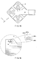
- FIG. 15 is a plan view showing a state where the lead wire 182 is arranged at a predetermined position on the strain body 16 shown in FIG. 13 by the anisotropic conductive film 181.
- FIG. 16 is an enlarged plan view showing a portion surrounded by a broken line in FIG. 15 .
- a plurality of terminals included in the electrode 171 and the ends of a plurality of wires included in the lead wire 182 are aligned in a state where the anisotropic conductive film 181 is stuck on the electrode 171.
- positioning is performed with an alignment mark AM16 provided on the strain body 16 and an alignment mark AMF provided on the lead wire 182 at a predetermined position, in this process.
- the position of the lead wire 182 is determined such that, for example, the positions of alignment marks AM16a and AM16b of the strain body 16 represented by a broken line and positions of alignment marks AMFa and AMFb of the lead wire 182 represented by the solid line have a relationship shown and enlarged in FIG. 16 .
- the alignment is performed such that one protruding portion of the alignment mark AMFa of the lead wire 182 is sandwiched between two protruding portions of the alignment mark AM16a of the strain body 16, and displacement in the longitudinal direction of the paper surface can be thereby prevented.
- displacement in the lateral direction of the paper surface can be prevented by performing the alignment such that the alignment mark AM16b of the strain body 16 and the alignment mark AMFb of the lead wire 182 overlap (ST2).
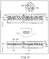
- FIG. 17 is a cross-sectional view for schematically illustrating electrically connecting between a plurality of terminals (PADs) 171a included in the electrode 171 and a plurality of wire terminals (PADs) 182a included in the lead wire 182 by using the anisotropic conductive film 181.
- the anisotropic conductive film 181 has a structure in which conductive particles 181a serving as a conductor are dispersed almost uniformly in a thermoset resin 181b serving as an insulator.
- the electrode 171 serving as a stacked body, the anisotropic conductive film 181, and lead wire 182 are pressurized while being heated, by a head 200 from above the lead wire 182, in a state in which terminals 171a of the electrode 171 and terminals 182a of the lead wire 182 are aligned.
- the conductive particles 181a in the anisotropic conductive film 181 are connected to each other by pressure, at positions Aa sandwiched by the terminals 171a and the terminals 182a, and a conductive path is formed to electrically connect the terminals 171a and the terminals 182a in the longitudinal direction (Z-axis direction) in the drawing.
- the pressure to the anisotropic conductive film 181 at positions Ab is lower than that at the positions Aa, the conductive particles 181a in the anisotropic conductive film 181 are not connected to each other and the insulating property is maintained.
- a conductive path in the longitudinal direction (Z-axis direction) in the drawing is formed only at the positions Aa sandwiched between the terminals 171a and the terminals 182a (ST3).
- the strain body 16 according to the third embodiment can electrically connect the terminals 171a of the electrode 171 and the terminals 182a of the lead wire 182, which is an FPC, to each other, by using the anisotropic conductive film 181 ( FIG. 14 to FIG. 17 ).
- a plurality of terminals 171a of the electrode 171 and a plurality of terminals 182a of the lead wire 182 can be connected at one time, by collecting the wire 172 to the central portion 161 and using the anisotropic conductive film 181. Therefore, the conductivity and the insulation can be maintained together in a few manufacturing processes, and the manufacturing costs can be reduced.
- connection using the anisotropic conductive film 181 enables reduction in weight and thinning as compared with connection using solder and connectors and the like, the mounting space can be reduced.
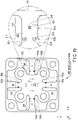
- FIG. 18 shows an example of connection between the strain body 16 and the lead wire 182 using the anisotropic conductive films ACF1 to ACF3 of the same type.
- the resistance value is almost constant regardless of the position of the pad, in any of the three anisotropic conductive films ACF1 to ACF3, a reliable electrical connection is understood to be secured.
- the resistance value approximately 0.1 ⁇ , of the terminals 182a of the lead wire 182 is subtracted from the resistance values shown in FIG.
- the substantial resistance values of the three anisotropic conductive films ACF1 to ACF3 are approximately 0.35 ⁇ to 0.45 ⁇ .
- the resistance values are values sufficiently lower than a reference value of a resistance value of a general anisotropic conductive film.
- the force sensor 10 restricts the range of operation of the movable body 12, and comprises the stoppers 14 comprising the first side surfaces 14a, which can contact the inner surfaces of the opening portions 13, on their outermost peripheral portions.
- the stoppers 14 have a simple shape, and have a protective function for all the six-axis directions.
- the force sensor 10 which is highly sensitive and has an advantage in reducing a manufacturing cost, can be provided.
- FIG. 19 is a plan view showing an overall structure of the strain body according to the fourth embodiment as viewed from its main surface side.
- the strain body 16B As shown and enlarged in FIG. 19 , in the strain body 16B according to the fourth embodiment, eight second strain sensors S1, S2, S15, S16, S17, S18, S25, and S26 provided in the second connecting portion 163b are arranged to have a sufficient distance LS from the groove GR to the same extent as the other second strain sensors.
- the strain body is different from the strain body 16A of the second embodiment with respect to this point.
- FIG. 19 shows the second strain sensors S17 and S18 alone. For this reason, all the second strain sensors provided in the second connecting portion 163b are not affected by the strain increasing effect from the groove GR.
- the distance LS is desirably set such that the strain amount of the first strain sensor provided in the first connecting portion 163a is understood to be distinctly different by, for example, 50% from the strain amount of the second strain sensor provided in the second connecting portion 163b.
- восем ⁇ second strain sensors S1, S2, S15, S16, S17, S18, S25, and S26 provided in the second connecting portion 163b are arranged to have a sufficient distance LS from the grooves GR to approximately the same extent as the other second strain sensors ( FIG. 19 ).
- the second strain sensor provided in the second connecting portion 163b is not affected by the strain increase effect from the groove GR, and the strain amounts of the first strain sensors S3, S5, S11, S13, S19, S21, S27, and S29 provided in the first connecting portion 163a can be increased as compared with the strain amounts of the second strain sensor S1, S2, S7, S8, S9, S10, S15, S16, S17, S18, S23, S24, S25, S26, S31, and S32 provided in the second connecting portion 163b.
- the detection accuracy of the four bridge circuits BF2, BF4, BF6, and BF8 can be improved.
- the embodiment is advantageous with respect to the feature that the strain amount of the second strain sensors can be made uniform.
- first to fourth embodiments have been described as examples, the embodiments of the present invention are not limited to the above-described first to fourth embodiments, and can be modified in various ways as necessary as a matter of course.
- strain bodies 16, 16A, and 16B are not limited to the force sensor 10 described in the third embodiment, and they can be applied to various types of sensor as a matter of course.
- the force sensor according to the embodiments of the present invention can be applied to, for example, joints of robot arms, and the like.
- 10 force sensor, 11 ... main body, 12 ... movable body, 14 ... stopper, 16, 16A, 16B ... strain body, 161 ... central portion, 162 ... outer peripheral portion, 163 ... connecting portion (beam portion), 161a ... first connecting portion, 161b ... second connecting portion, 171 ... electrode, 172 ... wire, 181 ... anisotropic conductive film (ACF), 182 ... lead wire, S1 to S32 ... strain sensor, RS4 to RS30 ... reference resistor, BF1, BF3, BF5, BF7 ... full bridge circuit, BF2, BF4, BF6, BF8 ... bridge circuit, GR ... strain increasing portion.
- ACF anisotropic conductive film
Landscapes
- Physics & Mathematics (AREA)
- General Physics & Mathematics (AREA)
- Engineering & Computer Science (AREA)
- Human Computer Interaction (AREA)
- Robotics (AREA)
- Mechanical Engineering (AREA)
- Force Measurement Appropriate To Specific Purposes (AREA)
- Measurement Of Force In General (AREA)
Claims (7)
- Belastungskörper, aufweisend:einen zentralen Bereich (161);einen äußeren Umfangsbereich (162), der den zentralen Bereich (161) umgibt;Verbindungsbereiche (163), die den zentralen Bereich (161) und den äußeren Umfangsbereich (162) verbinden;Belastungssensoren (S1 - S32), die auf Hauptflächen der Verbindungsbereiche (163) vorgesehen sind;Referenzwiderstände (RS4 - RS30), die auf einer Hauptfläche des zentralen Bereichs (161) vorgesehen sind und eine Brückenschaltung (BF2, BF4, BF6, BF8) mit den Belastungssensoren bilden;eine Elektrode (171), die auf einer Hauptfläche des zentralen Bereichs (161) vorgesehen und elektrisch an die Belastungssensoren (S1 - S32) und die Referenzwiderstände (RS4 - RS30) angeschlossen ist, um ein Erfassungssignal der Brückenschaltung aufzunehmen;einen Anschlussdraht (182), der eine elektrische Verbindung zwischen der Elektrode (171) und der Außenseite herstellt;einen anisotropen leitfähigen Film (181), der zwischen der Elektrode (171) und dem Anschlussdraht (182) vorgesehen ist, um eine elektrische Verbindung zwischen einem Anschluss der Elektrode (171) und einem Anschluss des Anschlussdrahts (182) herzustellen; undeinen Draht (172), der auf Hauptflächen des zentralen Bereichs und des Verbindungsbereichs vorgesehen ist, um die Belastungssensoren (S1 - S32), die Referenzwiderstände (RS4 - RS30) und die Elektrode (171) elektrisch zu verbinden,wobeidie Belastungssensoren (S1 - S32), die Referenzwiderstände (RS4 - RS30), die Elektrode (171) und der Draht (172) symmetrisch auf beiden Seiten von diagonalen Linien (L1) angeordnet sind, die Eckabschnitte des äußeren Umfangsbereichs (162) verbinden.
- Belastungskörper nach Anspruch 1, wobeijeder der Verbindungsbereiche (163) einen ersten Verbindungsbereich (161a) angrenzend an den äußeren Umfangsbereich (162) und einen zweiten Verbindungsbereich (161b) angrenzend an den zentralen Bereich (161) aufweist, undder erste Verbindungsbereich (161a) einen Belastungserhöhungsbereich (GR) enthält, der eine größere Belastung generiert als die Belastung, die im zweiten Verbindungsbereich (161b) generiert wird, wobei der Belastungserhöhungsbereich (GR) eine Nut aufweist, die in einer Dickenrichtung des Belastungsungskörpers ausgespart ist.
- Belastungskörper nach Anspruch 2, wobei
mindestens einer der Belastungssensoren die Brückenschaltung (BF2, BF4, BF6, BF8) auf einer Hauptfläche des ersten Verbindungsbereichs (161a) bildet. - Belastungskörper nach Anspruch 2, wobei
die Belastungssensoren eine volle Brückenschaltung (BF1, BF3, BF5, BF7) auf einer Hauptfläche des zweiten Verbindungsbereichs (161b) bilden. - Belastungskörper nach Anspruch 1, wobei
eine Elastizität des äußeren Umfangsbereichs (162) und des Verbindungsbereichs (163) größer ist als eine Elastizität des zentralen Bereichs. - Kraftsensor, aufweisend:den Belastungskörper nach einem der Ansprüche 1 bis 5;einen zylindrischen Hauptkörper (11); undeinen zylindrischen, beweglichen Körper (12), der in der Lage ist, den Hauptkörper (11) zu betätigen,wobeider zentrale Bereich (161) des Belastungskörpers mit dem Hauptkörper (11) oder dem beweglichen Körper (12) verbunden ist, undder äußere Umfangsbereich (162) des Belastungskörpers mit dem jeweils anderen des Hauptkörpers (161) oder beweglichen Körpers (12) verbunden ist.
- Kraftsensor nach Anspruch 6, darüber hinaus aufweisend:zumindest drei kreisförmige Öffnungsbereiche (13), die in der Umgebung des beweglichen Körpers (12) vorgesehen sind;Anschläge (14), die innerhalb der jeweiligen Öffnungsbereiche (13) angeordnet sind und jeweils eine erste Seitenfläche mit einem ersten Außendurchmesser aufweisen, der kleiner ist als ein Durchmesser jedes der Öffnungsbereiche (13); undBefestigungsteile, welche die Anschläge (14) am Hauptkörper befestigen.
Applications Claiming Priority (2)
| Application Number | Priority Date | Filing Date | Title |
|---|---|---|---|
| JP2017033447A JP6794293B2 (ja) | 2017-02-24 | 2017-02-24 | 起歪体およびその起歪体を備えた力覚センサ |
| PCT/JP2017/045159 WO2018154935A1 (ja) | 2017-02-24 | 2017-12-15 | 起歪体およびその起歪体を備えた力覚センサ |
Publications (3)
| Publication Number | Publication Date |
|---|---|
| EP3588040A1 EP3588040A1 (de) | 2020-01-01 |
| EP3588040A4 EP3588040A4 (de) | 2021-01-06 |
| EP3588040B1 true EP3588040B1 (de) | 2022-11-23 |
Family
ID=63253333
Family Applications (1)
| Application Number | Title | Priority Date | Filing Date |
|---|---|---|---|
| EP17897602.3A Not-in-force EP3588040B1 (de) | 2017-02-24 | 2017-12-15 | Dehnelement und kraftsensor mit dehnelement |
Country Status (5)
| Country | Link |
|---|---|
| US (1) | US11187598B2 (de) |
| EP (1) | EP3588040B1 (de) |
| JP (1) | JP6794293B2 (de) |
| CN (1) | CN110325832A (de) |
| WO (1) | WO2018154935A1 (de) |
Families Citing this family (7)
| Publication number | Priority date | Publication date | Assignee | Title |
|---|---|---|---|---|
| JP7426794B2 (ja) * | 2019-10-01 | 2024-02-02 | ミネベアミツミ株式会社 | センサモジュール |
| CN115280122B (zh) * | 2020-03-19 | 2026-04-17 | 导科国际贸易有限公司 | 扭矩传感器及机器人关节结构 |
| US11846557B2 (en) * | 2020-05-29 | 2023-12-19 | Bota Systems AG | Torque and force transducer |
| CN118786010A (zh) * | 2022-01-25 | 2024-10-15 | 卡莫齐自动化股份公司 | 用于夹持器的传感器式指状件 |
| CN115773833A (zh) * | 2022-12-09 | 2023-03-10 | 武汉飞恩微电子有限公司 | 一种力传感器 |
| CN115931188A (zh) * | 2022-12-09 | 2023-04-07 | 武汉飞恩微电子有限公司 | 一种力传感器 |
| CN121141015B (zh) * | 2025-11-14 | 2026-02-24 | 常州坤维传感科技有限公司 | 一种微型六维力传感器、冗余输出方法及机器人灵巧手 |
Family Cites Families (28)
| Publication number | Priority date | Publication date | Assignee | Title |
|---|---|---|---|---|
| JPH0643937B2 (ja) * | 1987-09-11 | 1994-06-08 | 日立建機株式会社 | 荷重検出装置 |
| US5081867A (en) * | 1988-09-30 | 1992-01-21 | Nec Corporation | Semiconductor sensor |
| EP1059517A4 (de) * | 1998-12-24 | 2002-03-06 | Mitsubishi Electric Corp | Drucksensor |
| WO2003031907A1 (en) * | 2001-10-02 | 2003-04-17 | Matsushita Electric Industrial Co., Ltd. | Strain sensor and method of producing the same |
| US6871552B2 (en) * | 2002-04-12 | 2005-03-29 | Deutsches Zentrum für Luft- und Raumfahrt e.V. | Force moment sensor |
| JP3969228B2 (ja) * | 2002-07-19 | 2007-09-05 | 松下電工株式会社 | 機械的変形量検出センサ及びそれを用いた加速度センサ、圧力センサ |
| JP2004239621A (ja) * | 2003-02-03 | 2004-08-26 | Japan Science & Technology Agency | 3次元圧力センサ |
| US6886415B1 (en) * | 2004-08-03 | 2005-05-03 | Toshiba Electric Engineering Corporation | Tactile sensor and gripping robot using the same |
| JP4779333B2 (ja) * | 2004-10-05 | 2011-09-28 | パナソニック株式会社 | 歪検出装置 |
| FR2883372B1 (fr) * | 2005-03-17 | 2007-06-29 | Commissariat Energie Atomique | Dispositif de mesure de force par detection resistive a double pont de wheastone |
| JP4203051B2 (ja) | 2005-06-28 | 2008-12-24 | 本田技研工業株式会社 | 力覚センサ |
| JP5303101B2 (ja) | 2006-05-02 | 2013-10-02 | 本田技研工業株式会社 | 力覚センサ用チップ |
| JP5248221B2 (ja) * | 2008-06-30 | 2013-07-31 | 株式会社ワコー | 力覚センサおよびその組立方法 |
| CN102317750B (zh) | 2009-02-06 | 2015-07-22 | Abb股份公司 | 多轴线力和扭矩传感器的组及组装方法 |
| CN101625978A (zh) * | 2009-08-07 | 2010-01-13 | 广东中显科技有限公司 | 平板显示器电气元件绑定生产工艺 |
| JP2011112419A (ja) * | 2009-11-25 | 2011-06-09 | Alps Electric Co Ltd | フォースセンサ及びその実装方法 |
| JP5572001B2 (ja) * | 2010-04-23 | 2014-08-13 | 本田技研工業株式会社 | 物理量センサ |
| US8421311B2 (en) * | 2010-04-30 | 2013-04-16 | Southern Taiwan University Of Technology | Flexible piezoelectric tactile sensor |
| JP5817371B2 (ja) | 2011-09-15 | 2015-11-18 | トヨタ自動車株式会社 | トルク計測装置 |
| CN102589765B (zh) * | 2012-03-19 | 2014-07-23 | 南宁宇立汽车安全技术研发有限公司 | 多维力传感器 |
| DE102012210021A1 (de) * | 2012-06-14 | 2013-12-19 | Tecsis Gmbh | Kraftsensor mit einer Sensorplatte mit lokalen Unterschieden der Steifigkeit |
| JP2015029209A (ja) | 2013-07-30 | 2015-02-12 | 株式会社東芝 | 受信装置、送信装置、及び送受信システム |
| JP6135408B2 (ja) | 2013-09-04 | 2017-05-31 | トヨタ自動車株式会社 | トルクセンサ、駆動装置、及びロボット |
| KR102302811B1 (ko) * | 2013-12-16 | 2021-09-16 | 엘지이노텍 주식회사 | 터치 패널 |
| JP6869710B2 (ja) * | 2016-12-09 | 2021-05-12 | 日本電産コパル電子株式会社 | 起歪体およびその起歪体を備えた力覚センサ |
| JP6776152B2 (ja) * | 2017-02-24 | 2020-10-28 | 日本電産コパル電子株式会社 | 起歪体およびその起歪体を備えた力覚センサ |
| JP6776151B2 (ja) * | 2017-02-24 | 2020-10-28 | 日本電産コパル電子株式会社 | 起歪体およびその起歪体を備えた力覚センサ |
| JP6469927B1 (ja) * | 2018-10-23 | 2019-02-13 | 株式会社浅沼技研 | 検査マスタ |
-
2017
- 2017-02-24 JP JP2017033447A patent/JP6794293B2/ja active Active
- 2017-12-15 EP EP17897602.3A patent/EP3588040B1/de not_active Not-in-force
- 2017-12-15 WO PCT/JP2017/045159 patent/WO2018154935A1/ja not_active Ceased
- 2017-12-15 CN CN201780087153.6A patent/CN110325832A/zh active Pending
-
2019
- 2019-08-23 US US16/549,231 patent/US11187598B2/en active Active
Also Published As
| Publication number | Publication date |
|---|---|
| EP3588040A1 (de) | 2020-01-01 |
| JP6794293B2 (ja) | 2020-12-02 |
| EP3588040A4 (de) | 2021-01-06 |
| CN110325832A (zh) | 2019-10-11 |
| JP2018138890A (ja) | 2018-09-06 |
| US11187598B2 (en) | 2021-11-30 |
| WO2018154935A1 (ja) | 2018-08-30 |
| US20190376857A1 (en) | 2019-12-12 |
Similar Documents
| Publication | Publication Date | Title |
|---|---|---|
| EP3588041B1 (de) | Elastischer körper und kraftsensor mit dem elastischen körper | |
| EP3588040B1 (de) | Dehnelement und kraftsensor mit dehnelement | |
| US11085842B2 (en) | Strain generation body and force sensor equipped with strain generation body | |
| US20190376855A1 (en) | Strain body and force sensor provided with the strain body | |
| US20090007696A1 (en) | Strain gauge type sensor | |
| US7353713B2 (en) | Flexible apparatus and method to enhance capacitive force sensing | |
| JP6611761B2 (ja) | ひずみゲージ及び多軸力センサ | |
| JP7073471B2 (ja) | 起歪体 | |
| US11895776B2 (en) | Flexible printed wiring board, joined body, pressure sensor and mass flow controller | |
| JP5174793B2 (ja) | フレキシブルプリント基板 | |
| WO2021125014A1 (ja) | フォースセンサ | |
| JPS6321531A (ja) | 力検出装置 | |
| JP6837113B2 (ja) | ひずみゲージ及び多軸力センサ | |
| JP2024065855A (ja) | 触覚センサ | |
| WO2026088518A1 (ja) | トルクセンサ | |
| WO2025197255A1 (ja) | せん断力センサー | |
| JP2024065854A (ja) | 触覚センサ | |
| CN117629469A (zh) | 压力传感器模组及其制作方法 | |
| WO2022163324A1 (ja) | 歪みセンサ | |
| CN120825871A (zh) | 感压电路板及其制备方法、柔性感压元件 | |
| JPH04177102A (ja) | 変換器用ひずみゲージ |
Legal Events
| Date | Code | Title | Description |
|---|---|---|---|
| STAA | Information on the status of an ep patent application or granted ep patent |
Free format text: STATUS: THE INTERNATIONAL PUBLICATION HAS BEEN MADE |
|
| PUAI | Public reference made under article 153(3) epc to a published international application that has entered the european phase |
Free format text: ORIGINAL CODE: 0009012 |
|
| STAA | Information on the status of an ep patent application or granted ep patent |
Free format text: STATUS: REQUEST FOR EXAMINATION WAS MADE |
|
| 17P | Request for examination filed |
Effective date: 20190918 |
|
| AK | Designated contracting states |
Kind code of ref document: A1 Designated state(s): AL AT BE BG CH CY CZ DE DK EE ES FI FR GB GR HR HU IE IS IT LI LT LU LV MC MK MT NL NO PL PT RO RS SE SI SK SM TR |
|
| AX | Request for extension of the european patent |
Extension state: BA ME |
|
| DAV | Request for validation of the european patent (deleted) | ||
| DAX | Request for extension of the european patent (deleted) | ||
| A4 | Supplementary search report drawn up and despatched |
Effective date: 20201203 |
|
| RIC1 | Information provided on ipc code assigned before grant |
Ipc: B25J 13/08 20060101ALI20201127BHEP Ipc: G01L 1/22 20060101ALI20201127BHEP Ipc: G01L 5/161 20200101ALI20201127BHEP Ipc: G01L 5/16 20200101AFI20201127BHEP Ipc: G01L 5/162 20200101ALI20201127BHEP |
|
| REG | Reference to a national code |
Ref country code: DE Ref legal event code: R079 Ref document number: 602017064032 Country of ref document: DE Free format text: PREVIOUS MAIN CLASS: G01L0005160000 Ipc: G01L0005162700 |
|
| GRAP | Despatch of communication of intention to grant a patent |
Free format text: ORIGINAL CODE: EPIDOSNIGR1 |
|
| STAA | Information on the status of an ep patent application or granted ep patent |
Free format text: STATUS: GRANT OF PATENT IS INTENDED |
|
| RIC1 | Information provided on ipc code assigned before grant |
Ipc: B25J 13/08 20060101ALI20220523BHEP Ipc: G01L 1/22 20060101ALI20220523BHEP Ipc: G01L 5/1627 20200101AFI20220523BHEP |
|
| INTG | Intention to grant announced |
Effective date: 20220614 |
|
| GRAS | Grant fee paid |
Free format text: ORIGINAL CODE: EPIDOSNIGR3 |
|
| GRAA | (expected) grant |
Free format text: ORIGINAL CODE: 0009210 |
|
| STAA | Information on the status of an ep patent application or granted ep patent |
Free format text: STATUS: THE PATENT HAS BEEN GRANTED |
|
| AK | Designated contracting states |
Kind code of ref document: B1 Designated state(s): AL AT BE BG CH CY CZ DE DK EE ES FI FR GB GR HR HU IE IS IT LI LT LU LV MC MK MT NL NO PL PT RO RS SE SI SK SM TR |
|
| REG | Reference to a national code |
Ref country code: GB Ref legal event code: FG4D |
|
| REG | Reference to a national code |
Ref country code: CH Ref legal event code: EP |
|
| REG | Reference to a national code |
Ref country code: AT Ref legal event code: REF Ref document number: 1533406 Country of ref document: AT Kind code of ref document: T Effective date: 20221215 Ref country code: DE Ref legal event code: R096 Ref document number: 602017064032 Country of ref document: DE |
|
| REG | Reference to a national code |
Ref country code: IE Ref legal event code: FG4D |
|
| REG | Reference to a national code |
Ref country code: LT Ref legal event code: MG9D |
|
| REG | Reference to a national code |
Ref country code: NL Ref legal event code: MP Effective date: 20221123 |
|
| REG | Reference to a national code |
Ref country code: AT Ref legal event code: MK05 Ref document number: 1533406 Country of ref document: AT Kind code of ref document: T Effective date: 20221123 |
|
| PG25 | Lapsed in a contracting state [announced via postgrant information from national office to epo] |
Ref country code: SE Free format text: LAPSE BECAUSE OF FAILURE TO SUBMIT A TRANSLATION OF THE DESCRIPTION OR TO PAY THE FEE WITHIN THE PRESCRIBED TIME-LIMIT Effective date: 20221123 Ref country code: PT Free format text: LAPSE BECAUSE OF FAILURE TO SUBMIT A TRANSLATION OF THE DESCRIPTION OR TO PAY THE FEE WITHIN THE PRESCRIBED TIME-LIMIT Effective date: 20230323 Ref country code: NO Free format text: LAPSE BECAUSE OF FAILURE TO SUBMIT A TRANSLATION OF THE DESCRIPTION OR TO PAY THE FEE WITHIN THE PRESCRIBED TIME-LIMIT Effective date: 20230223 Ref country code: LT Free format text: LAPSE BECAUSE OF FAILURE TO SUBMIT A TRANSLATION OF THE DESCRIPTION OR TO PAY THE FEE WITHIN THE PRESCRIBED TIME-LIMIT Effective date: 20221123 Ref country code: FI Free format text: LAPSE BECAUSE OF FAILURE TO SUBMIT A TRANSLATION OF THE DESCRIPTION OR TO PAY THE FEE WITHIN THE PRESCRIBED TIME-LIMIT Effective date: 20221123 Ref country code: ES Free format text: LAPSE BECAUSE OF FAILURE TO SUBMIT A TRANSLATION OF THE DESCRIPTION OR TO PAY THE FEE WITHIN THE PRESCRIBED TIME-LIMIT Effective date: 20221123 Ref country code: AT Free format text: LAPSE BECAUSE OF FAILURE TO SUBMIT A TRANSLATION OF THE DESCRIPTION OR TO PAY THE FEE WITHIN THE PRESCRIBED TIME-LIMIT Effective date: 20221123 |
|
| PG25 | Lapsed in a contracting state [announced via postgrant information from national office to epo] |
Ref country code: RS Free format text: LAPSE BECAUSE OF FAILURE TO SUBMIT A TRANSLATION OF THE DESCRIPTION OR TO PAY THE FEE WITHIN THE PRESCRIBED TIME-LIMIT Effective date: 20221123 Ref country code: PL Free format text: LAPSE BECAUSE OF FAILURE TO SUBMIT A TRANSLATION OF THE DESCRIPTION OR TO PAY THE FEE WITHIN THE PRESCRIBED TIME-LIMIT Effective date: 20221123 Ref country code: LV Free format text: LAPSE BECAUSE OF FAILURE TO SUBMIT A TRANSLATION OF THE DESCRIPTION OR TO PAY THE FEE WITHIN THE PRESCRIBED TIME-LIMIT Effective date: 20221123 Ref country code: IS Free format text: LAPSE BECAUSE OF FAILURE TO SUBMIT A TRANSLATION OF THE DESCRIPTION OR TO PAY THE FEE WITHIN THE PRESCRIBED TIME-LIMIT Effective date: 20230323 Ref country code: HR Free format text: LAPSE BECAUSE OF FAILURE TO SUBMIT A TRANSLATION OF THE DESCRIPTION OR TO PAY THE FEE WITHIN THE PRESCRIBED TIME-LIMIT Effective date: 20221123 Ref country code: GR Free format text: LAPSE BECAUSE OF FAILURE TO SUBMIT A TRANSLATION OF THE DESCRIPTION OR TO PAY THE FEE WITHIN THE PRESCRIBED TIME-LIMIT Effective date: 20230224 |
|
| PG25 | Lapsed in a contracting state [announced via postgrant information from national office to epo] |
Ref country code: NL Free format text: LAPSE BECAUSE OF FAILURE TO SUBMIT A TRANSLATION OF THE DESCRIPTION OR TO PAY THE FEE WITHIN THE PRESCRIBED TIME-LIMIT Effective date: 20221123 |
|
| PG25 | Lapsed in a contracting state [announced via postgrant information from national office to epo] |
Ref country code: SM Free format text: LAPSE BECAUSE OF FAILURE TO SUBMIT A TRANSLATION OF THE DESCRIPTION OR TO PAY THE FEE WITHIN THE PRESCRIBED TIME-LIMIT Effective date: 20221123 Ref country code: RO Free format text: LAPSE BECAUSE OF FAILURE TO SUBMIT A TRANSLATION OF THE DESCRIPTION OR TO PAY THE FEE WITHIN THE PRESCRIBED TIME-LIMIT Effective date: 20221123 Ref country code: EE Free format text: LAPSE BECAUSE OF FAILURE TO SUBMIT A TRANSLATION OF THE DESCRIPTION OR TO PAY THE FEE WITHIN THE PRESCRIBED TIME-LIMIT Effective date: 20221123 Ref country code: DK Free format text: LAPSE BECAUSE OF FAILURE TO SUBMIT A TRANSLATION OF THE DESCRIPTION OR TO PAY THE FEE WITHIN THE PRESCRIBED TIME-LIMIT Effective date: 20221123 Ref country code: CZ Free format text: LAPSE BECAUSE OF FAILURE TO SUBMIT A TRANSLATION OF THE DESCRIPTION OR TO PAY THE FEE WITHIN THE PRESCRIBED TIME-LIMIT Effective date: 20221123 |
|
| REG | Reference to a national code |
Ref country code: CH Ref legal event code: PL |
|
| REG | Reference to a national code |
Ref country code: DE Ref legal event code: R097 Ref document number: 602017064032 Country of ref document: DE Ref country code: BE Ref legal event code: MM Effective date: 20221231 |
|
| PG25 | Lapsed in a contracting state [announced via postgrant information from national office to epo] |
Ref country code: SK Free format text: LAPSE BECAUSE OF FAILURE TO SUBMIT A TRANSLATION OF THE DESCRIPTION OR TO PAY THE FEE WITHIN THE PRESCRIBED TIME-LIMIT Effective date: 20221123 Ref country code: LU Free format text: LAPSE BECAUSE OF NON-PAYMENT OF DUE FEES Effective date: 20221215 Ref country code: AL Free format text: LAPSE BECAUSE OF FAILURE TO SUBMIT A TRANSLATION OF THE DESCRIPTION OR TO PAY THE FEE WITHIN THE PRESCRIBED TIME-LIMIT Effective date: 20221123 |
|
| PLBE | No opposition filed within time limit |
Free format text: ORIGINAL CODE: 0009261 |
|
| STAA | Information on the status of an ep patent application or granted ep patent |
Free format text: STATUS: NO OPPOSITION FILED WITHIN TIME LIMIT |
|
| GBPC | Gb: european patent ceased through non-payment of renewal fee |
Effective date: 20230223 |
|
| PG25 | Lapsed in a contracting state [announced via postgrant information from national office to epo] |
Ref country code: LI Free format text: LAPSE BECAUSE OF NON-PAYMENT OF DUE FEES Effective date: 20221231 Ref country code: IE Free format text: LAPSE BECAUSE OF NON-PAYMENT OF DUE FEES Effective date: 20221215 Ref country code: CH Free format text: LAPSE BECAUSE OF NON-PAYMENT OF DUE FEES Effective date: 20221231 |
|
| 26N | No opposition filed |
Effective date: 20230824 |
|
| PG25 | Lapsed in a contracting state [announced via postgrant information from national office to epo] |
Ref country code: SI Free format text: LAPSE BECAUSE OF FAILURE TO SUBMIT A TRANSLATION OF THE DESCRIPTION OR TO PAY THE FEE WITHIN THE PRESCRIBED TIME-LIMIT Effective date: 20221123 Ref country code: FR Free format text: LAPSE BECAUSE OF NON-PAYMENT OF DUE FEES Effective date: 20230123 Ref country code: BE Free format text: LAPSE BECAUSE OF NON-PAYMENT OF DUE FEES Effective date: 20221231 |
|
| PG25 | Lapsed in a contracting state [announced via postgrant information from national office to epo] |
Ref country code: GB Free format text: LAPSE BECAUSE OF NON-PAYMENT OF DUE FEES Effective date: 20230223 |
|
| PG25 | Lapsed in a contracting state [announced via postgrant information from national office to epo] |
Ref country code: GB Free format text: LAPSE BECAUSE OF NON-PAYMENT OF DUE FEES Effective date: 20230223 |
|
| PGFP | Annual fee paid to national office [announced via postgrant information from national office to epo] |
Ref country code: DE Payment date: 20231031 Year of fee payment: 7 |
|
| PG25 | Lapsed in a contracting state [announced via postgrant information from national office to epo] |
Ref country code: HU Free format text: LAPSE BECAUSE OF FAILURE TO SUBMIT A TRANSLATION OF THE DESCRIPTION OR TO PAY THE FEE WITHIN THE PRESCRIBED TIME-LIMIT; INVALID AB INITIO Effective date: 20171215 |
|
| PG25 | Lapsed in a contracting state [announced via postgrant information from national office to epo] |
Ref country code: CY Free format text: LAPSE BECAUSE OF FAILURE TO SUBMIT A TRANSLATION OF THE DESCRIPTION OR TO PAY THE FEE WITHIN THE PRESCRIBED TIME-LIMIT Effective date: 20221123 |
|
| PG25 | Lapsed in a contracting state [announced via postgrant information from national office to epo] |
Ref country code: MK Free format text: LAPSE BECAUSE OF FAILURE TO SUBMIT A TRANSLATION OF THE DESCRIPTION OR TO PAY THE FEE WITHIN THE PRESCRIBED TIME-LIMIT Effective date: 20221123 Ref country code: IT Free format text: LAPSE BECAUSE OF FAILURE TO SUBMIT A TRANSLATION OF THE DESCRIPTION OR TO PAY THE FEE WITHIN THE PRESCRIBED TIME-LIMIT Effective date: 20221123 |
|
| PG25 | Lapsed in a contracting state [announced via postgrant information from national office to epo] |
Ref country code: MC Free format text: LAPSE BECAUSE OF FAILURE TO SUBMIT A TRANSLATION OF THE DESCRIPTION OR TO PAY THE FEE WITHIN THE PRESCRIBED TIME-LIMIT Effective date: 20221123 |
|
| PG25 | Lapsed in a contracting state [announced via postgrant information from national office to epo] |
Ref country code: TR Free format text: LAPSE BECAUSE OF FAILURE TO SUBMIT A TRANSLATION OF THE DESCRIPTION OR TO PAY THE FEE WITHIN THE PRESCRIBED TIME-LIMIT Effective date: 20221123 Ref country code: MC Free format text: LAPSE BECAUSE OF FAILURE TO SUBMIT A TRANSLATION OF THE DESCRIPTION OR TO PAY THE FEE WITHIN THE PRESCRIBED TIME-LIMIT Effective date: 20221123 |
|
| PG25 | Lapsed in a contracting state [announced via postgrant information from national office to epo] |
Ref country code: BG Free format text: LAPSE BECAUSE OF FAILURE TO SUBMIT A TRANSLATION OF THE DESCRIPTION OR TO PAY THE FEE WITHIN THE PRESCRIBED TIME-LIMIT Effective date: 20221123 |
|
| PG25 | Lapsed in a contracting state [announced via postgrant information from national office to epo] |
Ref country code: MT Free format text: LAPSE BECAUSE OF FAILURE TO SUBMIT A TRANSLATION OF THE DESCRIPTION OR TO PAY THE FEE WITHIN THE PRESCRIBED TIME-LIMIT Effective date: 20221123 |
|
| REG | Reference to a national code |
Ref country code: DE Ref legal event code: R119 Ref document number: 602017064032 Country of ref document: DE |
|
| PG25 | Lapsed in a contracting state [announced via postgrant information from national office to epo] |
Ref country code: DE Free format text: LAPSE BECAUSE OF NON-PAYMENT OF DUE FEES Effective date: 20250701 |