EP3588151A1 - Lichtwellenlängenumwandlungselement und lichtemittierende vorrichtung - Google Patents
Lichtwellenlängenumwandlungselement und lichtemittierende vorrichtung Download PDFInfo
- Publication number
- EP3588151A1 EP3588151A1 EP17898117.1A EP17898117A EP3588151A1 EP 3588151 A1 EP3588151 A1 EP 3588151A1 EP 17898117 A EP17898117 A EP 17898117A EP 3588151 A1 EP3588151 A1 EP 3588151A1
- Authority
- EP
- European Patent Office
- Prior art keywords
- light
- wavelength conversion
- conversion member
- ceramic plate
- optical wavelength
- Prior art date
- Legal status (The legal status is an assumption and is not a legal conclusion. Google has not performed a legal analysis and makes no representation as to the accuracy of the status listed.)
- Withdrawn
Links
Images


Classifications
-
- G—PHYSICS
- G02—OPTICS
- G02B—OPTICAL ELEMENTS, SYSTEMS OR APPARATUS
- G02B5/00—Optical elements other than lenses
- G02B5/20—Filters
- G02B5/28—Interference filters
-
- C—CHEMISTRY; METALLURGY
- C09—DYES; PAINTS; POLISHES; NATURAL RESINS; ADHESIVES; COMPOSITIONS NOT OTHERWISE PROVIDED FOR; APPLICATIONS OF MATERIALS NOT OTHERWISE PROVIDED FOR
- C09K—MATERIALS FOR MISCELLANEOUS APPLICATIONS, NOT PROVIDED FOR ELSEWHERE
- C09K11/00—Luminescent materials, e.g. electroluminescent or chemiluminescent
- C09K11/08—Luminescent materials, e.g. electroluminescent or chemiluminescent containing inorganic luminescent materials
- C09K11/77—Luminescent materials, e.g. electroluminescent or chemiluminescent containing inorganic luminescent materials containing rare earth metals
- C09K11/7766—Luminescent materials, e.g. electroluminescent or chemiluminescent containing inorganic luminescent materials containing rare earth metals containing two or more rare earth metals
- C09K11/7774—Aluminates
-
- C—CHEMISTRY; METALLURGY
- C04—CEMENTS; CONCRETE; ARTIFICIAL STONE; CERAMICS; REFRACTORIES
- C04B—LIME, MAGNESIA; SLAG; CEMENTS; COMPOSITIONS THEREOF, e.g. MORTARS, CONCRETE OR LIKE BUILDING MATERIALS; ARTIFICIAL STONE; CERAMICS; REFRACTORIES; TREATMENT OF NATURAL STONE
- C04B35/00—Shaped ceramic products characterised by their composition; Ceramics compositions; Processing powders of inorganic compounds preparatory to the manufacturing of ceramic products
- C04B35/01—Shaped ceramic products characterised by their composition; Ceramics compositions; Processing powders of inorganic compounds preparatory to the manufacturing of ceramic products based on oxide ceramics
- C04B35/10—Shaped ceramic products characterised by their composition; Ceramics compositions; Processing powders of inorganic compounds preparatory to the manufacturing of ceramic products based on oxide ceramics based on aluminium oxide
- C04B35/111—Fine ceramics
- C04B35/115—Translucent or transparent products
-
- C—CHEMISTRY; METALLURGY
- C04—CEMENTS; CONCRETE; ARTIFICIAL STONE; CERAMICS; REFRACTORIES
- C04B—LIME, MAGNESIA; SLAG; CEMENTS; COMPOSITIONS THEREOF, e.g. MORTARS, CONCRETE OR LIKE BUILDING MATERIALS; ARTIFICIAL STONE; CERAMICS; REFRACTORIES; TREATMENT OF NATURAL STONE
- C04B35/00—Shaped ceramic products characterised by their composition; Ceramics compositions; Processing powders of inorganic compounds preparatory to the manufacturing of ceramic products
- C04B35/01—Shaped ceramic products characterised by their composition; Ceramics compositions; Processing powders of inorganic compounds preparatory to the manufacturing of ceramic products based on oxide ceramics
- C04B35/10—Shaped ceramic products characterised by their composition; Ceramics compositions; Processing powders of inorganic compounds preparatory to the manufacturing of ceramic products based on oxide ceramics based on aluminium oxide
- C04B35/111—Fine ceramics
- C04B35/117—Composites
-
- C—CHEMISTRY; METALLURGY
- C04—CEMENTS; CONCRETE; ARTIFICIAL STONE; CERAMICS; REFRACTORIES
- C04B—LIME, MAGNESIA; SLAG; CEMENTS; COMPOSITIONS THEREOF, e.g. MORTARS, CONCRETE OR LIKE BUILDING MATERIALS; ARTIFICIAL STONE; CERAMICS; REFRACTORIES; TREATMENT OF NATURAL STONE
- C04B41/00—After-treatment of mortars, concrete, artificial stone or ceramics; Treatment of natural stone
- C04B41/009—After-treatment of mortars, concrete, artificial stone or ceramics; Treatment of natural stone characterised by the material treated
-
- C—CHEMISTRY; METALLURGY
- C04—CEMENTS; CONCRETE; ARTIFICIAL STONE; CERAMICS; REFRACTORIES
- C04B—LIME, MAGNESIA; SLAG; CEMENTS; COMPOSITIONS THEREOF, e.g. MORTARS, CONCRETE OR LIKE BUILDING MATERIALS; ARTIFICIAL STONE; CERAMICS; REFRACTORIES; TREATMENT OF NATURAL STONE
- C04B41/00—After-treatment of mortars, concrete, artificial stone or ceramics; Treatment of natural stone
- C04B41/45—Coating or impregnating, e.g. injection in masonry, partial coating of green or fired ceramics, organic coating compositions for adhering together two concrete elements
- C04B41/52—Multiple coating or impregnating multiple coating or impregnating with the same composition or with compositions only differing in the concentration of the constituents, is classified as single coating or impregnation
-
- C—CHEMISTRY; METALLURGY
- C04—CEMENTS; CONCRETE; ARTIFICIAL STONE; CERAMICS; REFRACTORIES
- C04B—LIME, MAGNESIA; SLAG; CEMENTS; COMPOSITIONS THEREOF, e.g. MORTARS, CONCRETE OR LIKE BUILDING MATERIALS; ARTIFICIAL STONE; CERAMICS; REFRACTORIES; TREATMENT OF NATURAL STONE
- C04B41/00—After-treatment of mortars, concrete, artificial stone or ceramics; Treatment of natural stone
- C04B41/80—After-treatment of mortars, concrete, artificial stone or ceramics; Treatment of natural stone of only ceramics
- C04B41/81—Coating or impregnation
- C04B41/89—Coating or impregnation for obtaining at least two superposed coatings having different compositions
-
- C—CHEMISTRY; METALLURGY
- C09—DYES; PAINTS; POLISHES; NATURAL RESINS; ADHESIVES; COMPOSITIONS NOT OTHERWISE PROVIDED FOR; APPLICATIONS OF MATERIALS NOT OTHERWISE PROVIDED FOR
- C09K—MATERIALS FOR MISCELLANEOUS APPLICATIONS, NOT PROVIDED FOR ELSEWHERE
- C09K11/00—Luminescent materials, e.g. electroluminescent or chemiluminescent
- C09K11/02—Use of particular materials as binders, particle coatings or suspension media therefor
-
- C—CHEMISTRY; METALLURGY
- C09—DYES; PAINTS; POLISHES; NATURAL RESINS; ADHESIVES; COMPOSITIONS NOT OTHERWISE PROVIDED FOR; APPLICATIONS OF MATERIALS NOT OTHERWISE PROVIDED FOR
- C09K—MATERIALS FOR MISCELLANEOUS APPLICATIONS, NOT PROVIDED FOR ELSEWHERE
- C09K11/00—Luminescent materials, e.g. electroluminescent or chemiluminescent
- C09K11/08—Luminescent materials, e.g. electroluminescent or chemiluminescent containing inorganic luminescent materials
-
- F—MECHANICAL ENGINEERING; LIGHTING; HEATING; WEAPONS; BLASTING
- F21—LIGHTING
- F21V—FUNCTIONAL FEATURES OR DETAILS OF LIGHTING DEVICES OR SYSTEMS THEREOF; STRUCTURAL COMBINATIONS OF LIGHTING DEVICES WITH OTHER ARTICLES, NOT OTHERWISE PROVIDED FOR
- F21V9/00—Elements for modifying spectral properties, polarisation or intensity of the light emitted, e.g. filters
- F21V9/30—Elements containing photoluminescent material distinct from or spaced from the light source
-
- G—PHYSICS
- G02—OPTICS
- G02B—OPTICAL ELEMENTS, SYSTEMS OR APPARATUS
- G02B1/00—Optical elements characterised by the material of which they are made; Optical coatings for optical elements
- G02B1/10—Optical coatings produced by application to, or surface treatment of, optical elements
- G02B1/11—Anti-reflection coatings
-
- G—PHYSICS
- G02—OPTICS
- G02B—OPTICAL ELEMENTS, SYSTEMS OR APPARATUS
- G02B5/00—Optical elements other than lenses
- G02B5/20—Filters
- G02B5/28—Interference filters
- G02B5/285—Interference filters comprising deposited thin solid films
-
- H—ELECTRICITY
- H01—ELECTRIC ELEMENTS
- H01S—DEVICES USING THE PROCESS OF LIGHT AMPLIFICATION BY STIMULATED EMISSION OF RADIATION [LASER] TO AMPLIFY OR GENERATE LIGHT; DEVICES USING STIMULATED EMISSION OF ELECTROMAGNETIC RADIATION IN WAVE RANGES OTHER THAN OPTICAL
- H01S5/00—Semiconductor lasers
- H01S5/005—Optical components external to the laser cavity, specially adapted therefor, e.g. for homogenisation or merging of the beams or for manipulating laser pulses, e.g. pulse shaping
- H01S5/0087—Optical components external to the laser cavity, specially adapted therefor, e.g. for homogenisation or merging of the beams or for manipulating laser pulses, e.g. pulse shaping for illuminating phosphorescent or fluorescent materials, e.g. using optical arrangements specifically adapted for guiding or shaping laser beams illuminating these materials
-
- H—ELECTRICITY
- H01—ELECTRIC ELEMENTS
- H01S—DEVICES USING THE PROCESS OF LIGHT AMPLIFICATION BY STIMULATED EMISSION OF RADIATION [LASER] TO AMPLIFY OR GENERATE LIGHT; DEVICES USING STIMULATED EMISSION OF ELECTROMAGNETIC RADIATION IN WAVE RANGES OTHER THAN OPTICAL
- H01S5/00—Semiconductor lasers
- H01S5/02—Structural details or components not essential to laser action
-
- H—ELECTRICITY
- H10—SEMICONDUCTOR DEVICES; ELECTRIC SOLID-STATE DEVICES NOT OTHERWISE PROVIDED FOR
- H10H—INORGANIC LIGHT-EMITTING SEMICONDUCTOR DEVICES HAVING POTENTIAL BARRIERS
- H10H20/00—Individual inorganic light-emitting semiconductor devices having potential barriers, e.g. light-emitting diodes [LED]
- H10H20/80—Constructional details
- H10H20/85—Packages
- H10H20/851—Wavelength conversion means
-
- H—ELECTRICITY
- H10—SEMICONDUCTOR DEVICES; ELECTRIC SOLID-STATE DEVICES NOT OTHERWISE PROVIDED FOR
- H10H—INORGANIC LIGHT-EMITTING SEMICONDUCTOR DEVICES HAVING POTENTIAL BARRIERS
- H10H20/00—Individual inorganic light-emitting semiconductor devices having potential barriers, e.g. light-emitting diodes [LED]
- H10H20/80—Constructional details
- H10H20/85—Packages
- H10H20/851—Wavelength conversion means
- H10H20/8511—Wavelength conversion means characterised by their material, e.g. binder
- H10H20/8512—Wavelength conversion materials
-
- C—CHEMISTRY; METALLURGY
- C04—CEMENTS; CONCRETE; ARTIFICIAL STONE; CERAMICS; REFRACTORIES
- C04B—LIME, MAGNESIA; SLAG; CEMENTS; COMPOSITIONS THEREOF, e.g. MORTARS, CONCRETE OR LIKE BUILDING MATERIALS; ARTIFICIAL STONE; CERAMICS; REFRACTORIES; TREATMENT OF NATURAL STONE
- C04B2235/00—Aspects relating to ceramic starting mixtures or sintered ceramic products
- C04B2235/02—Composition of constituents of the starting material or of secondary phases of the final product
- C04B2235/30—Constituents and secondary phases not being of a fibrous nature
- C04B2235/32—Metal oxides, mixed metal oxides, or oxide-forming salts thereof, e.g. carbonates, nitrates, (oxy)hydroxides, chlorides
- C04B2235/3217—Aluminum oxide or oxide forming salts thereof, e.g. bauxite, alpha-alumina
- C04B2235/3222—Aluminates other than alumino-silicates, e.g. spinel (MgAl2O4)
-
- C—CHEMISTRY; METALLURGY
- C04—CEMENTS; CONCRETE; ARTIFICIAL STONE; CERAMICS; REFRACTORIES
- C04B—LIME, MAGNESIA; SLAG; CEMENTS; COMPOSITIONS THEREOF, e.g. MORTARS, CONCRETE OR LIKE BUILDING MATERIALS; ARTIFICIAL STONE; CERAMICS; REFRACTORIES; TREATMENT OF NATURAL STONE
- C04B2235/00—Aspects relating to ceramic starting mixtures or sintered ceramic products
- C04B2235/02—Composition of constituents of the starting material or of secondary phases of the final product
- C04B2235/30—Constituents and secondary phases not being of a fibrous nature
- C04B2235/32—Metal oxides, mixed metal oxides, or oxide-forming salts thereof, e.g. carbonates, nitrates, (oxy)hydroxides, chlorides
- C04B2235/3224—Rare earth oxide or oxide forming salts thereof, e.g. scandium oxide
-
- C—CHEMISTRY; METALLURGY
- C04—CEMENTS; CONCRETE; ARTIFICIAL STONE; CERAMICS; REFRACTORIES
- C04B—LIME, MAGNESIA; SLAG; CEMENTS; COMPOSITIONS THEREOF, e.g. MORTARS, CONCRETE OR LIKE BUILDING MATERIALS; ARTIFICIAL STONE; CERAMICS; REFRACTORIES; TREATMENT OF NATURAL STONE
- C04B2235/00—Aspects relating to ceramic starting mixtures or sintered ceramic products
- C04B2235/02—Composition of constituents of the starting material or of secondary phases of the final product
- C04B2235/30—Constituents and secondary phases not being of a fibrous nature
- C04B2235/32—Metal oxides, mixed metal oxides, or oxide-forming salts thereof, e.g. carbonates, nitrates, (oxy)hydroxides, chlorides
- C04B2235/3224—Rare earth oxide or oxide forming salts thereof, e.g. scandium oxide
- C04B2235/3225—Yttrium oxide or oxide-forming salts thereof
-
- C—CHEMISTRY; METALLURGY
- C04—CEMENTS; CONCRETE; ARTIFICIAL STONE; CERAMICS; REFRACTORIES
- C04B—LIME, MAGNESIA; SLAG; CEMENTS; COMPOSITIONS THEREOF, e.g. MORTARS, CONCRETE OR LIKE BUILDING MATERIALS; ARTIFICIAL STONE; CERAMICS; REFRACTORIES; TREATMENT OF NATURAL STONE
- C04B2235/00—Aspects relating to ceramic starting mixtures or sintered ceramic products
- C04B2235/02—Composition of constituents of the starting material or of secondary phases of the final product
- C04B2235/30—Constituents and secondary phases not being of a fibrous nature
- C04B2235/32—Metal oxides, mixed metal oxides, or oxide-forming salts thereof, e.g. carbonates, nitrates, (oxy)hydroxides, chlorides
- C04B2235/3224—Rare earth oxide or oxide forming salts thereof, e.g. scandium oxide
- C04B2235/3229—Cerium oxides or oxide-forming salts thereof
-
- C—CHEMISTRY; METALLURGY
- C04—CEMENTS; CONCRETE; ARTIFICIAL STONE; CERAMICS; REFRACTORIES
- C04B—LIME, MAGNESIA; SLAG; CEMENTS; COMPOSITIONS THEREOF, e.g. MORTARS, CONCRETE OR LIKE BUILDING MATERIALS; ARTIFICIAL STONE; CERAMICS; REFRACTORIES; TREATMENT OF NATURAL STONE
- C04B2235/00—Aspects relating to ceramic starting mixtures or sintered ceramic products
- C04B2235/02—Composition of constituents of the starting material or of secondary phases of the final product
- C04B2235/30—Constituents and secondary phases not being of a fibrous nature
- C04B2235/32—Metal oxides, mixed metal oxides, or oxide-forming salts thereof, e.g. carbonates, nitrates, (oxy)hydroxides, chlorides
- C04B2235/3286—Gallium oxides, gallates, indium oxides, indates, thallium oxides, thallates or oxide forming salts thereof, e.g. zinc gallate
-
- C—CHEMISTRY; METALLURGY
- C04—CEMENTS; CONCRETE; ARTIFICIAL STONE; CERAMICS; REFRACTORIES
- C04B—LIME, MAGNESIA; SLAG; CEMENTS; COMPOSITIONS THEREOF, e.g. MORTARS, CONCRETE OR LIKE BUILDING MATERIALS; ARTIFICIAL STONE; CERAMICS; REFRACTORIES; TREATMENT OF NATURAL STONE
- C04B2235/00—Aspects relating to ceramic starting mixtures or sintered ceramic products
- C04B2235/02—Composition of constituents of the starting material or of secondary phases of the final product
- C04B2235/50—Constituents or additives of the starting mixture chosen for their shape or used because of their shape or their physical appearance
- C04B2235/54—Particle size related information
- C04B2235/5418—Particle size related information expressed by the size of the particles or aggregates thereof
- C04B2235/5436—Particle size related information expressed by the size of the particles or aggregates thereof micrometer sized, i.e. from 1 to 100 micron
-
- C—CHEMISTRY; METALLURGY
- C04—CEMENTS; CONCRETE; ARTIFICIAL STONE; CERAMICS; REFRACTORIES
- C04B—LIME, MAGNESIA; SLAG; CEMENTS; COMPOSITIONS THEREOF, e.g. MORTARS, CONCRETE OR LIKE BUILDING MATERIALS; ARTIFICIAL STONE; CERAMICS; REFRACTORIES; TREATMENT OF NATURAL STONE
- C04B2235/00—Aspects relating to ceramic starting mixtures or sintered ceramic products
- C04B2235/70—Aspects relating to sintered or melt-casted ceramic products
- C04B2235/74—Physical characteristics
- C04B2235/77—Density
-
- C—CHEMISTRY; METALLURGY
- C04—CEMENTS; CONCRETE; ARTIFICIAL STONE; CERAMICS; REFRACTORIES
- C04B—LIME, MAGNESIA; SLAG; CEMENTS; COMPOSITIONS THEREOF, e.g. MORTARS, CONCRETE OR LIKE BUILDING MATERIALS; ARTIFICIAL STONE; CERAMICS; REFRACTORIES; TREATMENT OF NATURAL STONE
- C04B2235/00—Aspects relating to ceramic starting mixtures or sintered ceramic products
- C04B2235/70—Aspects relating to sintered or melt-casted ceramic products
- C04B2235/96—Properties of ceramic products, e.g. mechanical properties such as strength, toughness, wear resistance
- C04B2235/963—Surface properties, e.g. surface roughness
-
- C—CHEMISTRY; METALLURGY
- C04—CEMENTS; CONCRETE; ARTIFICIAL STONE; CERAMICS; REFRACTORIES
- C04B—LIME, MAGNESIA; SLAG; CEMENTS; COMPOSITIONS THEREOF, e.g. MORTARS, CONCRETE OR LIKE BUILDING MATERIALS; ARTIFICIAL STONE; CERAMICS; REFRACTORIES; TREATMENT OF NATURAL STONE
- C04B2235/00—Aspects relating to ceramic starting mixtures or sintered ceramic products
- C04B2235/70—Aspects relating to sintered or melt-casted ceramic products
- C04B2235/96—Properties of ceramic products, e.g. mechanical properties such as strength, toughness, wear resistance
- C04B2235/9646—Optical properties
- C04B2235/9661—Colour
-
- H—ELECTRICITY
- H01—ELECTRIC ELEMENTS
- H01S—DEVICES USING THE PROCESS OF LIGHT AMPLIFICATION BY STIMULATED EMISSION OF RADIATION [LASER] TO AMPLIFY OR GENERATE LIGHT; DEVICES USING STIMULATED EMISSION OF ELECTROMAGNETIC RADIATION IN WAVE RANGES OTHER THAN OPTICAL
- H01S5/00—Semiconductor lasers
- H01S5/02—Structural details or components not essential to laser action
- H01S5/022—Mountings; Housings
- H01S5/02208—Mountings; Housings characterised by the shape of the housings
-
- H—ELECTRICITY
- H01—ELECTRIC ELEMENTS
- H01S—DEVICES USING THE PROCESS OF LIGHT AMPLIFICATION BY STIMULATED EMISSION OF RADIATION [LASER] TO AMPLIFY OR GENERATE LIGHT; DEVICES USING STIMULATED EMISSION OF ELECTROMAGNETIC RADIATION IN WAVE RANGES OTHER THAN OPTICAL
- H01S5/00—Semiconductor lasers
- H01S5/02—Structural details or components not essential to laser action
- H01S5/022—Mountings; Housings
- H01S5/0225—Out-coupling of light
- H01S5/02257—Out-coupling of light using windows, e.g. specially adapted for back-reflecting light to a detector inside the housing
-
- H—ELECTRICITY
- H01—ELECTRIC ELEMENTS
- H01S—DEVICES USING THE PROCESS OF LIGHT AMPLIFICATION BY STIMULATED EMISSION OF RADIATION [LASER] TO AMPLIFY OR GENERATE LIGHT; DEVICES USING STIMULATED EMISSION OF ELECTROMAGNETIC RADIATION IN WAVE RANGES OTHER THAN OPTICAL
- H01S5/00—Semiconductor lasers
- H01S5/30—Structure or shape of the active region; Materials used for the active region
- H01S5/32—Structure or shape of the active region; Materials used for the active region comprising PN junctions, e.g. hetero- or double- heterostructures
- H01S5/323—Structure or shape of the active region; Materials used for the active region comprising PN junctions, e.g. hetero- or double- heterostructures in AIIIBV compounds, e.g. AlGaAs-laser, InP-based laser
- H01S5/32308—Structure or shape of the active region; Materials used for the active region comprising PN junctions, e.g. hetero- or double- heterostructures in AIIIBV compounds, e.g. AlGaAs-laser, InP-based laser emitting light at a wavelength less than 900 nm
- H01S5/32341—Structure or shape of the active region; Materials used for the active region comprising PN junctions, e.g. hetero- or double- heterostructures in AIIIBV compounds, e.g. AlGaAs-laser, InP-based laser emitting light at a wavelength less than 900 nm blue laser based on GaN or GaP
-
- H—ELECTRICITY
- H10—SEMICONDUCTOR DEVICES; ELECTRIC SOLID-STATE DEVICES NOT OTHERWISE PROVIDED FOR
- H10H—INORGANIC LIGHT-EMITTING SEMICONDUCTOR DEVICES HAVING POTENTIAL BARRIERS
- H10H20/00—Individual inorganic light-emitting semiconductor devices having potential barriers, e.g. light-emitting diodes [LED]
- H10H20/80—Constructional details
- H10H20/85—Packages
- H10H20/851—Wavelength conversion means
- H10H20/8515—Wavelength conversion means not being in contact with the bodies
Definitions
- the present invention relates to an optical wavelength conversion (light wavelength conversion) member capable of converting light wavelength and used for, for example, in head lamps, lighting apparatuses, and optical apparatuses (e.g., projectors), and to a light-emitting device including the optical wavelength conversion member.
- an optical wavelength conversion (light wavelength conversion) member capable of converting light wavelength and used for, for example, in head lamps, lighting apparatuses, and optical apparatuses (e.g., projectors), and to a light-emitting device including the optical wavelength conversion member.
- a head lamp or a lighting apparatus generally includes a device for achieving white light through wavelength conversion, by means of a phosphor, of blue light emitted from a light-emitting diode (LED) or a laser diode (LD) .
- a phosphor for achieving white light through wavelength conversion, by means of a phosphor, of blue light emitted from a light-emitting diode (LED) or a laser diode (LD) .
- LED light-emitting diode
- LD laser diode
- the matrix or material of the phosphor is, for example, a resin material or a glass material.
- the phosphor is required to have higher durability.
- ceramic phosphors have received attention.
- Known ceramic phosphors are formed of a Ce-activated garnet (A 3 B 5 O 12 ) component, such as Y 3 Al 5 O 12 :Ce (YAG:Ce).
- Patent Document 1 relates to a fired product containing a matrix phase formed of Al 2 O 3 , a main phosphor phase formed of a substance represented by the formula A 3 B 5 O 12 :Ce (wherein A is at least one species selected from among Y, Gd, Tb, Yb, and Lu, and B is at least one species selected from among Al, Ga, and Sc), and a CeAl 11 O 18 phase.
- a recently proposed technique involves formation of a thin film having high porosity on the main radiation surface of a wavelength conversion layer of a fluorescent body for increasing the efficiency of light extraction from the wavelength conversion layer.
- Patent Document 1 involves dispersing CeAl 11 O 18 in the structure of a phosphor for preventing color unevenness (i.e., variation in color) due to Ce volatilization during a firing process.
- CeAl 11 O 18 i.e., a third component
- a reduction in the thickness may cause impairment of the durability of the structure of the fluorescent body.
- the presence of such a third component may cause a reduction in the emission intensity of a fluorescent body containing another material (e.g., a CeAlO 3 or NdAl 11 O 18 material).
- the technique disclosed in Patent Document 2 emitted light is diffused by means of the high-porosity thin film formed on the main radiation surface.
- the thin film contributes only to diffusion of light transmitting through the wavelength conversion layer toward the thin film; i.e., the thin film does not contribute to diffusion of another light (e.g., light scattering toward the light incident surface).
- the technique does not achieve sufficient light extraction efficiency, and encounters difficulty in increasing fluorescence intensity (i.e., emission intensity).
- the optical wavelength conversion member including the ceramic plate provided with the dielectric multilayer film exhibits high fluorescence intensity and high color uniformity.
- the light-emitting device can emit to the outside light having high intensity and high color uniformity.
- the light-emitting device may include any known light-emitting element, such as LED or LD.
- main components refers to any component present in a predominant amount (volume) in the ceramic plate.
- a 3 B 5 O 12 :Ce refers to the case where a portion of A contained in A 3 B 5 O 12 is substituted by Ce through formation of a solid solution.
- the compound having such a structure exhibits fluorescent properties.
- the "average surface roughness Sa (i.e., arithmetic average roughness Sa)" described above is a three-dimensional extension of two-dimensional arithmetic average roughness Ra and is a parameter standardized by ISO 25178.
- a light-emitting device 1 of the first embodiment includes a box-shaped ceramic package (container) 3 formed of, for example, alumina; a light-emitting element 5 (e.g., LD) disposed in the interior of the container 3; and a plate-like optical wavelength conversion member 9 disposed so as to cover an opening 7 of the container 3.
- a box-shaped ceramic package (container) 3 formed of, for example, alumina
- a light-emitting element 5 e.g., LD
- a plate-like optical wavelength conversion member 9 disposed so as to cover an opening 7 of the container 3.
- the optical wavelength conversion member 9 includes a ceramic plate 11 and a dielectric multilayer film 13 formed on a light incident surface 11a (i.e., one main surface) of the ceramic plate 11.
- the light-emitting device 1 In the light-emitting device 1, light emitted from the light-emitting element 5 is applied to the dielectric multilayer film 13 of the optical wavelength conversion member 9, and the light transmits through the dielectric multilayer film 13 and then is introduced into the translucent ceramic plate 11. A portion of the light introduced into the ceramic plate 11 transmits through the ceramic plate 11, and the wavelength of the remaining portion of the light is converted in the interior of the ceramic plate 11.
- the optical wavelength conversion member 9 (specifically the ceramic plate 11) emits fluorescence having a wavelength different from that of the light emitted from the light-emitting element 5.
- Light containing the wavelength-converted light component is emitted to the outside through the other surface of the optical wavelength conversion member 9 (i.e., a light radiation surface 11a of the ceramic plate 11).
- the optical wavelength conversion member 9 converts the wavelength of blue light emitted from an LD, whereby the optical wavelength conversion member 9 as a whole emits white light to the outside (e.g., upward in FIG. 1 ).
- optical wavelength conversion member 9 will now be described in detail.
- the optical wavelength conversion member 9 of the first embodiment includes the ceramic plate 11 and the dielectric multilayer film 13 formed on one surface (lower surface) of the ceramic plate 11 in a thickness direction (the vertical direction in FIG. 1 ); i.e., on the light incident surface 11a shown in FIG. 1 .
- the ceramic plate 11 is composed of a polycrystalline ceramic sintered body containing, as main components, Al 2 O 3 (i.e., Al 2 O 3 crystal grains) and crystal grains of a component represented by formula A 3 B 5 O 12 :Ce (i.e., A 3 B 5 O 12 :Ce crystal grains).
- the ceramic plate 11 has a porosity of 2 vol.% or less, and the light incident surface 11a (i.e., surface on which light is incident) and the light radiation surface 11b (i.e., surface from which light emits; opposite the light incident surface 11a) have an average surface roughness Sa (i.e., arithmetic average roughness Sa) of 0.5 ⁇ m or less.
- the ceramic plate 11 has a garnet structure represented by A 3 B 5 O 12 :Ce wherein each of A and B is at least one element selected from the following element groups:
- the ceramic plate 11 has an A 3 B 5 O 12 :Ce content of 5 to 50 vol.%.
- the Ce content of the A 3 B 5 O 12 :Ce is 10 mol% or less (exclusive of 0) relative to the element A.
- the ceramic plate 11 has open pores 15 at the interface between the dielectric multilayer film 13 and the ceramic plate 11 in a cross section of the optical wavelength conversion member 9 in the thickness direction.
- the number of open pores 15 is 30 or less per 100 ⁇ m of the length of the interface (i.e., the length of a straight line along the interface).
- Each open pore 15 has an opening size of 2 ⁇ m or less.
- each of one or more open pores 15 at the interface i.e., open pores 15 at the aforementioned straight line
- the dielectric multilayer film 13 includes stacked translucent layers having different refractive indices. As shown in FIG. 2(b) , the dielectric multilayer film 13 includes one or more high refractive index films 13a and one or more low refractive index films 13b. As shown in FIG. 2 , a plurality of high refractive index films 13a and a plurality of low refractive index films 13b are alternately disposed one by one.
- the dielectric multilayer film 13 can be modified for controlling the stacking state of the high refractive index films 13a and the low refractive index films 13b, so that the dielectric multilayer film 13 has a function of transmitting or reflecting light of a specific wavelength.
- the dielectric multilayer film 13 can be modified by using any method for forming a dichroic coating.
- a technique for forming a dichroic coating is well known, detailed description thereof is omitted. Briefly, about 2 to 100 layers having a regulated refractive index and thickness can be stacked to achieve an overall thickness of about 0.1 to 20 ⁇ m, so that the resultant multilayer film has a function of transmitting or reflecting light of a specific wavelength.
- the resultant multilayer film exhibits, for example, a function of transmitting blue light (wavelength: 465 nm) and reflecting light (wavelength: 520 nm or more) emitted from the ceramic plate 11 (i.e., phosphor); i.e., wavelength-converted light.
- Powder materials for the ceramic plate 11 i.e., ceramic sintered body
- the powder materials were prepared).
- the powder prepared through grind-mixing was mixed with a resin, to thereby prepare a slurry.
- the slurry was then formed into a sheet compact by means of doctor blading.
- the sheet compact was then degreased.
- the degreased sheet compact was fired in an air atmosphere for 3 to 20 hours, to thereby yield the ceramic plate 11 (i.e., ceramic sintered body).
- the light incident surface 11a and the light radiation surface 11b of the ceramic plate 11 were polished with diamond abrasive grains, to thereby achieve an average surface roughness Sa of 0.5 ⁇ m or less.
- the dielectric multilayer film 13 i.e., a well-known dichroic coating
- high refractive index films 13a formed of titanium oxide and low refractive index films 13b formed of silicon oxide were alternately stacked, and the thicknesses of the layers were regulated, to thereby form the dielectric multilayer film 13 (the number of layers: 40, overall thickness: 3 ⁇ m).
- This process produced the optical wavelength conversion member 9 including the dielectric multilayer film 13 on the light incident surface 11a of the ceramic plate 11.
- the light is incident on the surface of the optical wavelength conversion member 9 on which the dielectric multilayer film 13 is provided, and thus the light (i.e., fluorescence) having a wavelength converted by means of the ceramic plate 11 is less likely to scatter toward the light incident surface.
- the light is emitted through the light radiation surface 11b at high efficiency. Therefore, the light emitted from the optical wavelength conversion member 9 exhibits high fluorescence intensity and high color uniformity.
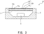
- a light-emitting device 21 of the second embodiment includes a ceramic container 3; a light-emitting element 5 disposed in the interior of the container 3; and a plate-like optical wavelength conversion member 23 disposed so as to cover an opening 7 of the container 3, as in the case of the first embodiment.
- the antireflection layer 25 is a translucent layer formed of, for example, magnesium fluoride for preventing light reflection.
- light emitted from the light-emitting element 5 transmits through the dielectric multilayer film 13, and the wavelength of the light is converted in the interior of the ceramic plate 11.
- the wavelength-converted light is emitted to the outside through the antireflection layer 25.
- the second embodiment achieves the same effects as in the first embodiment. Since the optical wavelength conversion member 23 includes the antireflection layer 25, light emitted from the ceramic plate 11 to the outside is less likely reflected at the light radiation surface 11b. Thus, light is more effectively emitted from the optical wavelength conversion member 23 to the outside.
- optical wavelength conversion member samples (Nos. 1 to 43) each including a ceramic sintered body (i.e., ceramic plate) were prepared under the conditions shown in Tables 1 and 2 below. Samples Nos. 2 to 17, 19 to 26, and 28 to 43 fall within the scope of the present invention (the aforementioned first aspect), and samples Nos. 1, 18, and 27 (i.e., samples of Comparative Examples) fall outside the scope of the present invention (the aforementioned first aspect).
- the weighed powder materials were added to a ball mill together with pure water, a specific amount of a binder (20 wt.% in terms of solid content, relative to the raw material powders), and a dispersant (1 wt.% in terms of solid content, relative to the raw material powders), and these materials were grind-mixed for 12 hours.
- the resultant slurry was formed into a sheet compact by means of doctor blading.
- the sheet compact was degreased and then fired in an air atmosphere at 1,450°C to 1,750°C for 3 to 20 hours.
- Ceramic sintered bodies for samples Nos. 1 to 43 were prepared.
- Each ceramic sintered body had a plate form (a rectangular parallelepiped shape) and dimensions of 20 mm ⁇ 20 mm ⁇ 0.5 mm (thickness).
- the surface roughness of a ceramic sintered body was adjusted by using abrasive grains with different sizes during mirror polishing of both surfaces (in a thickness direction) of the ceramic sintered body.
- the porosity of the above-prepared ceramic sintered body was measured by means of a microscope (manufactured by Keyence Corporation). Specifically, the mirror-polished surface of the ceramic sintered body was observed, and an image (x 500) was obtained at any position of the surface. The image was subjected to image processing, to thereby calculate the porosity.
- the average surface roughness Sa (i.e., arithmetic average roughness Sa) of the mirror-polished surface of each ceramic sintered body was measured by means of a non-contact three-dimensional measuring apparatus Infinite Focus G5 (manufactured by Alicona Imaging). The results are shown in Table 2 below.
- the average surface roughness Sa (i.e., arithmetic average roughness Sa) is a three-dimensional extension of two-dimensional arithmetic average roughness Ra and is a parameter standardized by ISO 25178.
- a dielectric multilayer film was formed on one surface (in a thickness direction) (i.e., a light incident surface) of the above-mirror-polished ceramic sintered body by means of sputtering.
- an optical wavelength conversion member i.e., sample
- a dielectric multilayer film (in which the number of layers and the thicknesses thereof were regulated) was formed to achieve optical properties such that when light is vertically incident on the light incident surface of each ceramic sintered body (i.e., ceramic plate), the dielectric multilayer film transmits 90% or more of light having a wavelength of 350 to 480 nm and reflects 90% or more of light having a wavelength of 500 nm or more.
- a multilayer film having such optical properties can be formed through stacking of 40 layers (overall thickness: 3 ⁇ m) by use of titanium oxide and silicon oxide.
- a dielectric multilayer film having the aforementioned properties can be formed by alternate stacking of titanium oxide layers and silicon oxide layers under control of the thicknesses of the layers.
- the dielectric multilayer film may be formed by means of vacuum deposition or ion plating in place of sputtering.
- the density of each ceramic sintered body was measured by the Archimedes method, and the measured density was converted into a relative density.
- Blue LD light (wavelength: 465 nm) was focused to a width of 0.5 mm by means of a lens, and the surface of each sample on which the dielectric multilayer film was formed was irradiated with the focused light.
- the light transmitting through the sample was focused by means of a lens, and the emission intensity was measured by means of a power sensor.
- the sample was irradiated with the light at a power density of 40 W/mm 2 .
- the emission intensity was evaluated by a value relative to that (taken as 100) of a YAG:Ce single-crystal body.
- Variation in color was evaluated through determination of a variation in chromaticity by means of a color illuminometer.
- Blue LD light (wavelength: 465 nm) was focused to a width of 0.3 mm by means of a lens, and the surface of each sample on which the dielectric multilayer film was formed was irradiated with the focused light.
- a color illuminometer was used to determine the chromaticity of the light transmitting through the surface of the sample opposite the surface irradiated with the focused light.
- the light irradiation was performed on a 18 mm square region (at intervals of 3 mm in the region) at the center of the irradiation surface of the sample, and a variation in chromaticity (in X-direction) (i.e., a variation in color: color unevenness) was evaluated.
- a variation in chromaticity in X-direction
- color unevenness i.e., a variation in color: color unevenness
- Each optical wavelength conversion member sample having the dielectric multilayer film was cut in a thickness direction, and the cut surface was subjected to mirror polishing. Subsequently, the mirror-polished surface was observed under a scanning electron microscope (i.e., SEM observation), and images ( ⁇ 5,000) were obtained any portions of the interface between the dielectric multilayer film and the ceramic plate. The images were joined together so that the interfacial length reached 100 ⁇ m or more. In the resultant image, the number of pores present at the interface was counted, and the opening sizes of the pores were measured.
- interface refers to the interface between the dielectric multilayer film and the ceramic plate.
- maximum pore opening size refers to the maximum of opening sizes of a plurality of pores at the interface (specifically at a line of 100 ⁇ m along the cross section).
- Example 1 each ceramic sintered body was prepared so that the YAG content of the ceramic sintered body was 21 vol.% and the Ce content was 0.7 mol% relative to Y in YAG.
- the surface roughness (average surface roughness Sa) of the ceramic sintered body was modified, and a dielectric multilayer film was formed on the surface having modified average surface roughness Sa, to thereby prepare a sample.
- the sample was evaluated for its properties. The results are shown in Table 2 below.
- sample No. 1 which was provided with no dielectric multilayer film, exhibited slightly low fluorescence intensity.
- Samples Nos. 2 to 8 which had an average surface roughness Sa of 0.5 ⁇ m or less and were provided with a dielectric multilayer film, exhibited high fluorescence intensity and reduced variation in color. That is, these samples exhibited good results in terms of fluorescence intensity and variation in color.
- sample No. 9 which had an average surface roughness Sa of more than 0.5 ⁇ m, exhibited low fluorescence intensity and increased variation in color.
- Example 1 All the samples of Example 1 exhibited a relative density of 99% or more; i.e., the samples were sufficiently densified.
- Example 2 as shown in Tables 1 and 2 below, samples (Nos. 10 to 18) were prepared and evaluated in the same manner as in Example 1.
- each ceramic sintered body was prepared so that the YAG content of the ceramic sintered body was 21 vol.% and the Ce content was 0.7 mol% relative to Y in YAG.
- the porosity of the ceramic sintered body was regulated under control of firing conditions.
- a dielectric multilayer film was formed on the surface having modified average surface roughness Sa, to thereby prepare a sample. The sample was evaluated for its properties.
- sample No. 17 which had a maximum pore opening size of more than 2 ⁇ m at the dielectric multilayer film/ceramic plate interface, exhibited high fluorescence intensity but increased variation in color.
- Samples Nos. 20 to 25 which had a YAG content of the ceramic sintered body of 5 to 50 vol.%, exhibited good results in terms of fluorescence intensity and variation in color. That is, these examples exhibited high fluorescence intensity and reduced variation in color.
- Sample No. 36 exhibited reduced variation in color but low fluorescence intensity.
Landscapes
- Chemical & Material Sciences (AREA)
- Engineering & Computer Science (AREA)
- Physics & Mathematics (AREA)
- Materials Engineering (AREA)
- Organic Chemistry (AREA)
- Ceramic Engineering (AREA)
- General Physics & Mathematics (AREA)
- Optics & Photonics (AREA)
- Structural Engineering (AREA)
- Inorganic Chemistry (AREA)
- Spectroscopy & Molecular Physics (AREA)
- Condensed Matter Physics & Semiconductors (AREA)
- Electromagnetism (AREA)
- Manufacturing & Machinery (AREA)
- General Engineering & Computer Science (AREA)
- Composite Materials (AREA)
- Luminescent Compositions (AREA)
- Compositions Of Oxide Ceramics (AREA)
- Optical Filters (AREA)
- Led Device Packages (AREA)
- Surface Treatment Of Optical Elements (AREA)
- Semiconductor Lasers (AREA)
Applications Claiming Priority (2)
| Application Number | Priority Date | Filing Date | Title |
|---|---|---|---|
| JP2017034682A JP2018141035A (ja) | 2017-02-27 | 2017-02-27 | 光波長変換部材及び発光装置 |
| PCT/JP2017/040613 WO2018154869A1 (ja) | 2017-02-27 | 2017-11-10 | 光波長変換部材及び発光装置 |
Publications (2)
| Publication Number | Publication Date |
|---|---|
| EP3588151A1 true EP3588151A1 (de) | 2020-01-01 |
| EP3588151A4 EP3588151A4 (de) | 2021-02-17 |
Family
ID=63254196
Family Applications (1)
| Application Number | Title | Priority Date | Filing Date |
|---|---|---|---|
| EP17898117.1A Withdrawn EP3588151A4 (de) | 2017-02-27 | 2017-11-10 | Lichtwellenlängenumwandlungselement und lichtemittierende vorrichtung |
Country Status (7)
| Country | Link |
|---|---|
| US (1) | US11214731B2 (de) |
| EP (1) | EP3588151A4 (de) |
| JP (1) | JP2018141035A (de) |
| KR (1) | KR102243598B1 (de) |
| CN (1) | CN110325884B (de) |
| TW (1) | TWI663141B (de) |
| WO (1) | WO2018154869A1 (de) |
Cited By (1)
| Publication number | Priority date | Publication date | Assignee | Title |
|---|---|---|---|---|
| CN111875370A (zh) * | 2020-07-07 | 2020-11-03 | 中国科学院上海光学精密机械研究所 | 一种用于蓝光led或ld激发的复合晶相荧光陶瓷及其制备方法 |
Families Citing this family (11)
| Publication number | Priority date | Publication date | Assignee | Title |
|---|---|---|---|---|
| EP3549923B1 (de) * | 2018-04-05 | 2025-09-03 | Nichia Corporation | Verfahren zur herstellung eines keramischen komplexes |
| JP7260740B2 (ja) * | 2018-12-07 | 2023-04-19 | 日亜化学工業株式会社 | セラミックス複合体、それを用いた発光装置及びセラミックス複合体の製造方法 |
| JP7148797B2 (ja) | 2018-12-20 | 2022-10-06 | 日亜化学工業株式会社 | 希土類アルミン酸塩蛍光体の製造方法、希土類アルミン酸塩蛍光体及び発光装置 |
| US11205886B2 (en) * | 2019-03-12 | 2021-12-21 | Nichia Corporation | Method of manufacturing optical member, optical member, and light emitting device |
| US11530798B2 (en) * | 2019-04-18 | 2022-12-20 | Nippon Electric Glass Co., Ltd. | Wavelength conversion member, method for manufacturing same, and light emission device |
| JP7157898B2 (ja) * | 2019-08-09 | 2022-10-21 | 株式会社タムラ製作所 | 波長変換部材 |
| JP7617364B2 (ja) | 2020-08-07 | 2025-01-20 | 日亜化学工業株式会社 | 希土類アルミン酸塩焼結体及びその製造方法 |
| JP7695509B2 (ja) | 2020-12-11 | 2025-06-19 | 日亜化学工業株式会社 | セラミックス複合体、発光装置及びセラミックス複合体の製造方法 |
| CN114806577B (zh) | 2021-01-22 | 2024-10-29 | 中强光电股份有限公司 | 波长转换材料及其制造方法、波长转换装置以及投影装置 |
| KR20230001983A (ko) * | 2021-06-29 | 2023-01-05 | 대주전자재료 주식회사 | 파장 변환 부재 및 이를 포함하는 발광장치 |
| JP7767257B2 (ja) * | 2021-12-28 | 2025-11-11 | クアーズテック合同会社 | セラミックス蛍光体プレート |
Family Cites Families (18)
| Publication number | Priority date | Publication date | Assignee | Title |
|---|---|---|---|---|
| JPS54143100A (en) | 1978-04-28 | 1979-11-07 | Mitsubishi Heavy Ind Ltd | Labeling machine |
| CA2116950A1 (en) | 1993-03-22 | 1994-09-23 | Pamela K. Whitman | Lamp with ir reflecting film and light-scattering coating |
| US7256057B2 (en) * | 2004-09-11 | 2007-08-14 | 3M Innovative Properties Company | Methods for producing phosphor based light sources |
| CN100566490C (zh) * | 2005-03-14 | 2009-12-02 | 皇家飞利浦电子股份有限公司 | 多晶陶瓷结构中的磷光体和包括该磷光体的发光元件 |
| JP5490407B2 (ja) | 2005-03-14 | 2014-05-14 | コーニンクレッカ フィリップス エヌ ヴェ | 多結晶セラミック構造の蛍光体、及び前記蛍光体を有する発光素子 |
| DE102006027133A1 (de) * | 2006-06-12 | 2007-12-13 | Merck Patent Gmbh | Verfahren zur Herstellung von Granat-Leuchtstoffen in einem Pulsationsreaktor |
| JP5650885B2 (ja) | 2008-12-27 | 2015-01-07 | 日亜化学工業株式会社 | 波長変換焼結体及びこれを用いた発光装置、並びに波長変換焼結体の製造方法 |
| EP2531571A1 (de) * | 2010-02-04 | 2012-12-12 | Nitto Denko Corporation | Lichtdurchlässiges keramiklaminat und herstellungsverfahren dafür |
| WO2012014360A1 (ja) | 2010-07-26 | 2012-02-02 | 株式会社小糸製作所 | 発光モジュール |
| JP5088977B2 (ja) | 2010-08-18 | 2012-12-05 | コバレントマテリアル株式会社 | セラミックス複合体 |
| JP5740017B2 (ja) | 2012-03-30 | 2015-06-24 | コバレントマテリアル株式会社 | セラミックス複合体 |
| JP2013227481A (ja) | 2012-03-30 | 2013-11-07 | Covalent Materials Corp | セラミックス複合体 |
| JP6056724B2 (ja) | 2013-09-30 | 2017-01-11 | ウシオ電機株式会社 | 蛍光光源装置 |
| JP6253392B2 (ja) * | 2013-12-18 | 2017-12-27 | スタンレー電気株式会社 | 発光装置及びそれを用いたプロジェクター用光源 |
| MY177277A (en) | 2014-03-03 | 2020-09-10 | Covalent Mat Corporation | Wavelength converting member |
| JP6233978B2 (ja) * | 2014-03-03 | 2017-11-22 | クアーズテック株式会社 | 波長変換焼成体 |
| JP6302762B2 (ja) | 2014-06-23 | 2018-03-28 | スタンレー電気株式会社 | 発光装置および照明装置 |
| JP2016060859A (ja) * | 2014-09-19 | 2016-04-25 | クアーズテック株式会社 | 蛍光体 |
-
2017
- 2017-02-27 JP JP2017034682A patent/JP2018141035A/ja active Pending
- 2017-11-10 KR KR1020197024924A patent/KR102243598B1/ko active Active
- 2017-11-10 US US16/488,847 patent/US11214731B2/en active Active
- 2017-11-10 EP EP17898117.1A patent/EP3588151A4/de not_active Withdrawn
- 2017-11-10 CN CN201780087449.8A patent/CN110325884B/zh active Active
- 2017-11-10 WO PCT/JP2017/040613 patent/WO2018154869A1/ja not_active Ceased
-
2018
- 2018-02-22 TW TW107105900A patent/TWI663141B/zh active
Cited By (1)
| Publication number | Priority date | Publication date | Assignee | Title |
|---|---|---|---|---|
| CN111875370A (zh) * | 2020-07-07 | 2020-11-03 | 中国科学院上海光学精密机械研究所 | 一种用于蓝光led或ld激发的复合晶相荧光陶瓷及其制备方法 |
Also Published As
| Publication number | Publication date |
|---|---|
| WO2018154869A1 (ja) | 2018-08-30 |
| US11214731B2 (en) | 2022-01-04 |
| TW201840509A (zh) | 2018-11-16 |
| EP3588151A4 (de) | 2021-02-17 |
| US20200392401A1 (en) | 2020-12-17 |
| TWI663141B (zh) | 2019-06-21 |
| CN110325884B (zh) | 2022-05-03 |
| CN110325884A (zh) | 2019-10-11 |
| KR102243598B1 (ko) | 2021-04-22 |
| KR20190105653A (ko) | 2019-09-17 |
| JP2018141035A (ja) | 2018-09-13 |
Similar Documents
| Publication | Publication Date | Title |
|---|---|---|
| US11214731B2 (en) | Light wavelength conversion member and light emitting device | |
| US11316078B2 (en) | Optical wavelength converter and composite optical device | |
| US9868270B2 (en) | Wavelength converting member | |
| JP6233978B2 (ja) | 波長変換焼成体 | |
| EP3438229A1 (de) | Fluoreszierender körper, lichtemittierende vorrichtung, beleuchtungsvorrichtung und bildanzeigevorrichtung | |
| EP3534192B1 (de) | Lichtwellenlängenumwandlungselement und lichtemittierende vorrichtung | |
| CN109642156B (zh) | 烧结荧光体、发光装置、照明装置和车辆用显示灯 | |
| EP3816682B1 (de) | Optisches wellenlängenumwandlungsbauteil, optische wellenlängenumwandlungsvorrichtung und lichtemittierende vorrichtung | |
| CN110342908A (zh) | 陶瓷复合体、投影仪用光源和陶瓷复合体的制造方法 | |
| EP3534190A1 (de) | Lichtwellenlängenumwandlungselement und lichtemittierende vorrichtung | |
| EP3822671B1 (de) | Optisches wellenlängenumwandlungselement und lichtemittierende vorrichtung | |
| JP2018072607A (ja) | 光波長変換部材及び発光装置 | |
| CN114695626A (zh) | 荧光体板 | |
| JP7628927B2 (ja) | 蛍光体プレート | |
| JP2025087512A (ja) | 波長変換部材、および発光装置 | |
| WO2024063115A1 (ja) | 波長変換部材および発光装置 | |
| JP2025036060A (ja) | 波長変換部材 | |
| CN121773359A (zh) | 波长转换部件 |
Legal Events
| Date | Code | Title | Description |
|---|---|---|---|
| STAA | Information on the status of an ep patent application or granted ep patent |
Free format text: STATUS: THE INTERNATIONAL PUBLICATION HAS BEEN MADE |
|
| PUAI | Public reference made under article 153(3) epc to a published international application that has entered the european phase |
Free format text: ORIGINAL CODE: 0009012 |
|
| STAA | Information on the status of an ep patent application or granted ep patent |
Free format text: STATUS: REQUEST FOR EXAMINATION WAS MADE |
|
| 17P | Request for examination filed |
Effective date: 20190827 |
|
| AK | Designated contracting states |
Kind code of ref document: A1 Designated state(s): AL AT BE BG CH CY CZ DE DK EE ES FI FR GB GR HR HU IE IS IT LI LT LU LV MC MK MT NL NO PL PT RO RS SE SI SK SM TR |
|
| AX | Request for extension of the european patent |
Extension state: BA ME |
|
| DAV | Request for validation of the european patent (deleted) | ||
| DAX | Request for extension of the european patent (deleted) | ||
| A4 | Supplementary search report drawn up and despatched |
Effective date: 20210115 |
|
| RIC1 | Information provided on ipc code assigned before grant |
Ipc: G02B 5/28 20060101ALI20210111BHEP Ipc: C09K 11/80 20060101ALI20210111BHEP Ipc: G02B 5/20 20060101AFI20210111BHEP Ipc: C09K 11/08 20060101ALI20210111BHEP Ipc: H01S 5/02 20060101ALI20210111BHEP Ipc: H01L 33/50 20100101ALI20210111BHEP Ipc: C04B 35/505 20060101ALI20210111BHEP Ipc: C09K 11/77 20060101ALI20210111BHEP Ipc: C09K 11/02 20060101ALI20210111BHEP |
|
| STAA | Information on the status of an ep patent application or granted ep patent |
Free format text: STATUS: THE APPLICATION HAS BEEN WITHDRAWN |
|
| 18W | Application withdrawn |
Effective date: 20210611 |