EP3589104A1 - Protection d'interférence électromagnétique (emi) - Google Patents
Protection d'interférence électromagnétique (emi) Download PDFInfo
- Publication number
- EP3589104A1 EP3589104A1 EP19175731.9A EP19175731A EP3589104A1 EP 3589104 A1 EP3589104 A1 EP 3589104A1 EP 19175731 A EP19175731 A EP 19175731A EP 3589104 A1 EP3589104 A1 EP 3589104A1
- Authority
- EP
- European Patent Office
- Prior art keywords
- shield plate
- pcb
- coupled
- emi shield
- enclosed area
- Prior art date
- Legal status (The legal status is an assumption and is not a legal conclusion. Google has not performed a legal analysis and makes no representation as to the accuracy of the status listed.)
- Granted
Links
Images


Classifications
-
- H—ELECTRICITY
- H05—ELECTRIC TECHNIQUES NOT OTHERWISE PROVIDED FOR
- H05K—PRINTED CIRCUITS; CASINGS OR CONSTRUCTIONAL DETAILS OF ELECTRIC APPARATUS; MANUFACTURE OF ASSEMBLAGES OF ELECTRICAL COMPONENTS
- H05K1/00—Printed circuits
- H05K1/02—Details
- H05K1/0213—Electrical arrangements not otherwise provided for
- H05K1/0216—Reduction of cross-talk, noise or electromagnetic interference
- H05K1/0218—Reduction of cross-talk, noise or electromagnetic interference by printed shielding conductors, ground planes or power plane
-
- H—ELECTRICITY
- H05—ELECTRIC TECHNIQUES NOT OTHERWISE PROVIDED FOR
- H05K—PRINTED CIRCUITS; CASINGS OR CONSTRUCTIONAL DETAILS OF ELECTRIC APPARATUS; MANUFACTURE OF ASSEMBLAGES OF ELECTRICAL COMPONENTS
- H05K9/00—Screening of apparatus or components against electric or magnetic fields
- H05K9/0007—Casings
- H05K9/002—Casings with localised screening
- H05K9/0022—Casings with localised screening of components mounted on printed circuit boards [PCB]
- H05K9/0037—Housings with compartments containing a PCB, e.g. partitioning walls
-
- G—PHYSICS
- G06—COMPUTING OR CALCULATING; COUNTING
- G06F—ELECTRIC DIGITAL DATA PROCESSING
- G06F1/00—Details not covered by groups G06F3/00 - G06F13/00 and G06F21/00
- G06F1/16—Constructional details or arrangements
- G06F1/1613—Constructional details or arrangements for portable computers
- G06F1/1633—Constructional details or arrangements of portable computers not specific to the type of enclosures covered by groups G06F1/1615 - G06F1/1626
- G06F1/1635—Details related to the integration of battery packs and other power supplies such as fuel cells or integrated AC adapter
-
- G—PHYSICS
- G06—COMPUTING OR CALCULATING; COUNTING
- G06F—ELECTRIC DIGITAL DATA PROCESSING
- G06F1/00—Details not covered by groups G06F3/00 - G06F13/00 and G06F21/00
- G06F1/16—Constructional details or arrangements
- G06F1/1613—Constructional details or arrangements for portable computers
- G06F1/1633—Constructional details or arrangements of portable computers not specific to the type of enclosures covered by groups G06F1/1615 - G06F1/1626
- G06F1/1656—Details related to functional adaptations of the enclosure, e.g. to provide protection against EMI, shock, water, or to host detachable peripherals like a mouse or removable expansions units like PCMCIA cards, or to provide access to internal components for maintenance or to removable storage supports like CDs or DVDs, or to mechanically mount accessories
-
- G—PHYSICS
- G06—COMPUTING OR CALCULATING; COUNTING
- G06F—ELECTRIC DIGITAL DATA PROCESSING
- G06F1/00—Details not covered by groups G06F3/00 - G06F13/00 and G06F21/00
- G06F1/16—Constructional details or arrangements
- G06F1/18—Packaging or power distribution
- G06F1/181—Enclosures
- G06F1/182—Enclosures with special features, e.g. for use in industrial environments; grounding or shielding against radio frequency interference [RFI] or electromagnetical interference [EMI]
-
- H—ELECTRICITY
- H05—ELECTRIC TECHNIQUES NOT OTHERWISE PROVIDED FOR
- H05K—PRINTED CIRCUITS; CASINGS OR CONSTRUCTIONAL DETAILS OF ELECTRIC APPARATUS; MANUFACTURE OF ASSEMBLAGES OF ELECTRICAL COMPONENTS
- H05K9/00—Screening of apparatus or components against electric or magnetic fields
- H05K9/0007—Casings
- H05K9/002—Casings with localised screening
- H05K9/0022—Casings with localised screening of components mounted on printed circuit boards [PCB]
- H05K9/0024—Shield cases mounted on a PCB, e.g. cans or caps or conformal shields
- H05K9/0026—Shield cases mounted on a PCB, e.g. cans or caps or conformal shields integrally formed from metal sheet
-
- H—ELECTRICITY
- H05—ELECTRIC TECHNIQUES NOT OTHERWISE PROVIDED FOR
- H05K—PRINTED CIRCUITS; CASINGS OR CONSTRUCTIONAL DETAILS OF ELECTRIC APPARATUS; MANUFACTURE OF ASSEMBLAGES OF ELECTRICAL COMPONENTS
- H05K9/00—Screening of apparatus or components against electric or magnetic fields
- H05K9/0007—Casings
- H05K9/0043—Casings being flexible containers, e.g. pouch, pocket, bag
-
- H—ELECTRICITY
- H05—ELECTRIC TECHNIQUES NOT OTHERWISE PROVIDED FOR
- H05K—PRINTED CIRCUITS; CASINGS OR CONSTRUCTIONAL DETAILS OF ELECTRIC APPARATUS; MANUFACTURE OF ASSEMBLAGES OF ELECTRICAL COMPONENTS
- H05K9/00—Screening of apparatus or components against electric or magnetic fields
- H05K9/0073—Shielding materials
- H05K9/0081—Electromagnetic shielding materials, e.g. EMI, RFI shielding
- H05K9/0084—Electromagnetic shielding materials, e.g. EMI, RFI shielding comprising a single continuous metallic layer on an electrically insulating supporting structure, e.g. metal foil, film, plating coating, electro-deposition, vapour-deposition
-
- H—ELECTRICITY
- H10—SEMICONDUCTOR DEVICES; ELECTRIC SOLID-STATE DEVICES NOT OTHERWISE PROVIDED FOR
- H10W—GENERIC PACKAGES, INTERCONNECTIONS, CONNECTORS OR OTHER CONSTRUCTIONAL DETAILS OF DEVICES COVERED BY CLASS H10
- H10W42/00—Arrangements for protection of devices
- H10W42/20—Arrangements for protection of devices protecting against electromagnetic or particle radiation, e.g. light, X-rays, gamma-rays or electrons
-
- H—ELECTRICITY
- H05—ELECTRIC TECHNIQUES NOT OTHERWISE PROVIDED FOR
- H05K—PRINTED CIRCUITS; CASINGS OR CONSTRUCTIONAL DETAILS OF ELECTRIC APPARATUS; MANUFACTURE OF ASSEMBLAGES OF ELECTRICAL COMPONENTS
- H05K2201/00—Indexing scheme relating to printed circuits covered by H05K1/00
- H05K2201/04—Assemblies of printed circuits
- H05K2201/047—Box-like arrangements of PCBs
-
- H—ELECTRICITY
- H05—ELECTRIC TECHNIQUES NOT OTHERWISE PROVIDED FOR
- H05K—PRINTED CIRCUITS; CASINGS OR CONSTRUCTIONAL DETAILS OF ELECTRIC APPARATUS; MANUFACTURE OF ASSEMBLAGES OF ELECTRICAL COMPONENTS
- H05K2201/00—Indexing scheme relating to printed circuits covered by H05K1/00
- H05K2201/05—Flexible printed circuits [FPCs]
- H05K2201/055—Folded back on itself
-
- H—ELECTRICITY
- H05—ELECTRIC TECHNIQUES NOT OTHERWISE PROVIDED FOR
- H05K—PRINTED CIRCUITS; CASINGS OR CONSTRUCTIONAL DETAILS OF ELECTRIC APPARATUS; MANUFACTURE OF ASSEMBLAGES OF ELECTRICAL COMPONENTS
- H05K2201/00—Indexing scheme relating to printed circuits covered by H05K1/00
- H05K2201/10—Details of components or other objects attached to or integrated in a printed circuit board
- H05K2201/10227—Other objects, e.g. metallic pieces
- H05K2201/10371—Shields or metal cases
-
- H—ELECTRICITY
- H05—ELECTRIC TECHNIQUES NOT OTHERWISE PROVIDED FOR
- H05K—PRINTED CIRCUITS; CASINGS OR CONSTRUCTIONAL DETAILS OF ELECTRIC APPARATUS; MANUFACTURE OF ASSEMBLAGES OF ELECTRICAL COMPONENTS
- H05K3/00—Apparatus or processes for manufacturing printed circuits
- H05K3/46—Manufacturing multilayer circuits
- H05K3/4688—Composite multilayer circuits, i.e. comprising insulating layers having different properties
- H05K3/4691—Rigid-flexible multilayer circuits comprising rigid and flexible layers, e.g. having in the bending regions only flexible layers
Definitions
- Embodiments of the present disclosure generally relate to the field of electromagnetic interference (EMI) shielding.
- EMI electromagnetic interference
- On-board EMI shield parts may have one or more drawbacks.
- on-board EMI shield parts may require PCB real estate for shielding tracks/mounting holes.
- EMI shield parts may suffer from warpage during manufacturing, or additional parts such as EMI gaskets may be needed. Some parts may require additional manufacturing steps such as solder reflow.
- the additional on-board shielding tracks and assembly requirements may occupy a relatively large board area, which may require a larger board width.
- the larger board width may come at the cost of battery size, thereby decreasing the overall battery life of a mobile device using the on-board shielding tracks.
- Mechanical mounted shielding can via mounting holes may have an even larger impact on the board width and routing.
- phrase “A or B” means (A), (B), or (A and B).
- phrase “A, B, or C” means (A), (B), (C), (A and B), (A and C), (B and C), or (A, B and C).
- Coupled may mean one or more of the following. “Coupled” may mean that two or more elements are in direct physical or electrical contact. However, “coupled” may also mean that two or more elements indirectly contact each other, but yet still cooperate or interact with each other, and may mean that one or more other elements are coupled or connected between the elements that are said to be coupled with each other.
- directly coupled may mean that two or elements are in direct contact.
- the phrase "a first feature formed, deposited, or otherwise disposed on a second feature,” may mean that the first feature is formed, deposited, or disposed over the feature layer, and at least a part of the first feature may be in direct contact (e.g., direct physical or electrical contact) or indirect contact (e.g., having one or more other features between the first feature and the second feature) with at least a part of the second feature.
- direct contact e.g., direct physical or electrical contact
- indirect contact e.g., having one or more other features between the first feature and the second feature
- module may refer to, be part of, or include an application specific integrated circuit (ASIC), an electronic circuit, a processor (shared, dedicated, or group) or memory (shared, dedicated, or group) that execute one or more software or firmware programs, a combinational logic circuit, or other suitable components that provide the described functionality.
- ASIC application specific integrated circuit
- processor shared, dedicated, or group
- memory shared, dedicated, or group
- Embodiments herein may relate to a robust EMI shielded wraparound technology which may use edge fingers/plating, guide holes, fiducial pads, or pre-bent flex edges.
- the EMI shielded wraparound technology may be combined with three-dimensional (3D) printed circuit board (PCB) technology to create an x/y/z space optimized solution that may enable smaller form factors for a shielded PCB.
- 3D three-dimensional
- PCB printed circuit board
- embodiments herein may relate to a built-in wraparound EMI shielding solution that may incorporate the folding of a 3D PCB technology to create a final assembled PCB assembly (PCBA) that is shielded in itself without the need for an additional on-board EMI shield.
- PCBA PCB assembly
- the outer most layer on the flex portion of a rigid-flex stackup may be used as an EMI layer that fold and wraps the inner components, for example, in a boxed-shape manner.
- the wrapped PCBA may then be robustly assembled together using a combination of edge finger pads, guide holes, fiducial parts, side EMI spacers, or pre-bent flex edge(s).
- the components within the PCBA may be stacked on top of one another in the PCBA to achieve the thinnest possible configuration for the PCBA with a given set of components.
- Figure 1 illustrates a simplified top-down view of an example device 100, in accordance with various embodiments.
- the device 100 may include a flexible portion 110 that are coupled with one or more rigid portions such as rigid portions 105 and 115.
- the flexible portion 110 may be a flexible EMI shield portion, and the rigid portions 105 and 115 may be PCBs.
- the rigid portions 105 and 115 may be coupled with the flexible portion 110 via, for example, an adhesive, direct lamination, direct layer build-up, or some other manner. More specifically, the rigid portions 105 and 115 may be coupled with a surface of the flexible portion 110 via one of the techniques discussed above.
- the flexible portion 110 may be formed of a plurality of layers of material that may be coupled with one another via an adhesive material (glue, epoxy, etc), deposited directly onto one another, or otherwise layered upon one another.
- the layers may include, for example, signal layers, ground layers, power layers, etc.
- the flexible portion 110 may further include one or more layers of a flexible copper clad laminate (FCCL) which may be, for example, copper and a polyimide.
- FCCL flexible copper clad laminate
- an outer surface of the flexible portion 110 may include an EMI shield portion (not shown in Figure 1 as it would be on the opposite side of the device 100 than shown in Figure 1 ) that may include a flexible EMI-blocking material such as aluminum or copper.
- the flexible portion 110 may have a thickness (which may also be referred to as z-height) of approximately 0.28 millimeters (mm). In other embodiments the flexible portion 110 may have a thickness of between approximately 0.07 mm and approximately 0.42 mm. Generally, the thickness of the flexible portion 110 may be based on a number of factors such as design considerations of the platform in which the device 100 may be used or other factors, so the flexible portion 110 may be thicker or thinner.
- the rigid portions 105 or 115 may include a plurality of layers of material that may be coupled with one another via an adhesive material, deposited directly onto one another, or otherwise layered upon one another.
- the layers may include, for example, signal layers, ground layers, power layers, etc.
- the rigid portions may be PCBs with a core, or coreless PCBs.
- the PCBs may include one or more components 103 dispositioned thereon.
- the PCBs may include components 103 such as a memory, a processor, a storage, a graphics chip, or some other type of component.
- the rigid portions 105 or 110 may have a thickness of approximately .41 mm, while in other embodiments the rigid portions 105 or 110 may have a thickness between approximately 0.4 mm and approximately 1 mm. In some embodiments rigid portion 105 may have the same thickness as rigid portion 110, while in other embodiments the rigid portions 105 and 110 may have different thicknesses. Similarly to the flexible portion 110, the thickness of the rigid portions 105 or 110 may be based on a number of factors such as design considerations of the platform in which the device 100 may be used, the number/types of components on the PCB, or some other factor.
- the device 100 may generally be separated into five different portions. Namely, the device 100 may include a first portion 120, a second portion 125, a third portion 130, a fourth portion 135, and a fifth portion 140.
- the various portions 120/125/130/135/140 may be collectively referred to herein as "portions 120-140.”
- the portions 120-140 may be designated in Figure 1 by the lateral dashed lines.
- the flexible portion 110 may be creased or otherwise have some physical demarcation between portions 120-140. In other embodiments, the flexible portion 110 may have no physical demarcation between portions 120-140.
- the first portion 120 may refer to a portion of the flexible portion 110 along which the rigid portion 105 overlaps as shown in Figure 1 .
- the second portion 125 may refer to a portion of the flexible portion 110 between rigid portion 105 and rigid portion 115.
- the third portion 130 may refer to a portion of the flexible portion 110 along which the rigid portion 115 overlaps as shown in Figure 1 .
- the fourth portion 135 and the fifth portion 140 may refer to portions of the flexible portion 110 along which rigid portions 105 and 115 are not present.
- the term “width” may refer to a distance along the axis demarcated “W” in Figure 1 .
- the term “length” may refer to a distance along the axis demarcated “L” in Figure 1 .
- the thickness or z-height of the device 100 may refer to a distance along an axis perpendicular to both the W and L axes.
- the first portion and the third portion of the flexible portion may have approximately the same width as shown in Figure 5 .
- the width of the third portion 130 may be approximately equal to the combined width of the first portion 120 and the fifth portion 140, as will be described in further detail with respect to Figures 2 and 3 .
- the second portion 125 and the fourth portion 135 may have approximately the same width.
- the rigid portions 105 and 115 may have the same width as one another. In other embodiments, rigid portion 105 may be wider or narrower than rigid portion 115. In some embodiments, rigid portion 105 may be narrower than the first portion 120 of flexible portion 110, or the combined width of the first portion 120 and the fifth portion 140. In some embodiments, rigid portion 115 may be narrower than the third portion 130.
- the device 100 may include one or more EMI spacers such as EMI spacer 165 at one or both ends of the device 100.
- the EMI spacer 165 may be formed of a EMI shielding material such as aluminum, copper, or some other material as described above.
- the EMI spacer may have a height that is approximately equivalent to the second portion 125 of the flexible portion 110, and a width that is approximately equal to the third portion 130.
- the EMI spacer 165 may be coupled with a different portion of the flexible portion 110 such as the second portion 125, the fourth portion 135, or some other portion.
- the EMI spacer 165 may be relatively thin and have a length on the order of a millimeter to a few millimeters, however in some embodiments the EMI spacer 165 may be longer or shorter. In some embodiments the EMI spacer 165 may not be directly coupled with the flexible portion 110, but rather may be coupled with rigid portion 105 or 115. In some embodiments the EMI spacer 165 may be coupled with a plurality of the portions 120-140, rigid portion 105, or rigid portion 115. Although the EMI spacer 165 is depicted as being set back from the end of the flexible portion 110, in other embodiments the EMI spacer 165 may at least partially extend from the flexible portion 110 on one or both sides of the device 100.
- the device 100 may include one or more fiducials 170. As shown in Figure 1 , the fiducials 170 may be located at various points on the flexible portion 110, or in some embodiments the fiducials may be located on the rigid portions 105 or 115. The device 100 may have more or less fiducials 170 than shown in Figure 1 . As used herein, a fiducial may be a marker element that may be made out of a material such as copper, gold, a dielectric material, or some other type of material and positioned on the flexible portion 170 or the rigid portions 105/115. The fiducial may be circular as shown in Figure 1 , or may have some other shape or cross-section such as rectangular, triangular, a star pattern, etc.
- the fiducial may be used by a human or computer system during the manufacturing process to identify a general orientation and position of the board so that the manufacturing process (e.g., the placement of components on a rigid portion 105/115, the placement of the rigid portions 105/115 on the flexible portion 110, placement of one or more conductive traces or pads on the device 100, etc.) may be performed consistently from device to device.
- the manufacturing process e.g., the placement of components on a rigid portion 105/115, the placement of the rigid portions 105/115 on the flexible portion 110, placement of one or more conductive traces or pads on the device 100, etc.
- the device 100 may include one or more alignment holes 150.
- the alignment holes 150 may be features in the fifth portion 150 that may allow for better alignment when the device 100 is reshaped, as will be described below.
- the alignment holes 150 may be laser etched, physically drilled or otherwise cut out, chemically etched, etc.
- the alignment holes 150 may be generally circular as shown in Figure 1 , while in other embodiments the alignment holes 150 may have a different shape such as square, rectangular, star-shaped, etc.
- the device 100 may include one or more connection elements 160.
- the connection elements 160 may include a plurality of elements. However, in other embodiments, the connection elements 160 may include more or fewer elements or may be a single element.
- the connection elements may be pads such as gold pads, solder pads, an anisotropic conductive film (ACF), or some other type of pad with a relatively low melting point such that the material can be reflowed subsequent to reshaping (as described in further detail below).
- the connection elements may include clips, screws, bolts, rivets, some type of adhesive material that may not require reflow, or some other type of connection element.
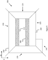
- FIG. 2 illustrates a simplified end-on view of the example device 100 of Figure 1 during reshaping, in accordance with various embodiments.
- the "width" of the device 100 is demarcated by the axis marked “W”
- the “height” or z-height of the device 100 is demarcated by the axis marked "Z.”
- the flexible portion 110 may be reshaped to generally from a box-like or rectangular-like shape as shown in Figure 2 .
- the device 100 may be reshaped along the lines indicated by the dashed lines in Figure 1 such that the first portion 120 is opposite the third portion 130, and the second portion 125 is opposite the fourth portion 135.
- the device 100 may be reshaped by a variety of processes.
- the flexible portion 110 may be reheated and then folded.
- the flexible portion 110 may not require heat but instead may be folded without a heating process.
- the flexible portion 110 may be otherwise softened such as through application of a chemical reactant such that the flexible portion 110 may be more easily folded. Some embodiments may use some other process, or a combination of various processes.
- the device may be reshaped such that the surface of the flexible portion 110 with which the rigid portion 105 and the rigid portion 115 are coupled is an inner surface 190 of the device.
- the surface of the flexible portion 110 opposite the inner surface 190 may be considered to be an outer surface 180 of the reshaped device 100.
- the device 100 may include one or more edge plate portions 107.
- the edge plate portions 107 may be formed of a conductive material such as copper, gold, or some other conductive material.
- the edge plate portions 107 may be positioned at an edge of a rigid portion such as rigid portion 105.
- the edge plate portions 107 may be coupled with, or include, one or more traces such as traces 109 or 111.
- Trace 109 may be on a surface of the rigid portion 105.
- Trace 111 may be internal to the rigid portion 105.
- the traces 109 or 111 may be communicatively coupled with components 103 of the rigid portion 105.
- the edge plate portions 107 may be manufactured by creating a row of plated through hole (PTH) vias coupled with internal power, ground, or signal layers of the rigid portion 105.
- the rigid portion may then be cut (e.g., via mechanical, optical, or chemical means) to expose the PTH vias at the edge of the rigid portion 105.
- PTH plated through hole
- the edge plate portions 107 may be pre-bent with a flex such as an approximately 90 degree flex as depicted in Figure 2 such that the edge plate portion 107 couples both with the rigid portion 105 both adjacent to the fourth portion 135 and the first portion 120.
- connection elements 160 may come into contact with the edge plate portion 107.
- various of the connection elements 160 or the edge plate portions 107 may be coupled with a variety of the components 103, or coupled with the EMI spacer 165.
- the connection elements 160, the edge plate portions 107, or the traces 109/111 may act to provide power or ground to the components 103, for example via an on-board power source that is coupled with one of rigid portions 115 or 105 or the flexible portion 110, or an external power source that is coupled with the device 100 via a port as described in further detail below.
- connection elements 160, edge plate portions 107, or the traces 109/111 may carry data signals between components 103 or between a component 103 and another device communicatively coupled with the device 100 via a port as described below.
- one or more of the edge plate portions 107 may not be present and the connection element 160 may couple directly with the rigid portion 105.
- FIG 3 illustrates a simplified end-on view of the example device 100 of Figure 1 subsequent to reshaping, in accordance with various embodiments.
- the reshaping process may be a reshaping process as discussed above.
- the fifth portion 140 may be coupled with the rigid portion 105 (for example, via the connection elements 160 or some other technique) and the fifth portion 140 may be adjacent to the first portion 120.
- the portions 120-140 may define an enclosed area 137 with the rigid portions 105/115 positioned therein.
- the rigid portions 105/115 may be EMI shielded by the flexible portion 110 and, in some embodiments, the EMI spacer 165.
- Figure 4 illustrates a simplified top-down view of the device 100 of Figure 1 subsequent to reshaping, in accordance with various embodiments.
- the third portion 180 may have a cutout portion 155 through which the rigid portion 115 may be accessible.
- the rigid portion 115 may be couplable, via the cutout portion 155, with a thermal solution such as a cooling element (not shown).
- the cooling element may be, for example, a heat sink, a fan, a vapor chamber, or some other type of cooling element.
- Figure 5 illustrates an alternative example device 200, which may be similar to device 100.
- the device 200 may have a flexible portion 210, rigid portions 205/215, a first portion 220, a second portion 225, and a third portion 230, which may be respectively similar to flexible portion 110, rigid portions 105/115, first portion 120, second portion 125, and third portion 130.
- Device 200 may have additional elements such as components, a cutout portion, edge plate portions, an EMI spacer, etc. as depicted with respect to device 100, however those elements may not be depicted in Figure 5 for the sake of clarity and elimination of redundancy.
- device 200 may include a fourth portion 235 that may be larger than the fourth portion 135 of device 100.
- the fifth portion 240 may not be coupled with rigid portion 205, but instead may instead be coupled with the outer surface 280 of first portion 220.
- the fifth portion 240 may be coupled with the first portion 220 via an adhesive, a solder material, or some other type of connection element such as connection element 160 described above.
- the cutout portion 155 may be located in a different portion 120-140 of the device 100, or there may be more cutout portions or no cutout portion.
- the edge plate portions 107 may be coupled with a different part of rigid portion 105, they may be additionally coupled with rigid portion 115, they may not exist, etc. There may be more or less edge plate portions 107, traces 109/111, components 103, rigid portions 105/115, etc.
- a rigid portion may additionally or alternatively be coupled with the inner surface of the second portion 125/225 or the fourth portion 135/235.
- the portions 120-140 may generally have a same length as one another.
- the flexible portion such as flexible portion 110/210 may not be rectangular, but rather one or more of the portions 120-140 (or equivalent portions of flexible portion 210) may have a greater length than another portion.
- one or more of the rigid portions 105/115/205/215 may have a greater length than the other rigid portion.
- the length of the portions of flexible portions 110/210 may be approximately equal to the length of rigid portions 105/115/205/215. In other embodiments, the length of the portions of flexible portions 110/210 may be greater than or less than the length of rigid portions 105/115/205/215.
- one or more of the rigid portions 105/115/205/215 is longer than the flexible portion 110/210, there may be one or more additional elements, components, or connectors coupled with the rigid portion 105/115/205/215 at a point that extends beyond the flexible portion 110/210.
- one or more of the portions of flexible portion 110/210 extend beyond another portion of flexible portion 110/210, or extend beyond rigid portions 105/115/205/215, there may be one or more additional elements, components, or connectors coupled with the extended portion of flexible portion 110/210.
- one of the additional connectors may include a port (not shown for clarity) that is operable to communicate with another device that is external to device 100/200.
- the connector may be operable to transmit/receive power, ground, or data signals to or from another device.
- the port may be a universal serial bus (USB) port, a display port, an M.2 socket for a modem, a m.2 socket for a solid state drive (SSD), or some other type of port, socket, or connector.
- USB universal serial bus
- the flexible portion 110 may have more or less portions.
- the flexible portion 110 may only have four portions which, when reshaped, may generally have a triangular cross-section when viewed end-on such as in Figure 2 .
- there may be additional portions such that the flexible portion 110, when reshaped, may generally have a pentagonal, hexagonal, circular, etc. cross-section.
- Figure 6 illustrates an example process for generating the example device 100 or 200 of Figures 1 or 5 , in accordance with various embodiments.
- the process may include identifying, at 305, a single EMI shield plate that includes a first surface with a PCB coupled thereto.
- the single EMI shield plate may be, for example, the flexible portion 110 or 210 described above.
- the first surface may be, for example, surface 190 (or the equivalent surface of device 200).
- the PCB may be, for example, rigid portions 105, 115, 205, or 215.
- the process may also include reshaping, at 310, the EMI shield plate to form a reshaped single EMI shield plate that defines an enclosed area, wherein the PCB is within the enclosed area.
- the reshaped single EMI shield plate may be, for example, device 100 as shown in Figures 3 or 4 , or device 200 as shown in Figure 5 .
- the enclosed area may be, for example, enclosed area 137 of device 100 (or the equivalent area of device 200).
- Embodiments herein may provide a variety of benefits. Specifically, by using a reshaped flexible portion, the device 100 or 200 may have a decreased x-y footprint in any device (such as a mobile device, a computer system, etc.) that uses device 100 or 200. For example, use of device 100 or 200 may result in an almost 40% reduction in x-y footprint. Additionally, use of device 100 or 200 may eliminate the need for an additional external EMI shielding can, which may result in significant cost savings. Finally, the reduction in x-y footprint may allow for a larger battery to be used alongside device 100 or 200, resulting in an overall increased battery life for any device hat uses device 100 or 200.
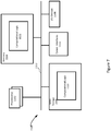
- Figure 7 illustrates an example computing device 1500 suitable for use with devices 100 or 200, in accordance with various embodiments.
- the computing device 1500 may include device 100 or 200 therein.
- computing device 1500 may include one or more processors or processor cores 1502 and system memory 1504.
- processors or processor cores 1502 and system memory 1504.
- the processor 1502 may include any type of processors, such as a central processing unit (CPU), a microprocessor, and the like.
- the processor 1502 may be implemented as an integrated circuit having multi-cores, e.g., a multi-core microprocessor.
- the computing device 1500 may include mass storage devices 1506 (such as diskette, hard drive, volatile memory (e.g., dynamic random-access memory (DRAM), compact disc read-only memory (CD-ROM), digital versatile disk (DVD), and so forth).
- DRAM dynamic random-access memory
- CD-ROM compact disc read-only memory
- DVD digital versatile disk
- system memory 1504 and/or mass storage devices 1506 may be temporal and/or persistent storage of any type, including, but not limited to, volatile and non-volatile memory, optical, magnetic, and/or solid state mass storage, and so forth.
- Volatile memory may include, but is not limited to, static and/or dynamic random-access memory.
- Non-volatile memory may include, but is not limited to, electrically erasable programmable read-only memory, phase change memory, resistive memory, and so forth.
- the computing device 1500 may further include input/output (I/O) devices 1508 (such as a display (e.g., a touchscreen display), keyboard, cursor control, remote control, gaming controller, image capture device, and so forth) and communication interfaces 1510 (such as network interface cards, modems, infrared receivers, radio receivers (e.g., Bluetooth), and so forth).
- I/O input/output
- the host device 103 may be elements of computing device 1500 such as processor(s) 1502, memory 1504, mass storage 1506, etc.
- the communication interfaces 1510 may include communication chips (not shown) that may be configured to operate the device 1500 in accordance with a Global System for Mobile Communication (GSM), General Packet Radio Service (GPRS), Universal Mobile Telecommunications System (UMTS), High Speed Packet Access (HSPA), Evolved HSPA (E-HSPA), or Long-Term Evolution (LTE) network.
- the communication chips may also be configured to operate in accordance with Enhanced Data for GSM Evolution (EDGE), GSM EDGE Radio Access Network (GERAN), Universal Terrestrial Radio Access Network (UTRAN), or Evolved UTRAN (E-UTRAN).
- EDGE Enhanced Data for GSM Evolution
- GERAN GSM EDGE Radio Access Network
- UTRAN Universal Terrestrial Radio Access Network
- E-UTRAN Evolved UTRAN
- the communication chips may be configured to operate in accordance with Code Division Multiple Access (CDMA), Time Division Multiple Access (TDMA), Digital Enhanced Cordless Telecommunications (DECT), Evolution-Data Optimized (EV-DO), derivatives thereof, as well as any other wireless protocols that are designated as 3G, 4G, 5G, and beyond.
- CDMA Code Division Multiple Access
- TDMA Time Division Multiple Access
- DECT Digital Enhanced Cordless Telecommunications
- EV-DO Evolution-Data Optimized
- derivatives thereof as well as any other wireless protocols that are designated as 3G, 4G, 5G, and beyond.
- the communication interfaces 1510 may operate in accordance with other wireless protocols in other embodiments.
- the above-described computing device 1500 elements may be coupled to each other via system bus 1512, which may represent one or more buses. In the case of multiple buses, they may be bridged by one or more bus bridges (not shown). Each of these elements may perform its conventional functions known in the art.
- the various elements may be implemented by assembler instructions supported by processor(s) 1502 or high-level languages that may be compiled into such instructions.
- the permanent copy of the programming instructions may be placed into mass storage devices 1506 in the factory, or in the field, through, for example, a distribution medium (not shown), such as a compact disc (CD), or through communication interface 1510 (from a distribution server (not shown)). That is, one or more distribution media having an implementation of the agent program may be employed to distribute the agent and to program various computing devices.
- a distribution medium such as a compact disc (CD)
- CD compact disc
- communication interface 1510 from a distribution server (not shown)
- the number, capability, and/or capacity of the elements 1508, 1510, 1512 may vary, depending on whether computing device 1500 is used as a stationary computing device, such as a set-top box or desktop computer, or a mobile computing device, such as a tablet computing device, laptop computer, game console, or smartphone. Their constitutions are otherwise known, and accordingly will not be further described.
- processors 1502 may be packaged together with computational logic 1522 configured to practice aspects of optical signal transmission and receipt described herein to form a System in Package (SiP) or a System on Chip (SoC).
- SiP System in Package
- SoC System on Chip
- the computing device 1500 may comprise one or more components of a data center, a laptop, a netbook, a notebook, an ultrabook, a smartphone, a tablet, a personal digital assistant (PDA), an ultra mobile PC, a mobile phone, or a digital camera.
- the computing device 1500 may be any other electronic device that processes data.
- various of the elements described with respect to computing device 1500 may be the components 103 of device 100 or 200.
- the processor(s) 1502, the memory 1504, the computational logic 1522, or the communications interface 1510 may be one of the components 103.
- the components may be coupled with another component of computing device 1500 via connection of the above-described port to system bus 1512.
- Various embodiments may include any suitable combination of the above-described embodiments including alternative (or) embodiments of embodiments that are described in conjunctive form (and) above (e.g., the "and” may be “and/or”).
- some embodiments may include one or more articles of manufacture (e.g., non-transitory computer-readable media) having instructions, stored thereon, that when executed result in actions of any of the above-described embodiments.
- some embodiments may include apparatuses or systems having any suitable means for carrying out the various operations of the above-described embodiments.
Landscapes
- Engineering & Computer Science (AREA)
- Microelectronics & Electronic Packaging (AREA)
- Theoretical Computer Science (AREA)
- Physics & Mathematics (AREA)
- Computer Hardware Design (AREA)
- General Engineering & Computer Science (AREA)
- Human Computer Interaction (AREA)
- General Physics & Mathematics (AREA)
- Electromagnetism (AREA)
- Power Engineering (AREA)
- Shielding Devices Or Components To Electric Or Magnetic Fields (AREA)
- Health & Medical Sciences (AREA)
- Toxicology (AREA)
Applications Claiming Priority (1)
| Application Number | Priority Date | Filing Date | Title |
|---|---|---|---|
| US16/016,997 US10701796B2 (en) | 2018-06-25 | 2018-06-25 | Electromagnetic interference (EMI) shield |
Publications (2)
| Publication Number | Publication Date |
|---|---|
| EP3589104A1 true EP3589104A1 (fr) | 2020-01-01 |
| EP3589104B1 EP3589104B1 (fr) | 2023-05-17 |
Family
ID=65230144
Family Applications (1)
| Application Number | Title | Priority Date | Filing Date |
|---|---|---|---|
| EP19175731.9A Active EP3589104B1 (fr) | 2018-06-25 | 2019-05-21 | Protection d'interférence électromagnétique (emi) |
Country Status (3)
| Country | Link |
|---|---|
| US (1) | US10701796B2 (fr) |
| EP (1) | EP3589104B1 (fr) |
| CN (1) | CN110636751A (fr) |
Cited By (1)
| Publication number | Priority date | Publication date | Assignee | Title |
|---|---|---|---|---|
| EP4016245A1 (fr) * | 2020-12-18 | 2022-06-22 | Intel Corporation | Enceinte de protection contre les interférences électromagnétiques à conductivité thermique |
Families Citing this family (3)
| Publication number | Priority date | Publication date | Assignee | Title |
|---|---|---|---|---|
| KR20230112396A (ko) | 2022-01-20 | 2023-07-27 | 에스케이하이닉스 주식회사 | 바텀 플래인의 길이를 변경하여 전자기 간섭을 회피하기 위한 솔리드 스테이트 드라이브 |
| US12300653B2 (en) | 2022-03-22 | 2025-05-13 | Toyota Motor Engineering & Manufacturing North America, Inc. | Electronics assemblies with power electronic devices and three-dimensionally printed circuit boards having reduced joule heating |
| US11792913B2 (en) | 2022-10-13 | 2023-10-17 | Google Llc | Mitigation of physical impact-induced mechanical stress damage to printed circuit boards |
Citations (6)
| Publication number | Priority date | Publication date | Assignee | Title |
|---|---|---|---|---|
| US5031027A (en) * | 1990-07-13 | 1991-07-09 | Motorola, Inc. | Shielded electrical circuit |
| US20060067070A1 (en) * | 2004-09-28 | 2006-03-30 | Sharp Kabushiki Kaisha | Radio frequency module and manufacturing method thereof |
| EP2091308A2 (fr) * | 2008-02-13 | 2009-08-19 | Siemens Medical Instruments Pte. Ltd. | Commutation dotée d'un blindage intégré et aide auditive |
| DE102010041831A1 (de) * | 2010-09-30 | 2012-04-05 | Automotive Lighting Reutlingen Gmbh | Elektronische Steuereinrichtung für eine Beleuchtungseinrichtung eines Kraftfahrzeugs |
| JP2012146823A (ja) * | 2011-01-12 | 2012-08-02 | Nippon Koden Corp | シールド方法及電子機器 |
| US20160192544A1 (en) * | 2014-12-26 | 2016-06-30 | Intel Corporation | Integrated thermal emi structure for electronic devices |
Family Cites Families (8)
| Publication number | Priority date | Publication date | Assignee | Title |
|---|---|---|---|---|
| US5107989A (en) * | 1990-02-05 | 1992-04-28 | Conductive Containers, Inc. | Container for protecting electronic components from static charges |
| EP1233666A4 (fr) * | 2000-06-06 | 2005-04-13 | Mitsubishi Electric Corp | Structure de refroidissement d'un dispositif de communication |
| US7248484B2 (en) * | 2003-03-12 | 2007-07-24 | Hewlett-Packard Development Company, L.P. | Electro-magnetic suppressive structure |
| JP4794819B2 (ja) * | 2003-04-02 | 2011-10-19 | キヤノン株式会社 | 電子機器 |
| JP5830858B2 (ja) * | 2010-12-24 | 2015-12-09 | 株式会社豊田自動織機 | 電子機器 |
| US8987872B2 (en) * | 2013-03-11 | 2015-03-24 | Qualcomm Incorporated | Electromagnetic interference enclosure for radio frequency multi-chip integrated circuit packages |
| US10368442B2 (en) * | 2015-03-30 | 2019-07-30 | Taiwan Semiconductor Manufacturing Company, Ltd. | Integrated circuit structure and method of forming |
| US10080282B2 (en) * | 2016-02-16 | 2018-09-18 | Kabushiki Kaisha Toshiba | Flexible printed circuit and electronic apparatus |
-
2018
- 2018-06-25 US US16/016,997 patent/US10701796B2/en active Active
-
2019
- 2019-05-21 EP EP19175731.9A patent/EP3589104B1/fr active Active
- 2019-05-24 CN CN201910438687.XA patent/CN110636751A/zh active Pending
Patent Citations (6)
| Publication number | Priority date | Publication date | Assignee | Title |
|---|---|---|---|---|
| US5031027A (en) * | 1990-07-13 | 1991-07-09 | Motorola, Inc. | Shielded electrical circuit |
| US20060067070A1 (en) * | 2004-09-28 | 2006-03-30 | Sharp Kabushiki Kaisha | Radio frequency module and manufacturing method thereof |
| EP2091308A2 (fr) * | 2008-02-13 | 2009-08-19 | Siemens Medical Instruments Pte. Ltd. | Commutation dotée d'un blindage intégré et aide auditive |
| DE102010041831A1 (de) * | 2010-09-30 | 2012-04-05 | Automotive Lighting Reutlingen Gmbh | Elektronische Steuereinrichtung für eine Beleuchtungseinrichtung eines Kraftfahrzeugs |
| JP2012146823A (ja) * | 2011-01-12 | 2012-08-02 | Nippon Koden Corp | シールド方法及電子機器 |
| US20160192544A1 (en) * | 2014-12-26 | 2016-06-30 | Intel Corporation | Integrated thermal emi structure for electronic devices |
Cited By (2)
| Publication number | Priority date | Publication date | Assignee | Title |
|---|---|---|---|---|
| EP4016245A1 (fr) * | 2020-12-18 | 2022-06-22 | Intel Corporation | Enceinte de protection contre les interférences électromagnétiques à conductivité thermique |
| US12167530B2 (en) | 2020-12-18 | 2024-12-10 | Intel Corporation | Electromagnetic interference shielding enclosure with thermal conductivity |
Also Published As
| Publication number | Publication date |
|---|---|
| EP3589104B1 (fr) | 2023-05-17 |
| US20190045621A1 (en) | 2019-02-07 |
| CN110636751A (zh) | 2019-12-31 |
| US10701796B2 (en) | 2020-06-30 |
Similar Documents
| Publication | Publication Date | Title |
|---|---|---|
| EP3589104A1 (fr) | Protection d'interférence électromagnétique (emi) | |
| US9568695B2 (en) | Package structure of optical connector | |
| US8102669B2 (en) | Chip package structure with shielding cover | |
| US11758662B2 (en) | Three dimensional foldable substrate with vertical side interface | |
| US10034393B2 (en) | Implementing high-speed signaling via dedicated printed circuit-board media | |
| US10729050B2 (en) | Fine pitch component placement on printed circuit boards | |
| KR101989516B1 (ko) | 반도체 패키지 | |
| WO2006110868A2 (fr) | Inductance | |
| EP3125069B1 (fr) | Structure et procédé de réduction d'interférence électromagnétique | |
| US20190303333A1 (en) | System with an interposer for high-speed memory modules | |
| EP4033866A1 (fr) | Régions métalliques pour protéger une source de champ magnétique | |
| CN103490229B (zh) | 电连接器组件 | |
| US8633398B2 (en) | Circuit board contact pads | |
| US8215966B2 (en) | Interposer connector assembly | |
| CN220691335U (zh) | 一种主板结构及该主板结构配套的机箱 | |
| US20250081348A1 (en) | Bridge printed circuit board embedded within another printed circuit board | |
| US11641710B1 (en) | Circuit board ground via patterns for minimizing crosstalk between signal vias | |
| JP6379428B2 (ja) | コネクタ、光電子接続部、及び、電子デバイスを製造する方法 | |
| CN206004117U (zh) | M.2 NVMe储存装置转接板 | |
| CN221010368U (zh) | 电路板组件及电子设备 | |
| CN216057643U (zh) | PCIe板卡 | |
| US7377806B1 (en) | Circuit board having at least one auxiliary scribed line | |
| KR20260045533A (ko) | 인식 마크를 포함하는 인쇄 회로 기판 및 이것을 포함하는 전자 장치 | |
| KR20260059518A (ko) | 다른 인쇄 회로 보드 내에 내장된 브리지 인쇄 회로 보드 | |
| JP2025049039A (ja) | 小型高速電気コネクタ及びその電子システム |
Legal Events
| Date | Code | Title | Description |
|---|---|---|---|
| PUAI | Public reference made under article 153(3) epc to a published international application that has entered the european phase |
Free format text: ORIGINAL CODE: 0009012 |
|
| STAA | Information on the status of an ep patent application or granted ep patent |
Free format text: STATUS: THE APPLICATION HAS BEEN PUBLISHED |
|
| AK | Designated contracting states |
Kind code of ref document: A1 Designated state(s): AL AT BE BG CH CY CZ DE DK EE ES FI FR GB GR HR HU IE IS IT LI LT LU LV MC MK MT NL NO PL PT RO RS SE SI SK SM TR |
|
| AX | Request for extension of the european patent |
Extension state: BA ME |
|
| STAA | Information on the status of an ep patent application or granted ep patent |
Free format text: STATUS: REQUEST FOR EXAMINATION WAS MADE |
|
| 17P | Request for examination filed |
Effective date: 20200630 |
|
| RBV | Designated contracting states (corrected) |
Designated state(s): AL AT BE BG CH CY CZ DE DK EE ES FI FR GB GR HR HU IE IS IT LI LT LU LV MC MK MT NL NO PL PT RO RS SE SI SK SM TR |
|
| STAA | Information on the status of an ep patent application or granted ep patent |
Free format text: STATUS: EXAMINATION IS IN PROGRESS |
|
| 17Q | First examination report despatched |
Effective date: 20210916 |
|
| REG | Reference to a national code |
Ref country code: DE Ref legal event code: R079 Ref document number: 602019029006 Country of ref document: DE Free format text: PREVIOUS MAIN CLASS: H05K0009000000 Ipc: G06F0001160000 |
|
| RIC1 | Information provided on ipc code assigned before grant |
Ipc: H01L 23/552 20060101ALI20220928BHEP Ipc: H05K 9/00 20060101ALI20220928BHEP Ipc: H05K 3/46 20060101ALI20220928BHEP Ipc: H05K 1/02 20060101ALI20220928BHEP Ipc: G06F 1/18 20060101ALI20220928BHEP Ipc: G06F 1/16 20060101AFI20220928BHEP |
|
| GRAP | Despatch of communication of intention to grant a patent |
Free format text: ORIGINAL CODE: EPIDOSNIGR1 |
|
| STAA | Information on the status of an ep patent application or granted ep patent |
Free format text: STATUS: GRANT OF PATENT IS INTENDED |
|
| INTG | Intention to grant announced |
Effective date: 20221130 |
|
| GRAS | Grant fee paid |
Free format text: ORIGINAL CODE: EPIDOSNIGR3 |
|
| GRAA | (expected) grant |
Free format text: ORIGINAL CODE: 0009210 |
|
| STAA | Information on the status of an ep patent application or granted ep patent |
Free format text: STATUS: THE PATENT HAS BEEN GRANTED |
|
| AK | Designated contracting states |
Kind code of ref document: B1 Designated state(s): AL AT BE BG CH CY CZ DE DK EE ES FI FR GB GR HR HU IE IS IT LI LT LU LV MC MK MT NL NO PL PT RO RS SE SI SK SM TR |
|
| REG | Reference to a national code |
Ref country code: GB Ref legal event code: FG4D |
|
| REG | Reference to a national code |
Ref country code: CH Ref legal event code: EP |
|
| REG | Reference to a national code |
Ref country code: DE Ref legal event code: R096 Ref document number: 602019029006 Country of ref document: DE |
|
| REG | Reference to a national code |
Ref country code: IE Ref legal event code: FG4D |
|
| REG | Reference to a national code |
Ref country code: AT Ref legal event code: REF Ref document number: 1568659 Country of ref document: AT Kind code of ref document: T Effective date: 20230615 |
|
| P01 | Opt-out of the competence of the unified patent court (upc) registered |
Effective date: 20230530 |
|
| PGFP | Annual fee paid to national office [announced via postgrant information from national office to epo] |
Ref country code: NL Payment date: 20230525 Year of fee payment: 5 Ref country code: FR Payment date: 20230523 Year of fee payment: 5 |
|
| REG | Reference to a national code |
Ref country code: NL Ref legal event code: FP |
|
| REG | Reference to a national code |
Ref country code: LT Ref legal event code: MG9D |
|
| REG | Reference to a national code |
Ref country code: AT Ref legal event code: MK05 Ref document number: 1568659 Country of ref document: AT Kind code of ref document: T Effective date: 20230517 |
|
| PG25 | Lapsed in a contracting state [announced via postgrant information from national office to epo] |
Ref country code: SE Free format text: LAPSE BECAUSE OF FAILURE TO SUBMIT A TRANSLATION OF THE DESCRIPTION OR TO PAY THE FEE WITHIN THE PRESCRIBED TIME-LIMIT Effective date: 20230517 Ref country code: PT Free format text: LAPSE BECAUSE OF FAILURE TO SUBMIT A TRANSLATION OF THE DESCRIPTION OR TO PAY THE FEE WITHIN THE PRESCRIBED TIME-LIMIT Effective date: 20230918 Ref country code: NO Free format text: LAPSE BECAUSE OF FAILURE TO SUBMIT A TRANSLATION OF THE DESCRIPTION OR TO PAY THE FEE WITHIN THE PRESCRIBED TIME-LIMIT Effective date: 20230817 Ref country code: ES Free format text: LAPSE BECAUSE OF FAILURE TO SUBMIT A TRANSLATION OF THE DESCRIPTION OR TO PAY THE FEE WITHIN THE PRESCRIBED TIME-LIMIT Effective date: 20230517 Ref country code: AT Free format text: LAPSE BECAUSE OF FAILURE TO SUBMIT A TRANSLATION OF THE DESCRIPTION OR TO PAY THE FEE WITHIN THE PRESCRIBED TIME-LIMIT Effective date: 20230517 |
|
| PGFP | Annual fee paid to national office [announced via postgrant information from national office to epo] |
Ref country code: GB Payment date: 20230525 Year of fee payment: 5 |
|
| PG25 | Lapsed in a contracting state [announced via postgrant information from national office to epo] |
Ref country code: RS Free format text: LAPSE BECAUSE OF FAILURE TO SUBMIT A TRANSLATION OF THE DESCRIPTION OR TO PAY THE FEE WITHIN THE PRESCRIBED TIME-LIMIT Effective date: 20230517 Ref country code: PL Free format text: LAPSE BECAUSE OF FAILURE TO SUBMIT A TRANSLATION OF THE DESCRIPTION OR TO PAY THE FEE WITHIN THE PRESCRIBED TIME-LIMIT Effective date: 20230517 Ref country code: LV Free format text: LAPSE BECAUSE OF FAILURE TO SUBMIT A TRANSLATION OF THE DESCRIPTION OR TO PAY THE FEE WITHIN THE PRESCRIBED TIME-LIMIT Effective date: 20230517 Ref country code: LT Free format text: LAPSE BECAUSE OF FAILURE TO SUBMIT A TRANSLATION OF THE DESCRIPTION OR TO PAY THE FEE WITHIN THE PRESCRIBED TIME-LIMIT Effective date: 20230517 Ref country code: IS Free format text: LAPSE BECAUSE OF FAILURE TO SUBMIT A TRANSLATION OF THE DESCRIPTION OR TO PAY THE FEE WITHIN THE PRESCRIBED TIME-LIMIT Effective date: 20230917 Ref country code: HR Free format text: LAPSE BECAUSE OF FAILURE TO SUBMIT A TRANSLATION OF THE DESCRIPTION OR TO PAY THE FEE WITHIN THE PRESCRIBED TIME-LIMIT Effective date: 20230517 Ref country code: GR Free format text: LAPSE BECAUSE OF FAILURE TO SUBMIT A TRANSLATION OF THE DESCRIPTION OR TO PAY THE FEE WITHIN THE PRESCRIBED TIME-LIMIT Effective date: 20230818 |
|
| PG25 | Lapsed in a contracting state [announced via postgrant information from national office to epo] |
Ref country code: FI Free format text: LAPSE BECAUSE OF FAILURE TO SUBMIT A TRANSLATION OF THE DESCRIPTION OR TO PAY THE FEE WITHIN THE PRESCRIBED TIME-LIMIT Effective date: 20230517 |
|
| REG | Reference to a national code |
Ref country code: CH Ref legal event code: PL |
|
| PG25 | Lapsed in a contracting state [announced via postgrant information from national office to epo] |
Ref country code: SK Free format text: LAPSE BECAUSE OF FAILURE TO SUBMIT A TRANSLATION OF THE DESCRIPTION OR TO PAY THE FEE WITHIN THE PRESCRIBED TIME-LIMIT Effective date: 20230517 |
|
| REG | Reference to a national code |
Ref country code: BE Ref legal event code: MM Effective date: 20230531 |
|
| PG25 | Lapsed in a contracting state [announced via postgrant information from national office to epo] |
Ref country code: SM Free format text: LAPSE BECAUSE OF FAILURE TO SUBMIT A TRANSLATION OF THE DESCRIPTION OR TO PAY THE FEE WITHIN THE PRESCRIBED TIME-LIMIT Effective date: 20230517 Ref country code: SK Free format text: LAPSE BECAUSE OF FAILURE TO SUBMIT A TRANSLATION OF THE DESCRIPTION OR TO PAY THE FEE WITHIN THE PRESCRIBED TIME-LIMIT Effective date: 20230517 Ref country code: RO Free format text: LAPSE BECAUSE OF FAILURE TO SUBMIT A TRANSLATION OF THE DESCRIPTION OR TO PAY THE FEE WITHIN THE PRESCRIBED TIME-LIMIT Effective date: 20230517 Ref country code: LU Free format text: LAPSE BECAUSE OF NON-PAYMENT OF DUE FEES Effective date: 20230521 Ref country code: LI Free format text: LAPSE BECAUSE OF NON-PAYMENT OF DUE FEES Effective date: 20230531 Ref country code: EE Free format text: LAPSE BECAUSE OF FAILURE TO SUBMIT A TRANSLATION OF THE DESCRIPTION OR TO PAY THE FEE WITHIN THE PRESCRIBED TIME-LIMIT Effective date: 20230517 Ref country code: DK Free format text: LAPSE BECAUSE OF FAILURE TO SUBMIT A TRANSLATION OF THE DESCRIPTION OR TO PAY THE FEE WITHIN THE PRESCRIBED TIME-LIMIT Effective date: 20230517 Ref country code: CZ Free format text: LAPSE BECAUSE OF FAILURE TO SUBMIT A TRANSLATION OF THE DESCRIPTION OR TO PAY THE FEE WITHIN THE PRESCRIBED TIME-LIMIT Effective date: 20230517 Ref country code: CH Free format text: LAPSE BECAUSE OF NON-PAYMENT OF DUE FEES Effective date: 20230531 |
|
| REG | Reference to a national code |
Ref country code: DE Ref legal event code: R097 Ref document number: 602019029006 Country of ref document: DE |
|
| PG25 | Lapsed in a contracting state [announced via postgrant information from national office to epo] |
Ref country code: MC Free format text: LAPSE BECAUSE OF FAILURE TO SUBMIT A TRANSLATION OF THE DESCRIPTION OR TO PAY THE FEE WITHIN THE PRESCRIBED TIME-LIMIT Effective date: 20230517 |
|
| REG | Reference to a national code |
Ref country code: IE Ref legal event code: MM4A |
|
| PG25 | Lapsed in a contracting state [announced via postgrant information from national office to epo] |
Ref country code: MC Free format text: LAPSE BECAUSE OF FAILURE TO SUBMIT A TRANSLATION OF THE DESCRIPTION OR TO PAY THE FEE WITHIN THE PRESCRIBED TIME-LIMIT Effective date: 20230517 |
|
| PLBE | No opposition filed within time limit |
Free format text: ORIGINAL CODE: 0009261 |
|
| STAA | Information on the status of an ep patent application or granted ep patent |
Free format text: STATUS: NO OPPOSITION FILED WITHIN TIME LIMIT |
|
| PG25 | Lapsed in a contracting state [announced via postgrant information from national office to epo] |
Ref country code: IE Free format text: LAPSE BECAUSE OF NON-PAYMENT OF DUE FEES Effective date: 20230521 |
|
| 26N | No opposition filed |
Effective date: 20240220 |
|
| PG25 | Lapsed in a contracting state [announced via postgrant information from national office to epo] |
Ref country code: IE Free format text: LAPSE BECAUSE OF NON-PAYMENT OF DUE FEES Effective date: 20230521 |
|
| PG25 | Lapsed in a contracting state [announced via postgrant information from national office to epo] |
Ref country code: SI Free format text: LAPSE BECAUSE OF FAILURE TO SUBMIT A TRANSLATION OF THE DESCRIPTION OR TO PAY THE FEE WITHIN THE PRESCRIBED TIME-LIMIT Effective date: 20230517 |
|
| PG25 | Lapsed in a contracting state [announced via postgrant information from national office to epo] |
Ref country code: SI Free format text: LAPSE BECAUSE OF FAILURE TO SUBMIT A TRANSLATION OF THE DESCRIPTION OR TO PAY THE FEE WITHIN THE PRESCRIBED TIME-LIMIT Effective date: 20230517 Ref country code: IT Free format text: LAPSE BECAUSE OF FAILURE TO SUBMIT A TRANSLATION OF THE DESCRIPTION OR TO PAY THE FEE WITHIN THE PRESCRIBED TIME-LIMIT Effective date: 20230517 Ref country code: BE Free format text: LAPSE BECAUSE OF NON-PAYMENT OF DUE FEES Effective date: 20230531 |
|
| PG25 | Lapsed in a contracting state [announced via postgrant information from national office to epo] |
Ref country code: BG Free format text: LAPSE BECAUSE OF FAILURE TO SUBMIT A TRANSLATION OF THE DESCRIPTION OR TO PAY THE FEE WITHIN THE PRESCRIBED TIME-LIMIT Effective date: 20230517 |
|
| PG25 | Lapsed in a contracting state [announced via postgrant information from national office to epo] |
Ref country code: BG Free format text: LAPSE BECAUSE OF FAILURE TO SUBMIT A TRANSLATION OF THE DESCRIPTION OR TO PAY THE FEE WITHIN THE PRESCRIBED TIME-LIMIT Effective date: 20230517 |
|
| REG | Reference to a national code |
Ref country code: NL Ref legal event code: MM Effective date: 20240601 |
|
| GBPC | Gb: european patent ceased through non-payment of renewal fee |
Effective date: 20240521 |
|
| PG25 | Lapsed in a contracting state [announced via postgrant information from national office to epo] |
Ref country code: NL Free format text: LAPSE BECAUSE OF NON-PAYMENT OF DUE FEES Effective date: 20240601 |
|
| PG25 | Lapsed in a contracting state [announced via postgrant information from national office to epo] |
Ref country code: FR Free format text: LAPSE BECAUSE OF NON-PAYMENT OF DUE FEES Effective date: 20240531 |
|
| PG25 | Lapsed in a contracting state [announced via postgrant information from national office to epo] |
Ref country code: GB Free format text: LAPSE BECAUSE OF NON-PAYMENT OF DUE FEES Effective date: 20240521 |
|
| PGFP | Annual fee paid to national office [announced via postgrant information from national office to epo] |
Ref country code: DE Payment date: 20250325 Year of fee payment: 7 |
|
| PG25 | Lapsed in a contracting state [announced via postgrant information from national office to epo] |
Ref country code: CY Free format text: LAPSE BECAUSE OF FAILURE TO SUBMIT A TRANSLATION OF THE DESCRIPTION OR TO PAY THE FEE WITHIN THE PRESCRIBED TIME-LIMIT; INVALID AB INITIO Effective date: 20190521 |
|
| PG25 | Lapsed in a contracting state [announced via postgrant information from national office to epo] |
Ref country code: HU Free format text: LAPSE BECAUSE OF FAILURE TO SUBMIT A TRANSLATION OF THE DESCRIPTION OR TO PAY THE FEE WITHIN THE PRESCRIBED TIME-LIMIT; INVALID AB INITIO Effective date: 20190521 |
|
| PG25 | Lapsed in a contracting state [announced via postgrant information from national office to epo] |
Ref country code: TR Free format text: LAPSE BECAUSE OF FAILURE TO SUBMIT A TRANSLATION OF THE DESCRIPTION OR TO PAY THE FEE WITHIN THE PRESCRIBED TIME-LIMIT Effective date: 20230517 |