EP3591945A1 - Connecteur usb à double couche de blindage - Google Patents
Connecteur usb à double couche de blindage Download PDFInfo
- Publication number
- EP3591945A1 EP3591945A1 EP17901868.4A EP17901868A EP3591945A1 EP 3591945 A1 EP3591945 A1 EP 3591945A1 EP 17901868 A EP17901868 A EP 17901868A EP 3591945 A1 EP3591945 A1 EP 3591945A1
- Authority
- EP
- European Patent Office
- Prior art keywords
- plug
- socket
- shield layer
- metal housing
- metal
- Prior art date
- Legal status (The legal status is an assumption and is not a legal conclusion. Google has not performed a legal analysis and makes no representation as to the accuracy of the status listed.)
- Pending
Links
Images



Classifications
-
- H—ELECTRICITY
- H01—ELECTRIC ELEMENTS
- H01R—ELECTRICALLY-CONDUCTIVE CONNECTIONS; STRUCTURAL ASSOCIATIONS OF A PLURALITY OF MUTUALLY-INSULATED ELECTRICAL CONNECTING ELEMENTS; COUPLING DEVICES; CURRENT COLLECTORS
- H01R13/00—Details of coupling devices of the kinds covered by groups H01R12/70 or H01R24/00 - H01R33/00
- H01R13/646—Details of coupling devices of the kinds covered by groups H01R12/70 or H01R24/00 - H01R33/00 specially adapted for high-frequency, e.g. structures providing an impedance match or phase match
- H01R13/6461—Means for preventing cross-talk
- H01R13/6464—Means for preventing cross-talk by adding capacitive elements
-
- H—ELECTRICITY
- H01—ELECTRIC ELEMENTS
- H01R—ELECTRICALLY-CONDUCTIVE CONNECTIONS; STRUCTURAL ASSOCIATIONS OF A PLURALITY OF MUTUALLY-INSULATED ELECTRICAL CONNECTING ELEMENTS; COUPLING DEVICES; CURRENT COLLECTORS
- H01R13/00—Details of coupling devices of the kinds covered by groups H01R12/70 or H01R24/00 - H01R33/00
- H01R13/648—Protective earth or shield arrangements on coupling devices, e.g. anti-static shielding
- H01R13/658—High frequency shielding arrangements, e.g. against EMI [Electro-Magnetic Interference] or EMP [Electro-Magnetic Pulse]
- H01R13/6591—Specific features or arrangements of connection of shield to conductive members
- H01R13/6592—Specific features or arrangements of connection of shield to conductive members the conductive member being a shielded cable
-
- H—ELECTRICITY
- H01—ELECTRIC ELEMENTS
- H01R—ELECTRICALLY-CONDUCTIVE CONNECTIONS; STRUCTURAL ASSOCIATIONS OF A PLURALITY OF MUTUALLY-INSULATED ELECTRICAL CONNECTING ELEMENTS; COUPLING DEVICES; CURRENT COLLECTORS
- H01R13/00—Details of coupling devices of the kinds covered by groups H01R12/70 or H01R24/00 - H01R33/00
- H01R13/648—Protective earth or shield arrangements on coupling devices, e.g. anti-static shielding
- H01R13/658—High frequency shielding arrangements, e.g. against EMI [Electro-Magnetic Interference] or EMP [Electro-Magnetic Pulse]
- H01R13/6598—Shield material
-
- H—ELECTRICITY
- H01—ELECTRIC ELEMENTS
- H01R—ELECTRICALLY-CONDUCTIVE CONNECTIONS; STRUCTURAL ASSOCIATIONS OF A PLURALITY OF MUTUALLY-INSULATED ELECTRICAL CONNECTING ELEMENTS; COUPLING DEVICES; CURRENT COLLECTORS
- H01R13/00—Details of coupling devices of the kinds covered by groups H01R12/70 or H01R24/00 - H01R33/00
- H01R13/66—Structural association with built-in electrical component
- H01R13/6608—Structural association with built-in electrical component with built-in single component
- H01R13/6625—Structural association with built-in electrical component with built-in single component with capacitive component
-
- H—ELECTRICITY
- H02—GENERATION; CONVERSION OR DISTRIBUTION OF ELECTRIC POWER
- H02J—ELECTRIC POWER NETWORKS; CIRCUIT ARRANGEMENTS OR SYSTEMS FOR SUPPLYING OR DISTRIBUTING ELECTRIC POWER; SYSTEMS FOR STORING ELECTRIC ENERGY
- H02J7/00—Circuit arrangements for charging or discharging batteries or for supplying loads from batteries
- H02J7/02—Circuit arrangements for charging or discharging batteries or for supplying loads from batteries for charging batteries from AC mains by converters
-
- H—ELECTRICITY
- H02—GENERATION; CONVERSION OR DISTRIBUTION OF ELECTRIC POWER
- H02J—ELECTRIC POWER NETWORKS; CIRCUIT ARRANGEMENTS OR SYSTEMS FOR SUPPLYING OR DISTRIBUTING ELECTRIC POWER; SYSTEMS FOR STORING ELECTRIC ENERGY
- H02J7/00—Circuit arrangements for charging or discharging batteries or for supplying loads from batteries
- H02J7/70—Circuit arrangements for charging or discharging batteries or for supplying loads from batteries characterised by the mechanical construction
-
- H—ELECTRICITY
- H01—ELECTRIC ELEMENTS
- H01B—CABLES; CONDUCTORS; INSULATORS; SELECTION OF MATERIALS FOR THEIR CONDUCTIVE, INSULATING OR DIELECTRIC PROPERTIES
- H01B11/00—Communication cables or conductors
- H01B11/02—Cables with twisted pairs or quads
- H01B11/06—Cables with twisted pairs or quads with means for reducing effects of electromagnetic or electrostatic disturbances, e.g. screens
- H01B11/10—Screens specially adapted for reducing interference from external sources
-
- H—ELECTRICITY
- H01—ELECTRIC ELEMENTS
- H01R—ELECTRICALLY-CONDUCTIVE CONNECTIONS; STRUCTURAL ASSOCIATIONS OF A PLURALITY OF MUTUALLY-INSULATED ELECTRICAL CONNECTING ELEMENTS; COUPLING DEVICES; CURRENT COLLECTORS
- H01R31/00—Coupling parts supported only by co-operation with counterpart
- H01R31/06—Intermediate parts for linking two coupling parts, e.g. adapter
-
- H—ELECTRICITY
- H02—GENERATION; CONVERSION OR DISTRIBUTION OF ELECTRIC POWER
- H02J—ELECTRIC POWER NETWORKS; CIRCUIT ARRANGEMENTS OR SYSTEMS FOR SUPPLYING OR DISTRIBUTING ELECTRIC POWER; SYSTEMS FOR STORING ELECTRIC ENERGY
- H02J2207/00—Details of circuit arrangements for charging or discharging batteries or supplying loads from batteries
- H02J2207/30—Charge provided using DC bus or data bus of a computer
Definitions
- Embodiments of the present invention relate to the communications field, and in particular, to reduction of electromagnetic interference to a terminal device.
- EMI Electromagnetic Interference
- electromagnetic interference harms performance of a device, a transmission channel, or a system, and threatens both stability and security of a terminal device.
- an embodiment of the present invention provides a universal serial bus (USB, Universal Serial Bus) connector, including: a first plug, where the first plug includes a first metal housing; a first socket, where the first socket includes the first metal housing, and the first socket is located in an enclosure of a terminal device; a second plug, where the second plug includes a second metal housing; and a second socket, where the second socket includes the second metal housing, and the second socket is located in an enclosure of an adapter, where the first plug is connected to the second plug by using a connection cable, the connection cable includes double layer shielded cables without electrical connection, the first metal housing of the first plug is connected to one end of a first-layer shielded cable, the other end of the first-layer shielded cable is suspended, the second metal housing of the second plug is connected to one end of a second-layer shielded cable, the other end of the second-layer shielded cable is suspended, and a capacitance between the first shield layer and the second shield layer is greater than a threshold.
- USB Universal Serial Bus
- the threshold may be 0.5 pF. In this embodiment, EMI can be better reduced.
- the first metal housing of the first socket is connected to an outer enclosure of the terminal device by using a capacitive component.
- the first metal housing of the first socket is connected to a ground cable by using a capacitive component.
- the capacitive component may be a capacitor or a transient voltage suppressor including a parasitic capacitor.
- a metal housing can be prevented from being floating, and a high-frequency interference signal is filtered out.
- the second metal housing of the second socket is connected to an outer enclosure of the adapter by using a capacitive component.
- the second metal housing of the second socket is connected to a ground terminal of the adapter by using a capacitive component.
- the capacitive component may be a capacitor or a transient voltage suppressor including a parasitic capacitor.
- a metal housing can be prevented from being floating, and a high-frequency interference signal is filtered out.
- An embodiment of the present invention provides a USB connector, including: a first plug, where the first plug includes a first metal housing; a first socket, where the first socket includes the first metal housing, and the first socket is located in an enclosure of a terminal device; a second plug, where the second plug includes a second metal housing; and a second socket, where the second socket includes the second metal housing, and the second socket is located in an enclosure of an adapter; where the first plug is connected to the second plug by using a connection cable, the connection cable includes a shielded cable, the first metal housing of the first plug is connected to one end of the shielded cable, the second metal housing of the second plug is connected to the other end of the shielded cable, the first metal housing of the first socket is grounded by using a capacitor, and the second metal housing of the second socket is grounded by using a capacitor.
- a metal housing can be prevented from being floating, and a high-frequency interference signal is filtered out.
- An embodiment of the present invention provides a terminal device, including a USB socket, where the USB socket includes a metal housing, at least one metal pin, and at least one cavity; and the metal housing of the USB socket is connected to an outer enclosure of the terminal device or a ground cable by using a capacitor.
- An embodiment of the present invention provides a charging system, including: a terminal device and an adapter, where the charging system uses the USB connector described above.
- EMI of the charging system can be reduced.
- the adapter may be replaced with a computer system.
- EMI of a system using the USB connector can be reduced in the embodiments of the present invention.
- USB universal serial bus
- USB Universal Serial Bus
- a "USB” in the present invention is a universal serial bus (English: Universal Serial Bus, USB for short), is a serial bus standard for connecting a computer system and an external device, and is also a technical specification of an input/output interface, widely applied to information communication products such as a personal computer and a mobile device, and extended to other related fields such as photographic equipment, a digital television (a set top box), and a game console.
- an electromagnetic interference condition may include an electromagnetic interference source, for example, a microprocessor, a microcontroller, a transmission container, an electrostatic discharge execution element, or an instantaneous power execution element.
- the electromagnetic interference condition may further include a coupling path. Noise coupled to a circuit is most easily transferred by a conductor through which the noise passes. For example, electromagnetic wave radiation exists in each circuit. In this case, circuit coupling is formed. When a current changes, electromagnetic waves are generated. These electromagnetic waves may be coupled to a surrounding conductor and interfere with other signals in the circuit.
- the electromagnetic interference condition may further include a receiver.
- All electronic circuits may be subject to electromagnetic interference. Although some electromagnetic interference is directly accepted in a form of radio-frequency radiation, most electromagnetic interference is accepted through transient conduction. In a digital circuit, critical signals such as a reset signal, an interruption signal, and a control signal are most vulnerable to electromagnetic interference. A control circuit, an analog low-level amplifier, and a power adjustment circuit are also vulnerable to noise.
- FIG. 1 is a first schematic diagram of a USB connector 100 according to a possible implementation of the present invention.
- the USB connector 100 includes a plug 001, a connection cable 002, a plug 003, a socket 004, and a socket 005.
- the USB connection cable 002 is connected to the plug 001 and the plug 003.
- the plug 001 and the plug 003 of the USB connector 100 may be combined at random.
- the USB plug 001 and the plug 003 may include any one of typeA, typeB, miniA, miniB, microA, microB, USBtypeA, USBtypeB, USBmicroB, and typeC.
- the plugs of the USB connector 100 correspondingly match the sockets of the USB connector 100.
- the plug 001 correspondingly matches the socket 004.
- the socket 004 and the socket 005 may be corresponding sockets, for example, may be any one of typeA, typeB, miniA, miniB, microA, microB, USBtypeA, USBtypeB, USBmicroB, and typeC.
- the plug 001 and the socket 004 of the USB connector 100 may be combined at random.
- a socket microAB may be combined with the plug microA or the plug microB.
- the USB connector 100 may use different versions, and a high version usually has downward compatibility.
- a USB 3.2 may be compatible with a USB 3.1, a USB 3.0, a USB 2.0, a USB 1.1, and a USB 1.0.
- FIG. 2 is a schematic diagram of a charging system according to a possible implementation of the present invention.
- one end of a USB connector is connected to a terminal device 006.
- the terminal device 006 in this embodiment of the present invention may include a mobile phone, a tablet computer, a PDA (Personal Digital Assistant, personal digital assistant), a POS (Point of Sales, point of sale), an in-vehicle computer, a TV, a wearable device, an AR device, a VR device, a portable music player, and the like.
- one end of the USB connector 100 may be further connected to a peripheral device.
- the peripheral device may include any one or more of a keyboard, a mouse, a modem, a printer, a scanner, a digital camera, a game handle, a hard disk, a network component, and the like.
- the other end of the USB connector 100 may be connected to an adapter 007, so as to supply power to the terminal device.
- the socket 004 and the socket 005 are respectively located on the adapter and the terminal device 100.
- the other end of the USB connector 100 may alternatively be a computer system.
- the computer system may include any one of a desktop computer, a notebook computer, a host computer, a controller board, and the like.
- both ends of the USB connector 100 may be connected to the terminal device.
- the mobile phone is connected to the portable music player by using the USB connector 100.
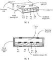
- FIG. 3 to FIG. 6 are a first schematic diagram to a fourth schematic diagram of a plug 001 of a USB connector 100 according to a possible implementation of the present invention.
- the first schematic diagram of the plug 001 of the USB connector 100 is provided.
- the plug 001 includes an enclosure 008, a metal housing 009, a pin 010, a pin 011, a pin 012, a pin 013, an insulation tongue 014, a cavity 015, and a fastening hole 016.
- the enclosure 008 may be an insulating plastic material.
- at least one of the pin 010, the pin 011, the pin 012, and the pin 013 is a power-supply pin, for example, the pin 010.
- at least one of the pin 010, the pin 011, the pin 012, and the pin 013 is a ground pin, for example, the pin 013.
- At least one of the pin 010, the pin 011, the pin 012, and the pin 013 is a data transmission pin, for example, the pin 011.
- the pin 010, the pin 011, the pin 012, and the pin 013 are attached to the insulation tongue 014.
- the cavity 015 is formed between an upper surface of the insulation tongue 014 and an inner side of an upper surface of the metal housing 009.
- a second schematic diagram of the plug 001 of the USB connector 100 is provided.
- the plug 001 includes a metal housing 009, a pin 010, a pin 011, a pin 012, a pin 013, an insulation tongue 014, a fastening hole 016, and a cavity 015.
- a third schematic diagram of the plug 001 of the USB connector 100 is provided.
- the plug 001 includes a metal housing 009, a pin 010, a pin 011, a pin 012, a pin 013, an insulation tongue 014, a connection cable 002, and a fastening terminal 017.
- the fourth schematic diagram of the plug 001 of the USB connector 100 is provided.
- the plug 001 includes a pin 010, a pin 011, a pin 012, a pin 013, an insulation tongue 014, and an enclosure 008.
- FIG. 7 is a schematic diagram of a socket 004 of a USB connector 100 according to a possible implementation of the present invention.
- the socket 004 includes a metal socket enclosure 018, an upper cavity 019, a lower cavity 020, an insulation tongue 021, a pin 022, a pin 023, a pin 024, a pin 025, and a socket enclosure 026.
- the pin 022, the pin 023, the pin 024, and the pin 025 are attached to an upper surface of the insulation tongue 021.
- the upper cavity 019 is formed between the upper surface of the insulation tongue 021 and an inside metal wall of an upper surface of the metal enclosure 018.
- the lower cavity 020 is formed between a lower surface of the insulation tongue 021 and an inside metal wall of a lower surface of the metal enclosure 018.
- the insulation tongue 014 of the plug 001 is inserted into the upper cavity 019 of the socket 004.
- the pin 010, the pin 011, the pin 012, and the pin 013 are respectively connected to the pin 022, the pin 023, the pin 024, and the pin 025 of the socket 004.
- the pin 010 is connected to the pin 022.
- one side of the metal housing 009 of the plug 001 (for example, an upper surface facing the insulation tongue 014) is inserted into the lower cavity 020.
- FIG. 8 is a second schematic diagram of a USB connector 100 according to a possible implementation of the present invention.
- a terminal-side ground 030, an adapter-side ground 029, and the metal housing 009 of the plug 001 are connected to the metal housing 018 of the socket 004, a metal housing 027 of the plug 003, a metal housing 028 of the socket 005, a shielded cable 031, and a ground cable 034.
- a signal cable 032, a power cable 033, and the ground cable 034 may be connected to pins (as shown in FIG. 7 ).
- the signal cable 032 may be connected to the pin 023 or the pin 024.
- the metal housing 018 of the socket 004 is connected to the metal housing 009 of the plug 001.
- FIG. 9 is a third schematic diagram of a USB connector 100 according to a possible implementation of the present invention.
- a connection between the shielded cable 031 and the metal plug housing 009 on a terminal side is disconnected.
- a connection between the shielded cable 031 and the metal plug housing 027 on an adapter side is disconnected.
- there may be no connection or the shielded cable 031 and the metal plug housing 027 may be connected by using an isolated electronic component.
- the metal housing 009 of the plug 001 on the terminal side and the metal housing 018 of the socket 004 are not grounded, for example, may be floating or suspended.
- the metal plug housing 027 on the adapter side and the metal socket housing 028 may not be grounded, for example, may be floating or suspended.
- this embodiment has an advantage that an overheating problem caused by a half-short circuit can be resolved.
- a spacing between the pin of the USB connector 100 and the metal housing 009 of the USB connector is increasingly small. Consequently, a half-short circuit is caused between a power supply and a GND after salt water or foreign matter enters and accumulates in a USB port. Such a state may cause overheating during charging, and may even cause burning.
- FIG. 10 is a fourth schematic diagram of a connector 100 according to a possible implementation of the present invention.
- a shielded cable 035 is added outside the shielded cable 031. Further, the shielded cable 035 may be added inside the shielded cable 031. In some embodiments, one end of the shielded cable 035 is connected to the metal plug housing 009, and the other end of the shielded cable layer 035 is disconnected from the metal plug housing 029. In some embodiments, when one end of the shielded cable 031 is connected to the metal plug enclosure 009, the other end of the shielded cable 031 is disconnected from the metal plug housing 027. In some embodiments, the shielded cable 031 and the shielded cable 035 are in a disconnected state.
- the shielded cable 031 and the shielded cable 035 may be made from metal shielding materials such as aluminum, zinc, copper, iron, steel, nickel, and an alloy thereof.
- the shielded cable 031 and the shielded cable 035 may be made from one or more of a conductive rubber, a metal woven mesh, a finger spring plate, and a plurality of conductive rubbers.
- a fifth schematic diagram of the connector 100 is further provided according to the fourth schematic diagram of the connector 100 provided in FIG. 10 .
- the shielded cable 031 forms a shield layer 1
- the shielded cable 035 forms another shield layer 2.
- a gap between the shielded cable 035 and the metal plug housing 027 may be considered as a capacitor C1.
- air or an insulating material may be a medium.
- the metal plug housing 027, the metal socket housing 028, and the shielded cable 031 are also connected.
- the capacitor C1 may also be considered as a capacitor between the shielded cable 031 and the shielded cable 035 or between the shielded cable 035 and the metal socket housing 028.
- the metal plug housing 009, the metal socket housing 018, and the shielded cable 035 are connected.
- the capacitor C1 is formed between the shielded cable 031 and the shielded cable 035.
- the capacitance may be adjusted by adjusting a distance between shielded cables.
- the capacitance of the capacitor C1 or a capacitor C2 directly affects high-frequency loop impedance.
- a formula for calculating loop impedance Z is: 1/j2 ⁇ fc, where f is frequency, and C is capacitance.
- electromagnetic interference is reduced by using a double-layer shielding technology, thereby effectively suppressing a noise current caused by electromagnetic wave radiation and conduction and a high-order harmonic wave.
- a high-frequency loop current may form a return current by using the capacitor C1, to form a similar state in which two ends are grounded, so as to implement magnetic field shielding, thereby suppressing EMI in a high-frequency magnetic field.
- this shield layer is incomplete, a gap between two shield layers is relatively small, so that the electromagnetic wave is shielded to some extent, thereby suppressing EMI.
- the shield layer is added to suppress EMI in the high-frequency magnetic field.
- FIG. 12 is a sixth schematic diagram of a connector 100 according to the present invention.
- the shielded cable 035 is located at an outer layer of the shielded cable 031. Further, there is no connection between the shielded cable 031 and the shielded cable 035.
- FIG. 13 is a seventh schematic diagram of a connector 100 according to a possible implementation of the present invention.
- the metal socket housing 018 is grounded by using several capacitive components (for example, the capacitor C2).
- the capacitive component may be a capacitor or a transient voltage suppressor including a parasitic capacitor.
- the metal plug housing 009 when the USB connector 100 is in a working state, to be specific, when the metal plug housing 009 is connected to the metal socket housing 018, it may be considered that the metal plug housing 009 and the metal socket housing 018 are grounded by using a capacitor (for example, the metal plug housing 009 and the metal socket housing 018 are connected to the terminal-side ground 030).
- the capacitor C2 may be a decoupling capacitor.
- high-frequency signal interference is removed.
- interference may be caused by electromagnetic radiation.
- the capacitor C2 is added to prevent the metal socket housing 018 and the metal plug housing 009 from being floating, and an EMI problem caused because a shielded cable layer has an aperture can be resolved.
- the EMI problem may be caused. Consequently, radiation of the terminal device 006 is too large to satisfy a security standard. However, the foregoing problem can be resolved in this embodiment.
- FIG. 14 is an eighth schematic diagram of a connector 100 according to a possible implementation of the present invention.
- the metal socket housing 028 is grounded by using several capacitive components (for example, may be a capacitor C3).
- the capacitive component may be a capacitor or a transient voltage suppressor including a parasitic capacitor.
- the capacitor C3 may be a decoupling capacitor.
- high-frequency signal interference is removed.
- interference may be caused by electromagnetic radiation.
- the metal plug housing 027 when the USB connector 100 is in a working state, to be specific, when the metal plug housing 027 is connected to the metal socket housing 028, it may be considered that the metal plug housing 027 and the metal socket housing 028 are grounded by using a capacitor (for example, the metal plug housing 027 and the metal socket housing 028 are connected to the adapter-side ground 029).
- a capacitor for example, the metal plug housing 027 and the metal socket housing 028 are connected to the adapter-side ground 029.
- the capacitor C3 is added to prevent the metal socket housing 027 and the metal plug housing 028 from being floating, and EMI that may be caused because a shielded cable layer has an aperture can be reduced.
- EMI that may be caused because a shielded cable layer has an aperture
- the terminal device 006 when the metal socket housing 018 is floating and a shield layer is incomplete, an EMI problem may be caused. Consequently, radiation of the terminal device 006 is too large to satisfy a security standard. However, EMI can be reduced in this embodiment.
- FIG. 15 is a ninth schematic diagram of a connector 100 according to a possible implementation of the present invention.
- the metal socket housing 018 is grounded by using several capacitive components (for example, a capacitor C4), and the metal socket housing 028 is grounded by using several capacitive components (for example, a capacitor C5).
- capacitive components are added to the metal socket housing 018 on the terminal side and the metal socket housing 028 on the adapter side for grounding, so that an entire USB connection system has no floating component, and there is no obvious aperture at a shield layer.
- system EMI is greatly reduced, and a filtering component optimizing solution that increases excessive costs is not required.
- FIG. 16 is a tenth schematic diagram of a connector 100 according to a possible implementation of the present invention.
- the metal socket housing 028 is connected by using several capacitive components (for example, a capacitor C6), and the metal socket housing 018 is connected by using several capacitive components (for example, a capacitor C7).
- both ends of the shielded cable 031 are respectively connected to the metal plug housing 009 and the metal plug housing 027.
- a solution of adding a shielded cable layer is not used.
- the capacitor C7 is added to prevent the metal socket housing 018 and the metal plug housing 009 from being floating
- the capacitor C6 is added to prevent the metal socket housing 027 and the metal plug housing 028 from being floating.
- a shield layer is complete, so that EMI of an entire system can be reduced.
- plug and socket in the present invention are not intended to limit the present invention, but for ease of description. In some embodiments, they may be interchanged or replaced.
- connection and “disconnected”, “disconnected state”, and “disconnected” in the present invention may be an electrical connection or electrical disconnection.
- a possible implementation of the present invention provides a low-EMI charging system.
- the system includes at least one terminal device 006, at least one USB connector 100, and at least one adapter 007.
- the charging system may alternatively be a data transmission system.
- the adapter 007 may be replaced with a computer system or the like.
- the charging system uses a connection manner of any circuit or several circuits described in FIG. 8 to FIG. 16 .
- a possible implementation of the present invention further provides a low-radiation terminal device 006.
- Capacitance grounding is mainly performed on a metal iron shell of a charging interface (for example, may be a typeC interface), so as to reduce electromagnetic interference during charging, thereby reducing device radiation.
- the present invention may be implemented by hardware, firmware, or a combination thereof.
- the foregoing functions may be stored in a computer-readable medium or transmitted as one or more instructions or code in the computer-readable medium.
- the computer-readable medium includes a computer storage medium and a communications medium, and the communications medium includes any medium that enables a computer program to be transmitted from one place to another.
- the storage medium may be any available medium accessible to a computer.
- the computer-readable medium may include a RAM, a ROM, an EEPROM, a CD-ROM or another optical disc storage or disk storage medium, or another magnetic storage device, or any other medium that can carry or store expected program code in a form of an instruction or a data structure and can be accessed by a computer.
- any connection may be appropriately defined as a computer-readable medium.
- the coaxial cable, optical fiber/cable, twisted pair, DSL or wireless technologies such as infrared ray, radio and microwave
- the coaxial cable, optical fiber/cable, twisted pair, DSL or wireless technologies such as infrared ray, radio and microwave are included in fixation of a medium to which they belong.
- a disk (Disk) and disc (disc) used in the present invention includes a compact disc (CD), a laser disc, an optical disc, a digital versatile disc (DVD), a floppy disk, and a Blu-ray disc, where the disk generally copies data by a magnetic means, and the disc copies data optically by a laser means.
Landscapes
- Engineering & Computer Science (AREA)
- Power Engineering (AREA)
- Details Of Connecting Devices For Male And Female Coupling (AREA)
- Insulated Conductors (AREA)
- Coupling Device And Connection With Printed Circuit (AREA)
Applications Claiming Priority (3)
| Application Number | Priority Date | Filing Date | Title |
|---|---|---|---|
| CN201710182214 | 2017-03-24 | ||
| CN201710931237 | 2017-10-09 | ||
| PCT/CN2017/113144 WO2018171241A1 (fr) | 2017-03-24 | 2017-11-27 | Connecteur usb à double couche de blindage |
Publications (2)
| Publication Number | Publication Date |
|---|---|
| EP3591945A1 true EP3591945A1 (fr) | 2020-01-08 |
| EP3591945A4 EP3591945A4 (fr) | 2020-02-26 |
Family
ID=63584775
Family Applications (1)
| Application Number | Title | Priority Date | Filing Date |
|---|---|---|---|
| EP17901868.4A Pending EP3591945A4 (fr) | 2017-03-24 | 2017-11-27 | Connecteur usb à double couche de blindage |
Country Status (4)
| Country | Link |
|---|---|
| US (1) | US11171454B2 (fr) |
| EP (1) | EP3591945A4 (fr) |
| JP (1) | JP2020523727A (fr) |
| WO (1) | WO2018171241A1 (fr) |
Cited By (3)
| Publication number | Priority date | Publication date | Assignee | Title |
|---|---|---|---|---|
| CN114267984A (zh) * | 2020-09-16 | 2022-04-01 | 安福烨翔精密电子有限公司 | 一种usb防水电连接器 |
| EP4318821A4 (fr) * | 2021-03-30 | 2024-10-09 | Vivo Mobile Communication Co., Ltd. | Ligne de données et dispositif électronique |
| EP4318820A4 (fr) * | 2021-03-30 | 2024-10-09 | Vivo Mobile Communication Co., Ltd. | Ligne de données et dispositif électronique |
Families Citing this family (4)
| Publication number | Priority date | Publication date | Assignee | Title |
|---|---|---|---|---|
| CN111740289A (zh) * | 2020-06-23 | 2020-10-02 | 维沃移动通信有限公司 | 一种数据线 |
| JP7670561B2 (ja) * | 2021-06-28 | 2025-04-30 | 日本航空電子工業株式会社 | コネクタ |
| CN115422102B (zh) * | 2021-10-08 | 2023-10-27 | 无锡宇宁智能科技有限公司 | USB、type-C接口电路及驱动板 |
| CN117374659B (zh) * | 2023-11-14 | 2024-07-30 | 东莞市煜锦实业有限公司 | 一种usb充电连接器 |
Family Cites Families (30)
| Publication number | Priority date | Publication date | Assignee | Title |
|---|---|---|---|---|
| US4236779A (en) | 1978-05-01 | 1980-12-02 | Bunker Ramo Corporation | EMI Shielded cable and connector assembly |
| US4477693A (en) | 1982-12-09 | 1984-10-16 | Cooper Industries, Inc. | Multiply shielded coaxial cable with very low transfer impedance |
| JPH01229292A (ja) | 1988-03-09 | 1989-09-12 | Mitsubishi Electric Corp | 表示装置 |
| JPH0632716Y2 (ja) * | 1988-08-04 | 1994-08-24 | 富士通株式会社 | 電子機器のシールド構造 |
| JPH0624143Y2 (ja) * | 1990-03-22 | 1994-06-22 | ソニーマグネスケール株式会社 | 同軸型コネクタの接続機構 |
| US5221216A (en) * | 1992-05-18 | 1993-06-22 | Amp Incorporated | Vertical mount connector |
| GB9415767D0 (en) * | 1994-08-04 | 1994-09-28 | Smiths Industries Plc | Filter assemblies |
| JPH08153545A (ja) | 1994-11-28 | 1996-06-11 | Oki Electric Ind Co Ltd | シールドケーブルの接続方法 |
| US6109971A (en) * | 1997-07-02 | 2000-08-29 | Adaptec, Inc. | High-speed serial data cable with improved electromagnetic performance |
| US5975958A (en) * | 1997-10-14 | 1999-11-02 | The Whitaker Corporation | Capactive coupling adapter for an electrical connector |
| CN2577472Y (zh) | 2002-07-19 | 2003-10-01 | 番禺得意精密电子工业有限公司 | 一种组合电连接器 |
| KR101164821B1 (ko) * | 2005-12-21 | 2012-07-12 | 삼성전자주식회사 | Usb케이블장치 및 디바이스 |
| US7794277B1 (en) * | 2009-06-19 | 2010-09-14 | F Time Technology Industrial Co., Ltd. | RF connector |
| US9728304B2 (en) * | 2009-07-16 | 2017-08-08 | Pct International, Inc. | Shielding tape with multiple foil layers |
| KR20120105445A (ko) | 2009-10-20 | 2012-09-25 | 사이프레스 세미컨덕터 코포레이션 | 터치 스크린 제어기에서의 결합 노이즈 영향을 감소시키기 위한 방법 및 장치 |
| US7927147B1 (en) * | 2009-12-15 | 2011-04-19 | Hewlett-Packard Development Company, L.P. | Connector assembly |
| CN201904509U (zh) * | 2010-10-21 | 2011-07-20 | 中广核工程有限公司 | 一种核电站控制电缆屏蔽层接地结构 |
| CN201887274U (zh) * | 2010-11-22 | 2011-06-29 | 富士康(昆山)电脑接插件有限公司 | 线缆连接器组件 |
| US8724662B2 (en) | 2012-06-25 | 2014-05-13 | Johnson & Johnson Vision Care, Inc. | Wireless communication protocol for low power receivers |
| FR2995100B1 (fr) * | 2012-09-05 | 2015-08-28 | Peugeot Citroen Automobiles Sa | Equipement electronique apte a generer une tension d'alimentation destinee a alimenter un appareil nomade |
| JP2014089944A (ja) * | 2012-10-01 | 2014-05-15 | Yazaki Corp | 同軸ケーブル |
| CN103516842B (zh) * | 2013-09-13 | 2016-05-11 | 广东欧珀移动通信有限公司 | 带天线的设备中的usb接口外壳切换电路 |
| CN203596646U (zh) * | 2013-12-10 | 2014-05-14 | 深圳怡化电脑股份有限公司 | 一种usb充电器 |
| CN104056796B (zh) | 2014-06-06 | 2016-09-14 | 深圳市泉峰精密机械有限公司 | Usb屏蔽线扫线装置 |
| TWI618305B (zh) | 2014-08-11 | 2018-03-11 | 英屬開曼群島商鴻騰精密科技股份有限公司 | 電連接器及其製造方法 |
| JP2016139295A (ja) | 2015-01-28 | 2016-08-04 | 京セラ株式会社 | 電子機器、電源アダプタ、および充電システム |
| CN105471041A (zh) | 2015-12-22 | 2016-04-06 | 张志平 | 一种电感式电源数据线及其制作方法 |
| CN105703181A (zh) | 2015-12-25 | 2016-06-22 | 北京长峰微电科技有限公司 | 一种usb数据emi屏蔽传输线 |
| JP6394721B2 (ja) * | 2017-03-03 | 2018-09-26 | 日立金属株式会社 | 同軸ケーブル |
| JP6380873B1 (ja) * | 2017-11-28 | 2018-08-29 | 日立金属株式会社 | 編組シールド付ケーブル |
-
2017
- 2017-11-27 WO PCT/CN2017/113144 patent/WO2018171241A1/fr not_active Ceased
- 2017-11-27 EP EP17901868.4A patent/EP3591945A4/fr active Pending
- 2017-11-27 US US16/496,814 patent/US11171454B2/en active Active
- 2017-11-27 JP JP2019552184A patent/JP2020523727A/ja active Pending
Cited By (4)
| Publication number | Priority date | Publication date | Assignee | Title |
|---|---|---|---|---|
| CN114267984A (zh) * | 2020-09-16 | 2022-04-01 | 安福烨翔精密电子有限公司 | 一种usb防水电连接器 |
| CN114267984B (zh) * | 2020-09-16 | 2023-06-09 | 安福烨翔精密电子有限公司 | 一种usb防水电连接器 |
| EP4318821A4 (fr) * | 2021-03-30 | 2024-10-09 | Vivo Mobile Communication Co., Ltd. | Ligne de données et dispositif électronique |
| EP4318820A4 (fr) * | 2021-03-30 | 2024-10-09 | Vivo Mobile Communication Co., Ltd. | Ligne de données et dispositif électronique |
Also Published As
| Publication number | Publication date |
|---|---|
| WO2018171241A1 (fr) | 2018-09-27 |
| US11171454B2 (en) | 2021-11-09 |
| EP3591945A4 (fr) | 2020-02-26 |
| JP2020523727A (ja) | 2020-08-06 |
| US20210104844A1 (en) | 2021-04-08 |
Similar Documents
| Publication | Publication Date | Title |
|---|---|---|
| US11171454B2 (en) | USB connector with double shield layers | |
| US8067701B2 (en) | I/O connectors with extendable faraday cage | |
| US6398588B1 (en) | Method and apparatus to reduce EMI leakage through an isolated connector housing using capacitive coupling | |
| CN103427162B (zh) | 电子装置 | |
| EP3673541B1 (fr) | Réceptacle d'émetteur-récepteur doté d'une cage emi et d'attaches de lunette qui offrent une efficacité de protection élevée | |
| CN110692169B (zh) | 便携式电子设备 | |
| JP2005510008A (ja) | コネクタからの電磁障害を低減するためのシールドの設置 | |
| US6413103B1 (en) | Method and apparatus for grounding microcoaxial cables inside a portable computing device | |
| WO2018068608A1 (fr) | Dispositif électronique | |
| TW201409866A (zh) | 公頭電連接器、母頭電連接器及電連接器組合 | |
| EP3125069B1 (fr) | Structure et procédé de réduction d'interférence électromagnétique | |
| CN100562241C (zh) | 防电磁干扰的电子装置 | |
| CN101242734A (zh) | 防电磁干扰遮蔽装置 | |
| US10181682B2 (en) | Ungrounded shield for an electrical connector | |
| CN108650560A (zh) | 一种兼顾电磁兼容与信号完整性的网口以及优化方法 | |
| CN109479074B (zh) | 双屏蔽层的usb连接器 | |
| CN111740289A (zh) | 一种数据线 | |
| CN108966558B (zh) | 一种服务器前置线缆的低辐射安装结构 | |
| US10249991B1 (en) | Low noise high-speed data connectors | |
| CN111435768A (zh) | 连接器 | |
| US7597572B2 (en) | Method and apparatus for improved universal serial bus connectivity having electrostatic discharge protection ground element | |
| US20060264102A1 (en) | Non-continuous counterpoise shield | |
| CN201741967U (zh) | 改良型网络连接装置 | |
| CN208111863U (zh) | 充电连接装置和充电系统 | |
| CN204905506U (zh) | 带有绝缘片的插座结构 |
Legal Events
| Date | Code | Title | Description |
|---|---|---|---|
| STAA | Information on the status of an ep patent application or granted ep patent |
Free format text: STATUS: THE INTERNATIONAL PUBLICATION HAS BEEN MADE |
|
| PUAI | Public reference made under article 153(3) epc to a published international application that has entered the european phase |
Free format text: ORIGINAL CODE: 0009012 |
|
| STAA | Information on the status of an ep patent application or granted ep patent |
Free format text: STATUS: REQUEST FOR EXAMINATION WAS MADE |
|
| 17P | Request for examination filed |
Effective date: 20191001 |
|
| AK | Designated contracting states |
Kind code of ref document: A1 Designated state(s): AL AT BE BG CH CY CZ DE DK EE ES FI FR GB GR HR HU IE IS IT LI LT LU LV MC MK MT NL NO PL PT RO RS SE SI SK SM TR |
|
| AX | Request for extension of the european patent |
Extension state: BA ME |
|
| A4 | Supplementary search report drawn up and despatched |
Effective date: 20200129 |
|
| RIC1 | Information provided on ipc code assigned before grant |
Ipc: H01B 11/18 20060101ALI20200123BHEP Ipc: H01B 11/10 20060101ALI20200123BHEP Ipc: H02J 7/00 20060101ALI20200123BHEP Ipc: H01R 13/648 20060101ALI20200123BHEP Ipc: H01B 11/06 20060101ALI20200123BHEP Ipc: H01R 31/06 20060101ALI20200123BHEP Ipc: H01R 13/6592 20110101ALI20200123BHEP Ipc: H01R 13/6464 20110101ALI20200123BHEP Ipc: H01R 13/6598 20110101ALI20200123BHEP Ipc: H01B 11/20 20060101ALI20200123BHEP Ipc: H04M 1/02 20060101AFI20200123BHEP Ipc: H01B 7/17 20060101ALI20200123BHEP |
|
| DAV | Request for validation of the european patent (deleted) | ||
| DAX | Request for extension of the european patent (deleted) | ||
| STAA | Information on the status of an ep patent application or granted ep patent |
Free format text: STATUS: EXAMINATION IS IN PROGRESS |
|
| 17Q | First examination report despatched |
Effective date: 20210429 |
|
| RIC1 | Information provided on ipc code assigned before grant |
Ipc: H01R 31/06 20060101ALN20220629BHEP Ipc: H02J 7/02 20160101ALI20220629BHEP Ipc: H01B 11/10 20060101ALI20220629BHEP Ipc: H01R 13/6598 20110101ALI20220629BHEP Ipc: H01R 13/6464 20110101ALI20220629BHEP Ipc: H01R 13/6592 20110101AFI20220629BHEP |