EP3595103A1 - Unité de source de lumière laser - Google Patents
Unité de source de lumière laser Download PDFInfo
- Publication number
- EP3595103A1 EP3595103A1 EP17899990.0A EP17899990A EP3595103A1 EP 3595103 A1 EP3595103 A1 EP 3595103A1 EP 17899990 A EP17899990 A EP 17899990A EP 3595103 A1 EP3595103 A1 EP 3595103A1
- Authority
- EP
- European Patent Office
- Prior art keywords
- laser oscillation
- housing
- electrode
- light source
- laser
- Prior art date
- Legal status (The legal status is an assumption and is not a legal conclusion. Google has not performed a legal analysis and makes no representation as to the accuracy of the status listed.)
- Withdrawn
Links
Images



Classifications
-
- H—ELECTRICITY
- H01—ELECTRIC ELEMENTS
- H01S—DEVICES USING THE PROCESS OF LIGHT AMPLIFICATION BY STIMULATED EMISSION OF RADIATION [LASER] TO AMPLIFY OR GENERATE LIGHT; DEVICES USING STIMULATED EMISSION OF ELECTROMAGNETIC RADIATION IN WAVE RANGES OTHER THAN OPTICAL
- H01S5/00—Semiconductor lasers
- H01S5/04—Processes or apparatus for excitation, e.g. pumping, e.g. by electron beams
- H01S5/042—Electrical excitation ; Circuits therefor
- H01S5/0425—Electrodes, e.g. characterised by the structure
- H01S5/04256—Electrodes, e.g. characterised by the structure characterised by the configuration
- H01S5/04257—Electrodes, e.g. characterised by the structure characterised by the configuration having positive and negative electrodes on the same side of the substrate
-
- H—ELECTRICITY
- H01—ELECTRIC ELEMENTS
- H01S—DEVICES USING THE PROCESS OF LIGHT AMPLIFICATION BY STIMULATED EMISSION OF RADIATION [LASER] TO AMPLIFY OR GENERATE LIGHT; DEVICES USING STIMULATED EMISSION OF ELECTROMAGNETIC RADIATION IN WAVE RANGES OTHER THAN OPTICAL
- H01S5/00—Semiconductor lasers
- H01S5/02—Structural details or components not essential to laser action
- H01S5/022—Mountings; Housings
- H01S5/02208—Mountings; Housings characterised by the shape of the housings
-
- H—ELECTRICITY
- H01—ELECTRIC ELEMENTS
- H01S—DEVICES USING THE PROCESS OF LIGHT AMPLIFICATION BY STIMULATED EMISSION OF RADIATION [LASER] TO AMPLIFY OR GENERATE LIGHT; DEVICES USING STIMULATED EMISSION OF ELECTROMAGNETIC RADIATION IN WAVE RANGES OTHER THAN OPTICAL
- H01S5/00—Semiconductor lasers
- H01S5/02—Structural details or components not essential to laser action
- H01S5/022—Mountings; Housings
- H01S5/02208—Mountings; Housings characterised by the shape of the housings
- H01S5/02212—Can-type, e.g. TO-CAN housings with emission along or parallel to symmetry axis
-
- H—ELECTRICITY
- H01—ELECTRIC ELEMENTS
- H01S—DEVICES USING THE PROCESS OF LIGHT AMPLIFICATION BY STIMULATED EMISSION OF RADIATION [LASER] TO AMPLIFY OR GENERATE LIGHT; DEVICES USING STIMULATED EMISSION OF ELECTROMAGNETIC RADIATION IN WAVE RANGES OTHER THAN OPTICAL
- H01S5/00—Semiconductor lasers
- H01S5/02—Structural details or components not essential to laser action
- H01S5/022—Mountings; Housings
- H01S5/0235—Method for mounting laser chips
- H01S5/02355—Fixing laser chips on mounts
-
- H—ELECTRICITY
- H01—ELECTRIC ELEMENTS
- H01S—DEVICES USING THE PROCESS OF LIGHT AMPLIFICATION BY STIMULATED EMISSION OF RADIATION [LASER] TO AMPLIFY OR GENERATE LIGHT; DEVICES USING STIMULATED EMISSION OF ELECTROMAGNETIC RADIATION IN WAVE RANGES OTHER THAN OPTICAL
- H01S5/00—Semiconductor lasers
- H01S5/02—Structural details or components not essential to laser action
- H01S5/022—Mountings; Housings
- H01S5/0235—Method for mounting laser chips
- H01S5/02355—Fixing laser chips on mounts
- H01S5/0237—Fixing laser chips on mounts by soldering
-
- H—ELECTRICITY
- H01—ELECTRIC ELEMENTS
- H01S—DEVICES USING THE PROCESS OF LIGHT AMPLIFICATION BY STIMULATED EMISSION OF RADIATION [LASER] TO AMPLIFY OR GENERATE LIGHT; DEVICES USING STIMULATED EMISSION OF ELECTROMAGNETIC RADIATION IN WAVE RANGES OTHER THAN OPTICAL
- H01S5/00—Semiconductor lasers
- H01S5/40—Arrangement of two or more semiconductor lasers, not provided for in groups H01S5/02 - H01S5/30
- H01S5/4018—Lasers electrically in series
-
- H—ELECTRICITY
- H01—ELECTRIC ELEMENTS
- H01S—DEVICES USING THE PROCESS OF LIGHT AMPLIFICATION BY STIMULATED EMISSION OF RADIATION [LASER] TO AMPLIFY OR GENERATE LIGHT; DEVICES USING STIMULATED EMISSION OF ELECTROMAGNETIC RADIATION IN WAVE RANGES OTHER THAN OPTICAL
- H01S5/00—Semiconductor lasers
- H01S5/40—Arrangement of two or more semiconductor lasers, not provided for in groups H01S5/02 - H01S5/30
- H01S5/4025—Array arrangements, e.g. constituted by discrete laser diodes or laser bar
-
- H—ELECTRICITY
- H01—ELECTRIC ELEMENTS
- H01S—DEVICES USING THE PROCESS OF LIGHT AMPLIFICATION BY STIMULATED EMISSION OF RADIATION [LASER] TO AMPLIFY OR GENERATE LIGHT; DEVICES USING STIMULATED EMISSION OF ELECTROMAGNETIC RADIATION IN WAVE RANGES OTHER THAN OPTICAL
- H01S5/00—Semiconductor lasers
- H01S5/02—Structural details or components not essential to laser action
- H01S5/024—Arrangements for thermal management
-
- H—ELECTRICITY
- H01—ELECTRIC ELEMENTS
- H01S—DEVICES USING THE PROCESS OF LIGHT AMPLIFICATION BY STIMULATED EMISSION OF RADIATION [LASER] TO AMPLIFY OR GENERATE LIGHT; DEVICES USING STIMULATED EMISSION OF ELECTROMAGNETIC RADIATION IN WAVE RANGES OTHER THAN OPTICAL
- H01S5/00—Semiconductor lasers
- H01S5/02—Structural details or components not essential to laser action
- H01S5/024—Arrangements for thermal management
- H01S5/02469—Passive cooling, e.g. where heat is removed by the housing as a whole or by a heat pipe without any active cooling element like a TEC
Definitions
- the present invention relates to a laser light source unit including a plurality of laser oscillation elements.
- a laser oscillation element such as a semiconductor laser or the like has been attracting attention.
- the laser oscillation element has excellent characteristics in a monochromaticity of oscillated light, and a high directivity of the light.
- the laser oscillation element has a merit of being driven with a lower power consumption.
- the laser oscillation element is expected as a light source that will replace a lamp currently widespread.
- the projection-type display apparatus generally, a light source configured of a plurality of laser oscillation elements is used.
- Patent Documents 1, 2 there has been disclosed a technique in which in a projector (projection-type display apparatus), a light source configured of a plurality of laser oscillation elements (semiconductor lasers) is used.
- a technique described in Patent Document 1 is also referred to as a "related art A.”
- a technique described in Patent Document 2 is referred to as a "related art B.”
- a laser light source unit such as a light source apparatus including a plurality of laser oscillation elements (semiconductor lasers)
- simplification of a configuration has been demanded for cost reduction.
- A, B since a substrate is required for driving the plurality of laser oscillation elements (semiconductor lasers), the above-described demand cannot be satisfied.
- the present invention is achieved to solve the above-described problem, and an object of the present invention is to provide a laser light source unit having a configuration simplified.
- a laser light source unit includes first and second laser oscillation elements; and a housing configured to hold the first and second laser oscillation elements, wherein each of the first and second oscillation elements has a first electrode and a second electrode, the housing is provided with a groove into which the second electrode of the first laser oscillation element, and the first electrode of the second laser oscillation element are inserted, and inside the groove, a conductive layer exists, the conductive layer being configured to electrically connect the second electrode of the first laser oscillation element, and the first electrode of the second laser oscillation element.
- the groove into which the second electrode of the first laser oscillation element, and the first electrode of the second laser oscillation element are inserted is provided inside the groove.
- the conductive layer configured to electrically connect the second electrode of the first laser oscillation element and the first electrode of the second laser oscillation element exists.
- the second electrode of the first laser oscillation element and the first electrode of the second laser oscillation element are electrically connected inside the groove of the housing without using a substrate.
- the laser light source unit having the configuration simplified can be provided.
- Fig. 1 is a cross-sectional view of a laser light source unit 100 according to a first embodiment of the present invention.
- the laser light source unit 100 is, for example, a unit used as a light source of a projector.
- an X direction, a Y direction, and a Z direction are orthogonal to one another.
- the X direction, the Y direction, and the Z direction shown in the following figures are also orthogonal to one another.
- a direction including the X direction and a direction opposite to the X direction (-X direction) is also referred to as an "X axis direction.”
- a direction including the Y direction and a direction opposite to the Y direction (-Y direction) is also referred to as a "Y axis direction.”
- a direction including the Z direction and a direction opposite to the Z direction (-Z direction) is also referred to as a "Z axis direction.”
- a plane including the X axis direction and the Y axis direction is also referred to as an "XY plane.”
- a plane including the X axis direction and the Z axis direction is also referred to as an "XZ plane.”
- a plane including the Y axis direction and the Z axis direction is also referred to as a "YZ plane.”
- the laser light source unit 100 includes n laser oscillation elements 30, a housing 10, a fixing member 18, and electrodes Eda, Edb.
- n denotes a natural number of two or more. In the present specification, as one example, it is assumed that "n” is six. That is, the laser light source unit 100 includes the six laser oscillation elements 30. In the following description, the n laser oscillation elements 30 included by the laser light source unit 100 are also referred to as "laser oscillation elements 30a, 30b, 30c, 30d, 30e, 30f.” Note that “n” is not limited to six, and “n” may be any of two to five, or seven or more.
- Fig. 2 is a plan view showing a configuration of the laser light source unit 100 according to the first embodiment of the present invention.
- outlines of the laser oscillation elements 30a, 30b, 30c, 30d, 30e, 30f are indicated by dotted lines, and the fixing member 18 described later is not shown.
- Fig. 3 is views of an external appearance of each of the laser oscillation elements 30 according to the first embodiment of the present invention.
- the laser oscillation element 30 is an element configured to oscillate (emit) laser light.
- a surface where the laser light is oscillated in the laser oscillation element 30 is also referred to as an "optical oscillation surface.”
- Fig. 3(a) is a perspective view mainly showing the optical oscillation surface of the laser oscillation element 30.
- Fig. 3(b) is a perspective view mainly showing a bottom surface side of the laser oscillation element 30. Descriptions of a laser element (not shown) existing inside the laser oscillation element 30, a structure of the laser oscillation element 30, and operation principles and the like of the laser oscillation element 30 are omitted.
- the laser oscillation element 30 has glass 32, a stem 34, a cap 36, electrodes 3a, 3b, and the laser element (not shown).
- the stem 34 is a plate-shaped member.
- the stem 34 has a main surface 34a and a cooling surface 34b as a back surface.
- the laser element (not shown) is provided in the main surface 34a of the stem 34.
- the cooling surface 34b is a surface for cooling the laser oscillation element 30.
- the cap 36 is a member configured to contain the laser element.
- the cap 36 is fixed to the main surface 34a of the stem 34 so that the cap 36 contains the laser element. That is, the laser element is sealed by the cap 36.
- an opening is provided in an upper surface of the cap 36.
- the glass 32 has a light-transmitting property. The glass 32 is provided in the cap 36 so as to close the opening of the cap 36.
- the laser oscillation element 30 is an element configured to drive, utilizing the electrode 3a and the electrode 3b. Specifically, current is supplied to the laser element, utilizing the electrodes 3a, 3b. Supplying the current to the laser element allows the laser element to oscillate (emit) the laser light. The laser light is emitted to an outside through the glass 32.
- each of the electrodes 3a, 3b is also referred to as an "electrode 3."
- a shape of the electrode 3 is a rod shape.
- a shape of the housing 10 is a rectangular parallelepiped as one example.
- a shape of the housing 10 in planar view (XY plane) is an elongated shape (oblong).
- the housing 10 is made of, for example, metal.
- the housing 10 has an upper surface 10a and a back surface 10b.
- the back surface 10b is a flat surface.
- the back surface 10b functions as a cooling surface for cooling the housing 10.
- the housing 10 holds the n laser oscillation elements 30.
- the housing 10 is provided with a plurality of grooves V1a and a plurality of grooves V1b.
- Fig. 2 as an example, four grooves V1a and four grooves V1b are shown.
- each of the grooves V1a and the grooves V1b is also referred to as a "groove V1.”
- a shape of the groove VI in planar view (XY plane) is an elongated shape (oblong).
- the housing 10 has elongated regions Rg1, Rg2.
- the four grooves VI arranged linearly are provided in each of the regions Rg1, Rg2 of the housing 10.
- the four grooves VI in each of the regions Rg1, Rg2 are the groove V1b, the two grooves V1a, and the groove V1b. That is, at one end portion of the housing 10, the two grooves V1b are provided. At another end portion of the housing 10, the two grooves V1b are provided.
- each of the grooves VI is provided in an upper portion of the housing 10 (an upper surface 10a side). While details will be described later, each of the grooves VI is a groove into which the electrodes 3 of the laser oscillation elements 30 are inserted.
- the housing 10 is provided with the four grooves V1a and the four grooves V1b as one example.
- the grooves V1a are configured so that the plurality of laser oscillation elements 30 can be arranged at constant intervals.
- a shape and a position of each of the grooves V1a are set in view of an outer shape of the laser oscillation element 30, and an interval between the electrode 3a and the electrode 3b.
- a depth of each of the grooves V1a is set in view of a length of the electrodes 3.
- Each of the grooves V1a is configured so that the groove V1a does not penetrate the housing 10.
- the electrode Eda and the electrode Edb are provided, respectively.
- the electrode Eda and the electrode Edb are electrodes for supplying the current to the plurality of laser oscillation elements 30.
- the electrodes Eda, Edb are provided to make easy electrical connection between the electrodes Eda, Edb, and the plurality of laser oscillation elements 30. Shapes, sizes and the like of the electrodes Eda, Edb are decided so as to match a form of the projector equipped with the laser light source unit 100. Moreover, depending on the form of the projector equipped with the laser light source unit 100, necessity of the electrodes Eda, Edb is also decided.
- the laser oscillation elements 30a, 30b, 30c are arranged in the region Rg1 of the housing 10. In the region Rg2 of the housing 10, the laser oscillation elements 30d, 30e, 30f are arranged.
- Fig. 1 is a cross-sectional view of the laser light source unit 100 corresponding to the region Rg1 in Fig. 2 .
- the electrodes 3a, 3b of each of the laser oscillation elements 30a, 30b, 30c stride over a region between the adjacent two grooves VI.
- the electrodes 3a, 3b of the laser oscillation element 30a are inserted into the adjacent grooves V1b, V1a, respectively.
- the electrodes 3a, 3b of the laser oscillation element 30b are inserted into the adjacent two grooves V1a, respectively.
- the electrode 3b of one of the adjacent two laser oscillation elements 30 and the electrode 3a of the other of the two laser oscillation elements 30 are inserted into the groove V1a of the housing 10.
- the electrode 3b of the laser oscillation element 30a and the electrode 3a of the laser oscillation element 30b are inserted into the groove V1a.
- a conductive layer 12 and an insulating layer 11 are provided inside the groove V1a. That is, inside the groove V1a, the conductive layer 12 and the insulating layer 11 exist.
- the insulating layer 11 is a layer configured to insulate the housing 10 and the one or more electrodes 3 inserted into the groove VI.
- the insulating layer 11 of the groove V1a, into which the electrode 3b of the laser oscillation element 30a and the electrode 3a of the laser oscillation element 30b are inserted insulates between the housing 10, and the electrode 3b of the laser oscillation element 30a and the electrode 3a of the laser oscillation element 30b.
- the insulating layer 11 is provided so that the insulating layer 11 is, for example, in contact with a side surface and a bottom surface of the groove V1a.
- the conductive layer 12 is provided on the insulating layer 11.
- the conductive layer 12 is a conductor.
- the conductive layer 12 of the groove V1a is connected to the electrode 3b of one of the adjacent two laser oscillation elements 30, and the electrode 3a of the other of the two laser oscillation elements 30. That is, the conductive layer 12, which is a conductor, is a layer configured to electrically connect the electrode 3b of one of the adjacent two laser oscillation elements 30, and the electrode 3a of the other of the two laser oscillation elements 30.
- the conductive layer 12 is connected to the electrode 3b of the laser oscillation element 30a and the electrode 3a of the laser oscillation element 30b. That is, the conductive layer 12 electrically connects the electrode 3b of the laser oscillation element 30a and the electrode 3a of the laser oscillation element 30b.
- the electrode Eda is electrically connected to the electrode 3a of the laser oscillation element 30a.
- the electrode Edb is electrically connected to the electrode 3b of the laser oscillation element 30c. This allows the laser oscillation elements 30a, 30b, 30c to be electrically connected in series between the electrode Eda and the electrode Edb.
- a configuration of the region Rg2 in Fig. 2 is similar to the configuration of the region Rg1, which has been described with reference to Fig. 1 , and thus, a detailed description is not given.
- the fixing member 18 is a member configured to fix the n laser oscillation elements 30 to the housing 10. Specifically, the n laser oscillation elements 30 are fixed to the upper surface 10a of the housing 10 by the fixing member 18.
- the cooling surface 34b of each of the laser oscillation elements 30 comes into contact with a portion other than the groove VI in the housing 10. This makes a contact area of the cooling surface 34b of each of the laser oscillation elements 30 larger. This can release heat generated by each of the laser oscillation elements 30 from the back surface 10b through the housing 10.
- the back surface 10b of the housing 10 is a flat surface not having any groove, projection, or the like. This can secure a large contact area between the back surface 10b of the housing 10 and a cooling apparatus for heat exhaust. Moreover, since the back surface 10b of the housing 10 is a flat surface, a configuration of the cooling apparatus, assembly of the housing 10 and the cooling apparatus, and the like can be made easier.
- the housing 10 is provided with the groove V1a into which the electrode 3b of the laser oscillation element 30a and the electrode 3a of the laser oscillation element 30b are inserted.
- the conductive layer 12 configured to electrically connect the electrode 3b of the laser oscillation element 30a and the electrode 3a of the laser oscillation element 30b exists.
- the electrode 3b of the laser oscillation element 30a and the electrode 3a of the laser oscillation element 30b are electrically connected inside the groove V1a of the housing 10 without using a substrate.
- the laser light source unit having the configuration simplified can be provided.
- the plurality of the laser oscillation elements can be held.
- the configuration is such that the laser oscillation elements 30 are fixed to the housing 10 having the simple shape. This allows a major part of the cooling surface 34b of each of the laser oscillation elements 30 to be joined to the housing 10.
- the back surface 10b (cooling surface) of the housing 10 of the laser light source unit 100 is a flat surface. Accordingly, the assembly of the housing 10 and the cooling apparatus is easy, and a larger heat release area can be obtained. Thus, the laser light source unit 100 having an excellent heat exhaust characteristic can be provided.
- the light source of the projector or the like is configured, using the plurality of laser oscillation elements, it is necessary to keep a temperature of each of the laser oscillation elements constant for securing stable laser output. Moreover, when the temperature of the laser oscillation element becomes high, the laser output may decrease. Therefore, in order to cool the laser oscillation element, a cooling structure may be added to the laser oscillation element. In this case, it is desirable that a heat exhaust efficiency is high.
- a plurality of excitation light sources is provided in a light source holding body, and the plurality of the excitation light sources is electrically connected by a substrate. Moreover, the plurality of excitation light sources abuts on a heat sink.
- output of the one laser oscillation element is generally several milliwatts (mW) to several watts (W). That is, the output of the one laser oscillation element is much smaller than output required for the light source of the projector or the like (several tens of watts (W)). Therefore, the one light source is generally configured by arranging the plurality of laser oscillation elements side by side. Note that in order to stably drive the laser oscillation element, the cooling surface of the stem needs to be controlled to have a constant temperature.
- the laser light source unit 100 of the present embodiment is configured as described above, the above-described problems can be solved.
- a configuration of the present embodiment is a configuration using solder (hereinafter, also referred to as a "configuration CtA").
- a laser light source unit to which the configuration CtA is applied is also referred to a “laser light source unit 100A.”
- Fig. 4 is a cross-sectional view of a laser light source unit 100A according to a second embodiment of the present invention.
- the laser light source unit 100A is different from the laser light source unit 100 in Fig. 1 in that it does not include the fixing member 18.
- Other configurations of the laser light source unit 100A are similar to those of the laser light source unit 100, and thus, detailed descriptions thereof are not repeated.
- the n laser oscillation elements 30 are joined to the housing 10 by solder (metal). Specifically, the cooling surface 34b of each of the laser oscillation elements 30 of the laser light source unit 100A is joined to the housing 10 by solder. Therefore, in the laser light source unit 100A, the fixing member 18 for fixing each of the laser oscillation elements 30 to the housing 10 is unnecessary.
- the fixing member 18 is unnecessary, assembly of the laser light source unit 100A can be simplified. This can suppress manufacturing costs of the laser light source unit 100A.
- each of the laser oscillation elements 30 is joined to the housing 10 by the metal such as the solder or the like, the heat generated by each of the laser oscillation elements 30 can be efficiently transmitted to the housing 10. Accordingly, output of each of the laser oscillation elements 30 can be stabilized.
- configuration CtNA a configuration in which the configuration CtA is applied to the laser light source unit 100 of the first embodiment
- configuration CtNA the cooling surface 34b of each of the laser oscillation elements 30 is joined to the housing 10 by the solder, and in addition, each of the laser oscillation elements 30 is further fixed to the housing 10 by the fixing member 18. Therefore, in the configuration CtNA, in addition to the effects of the second embodiment, an effect that each of the laser oscillation elements 30 can be firmly fixed to the housing 10 can be obtained.
- a configuration of the present embodiment is a configuration in which the n laser oscillation elements 30 included by a laser light source unit are connected in series (hereinafter, also referred to as a "configuration CtB").
- the laser light source unit to which the configuration CtB is applied is also referred to as a “laser light source unit 100B.”
- the laser light source unit 100B includes the n laser oscillation elements 30.
- n is six as one example.
- the n laser oscillation elements 30 included by the laser light source unit 100B are also referred to as "laser oscillation elements 30a, 30b, 30c, 30d, 30e, 30f.”
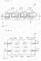
- Fig. 5 is a plan view showing a configuration of the laser light source unit 100B according to a third embodiment of the present invention.
- outlines of the laser oscillation elements 30a, 30b, 30c, 30d, 30e, 30f are indicated by dotted lines, and the fixing member 18 is not shown.
- the laser light source unit 100B is different from the laser light source unit 100 in Figs. 1 and 2 in that it includes a housing 10B in place of the housing 10, that it includes one electrode Eda in place of the two electrodes Eda, that it includes one electrode Edb in place of the two electrodes Edb, that it has regions Rg1B, Rg2B in place of the regions Rg1, Rg2, and that it further has a region Rg3.
- Other configurations of the laser light source unit 100B are similar to those of the laser light source unit 100, and thus, detailed descriptions thereof are not repeated.
- the housing 10B is different from the housing 10 in that two grooves V1b are provided in place of the four grooves V1b, and in that it further has a groove V1ax.
- Other configurations of the housing 10B are similar to those of the housing 10, and thus, detailed descriptions thereof are not repeated.
- internal configurations of the two grooves V1b in the housing 10B are similar to those of the grooves V1b of the housing 10 in Fig. 1 , and thus, detailed descriptions thereof are not repeated.
- internal configurations of the four grooves V1a in the housing 10B are similar to those of each of the grooves V1a of the housing 10 in Fig. 1 , and thus, detailed descriptions thereof are not repeated. That is, inside each of the grooves V1b, and inside each of the grooves V1a, the conductive layer 12 and the insulating layer 11 are provided as in Fig. 1 .
- the insulating layer 11 is a layer configured to insulate the housing 10B and the more than one electrodes 3 inserted into the groove VI.
- the insulating layer 11 of the groove V1a, into which the electrode 3b of the laser oscillation element 30a and the electrode 3a of the laser oscillation element 30b are inserted insulates between the housing 10B, and the electrode 3b of the laser oscillation element 30a and the electrode 3a of the laser oscillation element 30b.
- the n laser oscillation elements 30 of the laser light source unit 100B are fixed to the housing 10B by the fixing member 18, as shown in Fig. 1 .
- each of the n laser oscillation elements 30 is an element configured to drive, utilizing the electrode 3a and the electrode 3b.
- the n laser oscillation elements 30 (laser oscillation elements 30a, 30b, 30c, 30d, 30e, 30f) are electrically connected in series between the one electrode Eda and the one electrode Edb.
- the region Rg1B is different from the region Rg1 in Fig. 2 in that it includes the one groove V1b in place of the two grooves V1b. That is, in the region Rg1B, the one groove V1b and the two grooves V1a are provided.
- the laser oscillation elements 30a, 30b are fixed to the one groove V1b and the two grooves V1a in the region Rg1B as in Fig. 1 .
- the electrode 3a of the laser oscillation element 30a is inserted into the groove V1b of the region Rg1B.
- the electrode 3a of the laser oscillation element 30a is electrically connected to the one electrode Eda.
- the electrode 3b of the laser oscillation element 30a and the electrode 3a of the laser oscillation element 30b are inserted into the left groove V1a of the two grooves V1a. Note that the electrode 3b of the laser oscillation element 30a and the electrode 3a of the laser oscillation element 30b are electrically connected by the conductive layer 12.
- the region Rg3 includes the groove V1ax.
- a shape of the groove V1ax is a U shape as one example.
- the electrode 3b of the laser oscillation element 30c and the electrode 3a of the laser oscillation element 30d are inserted into the groove V1ax.
- the conductive layer 12 and the insulating layer 11 are provided as in the groove V1a.
- the conductive layer 12 of the groove V1ax electrically connects the two electrodes 3 inserted into the groove V1ax. That is, the conductive layer 12 of the groove V1ax electrically connects the electrode 3b of the laser oscillation element 30c and the electrode 3a of the laser oscillation element 30d.
- the region Rg2B is different from the region Rg2 in Fig. 2 in that it includes the one groove V1b in place of the two grooves V1b. That is, in the region Rg2B, the one groove V1b and the two grooves V1a are provided.
- the laser oscillation elements 30d, 30e, 30f electrically connected in series are fixed to the one groove V1b and the two grooves V1a in the region Rg2B.
- the electrode 3b of the laser oscillation element 30f is inserted into the groove V1b of the region Rg2B.
- the electrode 3b of the laser oscillation element 30f is electrically connected to the one electrode Edb in the region Rg2B.
- the electrode 3b of the laser oscillation element 30d and the electrode 3a of the laser oscillation element 30e are inserted into the right groove V1a of the two grooves V1a.
- the n laser oscillation elements 30 are electrically connected in series between the one electrode Eda and the one electrode Edb. That is, the use of the one electrode Eda and the one electrode Edb allows current to be supplied to the n laser oscillation elements 30 of the laser light source unit 100B. That is, only two terminals for supplying the current to the laser light source unit 100B from an outside are required.
- configuration CtBa a configuration in which the foregoing configuration CtA is applied to the configuration CtB of the present embodiment (hereinafter, also referred to as a "configuration CtBa") may be employed.
- the n laser oscillation elements 30 are joined to the housing 10B by solder (metal).
- the fixing member 18 is not used.
- each of the laser oscillation elements 30 is fixed to the housing 10B by solder (metal) and the fixing member 18.
- a configuration of the present embodiment is a configuration in which the functions of insulation, electrical conduction and the like can be added to a housing (hereinafter, referred to as a "configuration CtC").
- a laser light source unit to which the configuration CtC is applied is also referred to as a “laser light source unit 100C.”
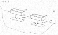
- Fig. 6 is a perspective view showing a part of the configuration of the laser light source unit 100C according to a fourth embodiment of the present invention.
- the laser light source unit 100C is different from the laser light source unit 100 in Fig. 1 in that it includes a housing 10N in place of the housing 10, and that it includes a plurality of parts 50.
- Other configurations of the laser light source unit 100C are similar to those of the laser light source unit 100, and thus, detailed descriptions thereof are not repeated.
- the housing 10N is different from the housing 10 in that inside of each of the grooves V1a, the conductive layer 12 and the insulating layer 11 do not exist. Other configurations and functions of the housing 10N are similar to those of the housing 10, and thus, detailed descriptions thereof are not repeated.
- the housing 10N is a part formed only by machining.
- Fig. 7 is cross-sectional views each showing the part 50 according to the third embodiment of the present invention.
- the part 50 has, for example, a configuration shown in Fig. 7(a) .
- a shape of the part 50 is a box shape having a bottom and no lid.
- the part 50 includes a member 51 and the conductive layer 12.
- a shape of the member 51 is a box shape having a bottom and no lid.
- the member 51 is made of an insulating material.
- the insulating material is, for example, plastic, silicon or the like.
- the conductive layer 12 is formed as shown in Fig. 7(a) .
- a configuration of the part 50 is not limited to the configuration in Fig. 7(a) .
- the configuration of the part 50 may be, for example, a configuration in Fig. 7(b) . That is, as shown in Fig. 7(b) , in the whole inside of the member 51 of the part 50, the conductive layer 12 may be formed.
- the part 50 is inserted into each of the grooves V1a of the housing 10N from an outside of the housing 10N.
- a state of the housing 10N where the part 50 is inserted into each of the grooves V1a of the housing 10N is also referred to as a "state St1."
- the member 51 and the conductive layer 12 exist in each of the grooves V1a of the housing 10N in the state St1.
- the conductive layer 12 existing in each of the grooves V1a of the housing 10N in the state St1 has been inserted into the groove V1a from the outside of the housing 10N.
- the member 51 is made of the insulating material. Therefore, the member 51 of the housing 10N in the state St1 functions as an insulating layer. That is, the member 51 as the insulating layer, which exists in each of the grooves V1a of the housing 10N in the state St1, has been inserted into the groove V1a from the outside of the housing 10N. Accordingly, the housing 10N in the state St1 has the conductive layer 12 and the insulating layer (member 51) as in the housing 10 of Fig. 1 .
- the n laser oscillation elements 30 are fixed to the housing 10N in the state St1 by the fixing member 18. Therefore, the conductive layer 12 and the insulating layer (member 51) existing in the housing ION in the state St1 have functions similar to those of the conductive layer 12 and the insulating layer 11 of the housing 10, respectively.
- the conductive layer 12 of the part 50 inserted into the groove V1a existing in the housing ION in the state St1 electrically connects the electrode 3b of the laser oscillation element 30a and the electrode 3a of the laser oscillation element 30b.
- the insulating layer (member 51) of the part 50 inserted into the groove V1a existing in the housing 10N in the state St1 insulates between the housing 10N, and the electrode 3b of the laser oscillation element 30a and the electrode 3a of the laser oscillation element 30b.
- the housing 10N is formed only by machining, and the part 50 has the functions of insulation and the electrical conduction. This makes the processing of the parts of the housing 10N and the like easy. Moreover, the configuration of the housing 10N itself can be simplified. This can suppress costs of the laser light source unit 100C.
- configuration CtCa a configuration in which the foregoing configuration CtA is applied to the configuration CtC of the present embodiment (hereinafter, also referred to as a "configuration CtCa") may be employed.
- the n laser oscillation elements 30 are joined to the housing 10N in the state St1 by solder (metal).
- the fixing member 18 is not used.
- each of the laser oscillation elements 30 is fixed to the housing ION in the state St1 by the fixing member 18.
- a configuration of the present modification is a configuration in which a material of the housing of the laser light source unit is metal excellent in heat conduction (hereinafter, also referred to as a "configuration CtX").
- the metal excellent in heat conduction is, for example, aluminum, copper, or the like.
- the configuration CtX can be applied to the configurations of the first to fourth embodiments.
- a configuration in which the configuration CtX is applied to the laser light source unit 100 of the first embodiment is also referred to as a "configuration Ctlx.”
- the housing 10 of the laser light source unit 100 in the configuration Ctlx is made of aluminum or copper.
- the heat generated by the laser oscillation elements 30 can be efficiently transmitted to the back surface 10b (cooling surface) of the housing 10. Therefore, the housing excellent in cooling performance can be realized. Accordingly, the heat transmitted to the back surface 10b (cooling surface) can be exhausted by the cooling apparatus not shown.
- a thickness Th1 of the housing 10 in Fig 1 is decided in view of a rigidity, an efficiency of the heat conduction, and the like of the housing 10.
- a thickness Th1 becomes larger, a heat resistance due to heat transmission increases, and the heat exhaust efficiency of the housing 10 decreases.
- the thickness Th1 becomes smaller the rigidity of the housing 10 decreases. In this case, an emission direction of a laser beam is not stable, and a utilization efficiency in an optical system not shown of the projection-type display apparatus decreases. Therefore, it is desirable that the thickness Th1 is about 3 millimeters to 5 millimeters.
- the housing 10 is made of the metal excellent in heat conduction. Therefore, the plurality of laser oscillation elements 30 can be efficiently cooled simultaneously.
- a configuration in which the configuration CtX is applied to the configuration CtA of the second embodiment is also referred to as a "configuration CtAx.”
- the housing 10 of the laser light source unit 100A in the configuration CtAx is made of aluminum or copper.
- the configuration CtX may be applied to the configuration CtNA of the second embodiment.
- a configuration in which the configuration CtX is applied to the configuration CtB of the third embodiment is also referred to as a "configuration CtBx.”
- the housing 10B of the laser light source unit 100B in the configuration CtBx is made of aluminum or copper.
- the configuration CtX may be applied to the configuration CtBa of the third embodiment.
- the configuration CtX may be applied to the configuration CtNBa of the third embodiment.
- a configuration in which the configuration CtX is applied to the configuration CtC of the fourth embodiment is also referred to as a "configuration CtCx.”
- the housing 10N of the laser light source unit 100C in the configuration CtCx is made of aluminum or copper.
- the configuration CtX may be applied to the configuration CtCa of the fourth embodiment.
- the configuration CtX may be applied to the configuration CtNCa of the fourth embodiment.
- the present invention is not limited only to the embodiments, and the modification described above. It should be noted that, within the scope of the present invention, the embodiments and the modification of the present invention may be freely combined, and/or may be appropriately modified or omitted.
- the arrangement state of the n laser oscillation elements 30 are not limited to, for example, the state in Fig.2 .
Landscapes
- Physics & Mathematics (AREA)
- Condensed Matter Physics & Semiconductors (AREA)
- General Physics & Mathematics (AREA)
- Electromagnetism (AREA)
- Optics & Photonics (AREA)
- Semiconductor Lasers (AREA)
- Projection Apparatus (AREA)
Applications Claiming Priority (1)
| Application Number | Priority Date | Filing Date | Title |
|---|---|---|---|
| PCT/JP2017/008723 WO2018163235A1 (fr) | 2017-03-06 | 2017-03-06 | Unité de source de lumière laser |
Publications (2)
| Publication Number | Publication Date |
|---|---|
| EP3595103A1 true EP3595103A1 (fr) | 2020-01-15 |
| EP3595103A4 EP3595103A4 (fr) | 2020-03-25 |
Family
ID=63448450
Family Applications (1)
| Application Number | Title | Priority Date | Filing Date |
|---|---|---|---|
| EP17899990.0A Withdrawn EP3595103A4 (fr) | 2017-03-06 | 2017-03-06 | Unité de source de lumière laser |
Country Status (6)
| Country | Link |
|---|---|
| US (1) | US10971899B2 (fr) |
| EP (1) | EP3595103A4 (fr) |
| JP (1) | JP6576592B2 (fr) |
| CN (1) | CN110352539B (fr) |
| CA (1) | CA3048726A1 (fr) |
| WO (1) | WO2018163235A1 (fr) |
Cited By (1)
| Publication number | Priority date | Publication date | Assignee | Title |
|---|---|---|---|---|
| US10985526B2 (en) * | 2016-11-25 | 2021-04-20 | Furukawa Electric Co., Ltd. | Laser device and light-source device |
Family Cites Families (13)
| Publication number | Priority date | Publication date | Assignee | Title |
|---|---|---|---|---|
| CA2284946A1 (fr) * | 1999-10-04 | 2001-04-04 | Institut National D'optique | Ensemble de reseaux de diodes laser fait d'un substrat monolithique nervure |
| US7016383B2 (en) * | 2003-08-27 | 2006-03-21 | Northrop Grumman Corporation | Immersion-cooled monolithic laser diode array and method of manufacturing the same |
| JP5505719B2 (ja) | 2010-06-28 | 2014-05-28 | カシオ計算機株式会社 | 光源装置及びプロジェクタ |
| US8198109B2 (en) * | 2010-08-27 | 2012-06-12 | Quarkstar Llc | Manufacturing methods for solid state light sheet or strip with LEDs connected in series for general illumination |
| JP2012156233A (ja) | 2011-01-25 | 2012-08-16 | Seiko Epson Corp | 光源装置及びプロジェクター |
| CN102361218B (zh) * | 2011-10-28 | 2013-02-06 | 中国科学院半导体研究所 | 半导体激光器二极管封装夹具 |
| DE102012213193B4 (de) * | 2012-07-26 | 2023-09-14 | Coretronic Corporation | Anordnung von optischen halbleiterelementen |
| US8804782B2 (en) * | 2012-10-29 | 2014-08-12 | Coherent, Inc. | Macro-channel water-cooled heat-sink for diode-laser bars |
| DE102013224420A1 (de) * | 2013-05-13 | 2014-11-13 | Osram Gmbh | Laserbauelement und Verfahren zur seiner Herstellung |
| JP6272067B2 (ja) * | 2014-02-13 | 2018-01-31 | 三菱電機株式会社 | レーザ光源モジュールおよびレーザ光源装置 |
| JP6500223B2 (ja) * | 2014-04-17 | 2019-04-17 | パナソニックIpマネジメント株式会社 | 光源装置および投写型映像表示装置 |
| JP6492462B2 (ja) * | 2014-08-29 | 2019-04-03 | 日亜化学工業株式会社 | 光源装置 |
| CN105703215B (zh) * | 2016-04-08 | 2019-02-05 | 无锡亮源激光技术有限公司 | 一种用于固体激光器泵浦源的半导体激光器 |
-
2017
- 2017-03-06 EP EP17899990.0A patent/EP3595103A4/fr not_active Withdrawn
- 2017-03-06 CA CA3048726A patent/CA3048726A1/fr not_active Abandoned
- 2017-03-06 CN CN201780087659.7A patent/CN110352539B/zh not_active Expired - Fee Related
- 2017-03-06 JP JP2019503827A patent/JP6576592B2/ja not_active Expired - Fee Related
- 2017-03-06 WO PCT/JP2017/008723 patent/WO2018163235A1/fr not_active Ceased
- 2017-03-06 US US16/476,206 patent/US10971899B2/en not_active Expired - Fee Related
Cited By (1)
| Publication number | Priority date | Publication date | Assignee | Title |
|---|---|---|---|---|
| US10985526B2 (en) * | 2016-11-25 | 2021-04-20 | Furukawa Electric Co., Ltd. | Laser device and light-source device |
Also Published As
| Publication number | Publication date |
|---|---|
| US20200388992A1 (en) | 2020-12-10 |
| CN110352539B (zh) | 2020-12-25 |
| JPWO2018163235A1 (ja) | 2019-06-27 |
| EP3595103A4 (fr) | 2020-03-25 |
| JP6576592B2 (ja) | 2019-09-18 |
| CN110352539A (zh) | 2019-10-18 |
| CA3048726A1 (fr) | 2018-09-13 |
| WO2018163235A1 (fr) | 2018-09-13 |
| US10971899B2 (en) | 2021-04-06 |
Similar Documents
| Publication | Publication Date | Title |
|---|---|---|
| CN113422280B (zh) | 具有激光阵列照明的系统和装置 | |
| WO2018116634A1 (fr) | Module optique | |
| WO2006126645A1 (fr) | Embase pour pièce électronique | |
| US10707643B2 (en) | Laser light source module | |
| KR101246887B1 (ko) | 방송용 조명장치 | |
| CN105972533A (zh) | 光源模块 | |
| CN102889489A (zh) | 灯条结构及光源装置 | |
| EP3098864A1 (fr) | Module de conversion thermoélectrique | |
| US9276376B2 (en) | Laser module | |
| JP6303952B2 (ja) | 基板実装構造及び電源装置 | |
| EP3595103A1 (fr) | Unité de source de lumière laser | |
| JP2015050164A (ja) | 電池モジュール | |
| JP2013016810A (ja) | 放熱装置 | |
| CN106233069A (zh) | 固持座以及具有固持座的led系统 | |
| WO2013179374A1 (fr) | Dispositif à semi-conducteur | |
| CN205122574U (zh) | 基板装置以及电子设备 | |
| JP2005086094A (ja) | レーザダイオードモジュール | |
| KR101291110B1 (ko) | Led 칩 패키지 | |
| JP2005142520A (ja) | パワーモジュール | |
| CN216251620U (zh) | 一种多波长cos阵列激光器 | |
| KR101058097B1 (ko) | 광학 모듈, 이를 갖는 백라이트 어셈블리 및 이를 갖는표시장치 | |
| CN220400161U (zh) | 显示模组和电子设备 | |
| JP2014138095A (ja) | 発光ユニット及び照明器具 | |
| JP2008053380A (ja) | レーザ装置 | |
| JP6811912B1 (ja) | レーザ光源装置およびレーザ光源装置の製造方法 |
Legal Events
| Date | Code | Title | Description |
|---|---|---|---|
| PUAI | Public reference made under article 153(3) epc to a published international application that has entered the european phase |
Free format text: ORIGINAL CODE: 0009012 |
|
| 17P | Request for examination filed |
Effective date: 20190809 |
|
| AK | Designated contracting states |
Kind code of ref document: A1 Designated state(s): AL AT BE BG CH CY CZ DE DK EE ES FI FR GB GR HR HU IE IS IT LI LT LU LV MC MK MT NL NO PL PT RO RS SE SI SK SM TR |
|
| AX | Request for extension of the european patent |
Extension state: BA ME |
|
| A4 | Supplementary search report drawn up and despatched |
Effective date: 20200220 |
|
| RIC1 | Information provided on ipc code assigned before grant |
Ipc: H01S 5/042 20060101ALI20200215BHEP Ipc: H01S 5/022 20060101AFI20200215BHEP Ipc: H01S 5/02 20060101ALI20200215BHEP Ipc: H01S 5/40 20060101ALI20200215BHEP Ipc: H01S 5/024 20060101ALN20200215BHEP |
|
| DAV | Request for validation of the european patent (deleted) | ||
| DAX | Request for extension of the european patent (deleted) | ||
| STAA | Information on the status of an ep patent application or granted ep patent |
Free format text: STATUS: THE APPLICATION HAS BEEN WITHDRAWN |
|
| 18W | Application withdrawn |
Effective date: 20210105 |