EP3597794A1 - Metallplatte, abscheidungsmaske und herstellungsverfahren dafür - Google Patents
Metallplatte, abscheidungsmaske und herstellungsverfahren dafür Download PDFInfo
- Publication number
- EP3597794A1 EP3597794A1 EP18767292.8A EP18767292A EP3597794A1 EP 3597794 A1 EP3597794 A1 EP 3597794A1 EP 18767292 A EP18767292 A EP 18767292A EP 3597794 A1 EP3597794 A1 EP 3597794A1
- Authority
- EP
- European Patent Office
- Prior art keywords
- nickel
- metal plate
- iron
- plating layer
- thickness
- Prior art date
- Legal status (The legal status is an assumption and is not a legal conclusion. Google has not performed a legal analysis and makes no representation as to the accuracy of the status listed.)
- Granted
Links
Images


Classifications
-
- C—CHEMISTRY; METALLURGY
- C23—COATING METALLIC MATERIAL; COATING MATERIAL WITH METALLIC MATERIAL; CHEMICAL SURFACE TREATMENT; DIFFUSION TREATMENT OF METALLIC MATERIAL; COATING BY VACUUM EVAPORATION, BY SPUTTERING, BY ION IMPLANTATION OR BY CHEMICAL VAPOUR DEPOSITION, IN GENERAL; INHIBITING CORROSION OF METALLIC MATERIAL OR INCRUSTATION IN GENERAL
- C23F—NON-MECHANICAL REMOVAL OF METALLIC MATERIAL FROM SURFACE; INHIBITING CORROSION OF METALLIC MATERIAL OR INCRUSTATION IN GENERAL; MULTI-STEP PROCESSES FOR SURFACE TREATMENT OF METALLIC MATERIAL INVOLVING AT LEAST ONE PROCESS PROVIDED FOR IN CLASS C23 AND AT LEAST ONE PROCESS COVERED BY SUBCLASS C21D OR C22F OR CLASS C25
- C23F1/00—Etching metallic material by chemical means
- C23F1/10—Etching compositions
- C23F1/14—Aqueous compositions
- C23F1/16—Acidic compositions
- C23F1/28—Acidic compositions for etching iron group metals
-
- C—CHEMISTRY; METALLURGY
- C25—ELECTROLYTIC OR ELECTROPHORETIC PROCESSES; APPARATUS THEREFOR
- C25D—PROCESSES FOR THE ELECTROLYTIC OR ELECTROPHORETIC PRODUCTION OF COATINGS; ELECTROFORMING; APPARATUS THEREFOR
- C25D5/00—Electroplating characterised by the process; Pretreatment or after-treatment of workpieces
- C25D5/10—Electroplating with more than one layer of the same or of different metals
- C25D5/12—Electroplating with more than one layer of the same or of different metals at least one layer being of nickel or chromium
-
- B—PERFORMING OPERATIONS; TRANSPORTING
- B32—LAYERED PRODUCTS
- B32B—LAYERED PRODUCTS, i.e. PRODUCTS BUILT-UP OF STRATA OF FLAT OR NON-FLAT, e.g. CELLULAR OR HONEYCOMB, FORM
- B32B15/00—Layered products comprising a layer of metal
- B32B15/01—Layered products comprising a layer of metal all layers being exclusively metallic
- B32B15/013—Layered products comprising a layer of metal all layers being exclusively metallic one layer being formed of an iron alloy or steel, another layer being formed of a metal other than iron or aluminium
- B32B15/015—Layered products comprising a layer of metal all layers being exclusively metallic one layer being formed of an iron alloy or steel, another layer being formed of a metal other than iron or aluminium the said other metal being copper or nickel or an alloy thereof
-
- C—CHEMISTRY; METALLURGY
- C22—METALLURGY; FERROUS OR NON-FERROUS ALLOYS; TREATMENT OF ALLOYS OR NON-FERROUS METALS
- C22C—ALLOYS
- C22C38/00—Ferrous alloys, e.g. steel alloys
- C22C38/08—Ferrous alloys, e.g. steel alloys containing nickel
-
- C—CHEMISTRY; METALLURGY
- C23—COATING METALLIC MATERIAL; COATING MATERIAL WITH METALLIC MATERIAL; CHEMICAL SURFACE TREATMENT; DIFFUSION TREATMENT OF METALLIC MATERIAL; COATING BY VACUUM EVAPORATION, BY SPUTTERING, BY ION IMPLANTATION OR BY CHEMICAL VAPOUR DEPOSITION, IN GENERAL; INHIBITING CORROSION OF METALLIC MATERIAL OR INCRUSTATION IN GENERAL
- C23C—COATING METALLIC MATERIAL; COATING MATERIAL WITH METALLIC MATERIAL; SURFACE TREATMENT OF METALLIC MATERIAL BY DIFFUSION INTO THE SURFACE, BY CHEMICAL CONVERSION OR SUBSTITUTION; COATING BY VACUUM EVAPORATION, BY SPUTTERING, BY ION IMPLANTATION OR BY CHEMICAL VAPOUR DEPOSITION, IN GENERAL
- C23C14/00—Coating by vacuum evaporation, by sputtering or by ion implantation of the coating forming material
- C23C14/04—Coating on selected surface areas, e.g. using masks
- C23C14/042—Coating on selected surface areas, e.g. using masks using masks
-
- C—CHEMISTRY; METALLURGY
- C23—COATING METALLIC MATERIAL; COATING MATERIAL WITH METALLIC MATERIAL; CHEMICAL SURFACE TREATMENT; DIFFUSION TREATMENT OF METALLIC MATERIAL; COATING BY VACUUM EVAPORATION, BY SPUTTERING, BY ION IMPLANTATION OR BY CHEMICAL VAPOUR DEPOSITION, IN GENERAL; INHIBITING CORROSION OF METALLIC MATERIAL OR INCRUSTATION IN GENERAL
- C23F—NON-MECHANICAL REMOVAL OF METALLIC MATERIAL FROM SURFACE; INHIBITING CORROSION OF METALLIC MATERIAL OR INCRUSTATION IN GENERAL; MULTI-STEP PROCESSES FOR SURFACE TREATMENT OF METALLIC MATERIAL INVOLVING AT LEAST ONE PROCESS PROVIDED FOR IN CLASS C23 AND AT LEAST ONE PROCESS COVERED BY SUBCLASS C21D OR C22F OR CLASS C25
- C23F1/00—Etching metallic material by chemical means
- C23F1/02—Local etching
- C23F1/04—Chemical milling
-
- C—CHEMISTRY; METALLURGY
- C25—ELECTROLYTIC OR ELECTROPHORETIC PROCESSES; APPARATUS THEREFOR
- C25D—PROCESSES FOR THE ELECTROLYTIC OR ELECTROPHORETIC PRODUCTION OF COATINGS; ELECTROFORMING; APPARATUS THEREFOR
- C25D5/00—Electroplating characterised by the process; Pretreatment or after-treatment of workpieces
- C25D5/48—After-treatment of electroplated surfaces
- C25D5/50—After-treatment of electroplated surfaces by heat-treatment
-
- C—CHEMISTRY; METALLURGY
- C25—ELECTROLYTIC OR ELECTROPHORETIC PROCESSES; APPARATUS THEREFOR
- C25D—PROCESSES FOR THE ELECTROLYTIC OR ELECTROPHORETIC PRODUCTION OF COATINGS; ELECTROFORMING; APPARATUS THEREFOR
- C25D7/00—Electroplating characterised by the article coated
-
- C—CHEMISTRY; METALLURGY
- C25—ELECTROLYTIC OR ELECTROPHORETIC PROCESSES; APPARATUS THEREFOR
- C25D—PROCESSES FOR THE ELECTROLYTIC OR ELECTROPHORETIC PRODUCTION OF COATINGS; ELECTROFORMING; APPARATUS THEREFOR
- C25D7/00—Electroplating characterised by the article coated
- C25D7/06—Wires; Strips; Foils
- C25D7/0614—Strips or foils
-
- H—ELECTRICITY
- H10—SEMICONDUCTOR DEVICES; ELECTRIC SOLID-STATE DEVICES NOT OTHERWISE PROVIDED FOR
- H10K—ORGANIC ELECTRIC SOLID-STATE DEVICES
- H10K71/00—Manufacture or treatment specially adapted for the organic devices covered by this subclass
-
- H—ELECTRICITY
- H10—SEMICONDUCTOR DEVICES; ELECTRIC SOLID-STATE DEVICES NOT OTHERWISE PROVIDED FOR
- H10K—ORGANIC ELECTRIC SOLID-STATE DEVICES
- H10K71/00—Manufacture or treatment specially adapted for the organic devices covered by this subclass
- H10K71/10—Deposition of organic active material
- H10K71/16—Deposition of organic active material using physical vapour deposition [PVD], e.g. vacuum deposition or sputtering
- H10K71/166—Deposition of organic active material using physical vapour deposition [PVD], e.g. vacuum deposition or sputtering using selective deposition, e.g. using a mask
-
- C—CHEMISTRY; METALLURGY
- C23—COATING METALLIC MATERIAL; COATING MATERIAL WITH METALLIC MATERIAL; CHEMICAL SURFACE TREATMENT; DIFFUSION TREATMENT OF METALLIC MATERIAL; COATING BY VACUUM EVAPORATION, BY SPUTTERING, BY ION IMPLANTATION OR BY CHEMICAL VAPOUR DEPOSITION, IN GENERAL; INHIBITING CORROSION OF METALLIC MATERIAL OR INCRUSTATION IN GENERAL
- C23C—COATING METALLIC MATERIAL; COATING MATERIAL WITH METALLIC MATERIAL; SURFACE TREATMENT OF METALLIC MATERIAL BY DIFFUSION INTO THE SURFACE, BY CHEMICAL CONVERSION OR SUBSTITUTION; COATING BY VACUUM EVAPORATION, BY SPUTTERING, BY ION IMPLANTATION OR BY CHEMICAL VAPOUR DEPOSITION, IN GENERAL
- C23C14/00—Coating by vacuum evaporation, by sputtering or by ion implantation of the coating forming material
- C23C14/06—Coating by vacuum evaporation, by sputtering or by ion implantation of the coating forming material characterised by the coating material
- C23C14/12—Organic material
-
- Y—GENERAL TAGGING OF NEW TECHNOLOGICAL DEVELOPMENTS; GENERAL TAGGING OF CROSS-SECTIONAL TECHNOLOGIES SPANNING OVER SEVERAL SECTIONS OF THE IPC; TECHNICAL SUBJECTS COVERED BY FORMER USPC CROSS-REFERENCE ART COLLECTIONS [XRACs] AND DIGESTS
- Y02—TECHNOLOGIES OR APPLICATIONS FOR MITIGATION OR ADAPTATION AGAINST CLIMATE CHANGE
- Y02E—REDUCTION OF GREENHOUSE GAS [GHG] EMISSIONS, RELATED TO ENERGY GENERATION, TRANSMISSION OR DISTRIBUTION
- Y02E60/00—Enabling technologies; Technologies with a potential or indirect contribution to GHG emissions mitigation
- Y02E60/10—Energy storage using batteries
Definitions
- An embodiment relates to a metal plate. Specifically, an embodiment relates to a metal plate capable of being used for a mask for deposition. More specifically, an organic light emitting diode (OLED) panel may be manufactured by using the mask for deposition according to an embodiment.
- OLED organic light emitting diode
- various display devices such as a liquid crystal display device and an electroluminescent display device have been developed.
- the electroluminescent display device has been spotlighted as a next generation display device due to excellent characteristics such as low light emission, low power consumption, and high resolution, and the like, as compared with the liquid crystal display device.
- an organic light emitting display device and an inorganic light emitting display device in an electric field display device there are an organic light emitting display device and an inorganic light emitting display device in an electric field display device. That is, an electric field display device may be classified into the organic light emitting display device and the inorganic light emitting display device according to a material of a light emitting layer.
- the organic light emitting display device has received attention because the organic light emitting display device has a wide viewing angle, has a fast response speed, and is required to have low power consumption.
- An organic material constituting such a light emitting layer may be formed to have a pattern for forming a pixel on a substrate by a fine metal mask method.
- the fine metal mask that is, a mask for deposition may have a through-hole corresponding to the pattern to be formed on the substrate, and, patterns of red (R), green (G), and blue (B) forming a pixel may be formed by depositing the organic material after the fine metal mask is aligned on the substrate.
- a rolled metal plate has a problem that it is difficult to be manufactured with a thin thickness. In case of manufacturing the rolled metal plate at 20 ⁇ m or less, there is a problem that it is difficult to form through-holes of uniform size as quality of a product is lowered.
- a metal plate formed by plating may have a thin thickness
- when a metal plate is made of an alloy there is a problem that it is difficult to control the composition thereof.
- a metal plate formed with a sub-micro unit thickness on an initial plating layer having a constant alloy ratio may have the same alloy ratio as the initial plating layer, but a micro unit thickness metal plate has a difficult problem of having the same alloy ratio as the initial plating layer. Accordingly, the plated metal plate having a thickness of 1 ⁇ m or more has a problem that the quality of the product is lowered due to an increase in thermal expansion coefficient.
- a metal plate for a deposition mask having a new structure, a deposition mask, and a method of manufacturing thereof are required.
- An embodiment is directed to providing a metal plate capable of ensuring uniformity of an alloy composition while having a small thickness.
- an embodiment is directed to providing a metal plate capable of forming uniform through-holes.
- a multi-layered metal plate has a thickness of 30 ⁇ m or less and includes an alloy of nickel (Ni) and iron (Fe), a first outer portion occupying a region of 20% or less of the total thickness from one surface of the metal plate, a second outer portion occupying a region of 20% or less of the total thickness from the other surface opposite to the one surface, and a central portion other than the first outer portion and the second outer portion, wherein nickel contents of the first outer portion and the second outer portion are greater than that of the central portion.
- Ni nickel
- Fe iron
- a multi-layered metal plate including an alloy of nickel (Ni) and iron (Fe) includes: forming a nickel plating layer; forming an iron plating layer on the nickel plating layer; forming a multi-layered plating plate by alternately repeating the nickel plating layer and the iron plating layer to be disposed thereon; and heat-treating the multi-layered plating plate at a temperature of 300°C or higher.
- a multi-layered metal plate according to an embodiment has a thickness of 30 ⁇ m or less, includes an alloy of nickel (Ni) and iron (Fe), and includes an outer portion occupying a region of 20% or less of the total thickness and a central portion other than the outer portion, and a nickel content of the outer portion may be greater than that of the central portion. Accordingly, in the multi-layered metal plate according to the embodiment, an etch rate on a surface in which the outer portion is position may be delayed, thereby improving an etching factor.
- the multi-layered metal plate including an alloy of nickel (Ni) and iron (Fe) according to the embodiment may formed by plating. Accordingly, the multi-layered metal plate according to the embodiment may be formed with a thin thickness of 30 ⁇ m or less.
- a manufacturing method of the multi-layered metal plate according to the embodiment may include: forming a nickel plating layer; forming an iron plating layer on the nickel plating layer; forming a multi-layered plating plate by alternately repeating the nickel plating layer and the iron plating layer to be disposed thereon; and heat-treating the multi-layered plating plate at a temperature of 300°C or higher.
- the metal plate according to the embodiment may be formed as a multi-layered metal plate by heat treatment after being formed such that the nickel plating layer and the iron plating layer are alternately disposed.
- iron in the iron plating layer and nickel in the nickel plating layer may be diffused respectively by heat treatment at a temperature of 300°C or higher, thereby having a uniform content in a predetermined thickness range.
- the metal plate according to the embodiment may have a low thermal expansion coefficient, and a mask for deposition using the same may include uniform through-holes.
- each layer (film), region, pattern or structure may be modified for clarity and convenience of explanation, and thus does not entirely reflect the actual size.
- each layer (film), region pattern or structure in the case in which each layer (film), region pattern or structure is described as being formed “over”, “on” or “under” a substrate, each layer (film), area, pad or pattern, the "over”, “on” and “under” include both of forming “directly” and “indirectly”.
- Each embodiment may be implemented independently or together, and some elements may be excluded in order to meet objectives of the invention.
- embodiments will be described with reference to the accompanying drawings.
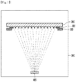
- FIGS. 1 and 2 A process for depositing an organic material on a substrate will be described with reference to FIGS. 1 and 2 .
- FIG. 1 is a view illustrating an organic material deposition apparatus in which a metal plate 100 according to an embodiment is included as a mask for deposition.
- the organic material deposition apparatus may include a metal plate 100 used as a mask for deposition, a mask frame 200, a substrate 300, an organic material deposition container 400, and a vacuum chamber 500.
- the mask for deposition may be a metal plate 100 according to an embodiment.
- the metal plate 100 may include a plurality of through-holes. At this point, the through-holes may be formed to correspond to patterns to be formed on the substrate.
- the mask frame 200 may include an opening.
- the plurality of through-holes of the metal plate 100 may be disposed on a region corresponding to the opening. Accordingly, organic material supplied to the organic material deposition container 400 may be deposited on the substrate 300.
- the mask for deposition may be disposed and fixed on the mask frame 200.
- the mask for deposition may be tensioned and fixed on the mask frame 200 by welding.
- the substrate 300 may be a substrate used for manufacturing a display device. Patterns of red (R), green (G), and blue (B) may be formed on the substrate 300 to form a pixel that is three primary colors of light.
- the organic material deposition container 400 may be a crucible. An organic material may be disposed at an inside of the crucible.
- the organic material may be deposited on the substrate 100.
- FIG. 2 is an enlarged view of one through-hole of the metal plate 100.
- the metal plate 100 may include a first surface 101 and a second surface 102 facing the first surface.
- the first surface 101 of the metal plate 100 may include a first surface hole V1 and the second surface 102 of the metal plate 100 may include a second surface hole V2.
- the through-hole may be formed by a connecting part CA through which the first surface hole V1 and the second surface hole V2 communicate with each other.
- a width of the second surface hole V2 may be greater than that of the first surface hole V1. At this point, the width of the first surface hole V1 may be measured at the first surface 101, and the width of the second surface hole V2 may be measured at the second surface 102.
- the first surface hole V1 may be disposed toward the substrate 300. Accordingly, the first surface hole V1 may have a shape corresponding to a deposition material D, that is, a pattern.
- the second surface hole V2 may be disposed toward the organic material deposition container 400. Accordingly, the second surface hole V2 may accommodate the organic material supplied from the organic material deposition container 400 in a wide width, and a fine pattern may be formed quickly on the substrate 300 through the first surface hole V1 having a width smaller than that of the second surface hole V2.
- FIGS. 3 and 4 are views illustrating a front view of a metal plate 100.
- the metal plate 100 may include a plurality of through-holes.
- the plurality of through-holes shown in FIG. 3 may represent the second surface hole V2.
- deviation of the diameter Cx in the horizontal direction and the diameter Cy in the vertical direction between holes (six holes in total as shown in the drawing) adjacent to the reference hole may be implemented at 2% to 10%, respectively. That is, when a size deviation between adjacent holes of one reference hole is implemented at 2% to 10%, uniformity of the deposition may be ensured.
- the size deviation between the reference hole and the adjacent holes may be 4% to 9%.
- the size deviation between the reference hole and the adjacent holes may be 5% to 7%.
- an occurrence rate of moire in an OLED panel after deposition may be increased.
- an occurrence rate of color stain in the OLED panel after deposition may be increased.
- An embodiment may be implemented at a size deviation within ⁇ 3 ⁇ m between the reference hole and the adjacent holes. Accordingly, deposition efficiency may be improved.
- the through-holes may be disposed in a row in a vertical axis and in a row in a horizontal axis.
- the through-holes may be disposed in a row in the vertical axis and may be disposed to be staggered from each other in the horizontal axis.
- the through-hole may have a first diameter measured in the vertical direction and a second diameter measured in the horizontal direction, which may correspond to each other or may be different from each other.
- the through-hole may have a third diameter measured in a first diagonal direction corresponding to a cross-sectional direction of A-A'and a fourth diameter measured in a second diagonal direction intersecting the first diagonal direction, which may be correspond to each other or may be different from each other.
- the through-hole may be rounded.
- FIG. 5 is an enlarged view of a cross section of a plurality of through-holes in a mask for deposition according to an embodiment.
- the metal plate 100 used for manufacturing a mask for deposition may include a central portion 101 and outer portions 102 and 103.
- the outer portions 102 and 103 may be located in a region of 20% or less of the total thickness.
- the outer portions 102 and 103 may be formed on one surface or both surfaces of the surface of the metal plate 100.
- the first outer portion 102 may be included on one surface of the metal plate 100 and the second outer portion 103 may be included on the other surface opposite to the one surface of the metal plate 100.
- the central portion 101 may refer to a metal plate portion other than the outer portions.
- the central portion 101 may be a region of a metal plate other than the first outer portion 102 and the second outer portion 103.
- the central portion 101 may be located at a central portion between the first outer portion 102 and the second outer portion 103.
- a total thickness TA of the metal plate 100 may be 30 ⁇ m or less.
- the total thickness TA of the metal plate 100 may be 25 ⁇ m or less.
- the total thickness TA of the metal plate 100 may be 1 ⁇ m to 20 ⁇ m or less.
- the metal plate 100 may be formed by a process other than rolling, and even when the metal plate 100 has a thickness of 20 ⁇ m or less, a manufacturing yield may be excellent.
- a multi-layered metal plate according to an embodiment may include a plurality of plating layers. Accordingly, the metal plate 100 may have a uniform content of nickel and iron even when the metal plate 100 is formed by plating to a thickness of 1 ⁇ m or more.
- the total thickness of at least one of the first outer portion 102 and the second outer portion 103 may be 5 ⁇ m or less.
- the first outer portion 102 may be defined as a thickness range of 5 ⁇ m or less from one surface of the metal plate
- the second outer portion 103 may be defined as a thickness range of 5 ⁇ m or less from the other surface of the metal plate.
- the total thickness of at least one of the first outer portion 102 and the second outer portion 103 may be 0 ⁇ m to 3 ⁇ m or less.
- the thicknesses of the first outer portion 102 and the second outer portion 103 may correspond to each other.
- the "corresponding" may be the same or may include an error due to tolerance.
- a thickness of the central portion 101 may be greater than that of the outer portions 102 and 103.
- the thickness of the central portion 101 may be greater than that of any outer portion of the first outer portion 102 and the second outer portion 103.
- the thickness of the central portion 101 may be greater than that of the first outer portion 102 and the second outer portion 103.
- the metal plate 100 may include an alloy of nickel (Ni) and iron (Fe).
- the central portion 101 and the outer portions 102 and 103 may include the alloy of nickel (Ni) and iron (Fe).
- a content of nickel in the outer portions 102 and 103 may be different from a content of nickel in the central portion 101.
- the content of nickel in the outer portions 102 and 103 may be larger than that of nickel in the central portion 101.
- a surface of the metal plate on which the outer portion is located may have an etch rate lower than that of the central portion to form through-holes. Accordingly, the multi-layered metal plate of the embodiment may improve an etching factor and may uniformly form the through-holes of a fine size.
- an iron content of the outer portions 102 and 103 may be different from that of the central portion 101.
- the iron content of the outer portions 102 and 103 may be smaller than that of the central portion 101.
- the content of nickel in the outer portions 102 and 103 may be 36 wt% to 100 wt%.
- the content of nickel in the outer portions 102 and 103 may be 40 wt% to 100 wt%.
- the nickel content of the outer portions 102 and 103 may be 50 wt% to 100 wt%.
- the central portion 101 may be a binary alloy having a predetermined content.
- the central portion 101 may be invar including about 36 wt% of nickel and about 64 wt% of iron.
- "36 wt%” and “64 wt%” may each include an error range of ⁇ 0.1 %, or an error range of ⁇ 0.01%.
- An invar-based metal plate may have a low thermal expansion coefficient. Such an invar characteristic may improve manufacturing efficiency and the manufacturing yield of the mask for deposition.
- the central portion 101 may have a uniform composition regardless of a measurement position or a measurement thickness.
- a content measured at any first point may be 36 wt% of nickel and 64 wt% of iron
- a content measured at any second point other than the first point may be 36 wt% of nickel and 64 wt% of iron.
- a content measured at any first thickness may be 36 wt% of nickel and 64 wt% of iron
- a content measured at any second thickness other than the first thickness may be 36 wt% of nickel and 64 wt% of iron.
- the central portion 101 of the multi-layered metal plate according to the embodiment may have a characteristic of low thermal expansion coefficient of invar. Accordingly, in the multi-layered metal plate according to the embodiment, the manufacturing efficiency of the mask for deposition including a plurality of fine through- holes having a uniform size may be excellent.
- the component, the content, and the weight % of the metal plate 100 may be confirmed using a method of examining the wt% of each component by selecting a specific region a ⁇ b on a plane of the metal plate 100, sampling a test piece (a ⁇ b ⁇ t) corresponding to the thickness t of the metal plate 100, and dissolving it in a strong acid, etc.
- the embodiment is not limited thereto, and the content may be confirmed by various methods.
- the metal plate 100 may have different widths of through-holes along the thickness direction of the through-hole.
- a width W1 of the first surface hole V1 may be greater than a width W3 of the connecting part CA.
- the width of the through-hole may be reduced as the first surface hole V1 goes from the first surface 101 toward the connecting part CA. More specifically, the width of the through-hole may be gradually reduced as the first surface hole V1 goes from the first surface 101 toward the connecting part CA.
- a width W2 of the second surface hole V2 may be greater than the width W3 of the connecting part CA.
- the width of the through-hole may be reduced as the second surface hole V2 goes from the second surface 102 toward the connecting part CA. More specifically, the width of the through-hole may be gradually reduced as the second surface hole V2 goes from the second surface 102 toward the connecting part CA.
- the deposition mask according to the embodiment may include a plurality of through holes.
- a width of one through hole may be 40 ⁇ m or less.
- the width of the through hole may be 5 ⁇ m to 40 ⁇ m.
- the width of the through hole may be 10 ⁇ m to 35 ⁇ m.
- at least one of the width W1 of the first surface hole and the width W2 of the second surface hole may have a width of 40 ⁇ m or less. When the width of the through hole exceeds 40 ⁇ m, it may be difficult to form a fine deposition pattern.
- a height H2 of the second surface hole V2 may be greater than a height H1 of the first surface hole V1.
- the height H1 of the first surface hole V1 may have a ratio of 1:3 to 30 to the thickness T of the metal plate 100.
- the height H1 of the first surface hole V1 may have a ratio of 1:3.5 to 12.5 with respect to the thickness T of the metal plate 100.
- the height H1 of the first surface hole V1 may have a ratio of 1:4.5 to 10.5 in relation to the thickness T of the metal plate 100.
- the height H1 of the first surface hole V1 is more than the ratio in relation to the thickness T of the metal plate 100, the height H1 of the first surface hole V1 is increased and the thickness variation of an organic material is increased and thus, a region in which an organic material is not deposited may occur. Accordingly, a manufacturing yield of the OLED panel manufactured through the mask for deposition may be reduced.
- the height H1 of the first surface hole V1 may be 0.1 to 7 ⁇ m.
- the height H1 of the first surface hole V1 may be 1 to 6 ⁇ m.
- the height H1 of the first surface hole V1 may be 2 to 4.5 ⁇ m.
- the height H1 of the first surface hole V1 is less than 0.1 ⁇ m, deposition efficiency of the organic material via the metal plate may be reduced.
- the height H1 of the first surface hole V1 is more than 7 ⁇ m, it is difficult to form a pattern of a fine size and a region in which an organic material is not deposited may occur, and thus the yield of the OLED panel manufactured through the same may be deteriorated.
- a third surface hole V3 adjacent to the first surface hole V1 and formed on the first surface 101 communicates with a fourth surface hole V4 adjacent to the second surface hole V1 and formed on the second surface 102, through the connecting part CA respectively, a plurality of through-holes may be formed.
- a substrate for a deposition mask may include bridge regions between an arbitrary first through-hole and a second through-hole adjacent to the first through-hole.
- the first surface 101 between the first surface hole V1 and the third surface hole V3 may include a first bridge region
- the second surface 102 between the second surface hole V1 and the fourth surface hole V4 may include a second bridge region
- the first bridge region may be larger than a planar area of the second bridge region.
- the bridge region may support the plurality of through holes so as to be spaced apart at a predetermined distance.
- An inclination angle connecting an arbitrary point A1 of an end of the connecting part CAto an arbitrary point B1 of an end of the second surface hole V2 may be in the range of 20 to 70 degrees.
- the inclination angle connecting an arbitrary point A1 of an end of the connecting part CAto an arbitrary point B1 of an end of the second surface hole V2 may be in the range of 30 to 60 degrees.
- the inclination angle connecting an arbitrary point A1 of an end of the connecting part CA to an arbitrary point B1 of an end of the second surface hole V2 may be in the range of 32 to 38 degrees or 52 to 58 degrees.
- the inclination angle connecting an arbitrary point A1 of an end of the connecting part CAto an arbitrary point B1 of an end of the second surface hole V2 is in the range of 20 to 70 degrees, uniformity of the deposition may be improved.
- the inclination angle is out of the range, a region in which an organic material is not deposited may occur, and thus deposition efficiency and process efficiency may be deteriorated.
- the width of the through-hole may become narrower as the first surface hole V1 goes toward a center of the metal plate 100.
- an inner surface of the first surface hole V1 may be a structure having curvature.
- the width of the through-hole may become narrower as the second surface hole V2 goes toward the center of the metal plate 100.
- the inner surface of the first surface hole V1 may be a structure having curvature. Accordingly, an introduction density of the deposition material may be controlled, and uniformity of the deposition may be improved as compared with a simple slope structure.
- a difference W1-W3 between the width W1 of the first surface hole V1 and the width W3 of the connecting part CA may be in the range of 0.2 to 14 ⁇ m.
- a vertical distance from an arbitrary point C1 at an end of the first surface hole V1 to an arbitrary point A1 at an end of the connecting part CA may be in the range of 0.1 to 7 ⁇ m.
- the vertical distance from an arbitrary point C1 at an end of the first surface hole V1 to an arbitrary point A1 at an end of the connecting part CA may be in the range of 1 to 6 ⁇ m.
- the vertical distance from an arbitrary point C1 at an end of the first surface hole V1 to an arbitrary point A1 at an end of the connecting part CA may be in the range of 2 to 4.5 ⁇ m.
- the vertical distance is less than 0.1 ⁇ m, deposition efficiency of the organic material via the metal plate 100 may be reduced.
- the vertical distance is more than 7 ⁇ m, it is difficult to form a pattern of a fine size and a region in which an organic material is not deposited may occur, and thus the yield of the OLED panel manufactured through the same may be deteriorated.
- the first surface hole V1 may have a curvature at an edge portion of an open region on the first surface 101, that is, an outer portion of an open region.
- the second surface hole V2 may have a curvature at an edge portion of an open region on the second surface 102, that is, an outer portion of an open region.
- the edge portion of the open region may be a rounded structure having curvature of a predetermined range.
- a diameter of a virtual circle formed by extending the curvature of the rounded portion of the edge portion may be in the range of 5 to 20 ⁇ m.
- the diameter of a virtual circle formed by extending the curvature of the rounded portion of the edge portion may be in the range of 7 to 15 ⁇ m.
- the diameter of a virtual circle formed by extending the curvature of the rounded portion of the edge portion may be in the range of 8 to 12 ⁇ m. In the range, the deposition rate is high and an organic material may be deposited uniformly.
- a width W5 of the fourth through-hole V4 may be greater than a width W4 of the third through-hole V3.
- the width W4 of the third through-hole V3 may be greater than a width W6 of the connecting part CA.
- the width of the through-hole may be reduced as the third surface hole V3 goes from the first surface 101 toward the connecting part CA.
- the width of the through-hole may be gradually reduced as the third surface hole V3 goes from the first surface 101 toward the connecting part CA.
- the width W5 of the fourth surface hole V4 may be greater than the width W6 of the connecting part CA.
- the width of the through-hole may be reduced as the fourth surface hole V4 goes from the second surface 102 toward the connecting part CA.
- the width of the through-hole may be gradually reduced as the fourth surface hole V4 goes from the second surface 102 toward the connecting part CA.
- a height H4 of the fourth surface hole V4 may be greater than a height H3 of the third surface hole V3.
- FIGS. 6 to 10 are views illustrating a manufacturing process of a multi-layered metal plate according to an embodiment.
- a multi-layered metal plate including an alloy of nickel (Ni) and iron (Fe) may be manufactured by including: forming a nickel plating layer; forming an iron plating layer on the nickel plating layer; forming a multi-layered plating plate by alternately repeating the nickel plating layer and the iron plating layer to be disposed thereon; and heat-treating the multi-layered plating plate at a temperature of 300°C or higher.
- the nickel plating layer forming step and the iron plating layer forming step are not limited to a case in which the nickel plating layer is formed first, and it goes without saying that the iron plating layer may be formed first.
- the multi-layered metal plate including an alloy of nickel (Ni) and iron (Fe) may be manufactured by including: forming an iron plating layer; forming a nickel plating layer on the iron plating layer; forming a multi-layered plating plate by alternately repeating the iron plating layer and the nickel plating layer to be disposed thereon; and heat-treating the multi-layered plating plate at a temperature of 300°C or higher.
- the nickel plating layer M1 may include about 100 wt% of nickel.
- the forming of the nickel plating layer is a step of plating the nickel plating layer M1 to a proper thickness that may include a content of about 100 wt% of a predetermined nickel.
- “100 wt%” may refer to 99.9% to 100%, or 99.99% to 100%, and may refer to a case in which impurities less than 0.1% is included by an external environment, or impurities less than 0.01% is included by a tolerance.
- the nickel plating layer M1 may have a first thickness T1.
- the first thickness T1 of the nickel plating layer M1 may be 2 ⁇ m or less.
- the first thickness T1 of the nickel plating layer M1 may be 1 ⁇ m or less.
- the nickel plating layer M1 may be formed up to the first thickness T1 by passing through a nickel plating bath filled with a nickel plating solution for forming a plating layer having a content of about 100% of nickel.
- An iron plating layer M2 may be formed on the nickel plating layer M1 previously formed.
- the iron plating layer M2 may include about 100 wt% of iron.
- the forming of the iron plating layer is a step of plating the iron plating layer M2 to a proper thickness that may include a content of about 100 wt% of a predetermined iron.
- “100 wt%” may refer to 99.9% to 100%, or 99.99% to 100%, and may refer to a case in which impurities less than 0.1% is included by an external environment, or impurities less than 0.01% is included by a tolerance.
- the iron plating layer M2 may have a second thickness T2.
- the second thickness T2 of the iron plating layer M2 may be 2 ⁇ m or less.
- the second thickness T2 of the iron plating layer M2 may be 1 ⁇ m or less.
- the iron plating layer M2 may be formed up to the second thickness T2 by passing through an iron plating bath filled with an iron plating solution for forming a plating layer having a content of about 100% of iron.
- the first thickness T1 of the nickel plating layer M1 may be different from the second thickness T2 of the iron plating layer M2.
- the first thickness T1 of the nickel plating layer M1 may be smaller than the second thickness T2 of the iron plating layer M2.
- a ratio of the first thickness T1 of the nickel plating layer M1 to the second thickness T2 of the iron plating layer M2 may be 36:64.
- a ratio of weight % of nickel to weight % of iron included in a central portion is the same as the ratio of the first thickness T1 of the nickel plating layer M1 to the second thickness T2 of the iron plating layer M2.
- the second thickness T2 of the iron plating layer M2 may be 0.64 ⁇ m
- the first thickness T1 of the nickel plating layer M1 may be 0.36 ⁇ m.
- a thickness of an embodiment is not limited thereto, and it goes without saying that the thickness may be various thicknesses within a range in which the first thickness T1 of the nickel plating layer M1 and the second thickness T2 of the iron plating layer M2 satisfy the ratio of 36:64.
- the nickel plating layer M1 may be disposed on the iron plating layer M2 formed previously, and the iron plating layer M2 may be formed on the nickel plating layer M1 again.
- the nickel plating layer M1 having the first thickness T1 and the iron plating layer M2 having the second thickness T2 may be disposed by alternately repeating.
- Each of the nickel plating layers M1 in the multi-layered plating plate may have the first thickness T1 uniform from each other.
- each of the iron plating layers M2 in the multi-layered plating plate may have the second thickness T2 uniform from each other.
- the nickel plating layer M1 may be formed by a roll-to-roll process continuously passing through a plating bath different from the iron plating layer M2 each other. That is, after forming the nickel plating layer by passing through a nickel plating solution, the iron plating layer may be formed by passing through an iron plating solution, and the nickel plating layer may be formed on the iron plating layer by passing through the nickel plating solution again.
- the multi-layered metal plate may be formed by alternately and continuously passing through a nickel plating bath in which a nickel plating solution of a first composition is contained and an iron plating bath in which an iron plating solution of a second composition different from the first composition is contained.
- a water washing and drying process may be required between the forming of the nickel plating layer M1 and the forming of the iron plating layer M2.
- the forming of the multi-layered plating plate may include a continuous process of forming the nickel plating layer passing through the nickel plating bath, water washing for cleaning the nickel plating solution, liquid draining for removing water on the nickel plating layer, and forming the iron plating layer passing through the iron plating bath.
- the water washing after the forming of the nickel plating layer is a step for cleaning the nickel plating solution.
- the liquid draining after the cleaning of the nickel plating solution is a step of drying moisture in order to prevent concentration of the iron plating solution passing later from changing due to moisture remaining on the nickel plating layer. Accordingly, the iron plating layer formed after the step of liquid draining may have a content of 100 wt% of iron (Fe).
- the water washing after the forming of the iron plating layer is a step for cleaning the iron plating solution.
- the liquid draining after cleaning the iron plating solution is a step of drying moisture in order to prevent concentration of the nickel plating solution passing later from changing due to moisture remaining on the iron plating layer. Accordingly, the nickel plating layer formed after the step of liquid draining may have a content of 100 wt% of nickel (Ni).
- the multi-layered plating plate may include the multi-layered nickel plating layer M1 and the multi-layered iron plating layer M2 alternately disposed with each other.
- the total thickness TA of the multi-layered plating plate may be the sum of the total thickness of the multi-layered nickel plating layer M1 and the total thickness of the multi-layered iron plating layer M2.
- the total thickness TA of the multi-layered plating plate may be 30 ⁇ m or less.
- the total thickness TA of the multi-layered plating plate may be 25 ⁇ m or less.
- the total thickness TA of the multi-layered plating plate may be 20 ⁇ m or less.
- the multi-layered plating plate may include two or more alloy layers of nickel (Ni) and iron (Fe), and a thickness of one alloy layer may be 2 ⁇ m or less.
- a thickness of an alloy layer of the nickel plating layer M1 and the iron plating layer M2 included in the multi-layered plating plate may be 2 ⁇ m or less.
- the thickness of any alloy layer of the nickel plating layer M1 and the iron plating layer M2 included in the multi-layered plating plate may be 1 ⁇ m or less.
- the thickness of any alloy layer of the nickel plating layer M1 and the iron plating layer M2 included in the multi-layered plating plate may be 0.7 ⁇ m or less.
- the thickness of any alloy layer of the nickel plating layer M1 and the iron plating layer M2 included in the multi-layered plating plate may be 0.4 ⁇ m or less.
- Relation between a number n of the iron plating layers M2 and a number of the nickel plating layers M1 included in the multi-layered plating plate may be n:n to n:(n+1).
- the number of the iron plating layers M2 included in the multi-layered plating plate may be the same as the number of the nickel plating layers M1.
- a surface hole or through-holes may be formed on one surface of the metal plate in which nickel is located in an outer region.
- the number of the nickel plating layers M1 included in the multi-layered plating plate may be one more than the number of the iron plating layers M2. Since nickel may be located on one surface and the other surface of the multi-layered metal plate, the surface hole or the through-holes may be formed in a fine and uniform size on both sides of the metal plate.
- the relation between the number n of the iron plating layers M2 and the number of the nickel plating layers M1 in the central portion 101 may be n:n to n:(n+1).
- the multi-layered plating plate in which the nickel plating layer M1 of 100 wt% of nickel having a first thickness and the iron plating layer M2 of 100 wt% of iron having a second thickness described above are alternately disposed by plating may be heat-treated at a temperature of 300°C or higher.
- the multi-layered plating plate may be heat-treated at a temperature of 400°C to 1425°C.
- the multi-layered plating plate may be heat-treated at a temperature of 600°C to 1425°C.
- a specific temperature of the heat treatment may be appropriately selected in consideration of process efficiency and a manufacturing yield within the above range.
- the heat treatment temperature is less than 300°C, diffusion of nickel and iron may be deteriorated. Accordingly, it may have a problem that a content ratio of the alloy of nickel and iron is not constant, and a thermal expansion coefficient of invar may not have a small characteristic.
- the central portion 101 may include the nickel plating layer M1 of 100 wt% of nickel having first thicknesses of a plurality of layers and the iron plating layer M2 of 100 wt% of iron having a second thickness.
- the alloy of nickel and iron may have a gamma ( ⁇ ) shaped face centered cubic (FCC).
- ⁇ gamma
- FCC face centered cubic
- nickel and iron may be diffused by the heat treatment, and a time of heat treatment may be advanced to a time when diffusion equilibrium of nickel and iron is reached.
- the time of heat treatment may become shorter.
- the time of heat treatment may be several minutes to several hundred hours.
- the time of heat treatment may be 1 hour to 80 hours.
- nickel of the nickel plating layer M1 may be diffused to the iron plating layer M2, and iron of the iron plating layer M2 may be diffused to the nickel plating layer M1.
- the central portion of the multi-layered metal plate in which the nickel plating layer of 100 wt% of nickel and the iron plating layer M2 of 100 wt% of iron are disposed at a thickness ratio of 36:64 may be changed to invar of 36 wt% of nickel and 64 wt% of iron after the heat treatment.
- the multi-layered metal plate may be formed such that the central portion includes the invar of 36 wt% of nickel and 64 wt% of iron by diffusion equilibrium of iron and nickel by the heat treatment.
- the metal plate may include a first outer portion 102 and a second outer portion 103 in a region other than the central portion.
- a first outer portion 102 may be disposed on one surface of the metal plate, and a second outer portion 103 may be disposed on the other surface opposite to the one surface of the metal plate.
- the first and second outer portions 102 and 103 may include the nickel plating layer M1 of 100 wt% of nickel having a first thickness of one or more layers and the iron plating layer M2 of 100 wt% of iron having a second thickness of one or more layers.
- the relation between a number n of the iron plating layers M2 of the first outer portion 102 and the second outer portion 103 and the number of the nickel plating layers M1 may be n:n to n:(n +1).
- a multi-layered metal plate of an embodiment formed after the heat treatment will be described with reference to FIG. 10 .
- the central portion 101 after the heat treatment may include invar having a predetermined content of 36 wt% of nickel and 64 wt% of iron. It may be confirmed by measuring a thermal expansion coefficient by thermomechanical analysis (TMA) that the invar of the central portion 101 has a constant content.
- TMA thermomechanical analysis
- the content of nickel may be different depending on a thickness from a surface of a metal plate.
- the first and second outer portions 102 and 103 may include an interface in which the nickel content changes from a surface of the multi-layered metal plate toward the central portion 101.
- the first outer portion 102 may be classified into a first outer surface portion 102a and a first outer inner surface portion 102b based on the interface in which the nickel content changes.
- the second outer portion 103 may be classified into a second outer surface portion 103a and a second outer inner surface portion 103b based on the interface in which the nickel content changes.
- the first and second outer portions 102 and 103 may include the first and second outer surface portions 102a and 103a and the first and second outer inner surface portions 102b and 103b.
- the first outer portion 102 may include the first outer surface portion 102a and the first outer inner surface portion 102b.
- the second outer portion 103 may include the second outer surface portion 103a and the second outer inner surface portion 103b.
- the first and second outer surface portions 102a and 103a may be located on the surface of the multi-layered metal plate, and the first and second outer inner surface portions 102b and 103b may be located between the first and second outer surface portions 102a and 103a and the central portion 101.
- the iron content of the first and second outer surface portions 102a and 103a may be smaller than the nickel content of the first and second outer surface portions 102a and 103a.
- the first and second outer surface portions 102a and 103a may include 100 wt% of nickel. Accordingly, a 100 wt% of nickel layer may be disposed on one side or both sides of the multi-layered metal plate, and an etch rate of a surface thereof may be delayed, thereby improving an etching factor.
- the contents of nickel of the first and second outer surface portions 102a and 103a may be different from those of the first and second outer inner surface portions 102b and 103b.
- the contents of nickel of the first and second outer surface portions 102a and 103a may be greater than those of the first and second outer inner surface portions 102b and 103b.
- the first and second outer inner surface portions 102b and 103b may have 36 wt% to 100 wt% of nickel and 0 wt% to 64 wt% of iron.
- the first and second outer inner surface portions 102b and 103b may have 40 wt% to 100 wt% of nickel and 0 wt% to 60 wt% of iron.
- the first and second outer inner surface portions 102b and 103b may have 50 wt% to 100 wt% of nickel and 0 wt% to 50 wt% of iron.
- the first and second outer inner surface portions 102b and 103b may include predetermined contents of nickel and iron in the weight range.
- the contents of nickel of the first and second outer inner surface portions 102b and 103b may be less than those of the first and second outer surface portions 102a and 103a, and may be greater than that of the central portion 101.
- the contents of nickel of the first and second outer inner surface portions 102b and 103b may vary depending on thicknesses thereof.
- the content of nickel in a boundary surface of the first and second outer inner surface portions 102b and 103b and the first and second outer surface portions 102a and 103a may be different from the content of nickel in a boundary surface of the first and second outer inner surface portions 102b and 103b and the central portion 101.
- the content of nickel may be gradually reduced from the boundary surface of the first and second outer inner surface portions 102b and 103b and the first and second outer surface portions 102a and 103a toward the boundary surface of the first and second outer inner surface portions 102b and 103b and the central portion 101.
- the content of nickel may be smaller.
- the second outer inner surface portion 103b is located closer to the central portion 101, the content of nickel may be smaller.
- a content of nickel may be decreased as goes from a surface of a metal plate toward a center of the metal plate.
- “being decreased” may be not only a gradual decrease but also a sudden decrease.
- the first and second outer surface portions 102a and 103a may include a portion of about 100 wt% of nickel
- the first and second outer inner surface portions 102b and 103b may include a nickel content between the first and second outer surface portions 102a and 103a and the central portion 101
- the central portion 101 may include 36 wt% of nickel. Accordingly, manufacturing efficiency of a mask for deposition may be excellent due to the low thermal expansion coefficient characteristic of the invar in the central portion, which is a region exceeding 60% of the total thickness.
- the outer portion located on the surface of the multi-layered metal plate may be composed of a nickel layer and a layer having a higher nickel content than the invar, thereby uniformly forming a fine through-hole.
- the multi-layered metal plate of the embodiment may include a layered structure of a plurality of layers in cross section.
- the central portion 101 may include a multi-layered structure. Specifically, the central portion 101 may include a multi-layered plating layer.
- the outer portions 102 and 103 may include a multi-layered structure.
- the first outer portion 102 and the second outer portion 103 may include the multi-layered structure. More specifically, the first outer surface portion 102a may be a plating layer of at least one layer, and the first outer inner surface portion 102b may be a plating layer of at least one layer.
- the second outer surface portion 103a may be a plating layer of at least one layer, and the second outer inner surface portion 103b may be a plating layer of at least one layer.
- the thickness T1 of the central portion 101 may be greater than a thickness TO1 of the first outer portion 102 and a thickness TO2 of the second outer portion 102.
- the central portion 101 may occupy a region exceeding 60% of the total thickness of the multi-layered metal plate.
- the central portion 101 may occupy a region exceeding 70% of the total thickness of the multi-layered metal plate.
- the central portion 101 may occupy a region exceeding 80% to exceeding 90% of the total thickness of the multi-layered metal plate.
- the first outer portion 102 may occupy a region of 20% or less of the total thickness from one surface of the metal plate 100.
- the first outer portion 102 may occupy a region of 15% or less of the total thickness from one surface of the metal plate 100.
- the first outer portion 102 may occupy a region of 5% to 10% or less of the total thickness from one surface of the metal plate 100.
- the second outer portion 103 may occupy a region of 20% or less of the total thickness from the other surface opposite to the one surface of the metal plate 100.
- the second outer portion 103 may occupy a region of 15% or less of the total thickness from the other surface opposite to the one surface of the metal plate 100.
- the second outer portion 103 may occupy a region of 5% to 10% or less of the total thickness from the other surface opposite to the one surface of the metal plate 100.
- the first and second outer surface portions 102a and 103a may be a region of 20% or less of the total thickness of the outer portion.
- the first outer surface portion 102a may be a region of 20% or less of the total thickness of the first outer portion 102.
- the second outer surface portion 103a may be a region of 20% or less of the total thickness of the second outer portion 103.
- the first and second outer surface portions 102a and 103a may be a region of 2% or less of the total thickness TA of the metal plate.
- FIG. 11 is a view illustrating a composition ratio distribution of dissimilar alloys according to a thickness of a metal plate formed by plating according to a comparative example.
- Ni content In order to adjust a Ni content to 36%, it may be required to adjust various factors including metal ion concentrations of Fe and Ni having different precipitation region bands. As described above, an initial plating layer having a composition ratio of 64% of iron and 36% of nickel may be formed at 0.1 ⁇ m or less. However, when forming a metal plate having a thickness range required for forming a mask for deposition, problems may occur in which the composition ratio of Fe and Ni is not uniform depending on a thickness and/or a position.
- a dissimilar alloy when a dissimilar alloy is formed in a thickness of 1 ⁇ m to 30 ⁇ m, various factors such as surface resistance of a temperature electrode of a liquid bath may directly affect an alloy ratio. Accordingly, in an invar alloy formed by plating and having a thickness of 25 ⁇ m, a Fe content measured in a single layer may be 60% to 64% and a Ni content may be 36% to 40%. In detail, the contents of Fe and Ni may have different contents depending on a thickness and/or a position. Accordingly, the invar alloy formed by plating may have a problem that a characteristic of a minimum thermal expansion coefficient of the invar is deteriorated according to non-uniformity of the composition ratio.
- FIG. 12 is a view illustrating a composition ratio distribution of a dissimilar alloy according to a thickness of a metal plate heat-treated after multi-step plating according to an embodiment.
- a Fe content measured in a single layer may be 64%
- a Ni content may be 36%
- the invar alloy may have a uniform content regardless of a thickness and/or a position.
- the invar alloy formed according to the embodiment may have a characteristic of a minimum thermal expansion coefficient, which is an advantage of invar, according to the uniformity of the composition ratio.
- the multi-layered metal plate according to the embodiment may be formed by heat treatment after forming a multi-step plating layer in which different elements are alternately disposed by a continuous plating process.
- the embodiment may not form an invar foil through an invar plating solution for forming the invar alloy having a predetermined ratio. Therefore, a composition change of the invar alloy due to various change factors such as supply conditions of an invar plating solution and a supply system of the invar plating solution, a current range in the invar plating solution, a temperature of an invar plating bath, and the like may not be a problem.
- the multi-layered metal plate according to the embodiment may prevent the contents of nickel and iron from changing due to abnormal precipitation of iron and nickel.
- the multi-layered metal plate according to the embodiment may prevent a change in an alloy ratio due to various change factors such as a change in contents of nickel and iron in a plating layer according to a current density, a change in content of the plating layer according to a composition change of a plating solution, a temperature of a plating bath, a surface resistance of an electrode, and the like.
- the invar foil is formed by thermal diffusion after repeatedly disposing a thin nickel plating layer maintaining 100% nickel content and a thin iron plating layer maintaining 100% iron content
- the invar alloy having a predetermined nickel-iron content of a thickness of 1 ⁇ m to 30 ⁇ m while depending on a plating process may be manufactured with a high yield, thereby reducing the manufacturing cost of the invar. Further, there is an advantage that it may have a characteristic of low thermal expansion coefficient even though it is formed by plating.
- the multi-layered metal plate according to the embodiment may have a thickness of 30 ⁇ m or less, and may be invar which is a nickel-iron alloy having a predetermined content at a central portion of a region over 60%.
- the multi-layered metal plate according to the embodiment may be invar which is a nickel-iron alloy having a predetermined content at a central portion of a region over 80%.
- the multi-layered metal plate according to the embodiment may be invar which is a nickel-iron alloy having a predetermined content at a central portion of a region over 90%.
- the multi-layered metal plate according to the embodiment is not limited to partially including the invar, but may include the invar as a whole.
- the embodiment may be formed by plating, thereby solving a problem of lowering an etching factor or etching uniformity of a rolled invar.
- the embodiment is formed by plating, since the alloy of nickel and iron diffused on the gamma may have a predetermined content %, it may have a characteristic of a low thermal expansion coefficient of the invar while having a thickness of 1 ⁇ m m or more. Therefore, the mask for deposition in which a plurality of through-holes are formed in the multi-layered metal plate of the embodiment may manufacture an OLED panel having a uniform deposition pattern.
- the outer portion of the multi-layered metal plate according to the embodiment may have a high content of nickel, thereby delaying an etch rate of a surface thereof. Therefore, the etching factor may be improved when manufacturing the mask for deposition.
- FIGS. 13 to 16 are views illustrating a manufacturing process of through-holes of a mask for deposition according to an embodiment.
- a manufacturing method of a mask for deposition may include: preparing a multi-layered metal plate; forming a photoresist layer to dispose a first photoresist layer on a first surface of the multi-layered metal plate, and dispose a second photoresist layer on a second surface; and etching to form a through-hole through which a first surface hole of the first surface and a second surface hole of the second surface communicate with each other.
- the mask for deposition including a plurality of through-holes may be manufactured by removing the photoresist layers.
- the preparing of the multi-layered metal plate will be described.
- an alloy of nickel and iron may be prepared.
- the multi-layered metal plate may be manufactured by the manufacturing process of FIGS. 6 to 10 described above.
- the multi-layered metal plate may include a central portion 101 which is invar of 36 wt% of nickel and 64 wt% of iron, a first outer portion 102 which has 36 wt% to 100 wt% of nickel and 0 wt% to 64 wt% of iron, and a second outer portion 103 which has 36 wt% to 100 wt% of nickel and 0 wt% to 64 wt% of iron.
- the multi-layered metal plate may be a plurality of alloy layers, a thickness of one alloy layer may be 2 ⁇ m or less, and the total thickness of the multi-layered metal plate may be 30 ⁇ m or less.
- the alloy layer may include a layer in which element diffusion occurs by heat treatment after plating.
- the embodiment may not include a rolling process, and thus manufacturing quality may be excellent even when a metal plate having a thickness of 25 ⁇ m or less is manufactured. Specifically, even when the multi-layered metal plate according to the embodiment is manufactured with a thin thickness of 20 ⁇ m or less, it may have a characteristic of a low thermal expansion coefficient, and thus there is an advantage in processing characteristics of the mask of deposition.
- a first photoresist layer P1 may be disposed on the first surface 101 of the multi-layered metal plate and a second photoresist layer P2 may be formed on a second surface 102 thereof.
- a photoresist material may be coated on the first surface 101 and the second surface 102 of the multi-layered metal plate, respectively, and the first photoresist layer P1 and the second photoresist layer P2 may be disposed by an exposure and development process, respectively.
- the first photoresist layer P1 and the second photoresist layer P2 are disposed such that widths of open regions are different from each other, so that the width of the first surface hole V1 formed on the first surface 101 and the width of the second surface hole V2 formed on the second surface 102 may be different.
- the etching will be described.
- the first surface hole V1 of the first surface 101 and the second surface hole V2 of the second surface 102 may be formed and a through-hole may be formed as the first surface hole V1 and the second surface hole V2 communicate with each other by the connecting part CA.
- the etching process may be performed by a wet etching process.
- the first surface 101 and the second surface 102 may be simultaneously etched.
- the wet etching process may be performed at about 45 °C by using an etchant containing iron chloride.
- the etchant may contain 35 to 45 wt% of FeCl 3 .
- the etchant may contain 36 wt% of FeCl 3 .
- specific gravity of the etchant containing 43 wt% of FeCl 3 may be 1.47 at 20 °C.
- the specific gravity of the etchant containing 41 wt% of Feds may be 1.44 at 20 °C.
- the specific gravity of the etchant containing 38 wt% of Feds may be 1.39 at 20 °C.
- the first photoresist layer P1 and the second photoresist layer P2 may be removed, and thus the metal plate having a plurality of through-holes may be formed.
- an etch rate of the outer portions 102 and 103 may be slower than that of the center portion 101, and thus etching characteristics of the through hole may be excellent.
- the OLED panel manufactured by the deposition mask according to the embodiment has excellent deposition efficiency of the pattern and may improve deposition uniformity.
Landscapes
- Chemical & Material Sciences (AREA)
- Engineering & Computer Science (AREA)
- Materials Engineering (AREA)
- Metallurgy (AREA)
- Organic Chemistry (AREA)
- Chemical Kinetics & Catalysis (AREA)
- Mechanical Engineering (AREA)
- Electrochemistry (AREA)
- General Chemical & Material Sciences (AREA)
- Manufacturing & Machinery (AREA)
- Electroluminescent Light Sources (AREA)
- Physical Vapour Deposition (AREA)
- Electroplating Methods And Accessories (AREA)
Priority Applications (1)
| Application Number | Priority Date | Filing Date | Title |
|---|---|---|---|
| EP21193813.9A EP3940113A1 (de) | 2017-03-14 | 2018-03-08 | Metallplatte, abscheidungsmaske und herstellungsverfahren dafür |
Applications Claiming Priority (2)
| Application Number | Priority Date | Filing Date | Title |
|---|---|---|---|
| KR1020170031938A KR102330373B1 (ko) | 2017-03-14 | 2017-03-14 | 금속판, 증착용 마스크 및 이의 제조방법 |
| PCT/KR2018/002742 WO2018169250A1 (ko) | 2017-03-14 | 2018-03-08 | 금속판, 증착용 마스크 및 이의 제조방법 |
Related Child Applications (2)
| Application Number | Title | Priority Date | Filing Date |
|---|---|---|---|
| EP21193813.9A Division EP3940113A1 (de) | 2017-03-14 | 2018-03-08 | Metallplatte, abscheidungsmaske und herstellungsverfahren dafür |
| EP21193813.9A Division-Into EP3940113A1 (de) | 2017-03-14 | 2018-03-08 | Metallplatte, abscheidungsmaske und herstellungsverfahren dafür |
Publications (3)
| Publication Number | Publication Date |
|---|---|
| EP3597794A1 true EP3597794A1 (de) | 2020-01-22 |
| EP3597794A4 EP3597794A4 (de) | 2021-01-06 |
| EP3597794B1 EP3597794B1 (de) | 2021-10-27 |
Family
ID=63522458
Family Applications (2)
| Application Number | Title | Priority Date | Filing Date |
|---|---|---|---|
| EP18767292.8A Active EP3597794B1 (de) | 2017-03-14 | 2018-03-08 | Metallplatte, abscheidungsmaske und herstellungsverfahren dafür |
| EP21193813.9A Pending EP3940113A1 (de) | 2017-03-14 | 2018-03-08 | Metallplatte, abscheidungsmaske und herstellungsverfahren dafür |
Family Applications After (1)
| Application Number | Title | Priority Date | Filing Date |
|---|---|---|---|
| EP21193813.9A Pending EP3940113A1 (de) | 2017-03-14 | 2018-03-08 | Metallplatte, abscheidungsmaske und herstellungsverfahren dafür |
Country Status (6)
| Country | Link |
|---|---|
| US (3) | US11293105B2 (de) |
| EP (2) | EP3597794B1 (de) |
| JP (4) | JP6868706B2 (de) |
| KR (2) | KR102330373B1 (de) |
| CN (2) | CN110431256B (de) |
| WO (1) | WO2018169250A1 (de) |
Families Citing this family (13)
| Publication number | Priority date | Publication date | Assignee | Title |
|---|---|---|---|---|
| KR102154556B1 (ko) | 2018-11-30 | 2020-09-10 | (주)영진아스텍 | 이종 다층 전주도금과 열처리를 통한 고해상도 저열팽창성 oled 기반 마이크로 디스플레이용 미세 금속 마스크의 제조방법 |
| KR20210086073A (ko) * | 2019-12-31 | 2021-07-08 | 엘지디스플레이 주식회사 | 박막 증착용 마스크 프레임 및 이를 이용한 유기발광 표시패널의 제조방법 |
| KR102870726B1 (ko) * | 2020-08-21 | 2025-10-16 | 삼성디스플레이 주식회사 | 표시장치 및 그것의 제조설비 |
| KR20220041294A (ko) * | 2020-09-24 | 2022-04-01 | 삼성디스플레이 주식회사 | 증착 마스크, 이의 제조 방법, 및 표시 패널 제조 방법 |
| KR102558317B1 (ko) * | 2020-11-19 | 2023-07-21 | 크레아퓨쳐 주식회사 | 내식성 강화 인바시트 및 그의 제조방법 |
| TWI828015B (zh) * | 2021-12-01 | 2024-01-01 | 達運精密工業股份有限公司 | 精密金屬遮罩的製造方法 |
| WO2023191594A1 (ko) * | 2022-03-31 | 2023-10-05 | 스템코 주식회사 | 금속판과 이를 활용한 증착 마스크 및 그 제조 방법 |
| KR20240070405A (ko) | 2022-11-12 | 2024-05-21 | 김진우 | Oled 메탈 마스크 및 이의 제조 방법 |
| TWI867383B (zh) * | 2022-12-07 | 2024-12-21 | 達運精密工業股份有限公司 | 金屬遮罩的製造方法及其金屬遮罩 |
| TWI822510B (zh) * | 2022-12-09 | 2023-11-11 | 達運精密工業股份有限公司 | 金屬遮罩及金屬遮罩的製造方法 |
| KR20240112052A (ko) * | 2023-01-11 | 2024-07-18 | 엘지이노텍 주식회사 | 금속판 및 이를 포함하는 증착용 마스크 |
| CN117888159B (zh) * | 2024-01-11 | 2024-10-18 | 哈尔滨工业大学(威海) | 一种脉冲电镀多层电磁屏蔽复合膜及其制备方法 |
| CN118848147B (zh) * | 2024-08-27 | 2026-03-10 | 广州汉源微电子封装材料有限公司 | 一种预置金锡连接层的焊接件及其制备方法与应用 |
Family Cites Families (21)
| Publication number | Priority date | Publication date | Assignee | Title |
|---|---|---|---|---|
| JP2003064451A (ja) | 2001-06-11 | 2003-03-05 | Hitachi Ltd | 複合傾斜合金板とその製造方法およびこの複合傾斜合金板を用いたシャドウマスクを備えたカラー陰極線管 |
| JP2005154879A (ja) * | 2003-11-28 | 2005-06-16 | Canon Components Inc | 蒸着用メタルマスク及びそれを用いた蒸着パターンの製造方法 |
| KR100778540B1 (ko) | 2006-06-12 | 2007-11-22 | 주식회사 이코니 | 금속 마스크 제조 방법 및 금속 마스크 프레임 어셈블리제조 방법 |
| KR20080064720A (ko) | 2007-01-05 | 2008-07-09 | (주)우리정도 | 도금형 바이메탈 및 이의 제조 방법 |
| JP2011034681A (ja) | 2009-07-29 | 2011-02-17 | Hitachi Displays Ltd | 金属加工方法、金属マスク製造方法及び有機el表示装置製造方法 |
| KR20120105292A (ko) * | 2011-03-15 | 2012-09-25 | 삼성디스플레이 주식회사 | 증착 마스크 및 증착 마스크 제조 방법 |
| KR101820020B1 (ko) | 2011-04-25 | 2018-01-19 | 삼성디스플레이 주식회사 | 박막 증착용 마스크 프레임 어셈블리 |
| CN103205688B (zh) | 2012-01-16 | 2016-06-15 | 昆山允升吉光电科技有限公司 | 易于去除辅助图形的掩模板及其制作方法 |
| KR101951029B1 (ko) | 2012-06-13 | 2019-04-26 | 삼성디스플레이 주식회사 | 증착용 마스크 및 이를 이용한 유기 발광 표시장치의 제조방법 |
| JP5382259B1 (ja) * | 2013-01-10 | 2014-01-08 | 大日本印刷株式会社 | 金属板、金属板の製造方法、および金属板を用いて蒸着マスクを製造する方法 |
| JP2015036436A (ja) * | 2013-08-13 | 2015-02-23 | 大日本印刷株式会社 | 蒸着マスクの製造方法および蒸着マスク |
| JP5455099B1 (ja) * | 2013-09-13 | 2014-03-26 | 大日本印刷株式会社 | 金属板、金属板の製造方法、および金属板を用いてマスクを製造する方法 |
| JP5641462B1 (ja) | 2014-05-13 | 2014-12-17 | 大日本印刷株式会社 | 金属板、金属板の製造方法、および金属板を用いてマスクを製造する方法 |
| JP6341039B2 (ja) * | 2014-09-29 | 2018-06-13 | 大日本印刷株式会社 | 金属板、金属板の製造方法、および金属板を用いて蒸着マスクを製造する方法 |
| TWI651588B (zh) | 2015-02-10 | 2019-02-21 | 日商大日本印刷股份有限公司 | 蒸鍍遮罩之製造方法及蒸鍍遮罩 |
| CN110965020B (zh) * | 2015-02-10 | 2022-05-17 | 大日本印刷株式会社 | 金属板的筛选方法以及蒸镀掩模的制造方法 |
| CN110923622B (zh) * | 2015-04-24 | 2021-12-03 | Lg伊诺特有限公司 | 沉积掩膜 |
| KR101810824B1 (ko) | 2015-07-17 | 2017-12-19 | 도판 인사츠 가부시키가이샤 | 메탈 마스크 기재, 메탈 마스크 기재의 관리 방법, 메탈 마스크, 및, 메탈 마스크의 제조 방법 |
| KR102509663B1 (ko) * | 2015-07-17 | 2023-03-14 | 도판 인사츠 가부시키가이샤 | 메탈 마스크용 기재의 제조 방법, 증착용 메탈 마스크의 제조 방법, 메탈 마스크용 기재, 및, 증착용 메탈 마스크 |
| CN105177496B (zh) * | 2015-09-25 | 2019-06-04 | 信利(惠州)智能显示有限公司 | 掩膜板的制作方法 |
| KR101693514B1 (ko) | 2015-12-24 | 2017-01-06 | 주식회사 포스코 | 전기강판용 Fe-Ni-P 합금 다층 강판 및 이의 제조방법 |
-
2017
- 2017-03-14 KR KR1020170031938A patent/KR102330373B1/ko active Active
-
2018
- 2018-03-08 CN CN201880017598.1A patent/CN110431256B/zh active Active
- 2018-03-08 JP JP2019547425A patent/JP6868706B2/ja active Active
- 2018-03-08 EP EP18767292.8A patent/EP3597794B1/de active Active
- 2018-03-08 US US16/492,535 patent/US11293105B2/en active Active
- 2018-03-08 EP EP21193813.9A patent/EP3940113A1/de active Pending
- 2018-03-08 WO PCT/KR2018/002742 patent/WO2018169250A1/ko not_active Ceased
- 2018-03-08 CN CN202110909540.1A patent/CN113622004B/zh active Active
-
2021
- 2021-04-12 JP JP2021067317A patent/JP7150086B2/ja active Active
- 2021-11-17 KR KR1020210158756A patent/KR102373189B1/ko active Active
- 2021-12-03 US US17/542,043 patent/US11781224B2/en active Active
-
2022
- 2022-09-27 JP JP2022153859A patent/JP7401622B2/ja active Active
-
2023
- 2023-08-15 US US18/234,270 patent/US12234560B2/en active Active
- 2023-12-07 JP JP2023206869A patent/JP7826272B2/ja active Active
Also Published As
| Publication number | Publication date |
|---|---|
| KR102373189B1 (ko) | 2022-03-11 |
| US20210140061A1 (en) | 2021-05-13 |
| US11781224B2 (en) | 2023-10-10 |
| US12234560B2 (en) | 2025-02-25 |
| US20220090270A1 (en) | 2022-03-24 |
| JP6868706B2 (ja) | 2021-05-12 |
| CN110431256A (zh) | 2019-11-08 |
| KR102373189B9 (ko) | 2023-12-07 |
| WO2018169250A1 (ko) | 2018-09-20 |
| KR102330373B1 (ko) | 2021-11-23 |
| CN113622004A (zh) | 2021-11-09 |
| JP7826272B2 (ja) | 2026-03-09 |
| KR20180104964A (ko) | 2018-09-27 |
| JP7150086B2 (ja) | 2022-10-07 |
| JP2020509238A (ja) | 2020-03-26 |
| EP3940113A1 (de) | 2022-01-19 |
| JP2023002550A (ja) | 2023-01-10 |
| JP2024037820A (ja) | 2024-03-19 |
| EP3597794B1 (de) | 2021-10-27 |
| US20230383414A1 (en) | 2023-11-30 |
| JP7401622B2 (ja) | 2023-12-19 |
| JP2021107582A (ja) | 2021-07-29 |
| CN110431256B (zh) | 2021-08-20 |
| EP3597794A4 (de) | 2021-01-06 |
| KR20210144629A (ko) | 2021-11-30 |
| US11293105B2 (en) | 2022-04-05 |
| CN113622004B (zh) | 2024-04-16 |
Similar Documents
| Publication | Publication Date | Title |
|---|---|---|
| US12234560B2 (en) | Metal plate, deposition mask, and manufacturing method therefor | |
| JP7646790B2 (ja) | 蒸着マスク用金属板、蒸着マスク及びその製造方法 | |
| KR102945333B1 (ko) | 증착용 마스크 | |
| EP3419074B1 (de) | Metallplatte, maske zur abscheidung und herstellungsverfahren dafür | |
| KR20220038308A (ko) | 증착용마스크 및 이를 이용한 oled 패널 | |
| KR102908376B1 (ko) | 금속판, 증착용마스크 및 이를 이용한 oled 패널 | |
| KR102944203B1 (ko) | Oled 화소 증착을 위한 금속 재질의 증착용 마스크 및 증착용 마스크의 제조방법 | |
| KR101860013B1 (ko) | 마스크 | |
| KR102246536B1 (ko) | 마스크 및 마스크의 제조 방법 | |
| KR20190011097A (ko) | 모판 및 모판의 제조 방법 |
Legal Events
| Date | Code | Title | Description |
|---|---|---|---|
| STAA | Information on the status of an ep patent application or granted ep patent |
Free format text: STATUS: THE INTERNATIONAL PUBLICATION HAS BEEN MADE |
|
| PUAI | Public reference made under article 153(3) epc to a published international application that has entered the european phase |
Free format text: ORIGINAL CODE: 0009012 |
|
| STAA | Information on the status of an ep patent application or granted ep patent |
Free format text: STATUS: REQUEST FOR EXAMINATION WAS MADE |
|
| 17P | Request for examination filed |
Effective date: 20190912 |
|
| AK | Designated contracting states |
Kind code of ref document: A1 Designated state(s): AL AT BE BG CH CY CZ DE DK EE ES FI FR GB GR HR HU IE IS IT LI LT LU LV MC MK MT NL NO PL PT RO RS SE SI SK SM TR |
|
| AX | Request for extension of the european patent |
Extension state: BA ME |
|
| DAV | Request for validation of the european patent (deleted) | ||
| DAX | Request for extension of the european patent (deleted) | ||
| A4 | Supplementary search report drawn up and despatched |
Effective date: 20201204 |
|
| RIC1 | Information provided on ipc code assigned before grant |
Ipc: C25D 7/06 20060101ALI20201130BHEP Ipc: C25D 5/12 20060101ALI20201130BHEP Ipc: H01L 51/00 20060101ALI20201130BHEP Ipc: C23F 1/28 20060101ALI20201130BHEP Ipc: C23C 14/04 20060101ALI20201130BHEP Ipc: C25D 5/50 20060101ALI20201130BHEP Ipc: C23F 1/04 20060101ALI20201130BHEP Ipc: C23F 1/02 20060101AFI20201130BHEP |
|
| REG | Reference to a national code |
Ref country code: DE Ref legal event code: R079 Ref document number: 602018025755 Country of ref document: DE Free format text: PREVIOUS MAIN CLASS: C25D0005120000 Ipc: C23F0001020000 |
|
| GRAP | Despatch of communication of intention to grant a patent |
Free format text: ORIGINAL CODE: EPIDOSNIGR1 |
|
| STAA | Information on the status of an ep patent application or granted ep patent |
Free format text: STATUS: GRANT OF PATENT IS INTENDED |
|
| RIC1 | Information provided on ipc code assigned before grant |
Ipc: C25D 7/00 20060101ALI20210426BHEP Ipc: C23C 4/12 20160101ALI20210426BHEP Ipc: C23C 14/04 20060101ALI20210426BHEP Ipc: C25D 7/06 20060101ALI20210426BHEP Ipc: C25D 5/50 20060101ALI20210426BHEP Ipc: C25D 5/12 20060101ALI20210426BHEP Ipc: C23F 1/28 20060101ALI20210426BHEP Ipc: C23F 1/04 20060101ALI20210426BHEP Ipc: C23F 1/02 20060101AFI20210426BHEP |
|
| INTG | Intention to grant announced |
Effective date: 20210528 |
|
| GRAS | Grant fee paid |
Free format text: ORIGINAL CODE: EPIDOSNIGR3 |
|
| GRAA | (expected) grant |
Free format text: ORIGINAL CODE: 0009210 |
|
| STAA | Information on the status of an ep patent application or granted ep patent |
Free format text: STATUS: THE PATENT HAS BEEN GRANTED |
|
| AK | Designated contracting states |
Kind code of ref document: B1 Designated state(s): AL AT BE BG CH CY CZ DE DK EE ES FI FR GB GR HR HU IE IS IT LI LT LU LV MC MK MT NL NO PL PT RO RS SE SI SK SM TR |
|
| REG | Reference to a national code |
Ref country code: GB Ref legal event code: FG4D |
|
| REG | Reference to a national code |
Ref country code: CH Ref legal event code: EP |
|
| REG | Reference to a national code |
Ref country code: AT Ref legal event code: REF Ref document number: 1441866 Country of ref document: AT Kind code of ref document: T Effective date: 20211115 |
|
| REG | Reference to a national code |
Ref country code: DE Ref legal event code: R096 Ref document number: 602018025755 Country of ref document: DE |
|
| REG | Reference to a national code |
Ref country code: IE Ref legal event code: FG4D |
|
| REG | Reference to a national code |
Ref country code: LT Ref legal event code: MG9D |
|
| REG | Reference to a national code |
Ref country code: NL Ref legal event code: MP Effective date: 20211027 |
|
| REG | Reference to a national code |
Ref country code: AT Ref legal event code: MK05 Ref document number: 1441866 Country of ref document: AT Kind code of ref document: T Effective date: 20211027 |
|
| PG25 | Lapsed in a contracting state [announced via postgrant information from national office to epo] |
Ref country code: RS Free format text: LAPSE BECAUSE OF FAILURE TO SUBMIT A TRANSLATION OF THE DESCRIPTION OR TO PAY THE FEE WITHIN THE PRESCRIBED TIME-LIMIT Effective date: 20211027 Ref country code: LT Free format text: LAPSE BECAUSE OF FAILURE TO SUBMIT A TRANSLATION OF THE DESCRIPTION OR TO PAY THE FEE WITHIN THE PRESCRIBED TIME-LIMIT Effective date: 20211027 Ref country code: FI Free format text: LAPSE BECAUSE OF FAILURE TO SUBMIT A TRANSLATION OF THE DESCRIPTION OR TO PAY THE FEE WITHIN THE PRESCRIBED TIME-LIMIT Effective date: 20211027 Ref country code: BG Free format text: LAPSE BECAUSE OF FAILURE TO SUBMIT A TRANSLATION OF THE DESCRIPTION OR TO PAY THE FEE WITHIN THE PRESCRIBED TIME-LIMIT Effective date: 20220127 Ref country code: AT Free format text: LAPSE BECAUSE OF FAILURE TO SUBMIT A TRANSLATION OF THE DESCRIPTION OR TO PAY THE FEE WITHIN THE PRESCRIBED TIME-LIMIT Effective date: 20211027 |
|
| PG25 | Lapsed in a contracting state [announced via postgrant information from national office to epo] |
Ref country code: IS Free format text: LAPSE BECAUSE OF FAILURE TO SUBMIT A TRANSLATION OF THE DESCRIPTION OR TO PAY THE FEE WITHIN THE PRESCRIBED TIME-LIMIT Effective date: 20220227 Ref country code: SE Free format text: LAPSE BECAUSE OF FAILURE TO SUBMIT A TRANSLATION OF THE DESCRIPTION OR TO PAY THE FEE WITHIN THE PRESCRIBED TIME-LIMIT Effective date: 20211027 Ref country code: PT Free format text: LAPSE BECAUSE OF FAILURE TO SUBMIT A TRANSLATION OF THE DESCRIPTION OR TO PAY THE FEE WITHIN THE PRESCRIBED TIME-LIMIT Effective date: 20220228 Ref country code: PL Free format text: LAPSE BECAUSE OF FAILURE TO SUBMIT A TRANSLATION OF THE DESCRIPTION OR TO PAY THE FEE WITHIN THE PRESCRIBED TIME-LIMIT Effective date: 20211027 Ref country code: NO Free format text: LAPSE BECAUSE OF FAILURE TO SUBMIT A TRANSLATION OF THE DESCRIPTION OR TO PAY THE FEE WITHIN THE PRESCRIBED TIME-LIMIT Effective date: 20220127 Ref country code: NL Free format text: LAPSE BECAUSE OF FAILURE TO SUBMIT A TRANSLATION OF THE DESCRIPTION OR TO PAY THE FEE WITHIN THE PRESCRIBED TIME-LIMIT Effective date: 20211027 Ref country code: LV Free format text: LAPSE BECAUSE OF FAILURE TO SUBMIT A TRANSLATION OF THE DESCRIPTION OR TO PAY THE FEE WITHIN THE PRESCRIBED TIME-LIMIT Effective date: 20211027 Ref country code: HR Free format text: LAPSE BECAUSE OF FAILURE TO SUBMIT A TRANSLATION OF THE DESCRIPTION OR TO PAY THE FEE WITHIN THE PRESCRIBED TIME-LIMIT Effective date: 20211027 Ref country code: GR Free format text: LAPSE BECAUSE OF FAILURE TO SUBMIT A TRANSLATION OF THE DESCRIPTION OR TO PAY THE FEE WITHIN THE PRESCRIBED TIME-LIMIT Effective date: 20220128 Ref country code: ES Free format text: LAPSE BECAUSE OF FAILURE TO SUBMIT A TRANSLATION OF THE DESCRIPTION OR TO PAY THE FEE WITHIN THE PRESCRIBED TIME-LIMIT Effective date: 20211027 |
|
| REG | Reference to a national code |
Ref country code: DE Ref legal event code: R097 Ref document number: 602018025755 Country of ref document: DE |
|
| PG25 | Lapsed in a contracting state [announced via postgrant information from national office to epo] |
Ref country code: SM Free format text: LAPSE BECAUSE OF FAILURE TO SUBMIT A TRANSLATION OF THE DESCRIPTION OR TO PAY THE FEE WITHIN THE PRESCRIBED TIME-LIMIT Effective date: 20211027 Ref country code: SK Free format text: LAPSE BECAUSE OF FAILURE TO SUBMIT A TRANSLATION OF THE DESCRIPTION OR TO PAY THE FEE WITHIN THE PRESCRIBED TIME-LIMIT Effective date: 20211027 Ref country code: RO Free format text: LAPSE BECAUSE OF FAILURE TO SUBMIT A TRANSLATION OF THE DESCRIPTION OR TO PAY THE FEE WITHIN THE PRESCRIBED TIME-LIMIT Effective date: 20211027 Ref country code: EE Free format text: LAPSE BECAUSE OF FAILURE TO SUBMIT A TRANSLATION OF THE DESCRIPTION OR TO PAY THE FEE WITHIN THE PRESCRIBED TIME-LIMIT Effective date: 20211027 Ref country code: DK Free format text: LAPSE BECAUSE OF FAILURE TO SUBMIT A TRANSLATION OF THE DESCRIPTION OR TO PAY THE FEE WITHIN THE PRESCRIBED TIME-LIMIT Effective date: 20211027 Ref country code: CZ Free format text: LAPSE BECAUSE OF FAILURE TO SUBMIT A TRANSLATION OF THE DESCRIPTION OR TO PAY THE FEE WITHIN THE PRESCRIBED TIME-LIMIT Effective date: 20211027 |
|
| PLBE | No opposition filed within time limit |
Free format text: ORIGINAL CODE: 0009261 |
|
| STAA | Information on the status of an ep patent application or granted ep patent |
Free format text: STATUS: NO OPPOSITION FILED WITHIN TIME LIMIT |
|
| 26N | No opposition filed |
Effective date: 20220728 |
|
| PG25 | Lapsed in a contracting state [announced via postgrant information from national office to epo] |
Ref country code: MC Free format text: LAPSE BECAUSE OF FAILURE TO SUBMIT A TRANSLATION OF THE DESCRIPTION OR TO PAY THE FEE WITHIN THE PRESCRIBED TIME-LIMIT Effective date: 20211027 Ref country code: AL Free format text: LAPSE BECAUSE OF FAILURE TO SUBMIT A TRANSLATION OF THE DESCRIPTION OR TO PAY THE FEE WITHIN THE PRESCRIBED TIME-LIMIT Effective date: 20211027 |
|
| REG | Reference to a national code |
Ref country code: CH Ref legal event code: PL |
|
| PG25 | Lapsed in a contracting state [announced via postgrant information from national office to epo] |
Ref country code: SI Free format text: LAPSE BECAUSE OF FAILURE TO SUBMIT A TRANSLATION OF THE DESCRIPTION OR TO PAY THE FEE WITHIN THE PRESCRIBED TIME-LIMIT Effective date: 20211027 |
|
| REG | Reference to a national code |
Ref country code: BE Ref legal event code: MM Effective date: 20220331 |
|
| PG25 | Lapsed in a contracting state [announced via postgrant information from national office to epo] |
Ref country code: LU Free format text: LAPSE BECAUSE OF NON-PAYMENT OF DUE FEES Effective date: 20220308 Ref country code: LI Free format text: LAPSE BECAUSE OF NON-PAYMENT OF DUE FEES Effective date: 20220331 Ref country code: IE Free format text: LAPSE BECAUSE OF NON-PAYMENT OF DUE FEES Effective date: 20220308 Ref country code: FR Free format text: LAPSE BECAUSE OF NON-PAYMENT OF DUE FEES Effective date: 20220331 Ref country code: CH Free format text: LAPSE BECAUSE OF NON-PAYMENT OF DUE FEES Effective date: 20220331 |
|
| PG25 | Lapsed in a contracting state [announced via postgrant information from national office to epo] |
Ref country code: BE Free format text: LAPSE BECAUSE OF NON-PAYMENT OF DUE FEES Effective date: 20220331 |
|
| PG25 | Lapsed in a contracting state [announced via postgrant information from national office to epo] |
Ref country code: IT Free format text: LAPSE BECAUSE OF FAILURE TO SUBMIT A TRANSLATION OF THE DESCRIPTION OR TO PAY THE FEE WITHIN THE PRESCRIBED TIME-LIMIT Effective date: 20211027 |
|
| PG25 | Lapsed in a contracting state [announced via postgrant information from national office to epo] |
Ref country code: MK Free format text: LAPSE BECAUSE OF FAILURE TO SUBMIT A TRANSLATION OF THE DESCRIPTION OR TO PAY THE FEE WITHIN THE PRESCRIBED TIME-LIMIT Effective date: 20211027 Ref country code: CY Free format text: LAPSE BECAUSE OF FAILURE TO SUBMIT A TRANSLATION OF THE DESCRIPTION OR TO PAY THE FEE WITHIN THE PRESCRIBED TIME-LIMIT Effective date: 20211027 |
|
| PG25 | Lapsed in a contracting state [announced via postgrant information from national office to epo] |
Ref country code: HU Free format text: LAPSE BECAUSE OF FAILURE TO SUBMIT A TRANSLATION OF THE DESCRIPTION OR TO PAY THE FEE WITHIN THE PRESCRIBED TIME-LIMIT; INVALID AB INITIO Effective date: 20180308 |
|
| PG25 | Lapsed in a contracting state [announced via postgrant information from national office to epo] |
Ref country code: MT Free format text: LAPSE BECAUSE OF FAILURE TO SUBMIT A TRANSLATION OF THE DESCRIPTION OR TO PAY THE FEE WITHIN THE PRESCRIBED TIME-LIMIT Effective date: 20211027 |
|
| PG25 | Lapsed in a contracting state [announced via postgrant information from national office to epo] |
Ref country code: TR Free format text: LAPSE BECAUSE OF FAILURE TO SUBMIT A TRANSLATION OF THE DESCRIPTION OR TO PAY THE FEE WITHIN THE PRESCRIBED TIME-LIMIT Effective date: 20211027 |
|
| PGFP | Annual fee paid to national office [announced via postgrant information from national office to epo] |
Ref country code: GB Payment date: 20260108 Year of fee payment: 9 |
|
| PGFP | Annual fee paid to national office [announced via postgrant information from national office to epo] |
Ref country code: DE Payment date: 20251222 Year of fee payment: 9 |