EP3598314A1 - Direkter speicherzugang - Google Patents
Direkter speicherzugang Download PDFInfo
- Publication number
- EP3598314A1 EP3598314A1 EP19186866.0A EP19186866A EP3598314A1 EP 3598314 A1 EP3598314 A1 EP 3598314A1 EP 19186866 A EP19186866 A EP 19186866A EP 3598314 A1 EP3598314 A1 EP 3598314A1
- Authority
- EP
- European Patent Office
- Prior art keywords
- record
- lli
- register
- memory
- transfer
- Prior art date
- Legal status (The legal status is an assumption and is not a legal conclusion. Google has not performed a legal analysis and makes no representation as to the accuracy of the status listed.)
- Withdrawn
Links
Images


Classifications
-
- G—PHYSICS
- G06—COMPUTING OR CALCULATING; COUNTING
- G06F—ELECTRIC DIGITAL DATA PROCESSING
- G06F13/00—Interconnection of, or transfer of information or other signals between, memories, input/output devices or central processing units
- G06F13/14—Handling requests for interconnection or transfer
- G06F13/20—Handling requests for interconnection or transfer for access to input/output bus
- G06F13/28—Handling requests for interconnection or transfer for access to input/output bus using burst mode transfer, e.g. direct memory access DMA, cycle steal
-
- G—PHYSICS
- G06—COMPUTING OR CALCULATING; COUNTING
- G06F—ELECTRIC DIGITAL DATA PROCESSING
- G06F12/00—Accessing, addressing or allocating within memory systems or architectures
- G06F12/02—Addressing or allocation; Relocation
- G06F12/08—Addressing or allocation; Relocation in hierarchically structured memory systems, e.g. virtual memory systems
- G06F12/10—Address translation
- G06F12/1081—Address translation for peripheral access to main memory, e.g. direct memory access [DMA]
-
- G—PHYSICS
- G06—COMPUTING OR CALCULATING; COUNTING
- G06F—ELECTRIC DIGITAL DATA PROCESSING
- G06F13/00—Interconnection of, or transfer of information or other signals between, memories, input/output devices or central processing units
- G06F13/14—Handling requests for interconnection or transfer
- G06F13/20—Handling requests for interconnection or transfer for access to input/output bus
- G06F13/28—Handling requests for interconnection or transfer for access to input/output bus using burst mode transfer, e.g. direct memory access DMA, cycle steal
- G06F13/287—Multiplexed DMA
-
- G—PHYSICS
- G06—COMPUTING OR CALCULATING; COUNTING
- G06F—ELECTRIC DIGITAL DATA PROCESSING
- G06F3/00—Input arrangements for transferring data to be processed into a form capable of being handled by the computer; Output arrangements for transferring data from processing unit to output unit, e.g. interface arrangements
- G06F3/06—Digital input from, or digital output to, record carriers, e.g. RAID, emulated record carriers or networked record carriers
- G06F3/0601—Interfaces specially adapted for storage systems
- G06F3/0602—Interfaces specially adapted for storage systems specifically adapted to achieve a particular effect
- G06F3/0604—Improving or facilitating administration, e.g. storage management
-
- G—PHYSICS
- G06—COMPUTING OR CALCULATING; COUNTING
- G06F—ELECTRIC DIGITAL DATA PROCESSING
- G06F3/00—Input arrangements for transferring data to be processed into a form capable of being handled by the computer; Output arrangements for transferring data from processing unit to output unit, e.g. interface arrangements
- G06F3/06—Digital input from, or digital output to, record carriers, e.g. RAID, emulated record carriers or networked record carriers
- G06F3/0601—Interfaces specially adapted for storage systems
- G06F3/0628—Interfaces specially adapted for storage systems making use of a particular technique
- G06F3/0655—Vertical data movement, i.e. input-output transfer; data movement between one or more hosts and one or more storage devices
-
- G—PHYSICS
- G06—COMPUTING OR CALCULATING; COUNTING
- G06F—ELECTRIC DIGITAL DATA PROCESSING
- G06F3/00—Input arrangements for transferring data to be processed into a form capable of being handled by the computer; Output arrangements for transferring data from processing unit to output unit, e.g. interface arrangements
- G06F3/06—Digital input from, or digital output to, record carriers, e.g. RAID, emulated record carriers or networked record carriers
- G06F3/0601—Interfaces specially adapted for storage systems
- G06F3/0668—Interfaces specially adapted for storage systems adopting a particular infrastructure
- G06F3/0671—In-line storage system
- G06F3/0673—Single storage device
- G06F3/0679—Non-volatile semiconductor memory device, e.g. flash memory, one time programmable memory [OTP]
-
- G—PHYSICS
- G06—COMPUTING OR CALCULATING; COUNTING
- G06F—ELECTRIC DIGITAL DATA PROCESSING
- G06F2212/00—Indexing scheme relating to accessing, addressing or allocation within memory systems or architectures
- G06F2212/62—Details of cache specific to multiprocessor cache arrangements
- G06F2212/621—Coherency control relating to peripheral accessing, e.g. from DMA or I/O device
-
- G—PHYSICS
- G06—COMPUTING OR CALCULATING; COUNTING
- G06F—ELECTRIC DIGITAL DATA PROCESSING
- G06F2213/00—Indexing scheme relating to interconnection of, or transfer of information or other signals between, memories, input/output devices or central processing units
- G06F2213/28—DMA
- G06F2213/2802—DMA using DMA transfer descriptors
Definitions
- This description relates generally to the field of electronic systems, and more particularly electronic systems in which the execution of tasks, for example data transfers by direct memory access (DMA - "Direct Memory Access”), are parameterized by a linked list of records stored in a memory.
- DMA direct memory access
- Direct memory access is a process allowing, in an electronic system, data transfers between a peripheral and a memory, between two peripherals or between two memories without intervention of a central processing unit (CPU - "Central Processing Unit ”) except to initiate and complete the transfer.
- CPU central processing unit
- Direct memory access is generally implemented by a direct memory access control circuit.
- the circuit reads from a memory a record from a linked list of records ("Linked List Item" - LLI) in order to obtain the parameters of the transfer. These parameters read are temporarily stored in a set of registers, or bank of registers, of the circuit. The circuit then performs the transfer according to the stored parameters.
- Linked List Item a linked list of records
- One embodiment overcomes at least certain drawbacks of known electronic systems.
- An embodiment overcomes at least some drawbacks of electronic systems in which a task is parameterized by registers programmed from a chained list of records stored in memory.
- One embodiment overcomes at least certain drawbacks of electronic systems in which the task configured by the registers is a data transfer by direct access to memory.
- an embodiment provides a memory containing at least one chained list of records, each record containing a first field determining the number of fields of the following record, each field of a record being representative of 'content to be programmed in a register of a register bank.
- the first field of a record determines which register or which registers of the register bank are programmed from the field or fields of the following record during an update of the register bank to from the next recording.
- the first field determines in which registers said content must be programmed.
- the first field comprises bits each of which identifies a register, the values of said bits determining the fields of the recording to be programmed.
- each record is representative of parameters for executing a task.
- the task is a transfer of data by a direct memory access control circuit.
- the Transfer execution parameters include a transfer start condition and a transfer end event.
- the parameters for executing the transfer also include an indication of at least one moment when said condition must be detected and at least one moment when said event must be generated.
- the memory contains first and second chained lists of records, the condition for starting a recording in the first list corresponding to detection of the event of a recording in the second list.
- the memory is of the SRAM type.
- an embodiment provides a method comprising successive updates of a bank of registers from a linked list of records contained in a memory as defined above.
- each record determines one of the successive updates.
- an embodiment provides an electronic system comprising a memory as defined above, and a circuit provided with a register bank, the circuit being configured to implement the method defined above.
- the circuit is a direct memory access controller.
- an embodiment provides a memory containing at least one chained list of records, each record being representative of parameters of a data transfer by a direct memory access control circuit, the parameters comprising a transfer start condition and a transfer end event.
- the parameters further include an indication of at least one moment when said condition must be detected and at least one moment when said event must be generated.
- the memory contains first and second chained lists of records, the condition for the start of a recording in the first list corresponding to a detection of the event of the end of a recording in the second list.
- each record contains a first field determining the number of fields of the following record, each field of a record being representative of content to be programmed in a register of a bank of registers.
- the first field of a record determines which register or which registers of the register bank are programmed from the one or more fields of the next record when updating the registry from the next record.
- the first field determines in which registers said content must be programmed.
- the first field comprises bits each of which identifies a register, the values of said bits determining the fields of the recording to be programmed.
- the first record in the list contains as many fields as there are registers.
- the memory is of the SRAM type.
- an embodiment provides a data transfer method by direct memory access in which first transfers are carried out on a first channel of a direct memory access control circuit and second transfers are carried out on a second channel of the circuit, each first transfer being parameterized by a corresponding recording from a first list of a memory as defined above.
- each record in the first list corresponds to an update of a first bank of registers associated with the first channel
- each record in the second list corresponds to an update of a second bank of registers associated with the second channel
- a current content of each register bank sets up a corresponding transfer on the channel with which the register bank is associated.
- the corresponding transfer does not start unless the condition for starting the recording is detected.
- one embodiment provides an electronic system comprising a memory as defined above, and a direct memory access control circuit provided with several channels, each of which is associated with a register bank, the circuit being configured. to implement the method as defined above.
- the figure 1 very schematically represents in the form of blocks an embodiment of an electronic circuit or system 1 of the type to which the embodiments which will be described apply, for example.
- system 1 can integrate other functions, symbolized by a block 16 (FCT), depending on the application, for example a processor dedicated to image processing, other interfaces, other memories, etc.
- FCT a block 16
- the system 1 is configured to execute various applications such as image processing, video encoding and / or decoding, processing of data coming from a sensor, etc. These applications require data transfers, via the bus 15, between elements internal to the system 1. In order to make the operation of the system 1 more fluid and to reduce the load on the central unit 11, these data transfers are carried out by direct access to memory, under the control of circuit 14.
- circuit 14 comprises several data transfer channels. Each channel of the circuit 14 makes it possible to carry out data transfers between two elements (circuit and / or memory) of the system 1. Each channel is associated with a bank of registers storing, for each transfer of data on the channel, the parameters of the transfer .
- the central unit 11 configures the circuit 14 so that the circuit 14 reserves one of these channels to the application. All data transfers from the application are then carried out via the channel reserved for the application.
- the source element and / or the destination element of the data to be transferred can change during the execution of the application.
- the figure 2 is a flowchart illustrating, in the form of blocks, an embodiment of a method for transferring data by direct access to memory. More specifically, the figure 2 illustrates, for a given application, a method of successive updates of a bank of registers associated with a channel of circuit 14 of the figure 1 , from a linked list of records representative of the application's data transfers.
- a channel is assigned to an application by programming the register bank associated with this channel with the parameters of a first data transfer from this application. This step amounts to indicating to circuit 14 which chained list of records it must use to configure the transfers to take place on this channel. Each record in the list determines the address in memory of the next record.
- Each record further determines the parameters of a corresponding data transfer, for example the indication that the transfer concerns data or data blocks, the start address of a range of addresses of a source where are stored data or data blocks to be transferred, the start address of a range of addresses of a destination where the data or data blocks transferred must be copied, the number of data or data blocks to be transfer, data size, number of data per block, address shifts between two successive data or between two blocks successive to transfer, etc.
- Each record can therefore correspond to the transfer of data, several data, a data block or several blocks between a source and a destination.
- the register bank is programmed by reading into memory 12, at a memory address provided by the central unit 11, the first recording in a list and by programming the register bank from this recording.
- step 200 the register bank is programmed directly, without reading a recording in memory 12, for example at the initialization of the system 1 or by the central unit 11.
- the address of the first record in a list is then programmed in the register bank.
- the central unit 11 indicates to the circuit 14 that it can start to execute the data transfers from the application.
- a next step 202 EXECUTE TRANSFER
- the circuit 14 performs, on the channel reserved for the application, the transfer of data parameterized by the content of the register bank of the channel, it being understood that this transfer can relate to several data or multiple data blocks.
- a test 203 (REPEAT?) Is then carried out to determine, from the content of the register bank, whether the data transfer executed in the preceding step 202, and whose parameters are stored in the register bank, must or not be repeated.
- test 204 determines, from the current content of the register bank, if there is a next record in the list, in other words if there is at least one transfer to be made for this application.
- test 204 is followed by a step 206 (END) where the channel is released and can then be assigned to a new application .
- test 204 is followed by a step 208 (LOAD NEXT LLI) where this next record is read in memory 12 by the circuit 14 and the register bank is update with the parameters of the next data transfer of the application.
- step 208 LOAD NEXT LLI
- FIG 3 represents, diagrammatically and in the form of blocks, an embodiment of a register bank associated with a data transfer channel of circuit 14.
- the register bank comprises five registers R1, R2, R3, R4 and R5 making it possible to temporarily store the parameters of a data transfer.
- the registers R1, R2, R3, R4 and R5 are here intended to respectively store the address S @ of the start of a range of addresses of a source of the data to be transferred, the address D @ of the start of a address range of a destination of the data to be transferred, the number NB of data to be transferred, the size BL of the data to be transferred and the address NLLI @ of the next record in the memory 12.
- LLR register linked List Register
- the register LLR is the last register of the bank of registers, in this example the register R5.
- one of the registers is also intended to store information on the next record in the list. This information determines the number of fields for the next record in the list. Each field of a record is for example representative of content to be programmed in a corresponding register, during the next update of the register bank. Preferably, each field is directly copied into a corresponding register during this update.
- the information on the next record in the list further determines which register is assigned to each field of the next record. This information is stored by bits of the LLR R5 register, for example five bits U1, U2, U3, U4 and U5.
- the bits U1, U2, U3, U4 and U5 are respectively assigned to the registers R1, R2, R3, R4 and R5, the value of each bit U1, U2, U3, U4, U5 determining whether the next record includes a field representative of a content to be programmed in the register, respectively R1, R2, R3, R4, R5.
- the bit U1 is at a first binary value, for example '1'
- the following recording comprises a field representative of a content to be programmed in the register R1
- the bit is at the second binary value, for example '0'
- the following record does not include such a field.
- test 203 described in relation to the figure 2 consists in checking if all the bits U1 to U5 are at '0' and if the address @NLLI is not zero. If this is the case, it means that the register bank must not be updated and that the last transfer carried out must be repeated.
- test 204 described in relation to the figure 2 consists in checking if the address @NLLI is null. If this is the case, it means that there is no next registration and that all transfers from the application have been made.
- the following record can be represented in a form different from that described above by way of example.
- the figure 4 schematically represents a memory, for example memory 12 of the figure 1 , containing an embodiment of a linked list of records for programming the registers of the figure 3 .
- the memory 12 is divided into several memory words 41 of fixed size, for example 4 bytes, each being associated with an address 43 of the memory.
- the memory 12 contains a chained list of records consisting, in this example, of three records LLI-1, LLI-2 and LLI-3.
- the fields of the same record are recorded one after the other in the memory 12, here from the address in memory of the first field of this record.
- each field occupies a memory word 41.
- each field may require more than one memory word for its memory storage or a memory word may contain more than one field.
- the fields of each record follow one another in the same order as the corresponding registers of the register bank.
- the address in memory of a record corresponds to the address at which the first field of this record is recorded.
- this first LLI-1 record then includes as many fields as there are registers, five in this example, so that each register can be programmed with a record field.
- the recording LLI-1 comprises successive fields C1, C2, C3, C4 and C5 representative of a content to be programmed in the registers R1, R2, R3, R4 and R5 respectively.
- the fields C1, C2, C3 and C4 of the LLI-1 record are respectively representative of an address S1 @, of an address D1 @, of a number NB-1 and of a size BL -1.
- the field C5 of the record is representative of the address @ k2 of the record following LLI-2 in the memory 12, and of information on this record according to LLI-2.
- the information for the next record is under the form of five bits with values '1', '0', '1', '0' and '1' corresponding respectively to bits U1, U2, U3, U4 and U5 of register R5.
- the first field C1 of the LLI-1 record is recorded in the address memory word @ k1 and the following fields C2, C3, C4 and C5 are recorded in the following memory words of respective addresses @ k1 +4, @ k1 + 8, @ k1 + 12 and @ k1 + 16, each memory word occupying here four bytes.
- the second LLI-2 record includes successive fields C1, C3 and C5 representative of content to be programmed in the registers R1, R3 and R5 respectively.
- the fields C1 and C2 are respectively representative of an address S2 @ and of a number NB-2, the field C5 being representative of the address @ k3 of the record according to LLI-3 and of five bits of values' 0 ',' 1 ',' 1 ',' 1 'and' 1 'corresponding respectively to bits U1, U2, U3, U4 and U5 of register R5.
- the first field C1 of the LLI-2 record is recorded in the memory address word @ k2 and the following fields C3 and C5 are recorded in the following memory words of respective addresses @ k2 + 4 and @ k2 + 8.
- the third LLI-3 record includes successive fields C2, C3, C4 and C5 representative of content to be programmed in the registers R2, R3, R4 and R5 respectively.
- Fields C2, C3 and C4 are respectively representative of an address D3 @, of a number NB-3 and of a size BL-3.
- the C5 field is representative of a null address @NULL and of five bits U1 to U5 of value '0', which indicates that the LLI-3 record is the last in the list and that the transfer corresponding to this record does not have to be repeated.
- the first field C2 of the LLI-3 record is recorded in the address memory word @ k3 and the following fields C3, C4 and C5 are stored in the following memory words of the respective addresses @ k3 + 4, @ k3 + 8 and @ k3 + 12.
- At least some records stored in the memory contain a number of fields less than the number of registers of the register bank updated from these records.
- the storage capacity of the memory 12 can be reduced compared to that of a memory in which each record in a linked list would have as many fields as there are registers in the register bank.
- the decrease in the storage capacity of the memory 12 results in a decrease in its surface area and in its static consumption.
- the figure 5 illustrates, in the form of a flowchart, step 208 of the method of figure 2 described above, that is to say the updating of the register bank from a record of a linked list of records stored in memory.
- a loop variable i with i integer, is initialized, at 1 in this example.
- the circuit 14 tests the current value of the bit Ui of the register LLR R5 to determine if the next recording contains a field Ci representative of a content to be programmed in the register Ri .
- the method described above allows, when the register bank associated with a channel is updated from a record of a linked list of the type described in figure 4 , to update only certain registers of this bank of registers, preferably only the registers whose content is modified between two successive transfers. This results in a reduction in the number of accesses to memory 12 compared to the case where all the registers of the bank are updated. This reduction in the number of accesses to memory 12 leads to a reduction in the dynamic consumption of memory 12, and more generally of system 1 of the figure 1 .
- the circuit 14 performs all these transfers autonomously, without intervention by the central unit 11. Once all the transfers have been made , the circuit 14 warns the central unit 11 which can then assign this channel to another application.
- synchronization between two applications, executed on two different channels of the circuit 14 can only be performed by the central unit 11, either at the start of the execution of one of the two applications, or at the end of the execution of one of the two applications, when all the records corresponding to the data transfers of this application have been read and the corresponding transfers carried out.
- the figure 6 represents, diagrammatically and in the form of blocks, an example of another embodiment of a bank of registers of a data transfer channel of circuit 14.
- the register bank of the figure 6 here includes six registers R1, R2, R3, R4, R5 and R6, the registers R1, R2, R3 and R4 of the figure 6 being, in this example, similar to registers R1, R2, R3 and R4 of the figure 3 .
- the register R5 is here intended to store a ctrl-in condition at the start of the transfer and a ctrl-out event at the end of the transfer.
- the register R6 constitutes the linked list register (LLR) of the register bank and is, as in figure 3 , intended to store the address NLLI @ of a next record and the information relating to this next record, in particular the number of fields in the record and to which register each field of the next record is assigned. This information is stored here in the form of six bits U1, U2, U3, U4, U5 and U6 respectively associated with the registers R1, R2, R3, R4, R5 and R6.
- each record can include an additional field C6 (not shown) representative of content to be programmed in the register R6.
- the field C6 of the record can then include six bits corresponding to the six bits U1 to U6 of the register R6.
- condition ctrl-in and the event ctrl-out are stored in one of the registers R1 to R4 and R6, the condition ctrl-in being able to be stored in another register than that storing the event ctrl- out.
- This variant is for example implemented when one or more of the registers R1 to R4 and R6 contain unused bits then making it possible to store this information ctrl-in and ctrl-out. This makes it possible to delete the register R5, the register LLR R6 then being renumbered R5.
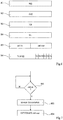
- the figure 7 is a flowchart illustrating an embodiment of a data transfer method by direct access in memory. More specifically, the figure 7 illustrates in more detail step 202 of the method of figure 2 .
- step 801 (ctrl-in?) Implemented by the circuit 14, all the parameters of the data transfer to be executed are stored in the registers of the register bank.
- Step 801 consists in detecting the ctrl-in condition for start of transfer, stored in register R5 in this example.
- Step 801 is repeated (output N of block 801) as long as this ctrl-in condition is not detected.
- step 802 MAKE TRANSFER
- step 804 GENERAL ctrl-out
- the second transfer can only start after the generation of the ctrl-out event of the first transfer.
- the first and second transfers therefore the first and second applications, can be synchronized with each other, directly at the level of the circuit 14, without intervention by the central unit 11 and while these applications are in being executed.
- the forecast of a ctrl-in condition and a ctrl-out event for at least certain data transfers from several applications executed by the system 1 makes it possible to synchronize these applications with one another, without resorting to the central processing unit which can be put on standby or even off during the execution of these applications.
- an additional parameter is provided indicating when the condition ctrl-in must be detected during a transfer of several data, for example before the transfer of the first data or before the transfer of each data.
- an additional parameter is provided indicating when the ctrl-out event must be generated during the transfer of several data, for example after the transfer of the last data or after the transfer of each data.
- the registers and records in the list are then adapted to integrate these additional parameters.
- the process of figure 7 is also adapted accordingly.
- steps 801, 802 and 804 are implemented for each datum transferred, step 802 then corresponding to the transfer of the datum.
- Predicting one or more additional parameters to indicate the moment (s) of a transfer when a ctrl-in condition must be detected and the moment (s) when a ctrl-out event must be generated makes it possible to control the granularity at which s 'synchronizes between applications executed in parallel by system 1.
- the ctrl-in condition of a transfer on a channel can correspond to the detection of an event other than a ctrl-out event generated during a transfer on another channel, for example to an interruption generated in the system 1.
- each ctrl-in condition can correspond to the detection of a level change, for example the passage from a high level to a low level or vice versa, of a signal corresponding to this condition.
- Each ctrl-out event consists, for example, in changing the level of a signal corresponding to this event.
- each record in the linked list contains as many fields as there are registers.
- the registers and records described in relation to the figures 3 to 7 can integrate one or more additional parameters so as to manage transfers by data blocks and / or, in a range of source and / or destination addresses, address shifts between two data or two data blocks to be transferred successive.
- the registers and the records are adapted so as to manage transfers by blocks of data
- the condition ctrl-in is detected before the transfer of each block and / or that the ctrl-out event is generated after the transfer of each block.
- the parameter (s) indicating when to detect the ctrl-in condition and / or generate the ctrl-out event will then be adapted accordingly, as will the method described in relation to the figure 7 .
- a parameter can indicate whether the data and / or the transfer data blocks corresponding to a record must be transferred piecemeal or by burst ("burst").
Landscapes
- Engineering & Computer Science (AREA)
- Theoretical Computer Science (AREA)
- Physics & Mathematics (AREA)
- General Engineering & Computer Science (AREA)
- General Physics & Mathematics (AREA)
- Human Computer Interaction (AREA)
- Information Retrieval, Db Structures And Fs Structures Therefor (AREA)
Applications Claiming Priority (1)
| Application Number | Priority Date | Filing Date | Title |
|---|---|---|---|
| FR1856705A FR3084179A1 (fr) | 2018-07-19 | 2018-07-19 | Acces direct en memoire |
Publications (1)
| Publication Number | Publication Date |
|---|---|
| EP3598314A1 true EP3598314A1 (de) | 2020-01-22 |
Family
ID=65031473
Family Applications (1)
| Application Number | Title | Priority Date | Filing Date |
|---|---|---|---|
| EP19186866.0A Withdrawn EP3598314A1 (de) | 2018-07-19 | 2019-07-17 | Direkter speicherzugang |
Country Status (4)
| Country | Link |
|---|---|
| US (1) | US10997087B2 (de) |
| EP (1) | EP3598314A1 (de) |
| CN (2) | CN110737617B (de) |
| FR (2) | FR3084179A1 (de) |
Families Citing this family (1)
| Publication number | Priority date | Publication date | Assignee | Title |
|---|---|---|---|---|
| EP3598315B1 (de) | 2018-07-19 | 2022-12-28 | STMicroelectronics (Grenoble 2) SAS | Direkter speicherzugang |
Citations (2)
| Publication number | Priority date | Publication date | Assignee | Title |
|---|---|---|---|---|
| WO2001029656A2 (en) * | 1999-10-20 | 2001-04-26 | Infineon Technologies North America Corp. | Linked list dma descriptor architecture |
| US20060050693A1 (en) * | 2004-09-03 | 2006-03-09 | James Bury | Building data packets for an advanced switching fabric |
Family Cites Families (11)
| Publication number | Priority date | Publication date | Assignee | Title |
|---|---|---|---|---|
| JP3268591B2 (ja) * | 1995-11-22 | 2002-03-25 | 株式会社日立製作所 | グラフィックスプロセッサでの並列処理方法 |
| US6782365B1 (en) * | 1996-12-20 | 2004-08-24 | Qwest Communications International Inc. | Graphic interface system and product for editing encoded audio data |
| US6145027A (en) * | 1997-07-09 | 2000-11-07 | Texas Instruments Incorporated | DMA controller with split channel transfer capability and FIFO buffering allowing transmit channel to get ahead of corresponding receive channel by preselected number of elements |
| US20060259657A1 (en) * | 2005-05-10 | 2006-11-16 | Telairity Semiconductor, Inc. | Direct memory access (DMA) method and apparatus and DMA for video processing |
| US7904614B1 (en) * | 2006-06-27 | 2011-03-08 | Marvell International Ltd. | Direct memory access controller with multiple transaction functionality |
| US7721018B2 (en) * | 2006-08-24 | 2010-05-18 | Microchip Technology Incorporated | Direct memory access controller with flow control |
| JP5423483B2 (ja) * | 2010-03-04 | 2014-02-19 | 株式会社リコー | データ転送制御装置 |
| US9569384B2 (en) * | 2013-03-14 | 2017-02-14 | Infineon Technologies Ag | Conditional links for direct memory access controllers |
| US20150186068A1 (en) * | 2013-12-27 | 2015-07-02 | Sandisk Technologies Inc. | Command queuing using linked list queues |
| CN106375249B (zh) * | 2016-09-22 | 2019-10-01 | 盛科网络(苏州)有限公司 | 交换芯片的控制方法及控制系统 |
| US10191871B2 (en) * | 2017-06-20 | 2019-01-29 | Infineon Technologies Ag | Safe double buffering using DMA safe linked lists |
-
2018
- 2018-07-19 FR FR1856705A patent/FR3084179A1/fr not_active Ceased
- 2018-11-02 FR FR1871349A patent/FR3084178A1/fr not_active Ceased
-
2019
- 2019-07-15 US US16/511,362 patent/US10997087B2/en active Active
- 2019-07-16 CN CN201910641180.4A patent/CN110737617B/zh active Active
- 2019-07-17 EP EP19186866.0A patent/EP3598314A1/de not_active Withdrawn
- 2019-07-19 CN CN201910654666.1A patent/CN110990308B/zh active Active
Patent Citations (2)
| Publication number | Priority date | Publication date | Assignee | Title |
|---|---|---|---|---|
| WO2001029656A2 (en) * | 1999-10-20 | 2001-04-26 | Infineon Technologies North America Corp. | Linked list dma descriptor architecture |
| US20060050693A1 (en) * | 2004-09-03 | 2006-03-09 | James Bury | Building data packets for an advanced switching fabric |
Also Published As
| Publication number | Publication date |
|---|---|
| FR3084178A1 (fr) | 2020-01-24 |
| US10997087B2 (en) | 2021-05-04 |
| US20200026662A1 (en) | 2020-01-23 |
| CN110737617B (zh) | 2024-10-25 |
| CN110990308A (zh) | 2020-04-10 |
| CN110737617A (zh) | 2020-01-31 |
| FR3084179A1 (fr) | 2020-01-24 |
| CN110990308B (zh) | 2025-03-18 |
Similar Documents
| Publication | Publication Date | Title |
|---|---|---|
| BE1001068A4 (fr) | Methode d'ouverture rapide de fichiers a disques identifies par la denomination de chemins. | |
| FR2844613A1 (fr) | Systeme pour le transfert rapide des donnees | |
| FR2697663A1 (fr) | Circuit de test de mémoire. | |
| WO2016132052A1 (fr) | Circuit dram muni d'un processeur integre | |
| EP3598314A1 (de) | Direkter speicherzugang | |
| EP3598315B1 (de) | Direkter speicherzugang | |
| EP2530586B1 (de) | Verfahren zur Erzeugung einer Software | |
| FR2759178A1 (fr) | Circuit de gestion de memoire dans un environnement multi-utilisateurs avec requete et priorite d'acces | |
| WO2017148856A1 (fr) | Procede de d'affichage d'une animation lors de la phase de demarrage d'un dispositif electronique et dispositif electronique associe | |
| EP3716086B1 (de) | Direkter speicherzugang | |
| EP1233419A2 (de) | Auffrischungsverfahren eines dynamischen Speichers | |
| EP4055485B1 (de) | Verfahren zum ausführen einer transaktion | |
| FR2865291A1 (fr) | Procede de transfert de donnees dans un systeme multiprocesseur, systeme multiprocesseur et processeur mettant en oeuvre ce procede | |
| FR3142592A1 (fr) | Mémoire non volatile | |
| FR2801388A1 (fr) | Procede de commande de memoire dram rapide et controleur adapte | |
| EP1594065A1 (de) | System auf einem Chip mit einem Arbiter und Speicherschlüssel mit solchem System | |
| FR3033420A1 (fr) | Procede de gestion de donnees relatives a une mission d'aeronefs et module de gestion de donnees correspondant | |
| WO2021073990A1 (fr) | Procede d'aide a l'identification de secteurs vierges d'une memoire non-volatile d'un microcontroleur | |
| EP3215933A1 (de) | Verfahren für rekonfigurierbare grobkornarchitektur und vorrichtung zur ausführung eines anwendungscodes in seiner ganzheit | |
| EP3792771A1 (de) | Programmtest | |
| CN118012400A (zh) | 针对程序的方法集合获取方法和装置 | |
| FR2897174A1 (fr) | Processeur comportant une interface de debogage integree controlee par l'unite de traitement du processeur | |
| EP0928002B1 (de) | Zweifachspeicher für digitalen Signalprozessor | |
| FR2922037A1 (fr) | Procede de securisation de donnees en memoire vive | |
| WO2004046930A1 (fr) | Dispositif a liaison serie de surveillance d'un microprocesseur |
Legal Events
| Date | Code | Title | Description |
|---|---|---|---|
| PUAI | Public reference made under article 153(3) epc to a published international application that has entered the european phase |
Free format text: ORIGINAL CODE: 0009012 |
|
| STAA | Information on the status of an ep patent application or granted ep patent |
Free format text: STATUS: REQUEST FOR EXAMINATION WAS MADE |
|
| 17P | Request for examination filed |
Effective date: 20190717 |
|
| AK | Designated contracting states |
Kind code of ref document: A1 Designated state(s): AL AT BE BG CH CY CZ DE DK EE ES FI FR GB GR HR HU IE IS IT LI LT LU LV MC MK MT NL NO PL PT RO RS SE SI SK SM TR |
|
| AX | Request for extension of the european patent |
Extension state: BA ME |
|
| STAA | Information on the status of an ep patent application or granted ep patent |
Free format text: STATUS: EXAMINATION IS IN PROGRESS |
|
| 17Q | First examination report despatched |
Effective date: 20201222 |
|
| STAA | Information on the status of an ep patent application or granted ep patent |
Free format text: STATUS: THE APPLICATION IS DEEMED TO BE WITHDRAWN |
|
| 18D | Application deemed to be withdrawn |
Effective date: 20210504 |