EP3598628A1 - Dispositif de semi-conducteur, module de commutation pourvu de dispositif de semi-conducteur et convertisseurs modulaires à plusieurs étages pourvu de module de commutation - Google Patents
Dispositif de semi-conducteur, module de commutation pourvu de dispositif de semi-conducteur et convertisseurs modulaires à plusieurs étages pourvu de module de commutation Download PDFInfo
- Publication number
- EP3598628A1 EP3598628A1 EP19184037.0A EP19184037A EP3598628A1 EP 3598628 A1 EP3598628 A1 EP 3598628A1 EP 19184037 A EP19184037 A EP 19184037A EP 3598628 A1 EP3598628 A1 EP 3598628A1
- Authority
- EP
- European Patent Office
- Prior art keywords
- semiconductor
- diode
- voltage
- energy store
- semiconductor arrangement
- Prior art date
- Legal status (The legal status is an assumption and is not a legal conclusion. Google has not performed a legal analysis and makes no representation as to the accuracy of the status listed.)
- Granted
Links
Images


Classifications
-
- H—ELECTRICITY
- H02—GENERATION; CONVERSION OR DISTRIBUTION OF ELECTRIC POWER
- H02M—APPARATUS FOR CONVERSION BETWEEN AC AND AC, BETWEEN AC AND DC, OR BETWEEN DC AND DC, AND FOR USE WITH MAINS OR SIMILAR POWER SUPPLY SYSTEMS; CONVERSION OF DC OR AC INPUT POWER INTO SURGE OUTPUT POWER; CONTROL OR REGULATION THEREOF
- H02M7/00—Conversion of AC power input into DC power output; Conversion of DC power input into AC power output
- H02M7/42—Conversion of DC power input into AC power output without possibility of reversal
- H02M7/44—Conversion of DC power input into AC power output without possibility of reversal by static converters
- H02M7/48—Conversion of DC power input into AC power output without possibility of reversal by static converters using discharge tubes with control electrode or semiconductor devices with control electrode
- H02M7/483—Converters with outputs that each can have more than two voltages levels
-
- H—ELECTRICITY
- H02—GENERATION; CONVERSION OR DISTRIBUTION OF ELECTRIC POWER
- H02M—APPARATUS FOR CONVERSION BETWEEN AC AND AC, BETWEEN AC AND DC, OR BETWEEN DC AND DC, AND FOR USE WITH MAINS OR SIMILAR POWER SUPPLY SYSTEMS; CONVERSION OF DC OR AC INPUT POWER INTO SURGE OUTPUT POWER; CONTROL OR REGULATION THEREOF
- H02M7/00—Conversion of AC power input into DC power output; Conversion of DC power input into AC power output
- H02M7/42—Conversion of DC power input into AC power output without possibility of reversal
- H02M7/44—Conversion of DC power input into AC power output without possibility of reversal by static converters
- H02M7/48—Conversion of DC power input into AC power output without possibility of reversal by static converters using discharge tubes with control electrode or semiconductor devices with control electrode
- H02M7/483—Converters with outputs that each can have more than two voltages levels
- H02M7/4835—Converters with outputs that each can have more than two voltages levels comprising two or more cells, each including a switchable capacitor, the capacitors having a nominal charge voltage which corresponds to a given fraction of the input voltage, and the capacitors being selectively connected in series to determine the instantaneous output voltage
-
- H—ELECTRICITY
- H02—GENERATION; CONVERSION OR DISTRIBUTION OF ELECTRIC POWER
- H02M—APPARATUS FOR CONVERSION BETWEEN AC AND AC, BETWEEN AC AND DC, OR BETWEEN DC AND DC, AND FOR USE WITH MAINS OR SIMILAR POWER SUPPLY SYSTEMS; CONVERSION OF DC OR AC INPUT POWER INTO SURGE OUTPUT POWER; CONTROL OR REGULATION THEREOF
- H02M7/00—Conversion of AC power input into DC power output; Conversion of DC power input into AC power output
- H02M7/42—Conversion of DC power input into AC power output without possibility of reversal
- H02M7/44—Conversion of DC power input into AC power output without possibility of reversal by static converters
- H02M7/48—Conversion of DC power input into AC power output without possibility of reversal by static converters using discharge tubes with control electrode or semiconductor devices with control electrode
- H02M7/483—Converters with outputs that each can have more than two voltages levels
- H02M7/49—Combination of the output voltage waveforms of a plurality of converters
-
- H—ELECTRICITY
- H10—SEMICONDUCTOR DEVICES; ELECTRIC SOLID-STATE DEVICES NOT OTHERWISE PROVIDED FOR
- H10W—GENERIC PACKAGES, INTERCONNECTIONS, CONNECTORS OR OTHER CONSTRUCTIONAL DETAILS OF DEVICES COVERED BY CLASS H10
- H10W40/00—Arrangements for thermal protection or thermal control
- H10W40/40—Arrangements for thermal protection or thermal control involving heat exchange by flowing fluids
- H10W40/47—Arrangements for thermal protection or thermal control involving heat exchange by flowing fluids by flowing liquids, e.g. forced water cooling
-
- H—ELECTRICITY
- H10—SEMICONDUCTOR DEVICES; ELECTRIC SOLID-STATE DEVICES NOT OTHERWISE PROVIDED FOR
- H10W—GENERIC PACKAGES, INTERCONNECTIONS, CONNECTORS OR OTHER CONSTRUCTIONAL DETAILS OF DEVICES COVERED BY CLASS H10
- H10W42/00—Arrangements for protection of devices
- H10W42/80—Arrangements for protection of devices protecting against overcurrent or overload, e.g. fuses or shunts
-
- H—ELECTRICITY
- H10—SEMICONDUCTOR DEVICES; ELECTRIC SOLID-STATE DEVICES NOT OTHERWISE PROVIDED FOR
- H10W—GENERIC PACKAGES, INTERCONNECTIONS, CONNECTORS OR OTHER CONSTRUCTIONAL DETAILS OF DEVICES COVERED BY CLASS H10
- H10W90/00—Package configurations
-
- H—ELECTRICITY
- H02—GENERATION; CONVERSION OR DISTRIBUTION OF ELECTRIC POWER
- H02M—APPARATUS FOR CONVERSION BETWEEN AC AND AC, BETWEEN AC AND DC, OR BETWEEN DC AND DC, AND FOR USE WITH MAINS OR SIMILAR POWER SUPPLY SYSTEMS; CONVERSION OF DC OR AC INPUT POWER INTO SURGE OUTPUT POWER; CONTROL OR REGULATION THEREOF
- H02M1/00—Details of apparatus for conversion
- H02M1/32—Means for protecting converters other than automatic disconnection
- H02M1/325—Means for protecting converters other than automatic disconnection with means for allowing continuous operation despite a fault, i.e. fault tolerant converters
Definitions
- the invention relates to a semiconductor arrangement with at least two semiconductor switches that can be switched off, an energy store, two external connections, the energy store being connected to the semiconductor switches in such a way that a voltage can be generated at the connections that corresponds to an energy storage voltage present at the energy store or a zero voltage, a protective semiconductor in a parallel connection to the energy store, a diode series connection in a further parallel connection to the energy store, the diode series connection comprising at least two diodes arranged in series, a first diode of the diode series connection being connected to the first semiconductor switch and a second diode of the diode series connection being connected antiparallel to the second semiconductor switch, with which one Forward direction of the first diode against a forward direction of the first semiconductor switch and a forward direction of the second diode against a forward direction direction of the second semiconductor switch are directed.
- the modular multi-stage converter 1 shown comprises in its basic structure two converter arms 2a, 2b per converter phase 3a-c. Each converter arm comprises a series connection of numerous switch modules 4. Frequently used switch module types are switch modules in half-bridge or full-bridge connection. If a switching module fails, it must be bridged to ensure that the multi-stage converter continues to operate until the next maintenance process. Mechanical bypass switches are usually used to bypass the switching modules.
- a short circuit on the DC voltage side can be a particularly critical fault in certain configurations.
- the AC voltage impressed on the AC side generates a high short-circuit current into the DC fault. This flows uncontrolled through the diode series connection. The components of the circuit must survive this high fault current without damage until it has been clarified / switched off externally (generally by circuit breakers installed on the AC side).
- diode chips are usually used, which are connected to the other components by means of bonding wires. The diodes have only a low thermal capacity, which is not sufficient in the event of a fault to avoid possible destruction of the semiconductor arrangement.
- the particularly loaded diode is relieved by an additional protective component arranged in parallel.
- An appropriate semiconductor arrangement is for example from the DE 103 23 220 B4 known.
- the known semiconductor arrangement forms a full-bridge circuit for forming a switching module of a modular matrix converter.
- the protective semiconductor is activated as a function of a short-circuit current of the energy store in such a way that it is permanently alloyed, a short-circuit path being provided in parallel with the energy store.
- the present invention is based on the object of proposing a semiconductor arrangement of the type mentioned at the outset which is as inexpensive and reliable as possible.
- the diodes of the diode series circuit are disk cell diodes which are mechanically clamped in at least one diode clamping assembly.
- the disc cell diodes can be mechanically clamped together in a common diode clamping assembly.
- the disk cell diodes can be mechanically clamped individually in a diode clamping assembly.
- Disc cell diodes have a higher thermal capacity due to their relatively large area. This advantageously reduces the risk of the semiconductor arrangement being destroyed in the event of a fault.
- the disc cell diodes have an increased current carrying capacity, so that they can carry the short-circuit current in the event of a fault.
- the provision of the aforementioned protective component parallel to one of the diodes can thus advantageously be dispensed with, which enables a cost advantage.
- the semiconductor arrangement can be bridged in the event of a fault.
- an additional bypass switch can advantageously be dispensed with, which results in a further cost advantage.
- the diode clamping assembly is preferably arranged spatially between the protective semiconductor and the semiconductor switches. In this way, the disk cell diodes are arranged close to the intermediate circuit of the energy store. As a result, the maximum power loss at the disk cell diode can advantageously be reduced.
- the protective semiconductor is preferably a thyristor.
- Thyristors are controllable semiconductors.
- a short-circuit path can be provided in parallel to the energy store by specifically controlling the thyristor in the event of a fault.
- the thyristor can be ignited in the event of a fault, the thyristor preferably being destroyed by the energy stored in the energy store.
- the ignition of the Thyristors can take place after falling below a predetermined amount of energy in the energy store or when a predetermined current rise threshold is exceeded. If there is not enough energy in the energy store, it can be charged via the disk cell diodes during regular operation of the semiconductor arrangement.
- An explosion of the semiconductor arrangement can advantageously be prevented by igniting the protective semiconductor. This can save an explosion-proof housing for the semiconductor arrangement.
- the thyristor can, for example, be arranged in a thyristor junction.
- the electrical contacting takes place via the thyristor tension assembly. This configuration provides a particularly reliable low-resistance short-circuit path after the thyristor has been alloyed.
- the disk cell diodes are preferably cooled on both sides. Cooling elements can be present in the diode clamping structure, for example, adjacent to each disk cell diode.
- the cooling elements can be cooling plates, for example, through which a cooling medium flows. Due to the cooling of the disk cell diodes on both sides, a particularly high output can advantageously be conducted through the disk cell diodes.
- the semiconductor arrangement suitably has a first DC voltage pole which is connected to a first connection of the energy store and a second DC voltage pole which is connected to a second connection of the energy store, the DC voltage poles being at least partially formed by external cooling plates for cooling the semiconductor arrangement.
- the intermediate circuit of the semiconductor arrangement is defined by the DC voltage poles.
- the cooling plates are therefore used as electrical connections in the intermediate circuit used, which allows a particularly compact structure of the semiconductor device.
- the diode series connection is preferably clamped between the outer cooling plates.
- the cooling plates can advantageously be used to cool the disk cell diodes.
- a first of the semiconductor switches is arranged between the first DC voltage pole and an external AC voltage connection of the semiconductor arrangement and a second of the semiconductor switches is arranged between the external AC voltage connection of the semiconductor arrangement and the second DC voltage pole.
- the external AC voltage connection is used to connect the semiconductor arrangement, for example to a further semiconductor arrangement, to form a series connection.
- the semiconductor arrangement suitably has a further external AC voltage connection, the arrangement of which depends on the configuration of the semiconductor arrangement.
- the further AC voltage connection can be connected directly to one of the DC voltage poles.
- the semiconductor switches are accordingly arranged opposite one another and can be connected to the DC voltage poles, for example, by means of the outer cooling plates. This embodiment allows a particularly compact and robust construction of the semiconductor arrangement.
- the semiconductor arrangement can, for example, form a half-bridge circuit or a full-bridge circuit.
- These circuits are known to those skilled in the art as being particularly effective and are particularly suitable for use in a modular multi-stage converter.
- a switching module in half-bridge circuit 10 is shown in Figure 2 shown.
- the half-bridge circuit 10 has two semiconductor switches 11, 12 that can be switched off (in the illustrated case, they are IGBT switches, wherein in general other switchable semiconductor switches, such as IGCT or the like, are also used ) and the energy storage device 13, the semiconductor switches 11, 12 being connected to the energy storage device 13 in such a way that an energy storage voltage Vc or Zero voltage can be generated.
- a switching module in full bridge circuit 30 is in Figure 3 shown.
- the full bridge circuit 30 has a first semiconductor switch 31 and a second semiconductor switch 22, both in the form of IGBTs.
- the forward direction of the two semiconductor switches 31 and 32 is rectified.
- the full-bridge module circuit 30 further comprises a third semiconductor switch 33 and a fourth semiconductor switch 34, both likewise in the form of IGBTs.
- the IGBTs can be replaced by other semiconductor switches that can be switched off.
- the forward direction of the two semiconductor switches 33 and 34 is rectified.
- a switching module capacitor 35 is arranged in parallel with the two series connections of the semiconductor switches.
- the first connection X1 is arranged at a potential point 36 between the semiconductor switches 31, 32
- the second connection X2 is arranged at a potential point 37 between the semiconductor switches 33, 34.
- a free-wheeling diode D is connected antiparallel to each of the semiconductor switches 31-34.
- the voltage drop across the terminals X1, X2 can be generated, which corresponds to the voltage drop Vc across the switch module capacitor 35, but the voltage drop across the switch module capacitor 35 with opposite polarity (-Vc) or the zero voltage.
- switching modules are, for example, the so-called double-clamp submodule, which is described in the article " Modular Multilevel Converter: A Universal Concept for HVDC Networks and Extended DC Bus Applications "by R. Marquardt the so-called five-level cross connected submodule, known from the article " Five Level Cross Connected Cell for Cascaded Converters "by A. Nami et al. and the double submodule Circuit, which in the post " A Submodule Implementation for Parallel Connection of Capacitors in Modular Multilevel Converters "by K. Ilves et al. is disclosed.
- the invention further relates to a switching module for a modular multi-stage converter.
- the object of the invention is to provide a type-specific switching module which enables the multi-stage converter to operate as reliably as possible and at the same time is as inexpensive as possible.
- a type-appropriate switching module which comprises a semiconductor arrangement according to the invention.
- the switching module expediently comprises further components, such as a control circuit and / or communication device, which are designed and set up for operating the switching module in a modular multistage converter.
- the invention relates to a modular multi-stage converter.
- Modular multi-stage converters are, as already stated, known from the prior art.
- Each of the switching modules of the modular multi-stage converter can be controlled individually by means of a control device.
- a voltage drop across one of the converter arms is equal to the sum of voltages drop across the associated switching modules.
- a particularly advantageous step-shaped converter voltage of the MMC can be generated at its AC voltage connection.
- the object of the invention is to propose a modular multi-stage converter which is as inexpensive and reliable as possible.
- the object is achieved in that the modular multi-stage converter comprises a series connection of the switching modules according to the invention.
- the invention relates to a high-voltage direct current transmission system with a modular multi-stage converter.
- Such high-voltage direct current transmission systems are from the prior art, for example from WO 2016/155 850 A1 known. They are usually used for coupling AC voltage networks, the electrical losses during power transmission between the AC voltage networks being advantageously low.
- the object of the invention is to provide a high-voltage direct current transmission system of the type which is as reliable as possible in operation and inexpensive to manufacture.
- the modular multi-stage converter of the high-voltage direct current transmission system according to the invention is a modular multi-stage converter according to the invention.
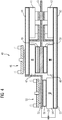
- Figure 4 shows an embodiment of a semiconductor device according to the invention in a schematic side view.
- the semiconductor arrangement 40 comprises a first switchable semiconductor switch 41 in the form of an IGBT and a second switchable semiconductor switch 42 also in the form of an IGBT.
- the two semiconductor switches 41, 42 are arranged as chips on a substrate and face one another on the chip side.
- An AC voltage connection 43 of the semiconductor arrangement 40 is arranged between the semiconductor switches 41, 42.
- An outer cooling plate 44 and 45 is provided in each case for cooling the two semiconductor switches 41, 42.
- the AC voltage connection 43 and the outer cooling plate 44 form the two outer connections of the semiconductor arrangement 40.
- a diode clamping assembly 46 is mechanically clamped between the two cooling plates 44, 45.
- the diode clamping assembly 46 comprises disc cell diodes 47 and 48 which are electrically contacted to one another in a diode series connection and serve as free-wheeling diodes for the semiconductor switches 41, 42.
- the disk cell diodes 47, 48 are each cooled on both sides by means of the cooling plates 44, 45 and cooling disks 49, 50.
- the semiconductor arrangement 40 further comprises an energy store 51 in the form of an intermediate circuit capacitor, the connections of which form two DC voltage poles 52 and 53 of the semiconductor arrangement.
- a protective semiconductor in the form of a protective thyristor 54 is arranged in a thyristor clamping assembly 55 parallel to the energy store 51.
- the protective thyristor 54 is by means of the outer one Cooling plate 45 and another cooling plate 56 cooled on both sides.
Landscapes
- Engineering & Computer Science (AREA)
- Power Engineering (AREA)
- Rectifiers (AREA)
- Inverter Devices (AREA)
Applications Claiming Priority (1)
| Application Number | Priority Date | Filing Date | Title |
|---|---|---|---|
| DE102018211900.7A DE102018211900A1 (de) | 2018-07-17 | 2018-07-17 | Halbleiteranordnung, Schaltmodul mit der Halbleiteranordnung und modularer Mehrstufenumrichter mit dem Schaltmodul |
Publications (2)
| Publication Number | Publication Date |
|---|---|
| EP3598628A1 true EP3598628A1 (fr) | 2020-01-22 |
| EP3598628B1 EP3598628B1 (fr) | 2022-06-22 |
Family
ID=67145659
Family Applications (1)
| Application Number | Title | Priority Date | Filing Date |
|---|---|---|---|
| EP19184037.0A Active EP3598628B1 (fr) | 2018-07-17 | 2019-07-03 | Dispositif de semi-conducteur, module de commutation pourvu de dispositif de semi-conducteur et convertisseur modulaire à plusieurs étages pourvu de module de commutation |
Country Status (2)
| Country | Link |
|---|---|
| EP (1) | EP3598628B1 (fr) |
| DE (1) | DE102018211900A1 (fr) |
Cited By (1)
| Publication number | Priority date | Publication date | Assignee | Title |
|---|---|---|---|---|
| CN113193774A (zh) * | 2021-05-10 | 2021-07-30 | 昆明理工大学 | 一种mmc五电平半桥反串联子模块flhasm拓扑结构 |
Citations (6)
| Publication number | Priority date | Publication date | Assignee | Title |
|---|---|---|---|---|
| DE10245288A1 (de) * | 2002-09-27 | 2004-04-08 | Siemens Ag | Leistungsteil für einen Stromumrichter und Verfahren zur Herstellung desselben |
| JP2004158485A (ja) * | 2002-11-01 | 2004-06-03 | Honda Motor Co Ltd | 圧接型半導体装置 |
| DE10323220B4 (de) | 2003-05-22 | 2014-07-17 | Siemens Aktiengesellschaft | Kurzschluss-Schaltung für einen Teilumrichter |
| JP2015002564A (ja) * | 2013-06-13 | 2015-01-05 | 株式会社日立製作所 | 電力変換装置 |
| WO2016155850A1 (fr) | 2015-04-02 | 2016-10-06 | Siemens Aktiengesellschaft | Ensemble convertisseur et procédé de protection contre les court-circuits dudit ensemble convertisseur |
| WO2018006970A1 (fr) * | 2016-07-07 | 2018-01-11 | Abb Schweiz Ag | Pile d'énergie à semi-conducteur d'un convertisseur modulaire multiniveaux |
Family Cites Families (2)
| Publication number | Priority date | Publication date | Assignee | Title |
|---|---|---|---|---|
| WO2013044961A1 (fr) * | 2011-09-29 | 2013-04-04 | Siemens Aktiengesellschaft | Dispositif de protection contre les courants de court-circuit destiné à un sous-module d'un convertisseur modulaire à étages multiples (mmc) |
| KR102269017B1 (ko) * | 2016-09-05 | 2021-06-25 | 지멘스 악티엔게젤샤프트 | 전기 에너지 저장 유닛을 방전시키기 위한 방법 |
-
2018
- 2018-07-17 DE DE102018211900.7A patent/DE102018211900A1/de not_active Withdrawn
-
2019
- 2019-07-03 EP EP19184037.0A patent/EP3598628B1/fr active Active
Patent Citations (6)
| Publication number | Priority date | Publication date | Assignee | Title |
|---|---|---|---|---|
| DE10245288A1 (de) * | 2002-09-27 | 2004-04-08 | Siemens Ag | Leistungsteil für einen Stromumrichter und Verfahren zur Herstellung desselben |
| JP2004158485A (ja) * | 2002-11-01 | 2004-06-03 | Honda Motor Co Ltd | 圧接型半導体装置 |
| DE10323220B4 (de) | 2003-05-22 | 2014-07-17 | Siemens Aktiengesellschaft | Kurzschluss-Schaltung für einen Teilumrichter |
| JP2015002564A (ja) * | 2013-06-13 | 2015-01-05 | 株式会社日立製作所 | 電力変換装置 |
| WO2016155850A1 (fr) | 2015-04-02 | 2016-10-06 | Siemens Aktiengesellschaft | Ensemble convertisseur et procédé de protection contre les court-circuits dudit ensemble convertisseur |
| WO2018006970A1 (fr) * | 2016-07-07 | 2018-01-11 | Abb Schweiz Ag | Pile d'énergie à semi-conducteur d'un convertisseur modulaire multiniveaux |
Cited By (2)
| Publication number | Priority date | Publication date | Assignee | Title |
|---|---|---|---|---|
| CN113193774A (zh) * | 2021-05-10 | 2021-07-30 | 昆明理工大学 | 一种mmc五电平半桥反串联子模块flhasm拓扑结构 |
| CN113193774B (zh) * | 2021-05-10 | 2023-10-31 | 昆明理工大学 | 一种mmc五电平半桥反串联子模块flhasm拓扑结构 |
Also Published As
| Publication number | Publication date |
|---|---|
| EP3598628B1 (fr) | 2022-06-22 |
| DE102018211900A1 (de) | 2020-01-23 |
Similar Documents
| Publication | Publication Date | Title |
|---|---|---|
| DE10323220B4 (de) | Kurzschluss-Schaltung für einen Teilumrichter | |
| EP2425513B1 (fr) | Module avec un dispositif de stockage d'énergie électrique supplémentaire pour un convertisseur multi-niveaux modulaire | |
| EP2678931B1 (fr) | Convertisseur modulaire à étapes multiples, ayant des commutateurs semi-conducteurs de puissance conducteurs en sens inverse | |
| EP3072143B1 (fr) | Dispositif de commutation d'un courant continu | |
| DE102007018344A1 (de) | Vorrichtung zum Schutz von Umrichtermodulen | |
| DE102015109466A1 (de) | Stromrichter-Submodul mit Kurzschlusseinrichtung und Stromrichter mit diesem | |
| WO2016188589A1 (fr) | Module convertisseur commandé par tension | |
| EP2338214A1 (fr) | Dispositif présentant un convertisseur de fréquence | |
| EP2810291B1 (fr) | Appareil pour commuter de courants continus | |
| EP3556000A1 (fr) | Module pour convertisseurs multipoints modulaires avec court-circuiteur et limite de courant de condensateur | |
| EP3783783B1 (fr) | Agencement de régulation d'un flux de puissance dans un réseau à tension alternative et procédé de protection de l'agencement | |
| EP3622621B1 (fr) | Onduleur à plusieurs niveaux | |
| EP3487026A1 (fr) | Dispositif onduleur destiné à la stabilisation d'un réseau de courant alternatif | |
| EP3662572A1 (fr) | Sous-module conçu pour un convertisseur modulaire multiniveaux | |
| EP3598628B1 (fr) | Dispositif de semi-conducteur, module de commutation pourvu de dispositif de semi-conducteur et convertisseur modulaire à plusieurs étages pourvu de module de commutation | |
| EP3639360B1 (fr) | Ensemble convertisseur à parafoudre à module de phase ainsi que procédé pour protéger ledit ensemble convertisseur contre des court-circuits | |
| DE102016202661A1 (de) | Vorrichtung zum Schalten eines Gleichstroms in einem Pol eines Gleichspannungsnetzes | |
| EP2904625A1 (fr) | Disjoncteur à haute tension continue | |
| DE102013213986B4 (de) | Dreipunkt-Stromrichter | |
| DE102017202208A1 (de) | Versorgungseinrichtung für ein elektrisches Modul mit Sicherungselement | |
| DE202020101757U1 (de) | Sicherungsanordnung in MMC-Zelle | |
| EP3818549B1 (fr) | Agencement présentant un module d'un convertisseur de puissance multiniveau | |
| EP3753048B1 (fr) | Circuit, module convertisseur et procédé de fonctionnement du module convertisseur | |
| DD278453A1 (de) | Schaltungsanordnung zur erzeugung der zwischenkreisspannung fuer transistorstellglieder | |
| EP0450126B1 (fr) | Dispositif pour protéger et surveiller une résistance à impulsion pour un circuit intermédiaire de convertisseur de tension |
Legal Events
| Date | Code | Title | Description |
|---|---|---|---|
| PUAI | Public reference made under article 153(3) epc to a published international application that has entered the european phase |
Free format text: ORIGINAL CODE: 0009012 |
|
| STAA | Information on the status of an ep patent application or granted ep patent |
Free format text: STATUS: THE APPLICATION HAS BEEN PUBLISHED |
|
| AK | Designated contracting states |
Kind code of ref document: A1 Designated state(s): AL AT BE BG CH CY CZ DE DK EE ES FI FR GB GR HR HU IE IS IT LI LT LU LV MC MK MT NL NO PL PT RO RS SE SI SK SM TR |
|
| AX | Request for extension of the european patent |
Extension state: BA ME |
|
| STAA | Information on the status of an ep patent application or granted ep patent |
Free format text: STATUS: REQUEST FOR EXAMINATION WAS MADE |
|
| 17P | Request for examination filed |
Effective date: 20200406 |
|
| RBV | Designated contracting states (corrected) |
Designated state(s): AL AT BE BG CH CY CZ DE DK EE ES FI FR GB GR HR HU IE IS IT LI LT LU LV MC MK MT NL NO PL PT RO RS SE SI SK SM TR |
|
| STAA | Information on the status of an ep patent application or granted ep patent |
Free format text: STATUS: EXAMINATION IS IN PROGRESS |
|
| 17Q | First examination report despatched |
Effective date: 20200701 |
|
| RAP1 | Party data changed (applicant data changed or rights of an application transferred) |
Owner name: SIEMENS ENERGY GLOBAL GMBH & CO. KG |
|
| GRAP | Despatch of communication of intention to grant a patent |
Free format text: ORIGINAL CODE: EPIDOSNIGR1 |
|
| STAA | Information on the status of an ep patent application or granted ep patent |
Free format text: STATUS: GRANT OF PATENT IS INTENDED |
|
| INTG | Intention to grant announced |
Effective date: 20220201 |
|
| GRAS | Grant fee paid |
Free format text: ORIGINAL CODE: EPIDOSNIGR3 |
|
| GRAA | (expected) grant |
Free format text: ORIGINAL CODE: 0009210 |
|
| STAA | Information on the status of an ep patent application or granted ep patent |
Free format text: STATUS: THE PATENT HAS BEEN GRANTED |
|
| AK | Designated contracting states |
Kind code of ref document: B1 Designated state(s): AL AT BE BG CH CY CZ DE DK EE ES FI FR GB GR HR HU IE IS IT LI LT LU LV MC MK MT NL NO PL PT RO RS SE SI SK SM TR |
|
| REG | Reference to a national code |
Ref country code: GB Ref legal event code: FG4D Free format text: NOT ENGLISH |
|
| REG | Reference to a national code |
Ref country code: CH Ref legal event code: EP |
|
| REG | Reference to a national code |
Ref country code: DE Ref legal event code: R096 Ref document number: 502019004700 Country of ref document: DE |
|
| REG | Reference to a national code |
Ref country code: AT Ref legal event code: REF Ref document number: 1500433 Country of ref document: AT Kind code of ref document: T Effective date: 20220715 |
|
| REG | Reference to a national code |
Ref country code: IE Ref legal event code: FG4D Free format text: LANGUAGE OF EP DOCUMENT: GERMAN |
|
| REG | Reference to a national code |
Ref country code: LT Ref legal event code: MG9D |
|
| REG | Reference to a national code |
Ref country code: NL Ref legal event code: MP Effective date: 20220622 |
|
| PG25 | Lapsed in a contracting state [announced via postgrant information from national office to epo] |
Ref country code: SE Free format text: LAPSE BECAUSE OF FAILURE TO SUBMIT A TRANSLATION OF THE DESCRIPTION OR TO PAY THE FEE WITHIN THE PRESCRIBED TIME-LIMIT Effective date: 20220622 Ref country code: NO Free format text: LAPSE BECAUSE OF FAILURE TO SUBMIT A TRANSLATION OF THE DESCRIPTION OR TO PAY THE FEE WITHIN THE PRESCRIBED TIME-LIMIT Effective date: 20220922 Ref country code: LT Free format text: LAPSE BECAUSE OF FAILURE TO SUBMIT A TRANSLATION OF THE DESCRIPTION OR TO PAY THE FEE WITHIN THE PRESCRIBED TIME-LIMIT Effective date: 20220622 Ref country code: HR Free format text: LAPSE BECAUSE OF FAILURE TO SUBMIT A TRANSLATION OF THE DESCRIPTION OR TO PAY THE FEE WITHIN THE PRESCRIBED TIME-LIMIT Effective date: 20220622 Ref country code: GR Free format text: LAPSE BECAUSE OF FAILURE TO SUBMIT A TRANSLATION OF THE DESCRIPTION OR TO PAY THE FEE WITHIN THE PRESCRIBED TIME-LIMIT Effective date: 20220923 Ref country code: FI Free format text: LAPSE BECAUSE OF FAILURE TO SUBMIT A TRANSLATION OF THE DESCRIPTION OR TO PAY THE FEE WITHIN THE PRESCRIBED TIME-LIMIT Effective date: 20220622 Ref country code: BG Free format text: LAPSE BECAUSE OF FAILURE TO SUBMIT A TRANSLATION OF THE DESCRIPTION OR TO PAY THE FEE WITHIN THE PRESCRIBED TIME-LIMIT Effective date: 20220922 |
|
| PG25 | Lapsed in a contracting state [announced via postgrant information from national office to epo] |
Ref country code: RS Free format text: LAPSE BECAUSE OF FAILURE TO SUBMIT A TRANSLATION OF THE DESCRIPTION OR TO PAY THE FEE WITHIN THE PRESCRIBED TIME-LIMIT Effective date: 20220622 Ref country code: LV Free format text: LAPSE BECAUSE OF FAILURE TO SUBMIT A TRANSLATION OF THE DESCRIPTION OR TO PAY THE FEE WITHIN THE PRESCRIBED TIME-LIMIT Effective date: 20220622 |
|
| PG25 | Lapsed in a contracting state [announced via postgrant information from national office to epo] |
Ref country code: NL Free format text: LAPSE BECAUSE OF FAILURE TO SUBMIT A TRANSLATION OF THE DESCRIPTION OR TO PAY THE FEE WITHIN THE PRESCRIBED TIME-LIMIT Effective date: 20220622 |
|
| PG25 | Lapsed in a contracting state [announced via postgrant information from national office to epo] |
Ref country code: SM Free format text: LAPSE BECAUSE OF FAILURE TO SUBMIT A TRANSLATION OF THE DESCRIPTION OR TO PAY THE FEE WITHIN THE PRESCRIBED TIME-LIMIT Effective date: 20220622 Ref country code: SK Free format text: LAPSE BECAUSE OF FAILURE TO SUBMIT A TRANSLATION OF THE DESCRIPTION OR TO PAY THE FEE WITHIN THE PRESCRIBED TIME-LIMIT Effective date: 20220622 Ref country code: RO Free format text: LAPSE BECAUSE OF FAILURE TO SUBMIT A TRANSLATION OF THE DESCRIPTION OR TO PAY THE FEE WITHIN THE PRESCRIBED TIME-LIMIT Effective date: 20220622 Ref country code: PT Free format text: LAPSE BECAUSE OF FAILURE TO SUBMIT A TRANSLATION OF THE DESCRIPTION OR TO PAY THE FEE WITHIN THE PRESCRIBED TIME-LIMIT Effective date: 20221024 Ref country code: ES Free format text: LAPSE BECAUSE OF FAILURE TO SUBMIT A TRANSLATION OF THE DESCRIPTION OR TO PAY THE FEE WITHIN THE PRESCRIBED TIME-LIMIT Effective date: 20220622 Ref country code: EE Free format text: LAPSE BECAUSE OF FAILURE TO SUBMIT A TRANSLATION OF THE DESCRIPTION OR TO PAY THE FEE WITHIN THE PRESCRIBED TIME-LIMIT Effective date: 20220622 Ref country code: CZ Free format text: LAPSE BECAUSE OF FAILURE TO SUBMIT A TRANSLATION OF THE DESCRIPTION OR TO PAY THE FEE WITHIN THE PRESCRIBED TIME-LIMIT Effective date: 20220622 |
|
| PG25 | Lapsed in a contracting state [announced via postgrant information from national office to epo] |
Ref country code: PL Free format text: LAPSE BECAUSE OF FAILURE TO SUBMIT A TRANSLATION OF THE DESCRIPTION OR TO PAY THE FEE WITHIN THE PRESCRIBED TIME-LIMIT Effective date: 20220622 Ref country code: IS Free format text: LAPSE BECAUSE OF FAILURE TO SUBMIT A TRANSLATION OF THE DESCRIPTION OR TO PAY THE FEE WITHIN THE PRESCRIBED TIME-LIMIT Effective date: 20221022 |
|
| REG | Reference to a national code |
Ref country code: CH Ref legal event code: PL |
|
| REG | Reference to a national code |
Ref country code: DE Ref legal event code: R097 Ref document number: 502019004700 Country of ref document: DE |
|
| REG | Reference to a national code |
Ref country code: BE Ref legal event code: MM Effective date: 20220731 |
|
| PG25 | Lapsed in a contracting state [announced via postgrant information from national office to epo] |
Ref country code: MC Free format text: LAPSE BECAUSE OF FAILURE TO SUBMIT A TRANSLATION OF THE DESCRIPTION OR TO PAY THE FEE WITHIN THE PRESCRIBED TIME-LIMIT Effective date: 20220622 Ref country code: AL Free format text: LAPSE BECAUSE OF FAILURE TO SUBMIT A TRANSLATION OF THE DESCRIPTION OR TO PAY THE FEE WITHIN THE PRESCRIBED TIME-LIMIT Effective date: 20220622 |
|
| PG25 | Lapsed in a contracting state [announced via postgrant information from national office to epo] |
Ref country code: LU Free format text: LAPSE BECAUSE OF NON-PAYMENT OF DUE FEES Effective date: 20220703 Ref country code: LI Free format text: LAPSE BECAUSE OF NON-PAYMENT OF DUE FEES Effective date: 20220731 Ref country code: DK Free format text: LAPSE BECAUSE OF FAILURE TO SUBMIT A TRANSLATION OF THE DESCRIPTION OR TO PAY THE FEE WITHIN THE PRESCRIBED TIME-LIMIT Effective date: 20220622 Ref country code: CH Free format text: LAPSE BECAUSE OF NON-PAYMENT OF DUE FEES Effective date: 20220731 |
|
| PLBE | No opposition filed within time limit |
Free format text: ORIGINAL CODE: 0009261 |
|
| STAA | Information on the status of an ep patent application or granted ep patent |
Free format text: STATUS: NO OPPOSITION FILED WITHIN TIME LIMIT |
|
| 26N | No opposition filed |
Effective date: 20230323 |
|
| PG25 | Lapsed in a contracting state [announced via postgrant information from national office to epo] |
Ref country code: BE Free format text: LAPSE BECAUSE OF NON-PAYMENT OF DUE FEES Effective date: 20220731 |
|
| PG25 | Lapsed in a contracting state [announced via postgrant information from national office to epo] |
Ref country code: IE Free format text: LAPSE BECAUSE OF NON-PAYMENT OF DUE FEES Effective date: 20220703 |
|
| PG25 | Lapsed in a contracting state [announced via postgrant information from national office to epo] |
Ref country code: SI Free format text: LAPSE BECAUSE OF FAILURE TO SUBMIT A TRANSLATION OF THE DESCRIPTION OR TO PAY THE FEE WITHIN THE PRESCRIBED TIME-LIMIT Effective date: 20220622 |
|
| PG25 | Lapsed in a contracting state [announced via postgrant information from national office to epo] |
Ref country code: IT Free format text: LAPSE BECAUSE OF FAILURE TO SUBMIT A TRANSLATION OF THE DESCRIPTION OR TO PAY THE FEE WITHIN THE PRESCRIBED TIME-LIMIT Effective date: 20220622 |
|
| GBPC | Gb: european patent ceased through non-payment of renewal fee |
Effective date: 20230703 |
|
| PG25 | Lapsed in a contracting state [announced via postgrant information from national office to epo] |
Ref country code: HU Free format text: LAPSE BECAUSE OF FAILURE TO SUBMIT A TRANSLATION OF THE DESCRIPTION OR TO PAY THE FEE WITHIN THE PRESCRIBED TIME-LIMIT; INVALID AB INITIO Effective date: 20190703 |
|
| PG25 | Lapsed in a contracting state [announced via postgrant information from national office to epo] |
Ref country code: MK Free format text: LAPSE BECAUSE OF FAILURE TO SUBMIT A TRANSLATION OF THE DESCRIPTION OR TO PAY THE FEE WITHIN THE PRESCRIBED TIME-LIMIT Effective date: 20220622 Ref country code: CY Free format text: LAPSE BECAUSE OF FAILURE TO SUBMIT A TRANSLATION OF THE DESCRIPTION OR TO PAY THE FEE WITHIN THE PRESCRIBED TIME-LIMIT Effective date: 20220622 Ref country code: GB Free format text: LAPSE BECAUSE OF NON-PAYMENT OF DUE FEES Effective date: 20230703 |
|
| PG25 | Lapsed in a contracting state [announced via postgrant information from national office to epo] |
Ref country code: MT Free format text: LAPSE BECAUSE OF FAILURE TO SUBMIT A TRANSLATION OF THE DESCRIPTION OR TO PAY THE FEE WITHIN THE PRESCRIBED TIME-LIMIT Effective date: 20220622 |
|
| PG25 | Lapsed in a contracting state [announced via postgrant information from national office to epo] |
Ref country code: BG Free format text: LAPSE BECAUSE OF FAILURE TO SUBMIT A TRANSLATION OF THE DESCRIPTION OR TO PAY THE FEE WITHIN THE PRESCRIBED TIME-LIMIT Effective date: 20220622 |
|
| PG25 | Lapsed in a contracting state [announced via postgrant information from national office to epo] |
Ref country code: BG Free format text: LAPSE BECAUSE OF FAILURE TO SUBMIT A TRANSLATION OF THE DESCRIPTION OR TO PAY THE FEE WITHIN THE PRESCRIBED TIME-LIMIT Effective date: 20220622 |
|
| REG | Reference to a national code |
Ref country code: AT Ref legal event code: MM01 Ref document number: 1500433 Country of ref document: AT Kind code of ref document: T Effective date: 20240703 |
|
| PGFP | Annual fee paid to national office [announced via postgrant information from national office to epo] |
Ref country code: DE Payment date: 20250728 Year of fee payment: 7 |
|
| PG25 | Lapsed in a contracting state [announced via postgrant information from national office to epo] |
Ref country code: AT Free format text: LAPSE BECAUSE OF NON-PAYMENT OF DUE FEES Effective date: 20240703 |
|
| PGFP | Annual fee paid to national office [announced via postgrant information from national office to epo] |
Ref country code: FR Payment date: 20250725 Year of fee payment: 7 |
|
| PG25 | Lapsed in a contracting state [announced via postgrant information from national office to epo] |
Ref country code: TR Free format text: LAPSE BECAUSE OF FAILURE TO SUBMIT A TRANSLATION OF THE DESCRIPTION OR TO PAY THE FEE WITHIN THE PRESCRIBED TIME-LIMIT Effective date: 20220622 |
|
| PGFP | Annual fee paid to national office [announced via postgrant information from national office to epo] |
Ref country code: AT Payment date: 20260410 Year of fee payment: 5 |