EP3601154B1 - Procédé servant à fabriquer une tranche semi-conductrice au moins en partie encapsulée - Google Patents
Procédé servant à fabriquer une tranche semi-conductrice au moins en partie encapsulée Download PDFInfo
- Publication number
- EP3601154B1 EP3601154B1 EP19722096.5A EP19722096A EP3601154B1 EP 3601154 B1 EP3601154 B1 EP 3601154B1 EP 19722096 A EP19722096 A EP 19722096A EP 3601154 B1 EP3601154 B1 EP 3601154B1
- Authority
- EP
- European Patent Office
- Prior art keywords
- semiconductor wafer
- cover plate
- functional layer
- components
- upper side
- Prior art date
- Legal status (The legal status is an assumption and is not a legal conclusion. Google has not performed a legal analysis and makes no representation as to the accuracy of the status listed.)
- Active
Links
Images
Classifications
-
- B—PERFORMING OPERATIONS; TRANSPORTING
- B81—MICROSTRUCTURAL TECHNOLOGY
- B81C—PROCESSES OR APPARATUS SPECIALLY ADAPTED FOR THE MANUFACTURE OR TREATMENT OF MICROSTRUCTURAL DEVICES OR SYSTEMS
- B81C1/00—Manufacture or treatment of devices or systems in or on a substrate
- B81C1/00349—Creating layers of material on a substrate
- B81C1/00357—Creating layers of material on a substrate involving bonding one or several substrates on a non-temporary support, e.g. another substrate
-
- H—ELECTRICITY
- H10—SEMICONDUCTOR DEVICES; ELECTRIC SOLID-STATE DEVICES NOT OTHERWISE PROVIDED FOR
- H10W—GENERIC PACKAGES, INTERCONNECTIONS, CONNECTORS OR OTHER CONSTRUCTIONAL DETAILS OF DEVICES COVERED BY CLASS H10
- H10W72/00—Interconnections or connectors in packages
- H10W72/071—Connecting or disconnecting
-
- B—PERFORMING OPERATIONS; TRANSPORTING
- B81—MICROSTRUCTURAL TECHNOLOGY
- B81C—PROCESSES OR APPARATUS SPECIALLY ADAPTED FOR THE MANUFACTURE OR TREATMENT OF MICROSTRUCTURAL DEVICES OR SYSTEMS
- B81C1/00—Manufacture or treatment of devices or systems in or on a substrate
- B81C1/00015—Manufacture or treatment of devices or systems in or on a substrate for manufacturing microsystems
- B81C1/00261—Processes for packaging MEMS devices
- B81C1/00269—Bonding of solid lids or wafers to the substrate
-
- H—ELECTRICITY
- H10—SEMICONDUCTOR DEVICES; ELECTRIC SOLID-STATE DEVICES NOT OTHERWISE PROVIDED FOR
- H10P—GENERIC PROCESSES OR APPARATUS FOR THE MANUFACTURE OR TREATMENT OF DEVICES COVERED BY CLASS H10
- H10P54/00—Cutting or separating of wafers, substrates or parts of devices
-
- B—PERFORMING OPERATIONS; TRANSPORTING
- B81—MICROSTRUCTURAL TECHNOLOGY
- B81C—PROCESSES OR APPARATUS SPECIALLY ADAPTED FOR THE MANUFACTURE OR TREATMENT OF MICROSTRUCTURAL DEVICES OR SYSTEMS
- B81C2203/00—Forming microstructural systems
- B81C2203/01—Packaging MEMS
- B81C2203/0118—Bonding a wafer on the substrate, i.e. where the cap consists of another wafer
-
- B—PERFORMING OPERATIONS; TRANSPORTING
- B81—MICROSTRUCTURAL TECHNOLOGY
- B81C—PROCESSES OR APPARATUS SPECIALLY ADAPTED FOR THE MANUFACTURE OR TREATMENT OF MICROSTRUCTURAL DEVICES OR SYSTEMS
- B81C2203/00—Forming microstructural systems
- B81C2203/03—Bonding two components
- B81C2203/033—Thermal bonding
- B81C2203/036—Fusion bonding
-
- H—ELECTRICITY
- H10—SEMICONDUCTOR DEVICES; ELECTRIC SOLID-STATE DEVICES NOT OTHERWISE PROVIDED FOR
- H10W—GENERIC PACKAGES, INTERCONNECTIONS, CONNECTORS OR OTHER CONSTRUCTIONAL DETAILS OF DEVICES COVERED BY CLASS H10
- H10W72/00—Interconnections or connectors in packages
- H10W72/071—Connecting or disconnecting
- H10W72/073—Connecting or disconnecting of die-attach connectors
- H10W72/07311—Treating the bonding area before connecting, e.g. by applying flux or cleaning
Definitions
- the invention relates to a method for producing an at least partially housed semiconductor wafer.
- such methods typically include a temperature step which can be 200 ° C. and up to 500 ° C., for example.
- a temperature step which can be 200 ° C. and up to 500 ° C., for example.
- the semiconductor substrates to be connected are exposed to compressive forces and intermediate layers have to be formed.
- the application of electrical fields is also provided.
- anodic and direct bonding are heavily dependent on the material properties of the substrates, which considerably limits the application to new products.
- thin metal layers are deposited during eutectic bonding, which is associated with great effort.
- compound semiconductors are often used which have very high insulation properties and are therefore not open to conventional wafer bonding methods.
- the high electrical fields necessary for eutectic bonding can also lead to damage to the components due to discharge effects.
- Another possibility could be to connect different semiconductors with adhesive bonds, but here an adhesive has to be used as an intermediate layer.
- Such a method is complex, however, and in particular the production of adhesive as an intermediate layer is not without problems even with compound semiconductors.
- microelectromechanical system built up in layers (English: microelectromechanical system MEMS) is known in which a substrate layer provided with electronic components is covered with a glass plate.
- the glass plate is connected to the substrate layer by soldering, gluing or thermocompression bonding.
- the method includes the following steps: providing a semiconductor wafer with components on its top side, providing a cover plate whose surface at least partially covers the semiconductor wafer, and bringing the top side of the semiconductor wafer together and the surface of the cover plate, and connecting the semiconductor wafer and the cover plate, so that the cover plate forms a housing of the semiconductor wafer.
- a silicon plate is glued to a second plate made of quartz, SiC, sapphire or substituted silicon, the two plates being glued in such a way that chemical substances attack the first Plate is tied off in masked areas.
- a method for producing an at least partially housed semiconductor wafer in which the following steps are carried out.
- a semiconductor wafer with components on its top is provided.
- a cover disk is also provided, the surface of which at least partially covers the semiconductor wafer.
- the surface of the cover plate is functionalized to form a functional layer by means of a plasma treatment of the surface of the cover plate.
- the top side of the semiconductor wafer and the surface of the cover plate are brought together for chemical bonding of the semiconductor wafer and the cover plate, so that the cover plate forms a housing for the semiconductor wafer.
- the connection will here, following the English usage, also referred to as active surface bonding or "active surface bonding".
- a method for the permanent connection between the semiconductor wafer and the cover plate by means of chemical bonding, the production of a housing according to the invention being dependent neither on the electrical properties nor on the material composition of the semiconductor substrate or the cover plate. Accordingly, it is possible to examine the possible applications in the field of microsystem technology or To significantly expand semiconductor production and to include housings for integrated circuits as well as applications such. B. to create cavities in microsystem technology.
- the method steps proposed by the invention lead to a reduction in the manufacturing costs in the manufacture of components in microsystem technology or integrated circuits and can also have improved electrical properties.
- the formation of the functional layer comprises a plasma treatment of the surface of the cover pane.
- the chemical bond between the semiconductor wafer and the cover plate is preferably initiated by forming the functional layer on the surface of the cover plate.
- both the cover pane and the semiconductor wafer are first cleaned, with both panes having an average roughness of 10 to 20 nm or less.
- a carrier gas is typically transported to the appropriate electrodes and then ionized. The ions of the carrier gas are therefore responsible for the properties of the functional layer.
- the plasma treatment comprises moving the surface of the cover plate under a plasma rod, the number and speed of the movements of the cover plate under the plasma rod defining a layer thickness of the functional layer.
- the plasma treatment is typically carried out on a plasma rod, with electrodes of the plasma rod ensuring that the carrier gas is ionized.
- the functional layer deposited on the surface of the cover pane is applied in the form of ordered molecules. To do this, the substrate is moved below the plasma rod. The speed and the number of passages of the cover plate below the plasma rod define the thickness of the functional layer.
- the activation of the functional layer comprises irradiation with light of a predetermined wavelength, preferably in the UV range.
- the deposited layer is initially inactive.
- the inactive state remains until the functional layer is activated with light, for example in the near UV range.
- Activation and immediate connection through surface contact with the semiconductor wafer result in covalent bonds between the molecules of the functional layer and the semiconductor wafer between the surface of the cover plate and the top of the semiconductor wafer. These then lead to a permanent chemical bond between the semiconductor wafer and the cover plate.
- the process steps are carried out in a sealed process chamber, a composition and a pressure of a gas atmosphere being adjustable during the activation of the functional layer and the joining of the panes.
- a sealed process chamber with gas supply and pressure regulation can be used, so that a desired pressure and a desired gas composition can be set during the activation of the functional layer and the chemical bonding.
- This enables defined gas or pressure compositions in existing cavities between the semiconductor wafer and the cover plate, which are hermetically enclosed in the housing formed in this way.
- the cover plate can be provided as a silicon wafer, as a semiconductor substrate of a compound semiconductor, made of quartz or made of glass, other materials not being excluded.
- Such a procedure enables the production of a wide variety of products from microsystem technology, power electronics or high-frequency electronics.
- a hermetic housing is provided that is protected from environmental influences, such as B. Protects moisture.
- the inclusion of air, for example, can also reduce power losses in the high-frequency electronics.
- the cover plate is structured on its top side facing the semiconductor wafer, so that individual component groups on the top side of the semiconductor wafer are arranged in cavities on the surface of the cover plate.
- a cavity filled with a gas can be provided for individual or all component groups on the upper side of the semiconductor wafer in order to reduce power losses in order to reduce the dielectric losses.
- a housing can be used both for the production of electrical components and in microsystem technology.
- the semiconductor wafer is thinned from the side opposite to the upper side and then contacted from this rear side.
- This known rear side process now allows component groups on the top side of the semiconductor wafer to be provided with electrical connections by means of corresponding contact areas on the rear side, which can be used as connection areas in subsequent process steps.
- individual assemblies are preferably separated by means of sawing, preferably along structural elements on the cover plate.
- a hermetically housed component can be created which can be used for further use after separation.
- the components of the semiconductor wafer can be provided in the form of microelectronic or micromechanical components which are connected to electronic components, preferably high-frequency or power electronic components.
- the cover disk is used as a carrier during rear side processing of the semiconductor wafer.
- the semiconductor wafer usually has to be temporarily bonded to a carrier in order to thin the semiconductor wafer and to produce the vias in the semiconductor wafer. With this procedure, this is no longer necessary, since the semiconductor wafer can already be used with the cover plate, which serves as a carrier wafer for rear side processing.
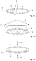
- a cover plate 2 is provided, the surface 4 of which typically corresponds to the dimensions of a semiconductor wafer. In other embodiments, however, it can also be provided that the size of the cover plate 2 is selected to be smaller, for example, so that a semiconductor wafer is only partially covered.
- a plasma rod 6 is arranged on the surface 4 of the cover plate 2 and can ionize the area between the surface 4 and the plasma rod 6 by means of suitable electrodes, so that a plasma rod 6 is not in Figure 1A shown carrier gas is ionized and then deposited on the surface 4. Consequently, if as in Fig.
- the cover plate 2 is pulled one or more times under the plasma rod 6, a functional layer 10, the thickness of which can be influenced by the process control, ie the number and speed of the passages of the cover plate 2 under the plasma rod 6.
- the functional layer 10 is initially inactive after the plasma treatment.
- the functional layer 10 which is formed over the entire area on the surface 4 of the cover pane 2, can be activated by means of light from a light source 12.
- the light source 12 which emits light 14 in the near UV range, for example, activates the functional layer 10 under appropriately selected exposure conditions.
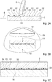
- a semiconductor wafer 16 is now provided, whereby by immediately bringing the cover plate 2 and the semiconductor wafer 16 into contact, a bonding process is generated between an upper side 20 of the semiconductor wafer 16 and the functional layer 10 of the cover plate 2, the areal contact covalent bonds of the activated functional layer and the top 20 of the semiconductor wafer 16 arise. These covalent bonds lead to a permanent chemical bond between the cover plate 2 and the semiconductor wafer 16.
- the contact between the cover plate 2 and the semiconductor wafer 16 is shown on the basis of the displacement directions 18 and 18 'in FIG Figure 1C indicated.
- the cover plate 2 is structured on its surface 4, so that corresponding structural elements 22 have been created, between which cavities 24 are formed.
- the structuring with the structural elements 22 can take place in the form of a grid.
- the functional layer 10 is in turn formed by movement along the directional arrow 8.
- the activation of the functional layer 10 takes place in a process chamber 26 into which the cover panel 2, the Semiconductor wafer 16 and the light source 12 are arranged.
- a chemical composite of cover plate 2 and semiconductor wafer 16 can be created in the area of the cavities by contacting based on the movement along the displacement directions 18 and 18 ' 24 gas with a desired composition or density is present.
- Fig. 2 shown enlarged again. It can be seen that a defined atmosphere prevails in the cavities 24, which are delimited by the structural elements 22, so that the components indicated by the reference numeral 28 are surrounded by the defined gas atmosphere in the cavity 24.
- a defined atmosphere prevails in the cavities 24, which are delimited by the structural elements 22, so that the components indicated by the reference numeral 28 are surrounded by the defined gas atmosphere in the cavity 24.
- Such a procedure can be used both in high-frequency electronics to reduce power losses and in microsystem technology to produce cavities required for sensors.
- a reference pressure chamber in the case of an absolute pressure sensor or a negative pressure chamber of a rotation rate sensor can be provided.
- a cavity filled with gas is also advantageous.
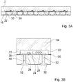
- FIG. 3A It is shown that the semiconductor wafer 16 is thinned from a side opposite the top side 20, so that rear-side metallizations and contacts can be formed. These can lead the components 28 to rear-side electrodes 32 via corresponding vias 30.
- a finished electronic component is obtained which is hermetically shielded and sealed against the environment via the housing 34 formed from the material of the cover plate 2.
- the separation is preferably carried out in such a way that the structural elements 22 are partially retained. Areas in which connections have been made by means of active surface bonding are shown schematically with the reference numeral 36 in FIG Figure 3B indicated.
- the cavity 24 can be filled with gas.
- the cover plate 2 can be used as a carrier when processing the rear side of the semiconductor wafer 16 in order to produce vias in the semiconductor wafer 16 or to thin the semiconductor wafer 16.
Landscapes
- Engineering & Computer Science (AREA)
- Microelectronics & Electronic Packaging (AREA)
- Manufacturing & Machinery (AREA)
- Micromachines (AREA)
- Container, Conveyance, Adherence, Positioning, Of Wafer (AREA)
Claims (9)
- Procédé de fabrication d'une plaquette de semi-conducteur (16) au moins partiellement encapsulée, comprenant les étapes suivantes :- fournir une plaquette de semi-conducteur (16) comportant des composants (28) sur son côté supérieur (20),- fournir un disque de recouvrement (2) dont la surface (4) recouvre au moins partiellement la plaquette de semi-conducteur (16),- fonctionnaliser la surface (4) du disque de recouvrement (2) pour former une couche (10) fonctionnelle par traitement par plasma de la surface (4) du disque de recouvrement (2),- rapprocher, immédiatement après l'activation de la couche (10) fonctionnelle par exposition à la lumière, le côté supérieur (20) de la plaquette de semi-conducteur (16) et la surface (4) du disque de recouvrement (2) de façon à lier chimiquement la plaquette de semi-conducteur (16) et le disque de recouvrement (2), de sorte que le disque de recouvrement (2) forme un boîtier pour la plaquette de semi-conducteur (16).
- Procédé selon la revendication 1, selon lequel le traitement par plasma comprend le déplacement de la surface (4) du disque de recouvrement (2) sous un barreau de plasma (6), le nombre et la vitesse des mouvements du disque de recouvrement (2) sous le barreau de plasma (6) définissant une épaisseur de la couche (10) fonctionnelle.
- Procédé selon l'une des revendications 1 ou 2, selon lequel l'activation de la couche (10) fonctionnelle comprend une exposition à une lumière (14) d'une longueur d'onde prédéterminée, de préférence dans le domaine de l'UV.
- Procédé selon l'une des revendications 1 à 3, selon lequel les étapes de processus sont réalisées dans une chambre de traitement (26) étanche, une composition et une pression d'une atmosphère gazeuse pouvant être réglées lors de l'activation de la couche (10) fonctionnelle et de l'assemblage des disques (2, 16).
- Procédé selon l'une des revendications 1 à 4, selon lequel le disque de recouvrement (2) est structuré sur son côté supérieur (20) tourné vers la plaquette de semi-conducteur (16), de sorte que des groupes de composants individuels sur le côté supérieur (20) de la plaquette de semi-conducteur (16) sont disposés dans des cavités (24) sur la surface (4) du disque de recouvrement (2).
- Procédé selon l'une des revendications 1 à 5, selon lequel la plaquette de semi-conducteur (16) est amincie du côté opposé au côté supérieur (20), et peut ensuite être mise en contact depuis le côté arrière.
- Procédé selon la revendication 6, selon lequel il est réalisé une séparation, de préférence par sciage, d'ensembles individuels, de préférence le long d'éléments structuraux (22) sur le disque de recouvrement (2).
- Procédé selon l'une des revendications 1 à 7, selon lequel les composants (28) de la plaquette de semi-conducteur (16) se présentent sous la forme de composants microélectroniques ou micromécaniques qui sont reliés à des composantes électroniques, de préférence des composantes haute fréquence.
- Procédé selon l'une des revendications 1 à 8, selon lequel le disque de recouvrement (2) est utilisé comme support pendant le traitement du côté arrière de la plaquette de semi-conducteur (16).
Applications Claiming Priority (2)
| Application Number | Priority Date | Filing Date | Title |
|---|---|---|---|
| DE102018111200.9A DE102018111200A1 (de) | 2018-05-09 | 2018-05-09 | Verfahren zur Herstellung eines wenigstens teilweise gehäusten Halbleiterwafers |
| PCT/EP2019/061359 WO2019215027A1 (fr) | 2018-05-09 | 2019-05-03 | Procédé servant à fabriquer une tranche semi-conductrice au moins en partie encapsulée |
Publications (2)
| Publication Number | Publication Date |
|---|---|
| EP3601154A1 EP3601154A1 (fr) | 2020-02-05 |
| EP3601154B1 true EP3601154B1 (fr) | 2020-11-11 |
Family
ID=66429380
Family Applications (1)
| Application Number | Title | Priority Date | Filing Date |
|---|---|---|---|
| EP19722096.5A Active EP3601154B1 (fr) | 2018-05-09 | 2019-05-03 | Procédé servant à fabriquer une tranche semi-conductrice au moins en partie encapsulée |
Country Status (7)
| Country | Link |
|---|---|
| US (1) | US11018029B2 (fr) |
| EP (1) | EP3601154B1 (fr) |
| JP (1) | JP2021521627A (fr) |
| CN (1) | CN112119032B (fr) |
| DE (1) | DE102018111200A1 (fr) |
| TW (1) | TWI732212B (fr) |
| WO (1) | WO2019215027A1 (fr) |
Families Citing this family (1)
| Publication number | Priority date | Publication date | Assignee | Title |
|---|---|---|---|---|
| JP7529777B2 (ja) * | 2019-12-19 | 2024-08-06 | エーファウ・グループ・エー・タルナー・ゲーエムベーハー | カプセル化されて個別化された構成要素およびカプセル化されて個別化された構成要素を製造する方法 |
Family Cites Families (16)
| Publication number | Priority date | Publication date | Assignee | Title |
|---|---|---|---|---|
| DE10209423A1 (de) * | 2002-03-05 | 2003-09-18 | Schwerionenforsch Gmbh | Beschichtung aus einer Gettermetall-Legierung sowie Anordnung und Verfahren zur Herstellung derselben |
| US6822326B2 (en) * | 2002-09-25 | 2004-11-23 | Ziptronix | Wafer bonding hermetic encapsulation |
| DE10256693A1 (de) * | 2002-12-04 | 2004-06-24 | Süss Microtec Lithography Gmbh | Verfahren und Vorrichtung zur Oberflächenmodifizierung und zum Bonden von Halbleitersubstraten mittels atmosphärischer Plasmabehandlung |
| DE102004008699B3 (de) * | 2004-02-23 | 2005-10-06 | Süss Microtec Lithography Gmbh | Verfahren und Vorrichtung zur Vorbehandlung der Oberflächen von zu bondenden Substraten |
| FR2880184B1 (fr) | 2004-12-28 | 2007-03-30 | Commissariat Energie Atomique | Procede de detourage d'une structure obtenue par assemblage de deux plaques |
| TWI319602B (en) * | 2007-01-10 | 2010-01-11 | Advanced Semiconductor Eng | Releasing structure of a controllable cap and releasing method thereof |
| JP2009035720A (ja) * | 2007-07-11 | 2009-02-19 | Seiko Epson Corp | 接合膜付き基材、接合方法および接合体 |
| DE102009020163B4 (de) * | 2009-05-07 | 2012-07-19 | Fraunhofer-Gesellschaft zur Förderung der angewandten Forschung e.V. | Verfahren zum zwischenschichtfreien Verbinden von Substraten, Vorrichtung zur Durchführung einer Plasmabehandlung sowie deren Verwendung |
| US9045332B2 (en) | 2011-11-29 | 2015-06-02 | Qualcomm Mems Technologies, Inc. | Thin back glass interconnect |
| JP5934078B2 (ja) * | 2012-11-19 | 2016-06-15 | 信越化学工業株式会社 | 繊維含有樹脂基板及び半導体装置の製造方法 |
| JP6314983B2 (ja) * | 2013-06-27 | 2018-04-25 | 三菱ケミカル株式会社 | 偏光素子、及び偏光素子の製造方法 |
| US9522822B2 (en) * | 2014-05-13 | 2016-12-20 | Taiwan Semiconductor Manufacturing Co., Ltd. | Sensor integration with an outgassing barrier and a stable electrical signal path |
| JP6165686B2 (ja) * | 2014-07-31 | 2017-07-19 | 信越化学工業株式会社 | 支持基材付封止材、封止後半導体素子搭載基板、封止後半導体素子形成ウエハ、半導体装置、及び半導体装置の製造方法 |
| US9574959B2 (en) * | 2014-09-02 | 2017-02-21 | Apple Inc. | Various stress free sensor packages using wafer level supporting die and air gap technique |
| CN104821376A (zh) * | 2015-04-24 | 2015-08-05 | 京东方科技集团股份有限公司 | 一种oled面板及其制造方法、显示装置 |
| JP6454606B2 (ja) * | 2015-06-02 | 2019-01-16 | 信越化学工業株式会社 | 酸化物単結晶薄膜を備えた複合ウェーハの製造方法 |
-
2018
- 2018-05-09 DE DE102018111200.9A patent/DE102018111200A1/de not_active Withdrawn
-
2019
- 2019-05-03 WO PCT/EP2019/061359 patent/WO2019215027A1/fr not_active Ceased
- 2019-05-03 EP EP19722096.5A patent/EP3601154B1/fr active Active
- 2019-05-03 CN CN201980014632.4A patent/CN112119032B/zh active Active
- 2019-05-03 JP JP2020551911A patent/JP2021521627A/ja active Pending
- 2019-05-03 US US16/971,849 patent/US11018029B2/en active Active
- 2019-05-06 TW TW108115555A patent/TWI732212B/zh active
Non-Patent Citations (1)
| Title |
|---|
| None * |
Also Published As
| Publication number | Publication date |
|---|---|
| US11018029B2 (en) | 2021-05-25 |
| TW202004927A (zh) | 2020-01-16 |
| CN112119032A (zh) | 2020-12-22 |
| EP3601154A1 (fr) | 2020-02-05 |
| DE102018111200A1 (de) | 2019-11-14 |
| WO2019215027A1 (fr) | 2019-11-14 |
| CN112119032B (zh) | 2024-11-26 |
| JP2021521627A (ja) | 2021-08-26 |
| TWI732212B (zh) | 2021-07-01 |
| US20210013052A1 (en) | 2021-01-14 |
Similar Documents
| Publication | Publication Date | Title |
|---|---|---|
| EP1866236B1 (fr) | Composant micromecanique, et son procede de production | |
| EP2170763B1 (fr) | Procédé de production d'un composant, et composant obtenu | |
| EP1836123B1 (fr) | Procede pour produire une pression interne predeterminee dans une cavite d'un composant a semi-conducteur | |
| DE102011102266B4 (de) | Anordnung mit einem MEMS-Bauelement mit einer PFPE Schicht und Verfahren zur Herstellung | |
| DE102013217349B4 (de) | Mikromechanische Sensoranordnung und entsprechendes Herstellungsverfahren | |
| DE102011103516B4 (de) | Verfahren zum Befüllen eines Hohlraums mit einer Atmosphäre | |
| EP1869705B1 (fr) | Procédé de fabrication de dispositifs électroniques en boîtier et dispositif électronique en boîtier | |
| DE102012206869A1 (de) | Mikromechanisches Bauelement und Verfahren zur Herstellung eines mikromechanischen Bauelements | |
| DE102013222733A1 (de) | Mikromechanische Sensorvorrichtung | |
| DE102012112058A1 (de) | MEMS-Bauelement und Verfahren zur Verkapselung von MEMS-Bauelementen | |
| DE102010001711A1 (de) | Halbleiter-Bauelement und entsprechendes Herstellungsverfahren | |
| DE102010056562B4 (de) | Elektroakustisches Bauelement und Verfahren zur Herstellung des elektroakustischen Bauelements | |
| DE102011086765A1 (de) | Chip mit mikro-elektromechanischer Struktur und Verfahren zum Herstellen eines Chips mit mikro-elektromechanischer Struktur | |
| WO2020178135A1 (fr) | Dispositif formant capteur micromécanique et procédé de fabrication correspondant | |
| EP3526158A1 (fr) | Procédé pour produire un capteur de pression micromécanique découplé de contraintes | |
| EP3601154B1 (fr) | Procédé servant à fabriquer une tranche semi-conductrice au moins en partie encapsulée | |
| DE102018125378B3 (de) | Anodisches Bonden eines Glassubstrats mit Kontaktdurchführungen an ein Siliziumsubstrat | |
| DE102006040115A1 (de) | Verfahren und Anordnung zur hermetisch dichten vertikalen elektrischen Durchkontaktierung von Deckscheiben der Mikrosystemtechnik | |
| DE10324421B4 (de) | Halbleiterbauelement mit Metallisierungsfläche und Verfahren zur Herstellung desselben | |
| DE10232190A1 (de) | Verfahren zur Herstellung eines Bauelements mit tiefliegenden Anschlußflächen | |
| DE102007001290A1 (de) | Halbleitermodul | |
| DE102010030457A1 (de) | Verfahren zur Herstellung von gehäusten mikromechanischen Bauelementen und entsprechendes gehäustes mikromechanisches Bauelement | |
| DE102014204035B4 (de) | Hybrid integriertes Bauteil mit definiert vorgegebenen Innendruck im MEM Hohlraum und Verfahren zu dessen Herstellung | |
| DE102021204645A1 (de) | Verfahren zur Herstellung eines mikroelektromechanischen Sensors aus einem MEMS-Element und einem ASIC-Element und mikroelektromechanischer Sensor | |
| DE19710375C2 (de) | Verfahren zum Herstellen von räumlich strukturierten Bauteilen |
Legal Events
| Date | Code | Title | Description |
|---|---|---|---|
| STAA | Information on the status of an ep patent application or granted ep patent |
Free format text: STATUS: UNKNOWN |
|
| STAA | Information on the status of an ep patent application or granted ep patent |
Free format text: STATUS: THE INTERNATIONAL PUBLICATION HAS BEEN MADE |
|
| PUAI | Public reference made under article 153(3) epc to a published international application that has entered the european phase |
Free format text: ORIGINAL CODE: 0009012 |
|
| STAA | Information on the status of an ep patent application or granted ep patent |
Free format text: STATUS: REQUEST FOR EXAMINATION WAS MADE |
|
| 17P | Request for examination filed |
Effective date: 20191029 |
|
| AK | Designated contracting states |
Kind code of ref document: A1 Designated state(s): AL AT BE BG CH CY CZ DE DK EE ES FI FR GB GR HR HU IE IS IT LI LT LU LV MC MK MT NL NO PL PT RO RS SE SI SK SM TR |
|
| AX | Request for extension of the european patent |
Extension state: BA ME |
|
| STAA | Information on the status of an ep patent application or granted ep patent |
Free format text: STATUS: EXAMINATION IS IN PROGRESS |
|
| 17Q | First examination report despatched |
Effective date: 20200302 |
|
| GRAP | Despatch of communication of intention to grant a patent |
Free format text: ORIGINAL CODE: EPIDOSNIGR1 |
|
| STAA | Information on the status of an ep patent application or granted ep patent |
Free format text: STATUS: GRANT OF PATENT IS INTENDED |
|
| GRAS | Grant fee paid |
Free format text: ORIGINAL CODE: EPIDOSNIGR3 |
|
| GRAA | (expected) grant |
Free format text: ORIGINAL CODE: 0009210 |
|
| STAA | Information on the status of an ep patent application or granted ep patent |
Free format text: STATUS: THE PATENT HAS BEEN GRANTED |
|
| DAV | Request for validation of the european patent (deleted) | ||
| DAX | Request for extension of the european patent (deleted) | ||
| INTG | Intention to grant announced |
Effective date: 20200914 |
|
| AK | Designated contracting states |
Kind code of ref document: B1 Designated state(s): AL AT BE BG CH CY CZ DE DK EE ES FI FR GB GR HR HU IE IS IT LI LT LU LV MC MK MT NL NO PL PT RO RS SE SI SK SM TR |
|
| REG | Reference to a national code |
Ref country code: GB Ref legal event code: FG4D Free format text: NOT ENGLISH |
|
| REG | Reference to a national code |
Ref country code: CH Ref legal event code: EP |
|
| REG | Reference to a national code |
Ref country code: AT Ref legal event code: REF Ref document number: 1333278 Country of ref document: AT Kind code of ref document: T Effective date: 20201115 |
|
| REG | Reference to a national code |
Ref country code: DE Ref legal event code: R096 Ref document number: 502019000403 Country of ref document: DE |
|
| REG | Reference to a national code |
Ref country code: IE Ref legal event code: FG4D Free format text: LANGUAGE OF EP DOCUMENT: GERMAN |
|
| PG25 | Lapsed in a contracting state [announced via postgrant information from national office to epo] |
Ref country code: GR Free format text: LAPSE BECAUSE OF FAILURE TO SUBMIT A TRANSLATION OF THE DESCRIPTION OR TO PAY THE FEE WITHIN THE PRESCRIBED TIME-LIMIT Effective date: 20210212 Ref country code: NO Free format text: LAPSE BECAUSE OF FAILURE TO SUBMIT A TRANSLATION OF THE DESCRIPTION OR TO PAY THE FEE WITHIN THE PRESCRIBED TIME-LIMIT Effective date: 20210211 Ref country code: PT Free format text: LAPSE BECAUSE OF FAILURE TO SUBMIT A TRANSLATION OF THE DESCRIPTION OR TO PAY THE FEE WITHIN THE PRESCRIBED TIME-LIMIT Effective date: 20210311 Ref country code: RS Free format text: LAPSE BECAUSE OF FAILURE TO SUBMIT A TRANSLATION OF THE DESCRIPTION OR TO PAY THE FEE WITHIN THE PRESCRIBED TIME-LIMIT Effective date: 20201111 Ref country code: FI Free format text: LAPSE BECAUSE OF FAILURE TO SUBMIT A TRANSLATION OF THE DESCRIPTION OR TO PAY THE FEE WITHIN THE PRESCRIBED TIME-LIMIT Effective date: 20201111 |
|
| PG25 | Lapsed in a contracting state [announced via postgrant information from national office to epo] |
Ref country code: BG Free format text: LAPSE BECAUSE OF FAILURE TO SUBMIT A TRANSLATION OF THE DESCRIPTION OR TO PAY THE FEE WITHIN THE PRESCRIBED TIME-LIMIT Effective date: 20210211 Ref country code: SE Free format text: LAPSE BECAUSE OF FAILURE TO SUBMIT A TRANSLATION OF THE DESCRIPTION OR TO PAY THE FEE WITHIN THE PRESCRIBED TIME-LIMIT Effective date: 20201111 Ref country code: LV Free format text: LAPSE BECAUSE OF FAILURE TO SUBMIT A TRANSLATION OF THE DESCRIPTION OR TO PAY THE FEE WITHIN THE PRESCRIBED TIME-LIMIT Effective date: 20201111 Ref country code: PL Free format text: LAPSE BECAUSE OF FAILURE TO SUBMIT A TRANSLATION OF THE DESCRIPTION OR TO PAY THE FEE WITHIN THE PRESCRIBED TIME-LIMIT Effective date: 20201111 Ref country code: IS Free format text: LAPSE BECAUSE OF FAILURE TO SUBMIT A TRANSLATION OF THE DESCRIPTION OR TO PAY THE FEE WITHIN THE PRESCRIBED TIME-LIMIT Effective date: 20210311 |
|
| REG | Reference to a national code |
Ref country code: LT Ref legal event code: MG9D |
|
| PG25 | Lapsed in a contracting state [announced via postgrant information from national office to epo] |
Ref country code: HR Free format text: LAPSE BECAUSE OF FAILURE TO SUBMIT A TRANSLATION OF THE DESCRIPTION OR TO PAY THE FEE WITHIN THE PRESCRIBED TIME-LIMIT Effective date: 20201111 |
|
| PG25 | Lapsed in a contracting state [announced via postgrant information from national office to epo] |
Ref country code: SM Free format text: LAPSE BECAUSE OF FAILURE TO SUBMIT A TRANSLATION OF THE DESCRIPTION OR TO PAY THE FEE WITHIN THE PRESCRIBED TIME-LIMIT Effective date: 20201111 Ref country code: SK Free format text: LAPSE BECAUSE OF FAILURE TO SUBMIT A TRANSLATION OF THE DESCRIPTION OR TO PAY THE FEE WITHIN THE PRESCRIBED TIME-LIMIT Effective date: 20201111 Ref country code: EE Free format text: LAPSE BECAUSE OF FAILURE TO SUBMIT A TRANSLATION OF THE DESCRIPTION OR TO PAY THE FEE WITHIN THE PRESCRIBED TIME-LIMIT Effective date: 20201111 Ref country code: CZ Free format text: LAPSE BECAUSE OF FAILURE TO SUBMIT A TRANSLATION OF THE DESCRIPTION OR TO PAY THE FEE WITHIN THE PRESCRIBED TIME-LIMIT Effective date: 20201111 Ref country code: RO Free format text: LAPSE BECAUSE OF FAILURE TO SUBMIT A TRANSLATION OF THE DESCRIPTION OR TO PAY THE FEE WITHIN THE PRESCRIBED TIME-LIMIT Effective date: 20201111 Ref country code: LT Free format text: LAPSE BECAUSE OF FAILURE TO SUBMIT A TRANSLATION OF THE DESCRIPTION OR TO PAY THE FEE WITHIN THE PRESCRIBED TIME-LIMIT Effective date: 20201111 |
|
| REG | Reference to a national code |
Ref country code: DE Ref legal event code: R097 Ref document number: 502019000403 Country of ref document: DE |
|
| PG25 | Lapsed in a contracting state [announced via postgrant information from national office to epo] |
Ref country code: DK Free format text: LAPSE BECAUSE OF FAILURE TO SUBMIT A TRANSLATION OF THE DESCRIPTION OR TO PAY THE FEE WITHIN THE PRESCRIBED TIME-LIMIT Effective date: 20201111 |
|
| PLBE | No opposition filed within time limit |
Free format text: ORIGINAL CODE: 0009261 |
|
| STAA | Information on the status of an ep patent application or granted ep patent |
Free format text: STATUS: NO OPPOSITION FILED WITHIN TIME LIMIT |
|
| REG | Reference to a national code |
Ref country code: NL Ref legal event code: FP |
|
| 26N | No opposition filed |
Effective date: 20210812 |
|
| PG25 | Lapsed in a contracting state [announced via postgrant information from national office to epo] |
Ref country code: AL Free format text: LAPSE BECAUSE OF FAILURE TO SUBMIT A TRANSLATION OF THE DESCRIPTION OR TO PAY THE FEE WITHIN THE PRESCRIBED TIME-LIMIT Effective date: 20201111 |
|
| PG25 | Lapsed in a contracting state [announced via postgrant information from national office to epo] |
Ref country code: SI Free format text: LAPSE BECAUSE OF FAILURE TO SUBMIT A TRANSLATION OF THE DESCRIPTION OR TO PAY THE FEE WITHIN THE PRESCRIBED TIME-LIMIT Effective date: 20201111 |
|
| PG25 | Lapsed in a contracting state [announced via postgrant information from national office to epo] |
Ref country code: LU Free format text: LAPSE BECAUSE OF NON-PAYMENT OF DUE FEES Effective date: 20210503 Ref country code: MC Free format text: LAPSE BECAUSE OF FAILURE TO SUBMIT A TRANSLATION OF THE DESCRIPTION OR TO PAY THE FEE WITHIN THE PRESCRIBED TIME-LIMIT Effective date: 20201111 Ref country code: ES Free format text: LAPSE BECAUSE OF FAILURE TO SUBMIT A TRANSLATION OF THE DESCRIPTION OR TO PAY THE FEE WITHIN THE PRESCRIBED TIME-LIMIT Effective date: 20201111 |
|
| REG | Reference to a national code |
Ref country code: BE Ref legal event code: MM Effective date: 20210531 |
|
| PG25 | Lapsed in a contracting state [announced via postgrant information from national office to epo] |
Ref country code: IE Free format text: LAPSE BECAUSE OF NON-PAYMENT OF DUE FEES Effective date: 20210503 |
|
| PG25 | Lapsed in a contracting state [announced via postgrant information from national office to epo] |
Ref country code: IS Free format text: LAPSE BECAUSE OF FAILURE TO SUBMIT A TRANSLATION OF THE DESCRIPTION OR TO PAY THE FEE WITHIN THE PRESCRIBED TIME-LIMIT Effective date: 20210311 |
|
| PG25 | Lapsed in a contracting state [announced via postgrant information from national office to epo] |
Ref country code: BE Free format text: LAPSE BECAUSE OF NON-PAYMENT OF DUE FEES Effective date: 20210531 |
|
| REG | Reference to a national code |
Ref country code: CH Ref legal event code: PL |
|
| PG25 | Lapsed in a contracting state [announced via postgrant information from national office to epo] |
Ref country code: LI Free format text: LAPSE BECAUSE OF NON-PAYMENT OF DUE FEES Effective date: 20220531 Ref country code: CH Free format text: LAPSE BECAUSE OF NON-PAYMENT OF DUE FEES Effective date: 20220531 |
|
| PG25 | Lapsed in a contracting state [announced via postgrant information from national office to epo] |
Ref country code: CY Free format text: LAPSE BECAUSE OF FAILURE TO SUBMIT A TRANSLATION OF THE DESCRIPTION OR TO PAY THE FEE WITHIN THE PRESCRIBED TIME-LIMIT Effective date: 20201111 |
|
| PG25 | Lapsed in a contracting state [announced via postgrant information from national office to epo] |
Ref country code: HU Free format text: LAPSE BECAUSE OF FAILURE TO SUBMIT A TRANSLATION OF THE DESCRIPTION OR TO PAY THE FEE WITHIN THE PRESCRIBED TIME-LIMIT; INVALID AB INITIO Effective date: 20190503 |
|
| PG25 | Lapsed in a contracting state [announced via postgrant information from national office to epo] |
Ref country code: MK Free format text: LAPSE BECAUSE OF FAILURE TO SUBMIT A TRANSLATION OF THE DESCRIPTION OR TO PAY THE FEE WITHIN THE PRESCRIBED TIME-LIMIT Effective date: 20201111 |
|
| PG25 | Lapsed in a contracting state [announced via postgrant information from national office to epo] |
Ref country code: MT Free format text: LAPSE BECAUSE OF FAILURE TO SUBMIT A TRANSLATION OF THE DESCRIPTION OR TO PAY THE FEE WITHIN THE PRESCRIBED TIME-LIMIT Effective date: 20201111 |
|
| PGFP | Annual fee paid to national office [announced via postgrant information from national office to epo] |
Ref country code: NL Payment date: 20250522 Year of fee payment: 7 |
|
| PGFP | Annual fee paid to national office [announced via postgrant information from national office to epo] |
Ref country code: DE Payment date: 20250531 Year of fee payment: 7 |
|
| PGFP | Annual fee paid to national office [announced via postgrant information from national office to epo] |
Ref country code: GB Payment date: 20250522 Year of fee payment: 7 |
|
| PGFP | Annual fee paid to national office [announced via postgrant information from national office to epo] |
Ref country code: IT Payment date: 20250530 Year of fee payment: 7 |
|
| REG | Reference to a national code |
Ref country code: AT Ref legal event code: MM01 Ref document number: 1333278 Country of ref document: AT Kind code of ref document: T Effective date: 20240503 |
|
| PGFP | Annual fee paid to national office [announced via postgrant information from national office to epo] |
Ref country code: FR Payment date: 20250526 Year of fee payment: 7 |
|
| PG25 | Lapsed in a contracting state [announced via postgrant information from national office to epo] |
Ref country code: AT Free format text: LAPSE BECAUSE OF NON-PAYMENT OF DUE FEES Effective date: 20240503 |
|
| PG25 | Lapsed in a contracting state [announced via postgrant information from national office to epo] |
Ref country code: TR Free format text: LAPSE BECAUSE OF FAILURE TO SUBMIT A TRANSLATION OF THE DESCRIPTION OR TO PAY THE FEE WITHIN THE PRESCRIBED TIME-LIMIT Effective date: 20201111 |
|
| PGFP | Annual fee paid to national office [announced via postgrant information from national office to epo] |
Ref country code: AT Payment date: 20260410 Year of fee payment: 5 |