EP3605151A1 - Détecteur de comptage de photons - Google Patents
Détecteur de comptage de photons Download PDFInfo
- Publication number
- EP3605151A1 EP3605151A1 EP18186822.5A EP18186822A EP3605151A1 EP 3605151 A1 EP3605151 A1 EP 3605151A1 EP 18186822 A EP18186822 A EP 18186822A EP 3605151 A1 EP3605151 A1 EP 3605151A1
- Authority
- EP
- European Patent Office
- Prior art keywords
- direct conversion
- absorption
- conversion layer
- count signal
- layer
- Prior art date
- Legal status (The legal status is an assumption and is not a legal conclusion. Google has not performed a legal analysis and makes no representation as to the accuracy of the status listed.)
- Withdrawn
Links
- 238000006243 chemical reaction Methods 0.000 claims abstract description 162
- 238000010521 absorption reaction Methods 0.000 claims abstract description 83
- 239000000463 material Substances 0.000 claims abstract description 79
- 230000005670 electromagnetic radiation Effects 0.000 claims abstract description 44
- 238000012545 processing Methods 0.000 claims abstract description 33
- 238000012937 correction Methods 0.000 claims description 39
- 230000008859 change Effects 0.000 claims description 13
- JBRZTFJDHDCESZ-UHFFFAOYSA-N AsGa Chemical compound [As]#[Ga] JBRZTFJDHDCESZ-UHFFFAOYSA-N 0.000 claims description 12
- 229910001218 Gallium arsenide Inorganic materials 0.000 claims description 12
- 238000001514 detection method Methods 0.000 claims description 10
- 238000000034 method Methods 0.000 claims description 10
- 238000004590 computer program Methods 0.000 claims description 6
- 229910052710 silicon Inorganic materials 0.000 claims description 3
- 239000010703 silicon Substances 0.000 claims description 3
- MARUHZGHZWCEQU-UHFFFAOYSA-N 5-phenyl-2h-tetrazole Chemical compound C1=CC=CC=C1C1=NNN=N1 MARUHZGHZWCEQU-UHFFFAOYSA-N 0.000 claims description 2
- GPXJNWSHGFTCBW-UHFFFAOYSA-N Indium phosphide Chemical compound [In]#P GPXJNWSHGFTCBW-UHFFFAOYSA-N 0.000 claims description 2
- XUIMIQQOPSSXEZ-UHFFFAOYSA-N Silicon Chemical compound [Si] XUIMIQQOPSSXEZ-UHFFFAOYSA-N 0.000 claims description 2
- QWUZMTJBRUASOW-UHFFFAOYSA-N cadmium tellanylidenezinc Chemical compound [Zn].[Cd].[Te] QWUZMTJBRUASOW-UHFFFAOYSA-N 0.000 claims description 2
- 229960003671 mercuric iodide Drugs 0.000 claims description 2
- YFDLHELOZYVNJE-UHFFFAOYSA-L mercury diiodide Chemical compound I[Hg]I YFDLHELOZYVNJE-UHFFFAOYSA-L 0.000 claims description 2
- 239000010410 layer Substances 0.000 description 167
- 238000005259 measurement Methods 0.000 description 14
- 238000010586 diagram Methods 0.000 description 7
- 230000004907 flux Effects 0.000 description 7
- 230000005855 radiation Effects 0.000 description 6
- 230000000875 corresponding effect Effects 0.000 description 5
- 238000000354 decomposition reaction Methods 0.000 description 5
- 230000001419 dependent effect Effects 0.000 description 3
- 238000002059 diagnostic imaging Methods 0.000 description 2
- 238000012804 iterative process Methods 0.000 description 2
- 229910000679 solder Inorganic materials 0.000 description 2
- 230000003595 spectral effect Effects 0.000 description 2
- 239000000758 substrate Substances 0.000 description 2
- 239000011701 zinc Substances 0.000 description 2
- 229910004613 CdTe Inorganic materials 0.000 description 1
- 230000008901 benefit Effects 0.000 description 1
- 238000004891 communication Methods 0.000 description 1
- 238000002591 computed tomography Methods 0.000 description 1
- 230000002596 correlated effect Effects 0.000 description 1
- 239000002355 dual-layer Substances 0.000 description 1
- 238000005516 engineering process Methods 0.000 description 1
- 238000003384 imaging method Methods 0.000 description 1
- 238000004806 packaging method and process Methods 0.000 description 1
- 238000001228 spectrum Methods 0.000 description 1
Images



Classifications
-
- G—PHYSICS
- G01—MEASURING; TESTING
- G01T—MEASUREMENT OF NUCLEAR OR X-RADIATION
- G01T1/00—Measuring X-radiation, gamma radiation, corpuscular radiation, or cosmic radiation
- G01T1/16—Measuring radiation intensity
- G01T1/24—Measuring radiation intensity with semiconductor detectors
- G01T1/242—Stacked detectors, e.g. for depth information
-
- G—PHYSICS
- G01—MEASURING; TESTING
- G01T—MEASUREMENT OF NUCLEAR OR X-RADIATION
- G01T1/00—Measuring X-radiation, gamma radiation, corpuscular radiation, or cosmic radiation
- G01T1/29—Measurement performed on radiation beams, e.g. position or section of the beam; Measurement of spatial distribution of radiation
- G01T1/2914—Measurement of spatial distribution of radiation
- G01T1/2921—Static instruments for imaging the distribution of radioactivity in one or two dimensions; Radio-isotope cameras
- G01T1/2928—Static instruments for imaging the distribution of radioactivity in one or two dimensions; Radio-isotope cameras using solid state detectors
Definitions
- the present invention relates to a photon counting detector and a correction device and method for a photon counting detector.
- the present invention relates further to a photon counting detection arrangement.
- US 2008/230709 A1 discloses a diagnostic imaging system including a high frequency electromagnetic energy source that emits a beam of high frequency electromagnetic energy toward an object to be imaged.
- An energy discriminating (ED) detector receives high frequency electromagnetic energy emitted by the high frequency electromagnetic energy source.
- the ED detector includes a first direct conversion layer and a second direct conversion layer.
- the first direct conversion layer comprises a first direct conversion material
- the second direct conversion layer comprises a second direct conversion material that is different from the first direct conversion material.
- a data acquisition system (DAS) is operably connected to the ED detector and a computer operably connected to the DAS.
- DAS data acquisition system
- a photon counting detector comprising
- a correction device for a photon counting detector comprising
- a photon counting detection arrangement comprising:
- a computer program which comprises program code means for causing a computer to perform the steps of the method disclosed herein when said computer program is carried out on a computer as well as a non-transitory computer-readable recording medium that stores therein a computer program product, which, when executed by a processor, causes the method disclosed herein to be performed.
- the present invention is based on the idea to segment the detection volume into two distinct, preferably energy resolving layers.
- the first (with respect to the incident radiation higher/top) layer is intended to be a low absorption layer material, however with high stability performance.
- the second (with respect to the incident radiation lower) layer comprises a high absorption material.
- the top layer which only sees a fraction of the total flux, serves as reference to correct the stability issues of the lower layer, but may in addition provide energy-resolving information.
- the first layer with low absorption may e.g. be made of GaAs or Si. GaAs is a very stable material, which is however inadequate for CT as a stand-alone detector due to its low absorption.
- the second layer with high absorption may e.g. be made of Cd(Zn)Te (CZT) or CdTe, which is known to still offer insufficient stability for the stringent requirements of clinical CT, but provides sufficient absorption.
- a single ASIC substrate may be used to serve as carrier for both layers and for carrying processing circuitry for correcting, based on the first count signal of the first layer, the second count signal of the second count signal for errors caused mainly by the insufficient stability of the second layer.
- the processing circuitry is configured to correct the second count signal for errors caused by lower stability of the high-absorption direct conversion material compared to the low-absorption direction conversion material.
- the disclosed photon counting detector With the disclosed photon counting detector, the deviation of the second count signal from the expected number of counts can be compensated.
- High-energy electromagnetic radiation shall generally be understood as electromagnetic radiation having energies above e.g. 1 keV, preferably having reasonable clinically relevant energies, e.g. in the range above 20 keV (preferably up to e.g. 160 keV).
- This electromagnetic radiation is preferably x-ray radiation, but may generally also be gamma radiation.
- said low-absorption direct conversion material is configured for converting high-energy electromagnetic radiation into one or more first energy-resolving count signals and said high-absorption direct conversion material is configured for converting high-energy electromagnetic radiation into one or more second energy-resolving count signals.
- This provides energy-resolved information. Further, this gives the option to use only part of the energy-resolved counts signals, e.g. below a lowest energy threshold, to determine the error in the second count signal and the required factor of correction of the second count signal. In another embodiment two or more (or even all) energy thresholds are used.
- the processing circuitry may further be configured to use the first count signal as estimate of the impinging electromagnetic radiation for correcting a drift of the second count signal. For instance, it may be determined that there is a drift in the second count signal if there is a change in the second count signal but no change in the first count signal. Hereby, it may be determined that there is a drift in the second count signal if there is a change in a signal part of the second count signal below the lowest energy threshold but no change in corresponding signal part of the first count signal below the lowest energy threshold. According to another option the processing circuitry may be configured to determine that there is a drift in the second count signal if a correlation between the first count signal and the second count signal deviates from a reference correlation.
- the photon counting detector comprises a single carrier layer arranged between the first direct conversion layer and the second direct conversion layer, wherein the first terminals are arranged on a first surface side of the carrier layer and the second terminals are arranged on a second surface side of the carrier layer opposite the first surface side.
- the carrier layer is sandwiched between the first and second direct conversion layers, which share the carrier layer.
- two carrier layers including a first carrier layer arranged between the first direct conversion layer and the second first direct conversion layer, wherein the first terminals are arranged on a surface side of the first carrier layer facing the first direct conversion layer and being in contact with the first electrical contacts, and a second carrier layer arranged on a side of the second direct conversion layer facing away from the first direct conversion layer, wherein the second terminals are arranged on a surface side of the second carrier layer facing the second direct conversion layer and being in contact with the second electrical contacts.
- each direct conversion layer has its own carrier layer.
- the processing circuitry may be provided on both carrier layers or on one of the two carrier layers, which are connected in some way so that both count signals are available to the processing circuitry for determining the correction of the second count signal.
- the low-absorption direct conversion material may comprise one of silicon, indium phosphide, mercuric iodide and gallium arsenide and the high-absorption direct conversion material comprises one of cadmium telluride and cadmium zinc telluride.
- the thickness of the first direct conversion layer may be lower than the thickness of the second direct conversion layer. There are, however, other embodiments as well. For instance, if Si is used as low-absorption direct conversion material, the thickness of the first direct conversion layer may exceed the thickness of the second direct conversion layer. General, in the first direct conversion layer it is not required to have much absorption, but noise may exist if the first direct conversion layer does not at least absorb a sufficient number of photons.
- Fig. 1 shows a schematic diagram of a first embodiment of a photon counting detector 1. It comprises a first direct conversion layer 10, a second direct conversion layer 20 and a carrier layer 30.
- the first direct conversion layer 10 comprises a low-absorption direct conversion material 11 for converting impinging high-energy electromagnetic radiation 100 (in particular x-ray radiation) into a first count signal and first electrical contacts 12.
- the low-absorption material may e.g. be GaAs.
- Good detection-grade GaAs sensors are available in e.g. 200 ⁇ m thickness (up to 500 ⁇ m). A 200 ⁇ m thick GaAs only absorbs about 24% of the impinging photons for a 120 kVp spectrum.
- the second direct conversion layer 20 comprises a high-absorption direct conversion material 21 for converting impinging high-energy electromagnetic radiation 100 into a second count signal and second electrical contacts 22.
- the high-absorption direct conversion material 21 has a higher absorption than said low-absorption direct conversion material 11 and may e.g. be Cd(Zn)Te, e.g. of 2 mm thickness, which absorbs in excess of 98% of the photons.
- the first direct conversion layer 10 and the second direct conversion layer 20 are arranged such that the high-energy electromagnetic radiation 100 transmits (i.e., penetrates) the first direct conversion layer 10 before it hits the second direct conversion layer 20.
- the carrier layer 30 comprises first terminals 31 and second terminals 32.
- the first terminal 31 are arranged on a first surface side 38 of the carrier layer 30 and are in contact with the first electrical contacts 12, e.g. via solder bumps 33.
- the second terminal 32 are arranged on a second surface side 39 of the carrier layer 30 opposite the first surface side and are in contact with the second electrical contacts 22, e.g. via solder bumps 34.
- the carrier layer 30 further comprises processing circuitry 35, e.g. photon counting electronics, for correcting, based on the first count signal, the second count signal for errors.
- the carrier layer 30 may e.g. be configured as ASIC layer and may consist of a Si substrate that can be thinned down to minimize the absorption (e.g. to ⁇ 100 ⁇ m).
- a single ASIC layer 30 is used as carrier to acquire the impinging photons of the two distinct detection layers 10, 20 placed on top and bottom of the ASIC layer 30.
- the ASIC layer 30 comprises as many pixels 36 as the total number of detection pixels (i.e. first and second electrical contacts 12, 22) available for both layers 10, 20.
- the odd numbered pixels connect with the top layer 10 via the first terminals 31 and the even number of pixels the second terminals 32 and connect the bottom layer 20.
- both layers 10, 20 maybe equipped with 1x1 mm 2 pixel, and an arrangement of 16 x 16 pixels.
- the ASIC layer 30 then serves a total of 512 sensor anodes.
- the ASIC pixel area needs to be ⁇ 0.5 mm 2 .
- the bottom layer 20 may be equipped with a higher density of pixel contacts.
- the top layer 10 may be equipped with 16 x 16 pixel.
- the bottom layer 20 underneath may be equipped with 4 pixels, i.e. 32 x 32 pixel in total.
- the top layer 10 primarily serves as a reference for correction of the stability of the bottom layer 20, it is not strictly necessary that both layers 10, 20 have the same number of pixels.
- pixels on the top layer and pixels (or plurality of pixels) on the bottom layer substantially correspond to the same detection volume.
- the ASIC layer 30 serves a total of 1280 pixels.
- the correction/compensation of the instabilities in the lower layer 20 can be performed off-chip (or offline), i.e., by an external processing unit, on the basis of the collected data.
- the processing circuitry 35 is provided on or within the carrier layer 30.
- the top layer 10 provides a good estimate of the impinging flux, which can be used as a measure of correction of drifts of the bottom layer 20.
- a drift of counts of the bottom layer 20 may be interpreted as a net drift of the energy drift of the thresholds (due to material instability) if said drift is not observed on the top layer 10.
- the low-absorption direct conversion material 11 is configured for converting the high-energy electromagnetic radiation 100 into a first energy-resolving count signal and the high-absorption direct conversion material 21 is configured for converting the high-energy electromagnetic radiation 100 (in particular the part of the radiation 100 that pass through the top layer 10 and the carrier layer 30) into a second energy-resolving count signal.
- the lowest energy threshold e.g. counts above 25 keV, can be used as a good approximation to estimate the impinging flux per pixel and to detect if a change of counts in the lower layer is caused by drifts or by x-ray flux.
- a discriminator at a given energy threshold may trigger for every photon above the threshold.
- An embodiment of a correction scheme for instabilities in the bottom layer 20 may be configured as follows. For stable top and bottom layer sensors the measurement count rates for the lowest energy thresholds NT and NB should correlate very well. These correlations are assessed during a calibration measurement at lower flux before detector is actually used, e.g. in a CT scan. In case the bottom layer 20 shows instabilities during the scan, correlations measured over a few projections, which would manifest as significant deviations from the correlation measured during the low flux calibration measurement, corrections may be implemented on the bottom layer counts on the basis of achieving the correlations measured during the calibration measurement.
- the first count signal may be used as estimate of the impinging electromagnetic radiation for correcting a drift of the second count signal. If there is a drift in the second count signal may be determined by checking if there is a change in the second count signal but no change in the first count signal, in particular if there is a change in a signal part of the second count signal below the lowest energy threshold but no change in corresponding signal part of the first count signal below the lowest energy threshold. Alternatively, a drift in the second count signal may be determined by checking if a correlation between the first count signal and the second count signal deviates from a reference correlation, e.g. as measured during a calibration measurement in advance.
- the photons from both layers 10, 20 are acquired by the same front-end electronics (processing circuitry), including the same number of energy bins and count-rate performance.
- the ASIC pixels are particularly adapted for the layer that they are assigned to.
- pixels 36a assigned to the top layer 10 may not need to be capable of very high rates, and the processing unit 35 may be optimized for improved noise performance.
- pixels assigned to the top layer 10 may not require as many energy thresholds as the pixels assigned to the bottom layer 20 (near negligible absorption for high energy events). Even further, in another embodiment the pixels assigned to the top layer 10 may be equipped with only a single energy threshold above the noise level.
- the packaging requirements are similar to the 4-side buttable technologies developed for the photon counting detector and conventional planar dual-layer detectors.
- a flex cable may be provided to lead the signals from the carrier layer (e.g. directly from the pixels) to an external correction device (see Fig. 3 ).
- an external correction device see Fig. 3 .
- no processing unit may even be provided in the carrier layer, but the complete signal processing including the above described correction may be provided in the external correction device, either on the fly or when desired.
- the low-absorption direct conversion material may be a material having an absorption of high-energy electromagnetic radiation in the range of 2% to 45%, in particular in the range of 10% to 25%
- the high-absorption direct conversion material may be a material having an absorption of high-energy electromagnetic radiation in the range of 55% to 98%, in particular in the range of 75% to 90%.
- the second direct conversion layer 20 may thus absorb asymptotically 100% of all photons.
- the numbers given above indicate the distribution of the absorption across both layers.
- the minimum thickness of the second direct conversion layer 20 may be such that it effectively stops the photons with highest possible energy, i.e., a 2 mm CZT layer as second direct conversion layer 20 may still be needed even if there is a 200 ⁇ m GaAs layer provided as first direct conversion layer 10 on top because the probability of the first direct conversion layer 10 to absorb e.g. 120 keV photons is minimal.
- the stack of the layers 10 and 20 may stop close to 100% of photons in the range of energies of the respective application (for CT from up to 140 keV).
- the high-absorption direct conversion material covers the range of absorption that the low-absorption direct conversion material of the first direct conversion layer 10 does not absorb.
- the first direct conversion layer 10 may be dimensioned according to what is feasible, which thereby establishes the minimum thickness of the second direct conversion layer 20, too.
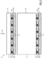
- the implementation shown in Fig. 1 can also be accomplished by means of two carrier layers 30a, 30b as shown in Fig. 2 depicting another embodiment of a photon counting detector 2.
- the photon counting detector 2 comprises a first carrier layer 30a arranged between the first direct conversion layer 10 and the second direct conversion layer 20 and a second carrier layer 30b arranged on a side of the second first direct conversion layer 20 facing away from the first direct conversion layer 10.
- the first terminals 31 are arranged on a surface side 38a of the first carrier layer 30a facing the first direct conversion layer 10 and being in contact with the first electrical contacts 12.
- the second terminals 32 are arranged on a surface side 39b of the second carrier layer 30b facing the second direct conversion layer 20 and being in contact with the second electrical contacts 22.
- the processing unit 35 is either arranged in the first carrier layer 30a or in the second carrier layer 30b, or in both layers 30a and 30b independently, or partly in both carrier layers 30a, 30b.
- Interconnection means e.g. one or more flex cables and/or integrated conductive lines
- connecting two processing units and/or connecting the pixels 36 with the processing unit(s) 35 may be provided (not shown in Fig. 2 ).
- a flex cable is taking the signals out from one carrier layer on one side and leading it to the other carrier layer on the same side or on the other side. A flex cable could thus be used to establish communication between both carrier layers if required.
- flex cables may be provided to lead the signals from both carrier layers to an external correction device (see Fig. 3 ).
- no processing unit may even be provided in any carrier layer, but the complete signal processing including the above described correction may be provided in the external correction device, either on the fly or when desired.
- Fig. 3 shows a schematic diagram of a correction device 40 according to the present invention.
- the correction device 40 substantially corresponds to the processing unit 35 and can be used as external means in combination with a photon counting detector as illustrated above, which does not have an internal processing unit 35.
- the correction device 40 may e.g. be implemented as a (programmed) processor or (programmed) computer or dedicated hardware.
- the correction device 40 comprises a first signal input 41 configured to obtain a first count signal representing high-energy electromagnetic radiation 100 impinging on the low-absorption direct conversion material 11 of the first direct conversion layer 10.
- the correction device 40 comprises a second signal input 42 configured to obtain a second count signal representing high-energy electromagnetic radiation 100 impinging on the high-absorption direct conversion material 21 of the second direct conversion layer 20.
- the first and second signal inputs 41, 42 may be implemented as a common signal input, e.g. in the form of a data or signal interface receiving the first and second count signals from the photo counting detector, in particular the pixels of the photon counting detector.
- the correction device further comprises processing circuitry 43 configured to correct, based on the first count signal, the second count signal for errors in one of the ways described above.
- the corrected second count signal alone or combined with the first count signal, which also provides information, may finally be used as the measurement signal of the photo counting detector, which is then further processed as desired by the application, e.g. which is used for generating an image of the scanned object.
- Another embodiment of the correction which may be applied by the correction device 40 or the processing unit 35, uses an iterative process to iteratively correct the measured data in the following way.
- a set of calibrations may be acquired in known conditions, particularly at low flux to minimize the artefacts of the bottom layer 20.
- This set of calibrations c is obtained with a number of materials m (leading to a plurality of baseline material decompositions).
- the measured data is used to perform an initial material decomposition A. Due to the materials used, it is known that the measurement G of the top layer 10 is correct and that the measurement C of the bottom layer 20 may be corrupted. G is probably a noisy measurement but with low bias (i.e., is quite accurate).
- the result of the material composition A is used to find the calibration data that correspond to the best fit (optionally the closest neighbor).
- the calibration data is use to scale the measurement C of the bottom layer 20. Based thereon a new material decomposition A' is calculated. This is likely an iterative process.
- Fig. 4 shows a schematic diagram of a photon counting detection arrangement 50. It comprises a photo counting detector as disclosed herein (in this embodiment as depicted in Fig. 1 ; alternatively (not shown) as depicted in Fig. 2 ), but without having any processing circuitry as part of the carrier layer(s) 30. Further, a correction device 40 as disclosed herein, e.g. as shown in Fig. 3 ) is provided, Connection means 51, such as a flex cable, connects the first and second terminals 31, 32 of the carrier layer 30 (directly or, as shown in Fig. 4 ) via the pixels 36 to the correction device 40. In this way, the proposed correction is done externally in the correction device 40.
- Connection means 51 such as a flex cable
- the present invention can preferably be applied for CT, such as spectral CT, but can generally be applied in all applications in which high-energy electromagnetic radiation shall be detected, particularly for imaging purposes, such as in medical imaging.
Landscapes
- Physics & Mathematics (AREA)
- Health & Medical Sciences (AREA)
- Life Sciences & Earth Sciences (AREA)
- General Physics & Mathematics (AREA)
- High Energy & Nuclear Physics (AREA)
- Molecular Biology (AREA)
- Spectroscopy & Molecular Physics (AREA)
- Measurement Of Radiation (AREA)
- Apparatus For Radiation Diagnosis (AREA)
Priority Applications (6)
| Application Number | Priority Date | Filing Date | Title |
|---|---|---|---|
| EP18186822.5A EP3605151A1 (fr) | 2018-08-01 | 2018-08-01 | Détecteur de comptage de photons |
| US17/263,916 US11448781B2 (en) | 2018-08-01 | 2019-08-01 | Photon counting detector |
| JP2021505256A JP7181378B2 (ja) | 2018-08-01 | 2019-08-01 | 光子カウントディテクター |
| CN201980051358.8A CN112543878B (zh) | 2018-08-01 | 2019-08-01 | 光子计数探测器 |
| PCT/EP2019/070753 WO2020025743A1 (fr) | 2018-08-01 | 2019-08-01 | Détecteur de comptage de photons |
| EP19745171.9A EP3830606A1 (fr) | 2018-08-01 | 2019-08-01 | Détecteur de comptage de photons |
Applications Claiming Priority (1)
| Application Number | Priority Date | Filing Date | Title |
|---|---|---|---|
| EP18186822.5A EP3605151A1 (fr) | 2018-08-01 | 2018-08-01 | Détecteur de comptage de photons |
Publications (1)
| Publication Number | Publication Date |
|---|---|
| EP3605151A1 true EP3605151A1 (fr) | 2020-02-05 |
Family
ID=63113446
Family Applications (2)
| Application Number | Title | Priority Date | Filing Date |
|---|---|---|---|
| EP18186822.5A Withdrawn EP3605151A1 (fr) | 2018-08-01 | 2018-08-01 | Détecteur de comptage de photons |
| EP19745171.9A Withdrawn EP3830606A1 (fr) | 2018-08-01 | 2019-08-01 | Détecteur de comptage de photons |
Family Applications After (1)
| Application Number | Title | Priority Date | Filing Date |
|---|---|---|---|
| EP19745171.9A Withdrawn EP3830606A1 (fr) | 2018-08-01 | 2019-08-01 | Détecteur de comptage de photons |
Country Status (5)
| Country | Link |
|---|---|
| US (1) | US11448781B2 (fr) |
| EP (2) | EP3605151A1 (fr) |
| JP (1) | JP7181378B2 (fr) |
| CN (1) | CN112543878B (fr) |
| WO (1) | WO2020025743A1 (fr) |
Families Citing this family (1)
| Publication number | Priority date | Publication date | Assignee | Title |
|---|---|---|---|---|
| GB202313150D0 (en) * | 2023-08-30 | 2023-10-11 | Res & Innovation Uk | Detection device |
Citations (5)
| Publication number | Priority date | Publication date | Assignee | Title |
|---|---|---|---|---|
| JPH02259590A (ja) * | 1989-03-31 | 1990-10-22 | Shimadzu Corp | 放射線検出装置 |
| US20080230709A1 (en) | 2007-03-23 | 2008-09-25 | Tkaczyk J Eric | Energy discriminating detector different materials direct conversion layers |
| DE102012215818A1 (de) * | 2012-09-06 | 2014-03-06 | Siemens Aktiengesellschaft | Strahlungsdetektor und Verfahren zur Herstellung eines Strahlungsdetektors |
| US20160206255A1 (en) * | 2015-01-16 | 2016-07-21 | Kabushiki Kaisha Toshiba | Hybrid passive/active multi-layer energy discriminating photon-counting detector |
| US9625589B2 (en) * | 2012-08-13 | 2017-04-18 | Koninklijke Philips N.V. | Photon counting x-ray detector |
Family Cites Families (11)
| Publication number | Priority date | Publication date | Assignee | Title |
|---|---|---|---|---|
| US7260174B2 (en) * | 2004-09-13 | 2007-08-21 | General Electric Company | Direct conversion energy discriminating CT detector with over-ranging correction |
| JP5697982B2 (ja) * | 2007-09-07 | 2015-04-08 | コーニンクレッカ フィリップス エヌ ヴェ | 複数の変換層を持つ放射線検出器、x線検出器および画像形成システム |
| US8729478B2 (en) | 2010-06-09 | 2014-05-20 | Carestream Health, Inc. | Dual screen radiographic detector with improved spatial sampling |
| EP2652525B1 (fr) | 2010-12-13 | 2016-09-21 | Koninklijke Philips N.V. | Détecteur de rayonnement doté de photodétecteurs |
| DE102011076781B4 (de) * | 2011-05-31 | 2018-05-03 | Siemens Healthcare Gmbh | Verfahren zur Korrektur einer Zählratendrift bei einem quantenzählenden Detektor, Röntgen-System mit quantenzählendem Detektor und Schaltungsanordnung für einen quantenzählenden Detektor |
| GB201120165D0 (en) * | 2011-11-23 | 2012-01-04 | Kromek Ltd | Detector apparatus and method |
| JP6310471B2 (ja) * | 2012-11-09 | 2018-04-11 | コーニンクレッカ フィリップス エヌ ヴェKoninklijke Philips N.V. | 検出器結晶のためのサブバンド赤外照射 |
| US9759822B2 (en) * | 2013-11-27 | 2017-09-12 | Koninklijke Philips N.V. | Detection device for detecting photons and method therefore |
| WO2016091981A1 (fr) * | 2014-12-11 | 2016-06-16 | Koninklijke Philips N.V. | Détecteur de rayons x, appareil d'imagerie et procédé d'étalonnage |
| US10646176B2 (en) * | 2015-09-30 | 2020-05-12 | General Electric Company | Layered radiation detector |
| WO2017116392A1 (fr) * | 2015-12-28 | 2017-07-06 | Analogic Corporation | Réseau de détecteurs pour modalité d'imagerie par rayonnement |
-
2018
- 2018-08-01 EP EP18186822.5A patent/EP3605151A1/fr not_active Withdrawn
-
2019
- 2019-08-01 CN CN201980051358.8A patent/CN112543878B/zh active Active
- 2019-08-01 US US17/263,916 patent/US11448781B2/en active Active
- 2019-08-01 EP EP19745171.9A patent/EP3830606A1/fr not_active Withdrawn
- 2019-08-01 WO PCT/EP2019/070753 patent/WO2020025743A1/fr not_active Ceased
- 2019-08-01 JP JP2021505256A patent/JP7181378B2/ja active Active
Patent Citations (5)
| Publication number | Priority date | Publication date | Assignee | Title |
|---|---|---|---|---|
| JPH02259590A (ja) * | 1989-03-31 | 1990-10-22 | Shimadzu Corp | 放射線検出装置 |
| US20080230709A1 (en) | 2007-03-23 | 2008-09-25 | Tkaczyk J Eric | Energy discriminating detector different materials direct conversion layers |
| US9625589B2 (en) * | 2012-08-13 | 2017-04-18 | Koninklijke Philips N.V. | Photon counting x-ray detector |
| DE102012215818A1 (de) * | 2012-09-06 | 2014-03-06 | Siemens Aktiengesellschaft | Strahlungsdetektor und Verfahren zur Herstellung eines Strahlungsdetektors |
| US20160206255A1 (en) * | 2015-01-16 | 2016-07-21 | Kabushiki Kaisha Toshiba | Hybrid passive/active multi-layer energy discriminating photon-counting detector |
Also Published As
| Publication number | Publication date |
|---|---|
| WO2020025743A1 (fr) | 2020-02-06 |
| JP7181378B2 (ja) | 2022-11-30 |
| CN112543878B (zh) | 2024-07-26 |
| US20210302599A1 (en) | 2021-09-30 |
| US11448781B2 (en) | 2022-09-20 |
| EP3830606A1 (fr) | 2021-06-09 |
| CN112543878A (zh) | 2021-03-23 |
| JP2021533347A (ja) | 2021-12-02 |
Similar Documents
| Publication | Publication Date | Title |
|---|---|---|
| US7696483B2 (en) | High DQE photon counting detector using statistical recovery of pile-up events | |
| US7613274B2 (en) | Method and system of energy integrating and photon counting using layered photon counting detector | |
| EP2929372B1 (fr) | Procédé et appareil pour la correction d'image d'informations d'image de rayons x | |
| KR101999266B1 (ko) | 엑스선 영상 장치 및 그 제어 방법 | |
| EP2883083B1 (fr) | Détecteur de rayons x à comptage de photons | |
| CN108918559B (zh) | 一种实现图像自校正的x射线图像探测器及其方法 | |
| US20160334521A1 (en) | Method for Calibrating a Counting Digital X-Ray Detector, X-Ray System for Performing Such a Method and Method for Acquiring an X-Ray Image | |
| US20100213381A1 (en) | Radiation detector with several conversion layers | |
| US20120085915A1 (en) | Processing electronics and method for determining a count result, and detector for an x-ray imaging device | |
| US11435488B2 (en) | Photon counting spectral CT | |
| EP1423733B1 (fr) | Procede et dispositif d'identification et de correction d'artefacts de ligne dans un detecteur de rayons x a solide | |
| US7573025B2 (en) | Energy calibration method and radiation detecting and radiological imaging apparatus | |
| US8927939B2 (en) | Radiation measurement apparatus and nuclear medicine diagnosis apparatus | |
| EP3508887A1 (fr) | Procédé et système d'étalonnage et de partage de charge | |
| US10627532B2 (en) | Dead-time calibration for a radiation detector | |
| CN105093255B (zh) | 射线探测方法、装置、探测器组件和射线探测器 | |
| US11448781B2 (en) | Photon counting detector | |
| JP2002034961A (ja) | 放射線撮影装置及び放射線撮影方法 | |
| JP2007510150A (ja) | ピクセル状固体検出器のための較正方法および装置 | |
| EP1935340B1 (fr) | Procédé pour neutraliser des artefacts d'image avant la détermination du rapport du signal pour le bruit dans des systèmes de radiographie CR/DR |
Legal Events
| Date | Code | Title | Description |
|---|---|---|---|
| PUAI | Public reference made under article 153(3) epc to a published international application that has entered the european phase |
Free format text: ORIGINAL CODE: 0009012 |
|
| AK | Designated contracting states |
Kind code of ref document: A1 Designated state(s): AL AT BE BG CH CY CZ DE DK EE ES FI FR GB GR HR HU IE IS IT LI LT LU LV MC MK MT NL NO PL PT RO RS SE SI SK SM TR |
|
| AX | Request for extension of the european patent |
Extension state: BA ME |
|
| RAP1 | Party data changed (applicant data changed or rights of an application transferred) |
Owner name: KONINKLIJKE PHILIPS N.V. |
|
| STAA | Information on the status of an ep patent application or granted ep patent |
Free format text: STATUS: THE APPLICATION IS DEEMED TO BE WITHDRAWN |
|
| 18D | Application deemed to be withdrawn |
Effective date: 20200806 |