EP3605564B1 - Komponententräger mit eingebettetem induktor mit einer einlage - Google Patents
Komponententräger mit eingebettetem induktor mit einer einlage Download PDFInfo
- Publication number
- EP3605564B1 EP3605564B1 EP19188903.9A EP19188903A EP3605564B1 EP 3605564 B1 EP3605564 B1 EP 3605564B1 EP 19188903 A EP19188903 A EP 19188903A EP 3605564 B1 EP3605564 B1 EP 3605564B1
- Authority
- EP
- European Patent Office
- Prior art keywords
- magnetic
- component carrier
- component
- inductor
- stack
- Prior art date
- Legal status (The legal status is an assumption and is not a legal conclusion. Google has not performed a legal analysis and makes no representation as to the accuracy of the status listed.)
- Active
Links
Images

Classifications
-
- H—ELECTRICITY
- H01—ELECTRIC ELEMENTS
- H01F—MAGNETS; INDUCTANCES; TRANSFORMERS; SELECTION OF MATERIALS FOR THEIR MAGNETIC PROPERTIES
- H01F27/00—Details of transformers or inductances, in general
- H01F27/02—Casings
- H01F27/022—Encapsulation
-
- H—ELECTRICITY
- H01—ELECTRIC ELEMENTS
- H01F—MAGNETS; INDUCTANCES; TRANSFORMERS; SELECTION OF MATERIALS FOR THEIR MAGNETIC PROPERTIES
- H01F17/00—Fixed inductances of the signal type
- H01F17/0006—Printed inductances
- H01F17/0013—Printed inductances with stacked layers
-
- H—ELECTRICITY
- H01—ELECTRIC ELEMENTS
- H01F—MAGNETS; INDUCTANCES; TRANSFORMERS; SELECTION OF MATERIALS FOR THEIR MAGNETIC PROPERTIES
- H01F17/00—Fixed inductances of the signal type
- H01F17/0006—Printed inductances
- H01F17/0033—Printed inductances with the coil helically wound around a magnetic core
-
- H—ELECTRICITY
- H01—ELECTRIC ELEMENTS
- H01F—MAGNETS; INDUCTANCES; TRANSFORMERS; SELECTION OF MATERIALS FOR THEIR MAGNETIC PROPERTIES
- H01F27/00—Details of transformers or inductances, in general
- H01F27/24—Magnetic cores
-
- H—ELECTRICITY
- H01—ELECTRIC ELEMENTS
- H01F—MAGNETS; INDUCTANCES; TRANSFORMERS; SELECTION OF MATERIALS FOR THEIR MAGNETIC PROPERTIES
- H01F27/00—Details of transformers or inductances, in general
- H01F27/28—Coils; Windings; Conductive connections
- H01F27/2804—Printed windings
-
- H—ELECTRICITY
- H01—ELECTRIC ELEMENTS
- H01F—MAGNETS; INDUCTANCES; TRANSFORMERS; SELECTION OF MATERIALS FOR THEIR MAGNETIC PROPERTIES
- H01F41/00—Apparatus or processes specially adapted for manufacturing or assembling magnets, inductances or transformers; Apparatus or processes specially adapted for manufacturing materials characterised by their magnetic properties
- H01F41/02—Apparatus or processes specially adapted for manufacturing or assembling magnets, inductances or transformers; Apparatus or processes specially adapted for manufacturing materials characterised by their magnetic properties for manufacturing cores, coils, or magnets
- H01F41/0206—Manufacturing of magnetic cores by mechanical means
-
- H—ELECTRICITY
- H01—ELECTRIC ELEMENTS
- H01F—MAGNETS; INDUCTANCES; TRANSFORMERS; SELECTION OF MATERIALS FOR THEIR MAGNETIC PROPERTIES
- H01F41/00—Apparatus or processes specially adapted for manufacturing or assembling magnets, inductances or transformers; Apparatus or processes specially adapted for manufacturing materials characterised by their magnetic properties
- H01F41/02—Apparatus or processes specially adapted for manufacturing or assembling magnets, inductances or transformers; Apparatus or processes specially adapted for manufacturing materials characterised by their magnetic properties for manufacturing cores, coils, or magnets
- H01F41/04—Apparatus or processes specially adapted for manufacturing or assembling magnets, inductances or transformers; Apparatus or processes specially adapted for manufacturing materials characterised by their magnetic properties for manufacturing cores, coils, or magnets for manufacturing coils
- H01F41/041—Printed circuit coils
-
- H—ELECTRICITY
- H01—ELECTRIC ELEMENTS
- H01F—MAGNETS; INDUCTANCES; TRANSFORMERS; SELECTION OF MATERIALS FOR THEIR MAGNETIC PROPERTIES
- H01F41/00—Apparatus or processes specially adapted for manufacturing or assembling magnets, inductances or transformers; Apparatus or processes specially adapted for manufacturing materials characterised by their magnetic properties
- H01F41/02—Apparatus or processes specially adapted for manufacturing or assembling magnets, inductances or transformers; Apparatus or processes specially adapted for manufacturing materials characterised by their magnetic properties for manufacturing cores, coils, or magnets
- H01F41/04—Apparatus or processes specially adapted for manufacturing or assembling magnets, inductances or transformers; Apparatus or processes specially adapted for manufacturing materials characterised by their magnetic properties for manufacturing cores, coils, or magnets for manufacturing coils
- H01F41/041—Printed circuit coils
- H01F41/046—Printed circuit coils structurally combined with ferromagnetic material
-
- H—ELECTRICITY
- H02—GENERATION; CONVERSION OR DISTRIBUTION OF ELECTRIC POWER
- H02M—APPARATUS FOR CONVERSION BETWEEN AC AND AC, BETWEEN AC AND DC, OR BETWEEN DC AND DC, AND FOR USE WITH MAINS OR SIMILAR POWER SUPPLY SYSTEMS; CONVERSION OF DC OR AC INPUT POWER INTO SURGE OUTPUT POWER; CONTROL OR REGULATION THEREOF
- H02M1/00—Details of apparatus for conversion
-
- H—ELECTRICITY
- H02—GENERATION; CONVERSION OR DISTRIBUTION OF ELECTRIC POWER
- H02M—APPARATUS FOR CONVERSION BETWEEN AC AND AC, BETWEEN AC AND DC, OR BETWEEN DC AND DC, AND FOR USE WITH MAINS OR SIMILAR POWER SUPPLY SYSTEMS; CONVERSION OF DC OR AC INPUT POWER INTO SURGE OUTPUT POWER; CONTROL OR REGULATION THEREOF
- H02M7/00—Conversion of AC power input into DC power output; Conversion of DC power input into AC power output
- H02M7/003—Constructional details, e.g. physical layout, assembly, wiring or busbar connections
-
- H—ELECTRICITY
- H05—ELECTRIC TECHNIQUES NOT OTHERWISE PROVIDED FOR
- H05K—PRINTED CIRCUITS; CASINGS OR CONSTRUCTIONAL DETAILS OF ELECTRIC APPARATUS; MANUFACTURE OF ASSEMBLAGES OF ELECTRICAL COMPONENTS
- H05K1/00—Printed circuits
- H05K1/16—Printed circuits incorporating printed electric components, e.g. printed resistors, capacitors or inductors
- H05K1/165—Printed circuits incorporating printed electric components, e.g. printed resistors, capacitors or inductors incorporating printed inductors
-
- H—ELECTRICITY
- H05—ELECTRIC TECHNIQUES NOT OTHERWISE PROVIDED FOR
- H05K—PRINTED CIRCUITS; CASINGS OR CONSTRUCTIONAL DETAILS OF ELECTRIC APPARATUS; MANUFACTURE OF ASSEMBLAGES OF ELECTRICAL COMPONENTS
- H05K1/00—Printed circuits
- H05K1/18—Printed circuits structurally associated with non-printed electric components
- H05K1/182—Printed circuits structurally associated with non-printed electric components associated with components mounted in printed circuit boards [PCB], e.g. insert-mounted components [IMC]
- H05K1/185—Printed circuits structurally associated with non-printed electric components associated with components mounted in printed circuit boards [PCB], e.g. insert-mounted components [IMC] associated with components encapsulated in the insulating substrate of the PCBs; associated with components incorporated in internal layers of multilayer circuit boards
-
- H—ELECTRICITY
- H01—ELECTRIC ELEMENTS
- H01F—MAGNETS; INDUCTANCES; TRANSFORMERS; SELECTION OF MATERIALS FOR THEIR MAGNETIC PROPERTIES
- H01F17/00—Fixed inductances of the signal type
- H01F17/0006—Printed inductances
- H01F2017/0066—Printed inductances with a magnetic layer
-
- H—ELECTRICITY
- H01—ELECTRIC ELEMENTS
- H01F—MAGNETS; INDUCTANCES; TRANSFORMERS; SELECTION OF MATERIALS FOR THEIR MAGNETIC PROPERTIES
- H01F27/00—Details of transformers or inductances, in general
- H01F27/28—Coils; Windings; Conductive connections
- H01F27/2804—Printed windings
- H01F2027/2809—Printed windings on stacked layers
Definitions
- the invention relates to a method of manufacturing a component carrier, to a component carrier, and to an electric device with the component carrier.
- component carriers equipped with one or more electronic components and increasing miniaturization of such components as well as a rising number of components to be connected to the component carriers such as printed circuit boards, increasingly more powerful array-like components or packages having several components are being employed, which have a plurality of contacts or connections, with ever smaller spacing between these contacts.
- component carriers shall be mechanically robust and electrically reliable so as to be operable even under harsh conditions.
- a component carrier as defined in present claim 1 and a method of manufacturing a component carrier as defined in present claim 11 are provided.
- Preferred embodiments are defined in the dependent claims.
- component carrier may particularly denote any support structure which is capable of accommodating one or more components thereon and/or therein for providing mechanical support and/or electrical connectivity.
- a component carrier may be configured as a mechanical and/or electronic carrier for components.
- a component carrier may be one of a printed circuit board, an organic interposer, and an IC (integrated circuit) substrate.
- a component carrier may also be a hybrid board combining different ones of the above mentioned types of component carriers.
- the term "inductor” may particularly denote a passive (in particular two-terminal, for instance inductance, or four-terminal, for instance transformer) electrical component that is capable of storing energy in a magnetic field when electric current flows through the inductor.
- An inductor may comprise an electrically conductive wiring wound into a coil shape around a magnetic core.
- wind structure may particularly denote an at least partially electrically conductive structure, which may be composed of one or multiple connected electrically conductive elements, defining one or multiple windings.
- the windings may have a circular shape, a rectangular shape, any other polygonal shape, etc.
- coil opening may particularly denote a through hole extending through an interior of one or more windings of the coil structure.
- magnetic core may particularly denote a body of magnetic material, which body may be composed of one or multiple connected or spaced magnetic elements.
- the magnetic core may increase the magnetic field and thus the inductance of the inductor.
- such a magnetic core may comprise or consist of iron and/or ferrite.
- the term "inlay” may particularly denote a pre-manufactured member which can be inserted into a cavity of the stack of layer structures as a whole.
- the inlay can be manufactured in accordance with the requirements of its function, independently of boundary conditions of component carrier manufacturing technology.
- such one or more inlays may be inserted in any free region of the component carrier, as far as within the scope of present claim 1, so that a component carrier designer has a high flexibility and freedom of designing the embedded inductor.
- relatively high inductance values may be achieved by the described manufacturing technology.
- this manufacturing architecture allows for a high integration density, in particular for applications such as power electronic converters (for instance DC/DC converters, DC/AC converters). Beyond this, the manufacturing process is also compatible with the formation of coupled inductors, i.e. multiple inductors in functional relationship within a common component carrier.
- the described component carrier with embedded inductor as a component which can be mounted on or in a support body such as another component carrier.
- the finished component carrier with embedded inductor can be used itself as surface mounted device (SMD) or as an embedded component.
- the coil structure is partially or completely configured as inlay, while the magnetic core forms part of the laminated stack.
- the coil structure forms part of the laminated stack, while the magnetic core is partially or completely configured as inlay.
- both coil structure and magnetic core are partially or completely configured as inlay.
- At least part of at least one of the coil structure and the magnetic core forms part of the laminated stack rather than being configured as an inlay embedded in the stack.
- one of the coil structure and the magnetic core may be a separate inlay, it may be also advantageous that another one of the core structure and the magnetic core forms part of the stack of layer structures of the component carrier.
- the latter can then be synergistically used also as a constituent of the embedded inductor.
- patterned copper foils in combination with vertical through connections made of copper (for example copper filled laser vias) between and/or in resin layers (optionally comprising glass fibers) of the component carrier stack may be combined so as to form one or more windings in component carrier material.
- Portions of the component carrier stack which are not used for other tasks may thus be functionalized to form part of the embedded inductor.
- a hybrid inductor embedded in a component carrier may be provided, wherein part of the hybrid inductor is formed by a specifically configurable inlay, and another part of the hybrid inductor may be formed by component carrier material (in particular a layer stack thereof).
- component carrier material in particular a layer stack thereof.
- the coil structure comprises interconnected electrically conductive elements surrounded by a dielectric matrix.
- the electrically conductive elements may be made of copper (for instance in an embodiment in which the inductor is embedded in a PCB board) or aluminum (for instance in an embodiment in which the inductor is embedded in an IMS board).
- the dielectric matrix may for instance be prepreg or FR4.
- the magnetic core comprises a plurality of separate magnetic bodies.
- Such magnetic bodies may be in particular one or more magnetic sheets, one or more magnetic posts, and/or one or more magnetic paste structures.
- the embedded inductor may be formed by stacking multiple magnetic bodies, in particular two or three layers of magnetic bodies. Additionally or alternatively, it is also possible to arrange multiple magnetic bodies in the same layer.
- magnetic posts may be cut (for instance by laser cutting) based on magnetic sheets.
- Magnetic paste may for instance be applied by screen printing, in particular to close magnetic paths by filling remaining air gaps.
- a surface of at least part of the magnetic core has a roughness Ra of less than 4 ⁇ m, in particular less than 2 ⁇ m.
- the value of the roughness Ra may be preferably less than 500 nm.
- the roughness of a surface may be defined as and may be measured as the centerline average height Ra. Ra is the arithmetic mean value of all distances of the profile from the centerline. For instance, the measurement may be carried out according to DIN 4768.
- the mentioned low roughness values as a result of precisely defined cutting surfaces can be obtained by forming at least one magnetic element of the magnetic core by laser cutting of a magnetic body. With such smooth and precisely defined cutting surfaces, the magnetic properties of the magnetic core may be adjusted with high accuracy.
- magnetic bodies formed by laser processing of ferrite bodies suffer much less from such shortcomings.
- At least a part of the magnetic cores of the inductor and the at least one further inductor are formed as an integral structure, in particular is a common magnetic sheet.
- Such a configuration is simple to manufacture, involves only low magnetic losses and allows for a compact design (compare for instance Figure 5 ).
- the magnetic core comprises a magnetic post extending through the coil opening and comprises a magnetic sheet extending laterally beyond the magnetic post and at least partially over the coil structure.
- the magnetic core comprises a further magnetic sheet extending laterally beyond the magnetic post and at least partially over the coil structure, wherein the magnetic post is arranged between the magnetic sheet and the further magnetic sheet.
- the magnetic core comprises at least one further magnetic post extending parallel to the magnetic post, wherein the coil structure is arranged between the magnetic post and the at least one further magnetic post.
- a circumferentially closed magnetic core may be obtained (compare for instance Figure 1 ).
- the component carrier comprises at least one component embedded in the component carrier.
- a component may be an active component or a passive component.
- Components capable of controlling current by means of another electrical signal may be denoted as active components (for instance semiconductor chips).
- active components for instance semiconductor chips
- passive devices Components incapable of controlling current by means of another electrical signal.
- Resistors or capacitors are examples for passive components.
- the at least one component may be embedded in one of the group consisting of the stack, the coil structure, and the magnetic core.
- the at least one component may comprise a resistor. It is also possible that the at least one component comprises an adjustable resistor or a transistor (i.e. in particular a transfer resistor).
- the at least one component may be located directly next to the coil structure, in particular in direct physical contact with the coil structure. In other words, the embedded components may be positioned directly adjacent to the coil structure or windings thereof. For example, the at least one component may be embedded between windings of the coil structure of the inductor.
- the at least one component can be selected from a group consisting of an electrically non-conductive inlay, an electrically conductive inlay (such as a metal inlay, preferably comprising copper or aluminum), a heat transfer unit (for example a heat pipe), a light guiding element (for example an optical waveguide or a light conductor connection), an electronic component, or combinations thereof.
- an electrically non-conductive inlay such as a metal inlay, preferably comprising copper or aluminum
- a heat transfer unit for example a heat pipe
- a light guiding element for example an optical waveguide or a light conductor connection
- an electronic component or combinations thereof.
- the component can be an active electronic component, a passive electronic component, an electronic chip, a storage device (for instance a DRAM or another data memory), a filter, an integrated circuit, a signal processing component, a power management component, an optoelectronic interface element, a voltage converter (for example a DC/DC converter or an AC/DC converter), a cryptographic component, a transmitter and/or receiver, an electromechanical transducer, a sensor, an actuator, a microelectromechanical system (MEMS), a microprocessor, a capacitor, a resistor, an inductance, a battery, a switch, a camera, an antenna, a logic chip, and an energy harvesting unit.
- other components may be embedded in the component carrier.
- a magnetic element can be used as a component.
- a magnetic element may be a permanent magnetic element (such as a ferromagnetic element, an antiferromagnetic element or a ferrimagnetic element, for instance a ferrite core) or may be a paramagnetic element.
- the component may also be a further component carrier (for example a printed circuit board, a substrate, or an interposer) in a board-in-board configuration.
- the component may be surface mounted on the component carrier and/or may be embedded in an interior thereof.
- other components in particular those which generate and emit electromagnetic radiation and/or are sensitive with regard to electromagnetic radiation propagating from an environment, may be used as component.
- the component carrier comprises a stack of at least one electrically insulating layer structure and at least one electrically conductive layer structure.
- the component carrier may be a laminate of the mentioned electrically insulating layer structure(s) and electrically conductive layer structure(s), in particular formed by applying mechanical pressure, if desired supported by thermal energy.
- the mentioned stack may provide a plate-shaped component carrier capable of providing a large mounting surface for further components and being nevertheless very thin and compact.
- layer structure may particularly denote a continuous layer, a patterned layer or a plurality of non-consecutive islands within a common plane.
- the component carrier is shaped as a plate. This contributes to the compact design, wherein the component carrier nevertheless provides a large basis for mounting components thereon. Furthermore, in particular a naked die as example for an embedded electronic component, can be conveniently embedded, thanks to its small thickness, into a thin plate such as a printed circuit board.
- the component carrier is configured as one of the group consisting of a printed circuit board, and a substrate (in particular an IC substrate).
- PCB printed circuit board
- a component carrier which may be plate-shaped (i.e. planar), three-dimensionally curved (for instance when manufactured using 3D printing) or which may have any other shape) which is formed by laminating several electrically conductive layer structures with several electrically insulating layer structures, for instance by applying pressure, if desired accompanied by the supply of thermal energy.
- the electrically conductive layer structures are made of copper
- the electrically insulating layer structures may comprise resin and/or glass fibers, so-called prepreg or FR4 material.
- the various electrically conductive layer structures may be connected to one another in a desired way by forming through-holes through the laminate, for instance by laser drilling or mechanical drilling, and by filling them with electrically conductive material (in particular copper), thereby forming vias as through-hole connections.
- electrically conductive material in particular copper
- a printed circuit board is usually configured for accommodating one or more components on one or both opposing surfaces of the plate-shaped printed circuit board. They may be connected to the respective main surface by soldering.
- a dielectric part of a PCB may be composed of resin with reinforcing fibers (such as glass fibers).
- the term "substrate” may particularly denote a small component carrier having substantially the same size as a component (in particular an electronic component) to be mounted thereon. More specifically, a substrate can be understood as a carrier for electrical connections or electrical networks as well as component carrier comparable to a printed circuit board (PCB), however with a considerably higher density of laterally and/or vertically arranged connections. Lateral connections are for example conductive paths, whereas vertical connections may be for example drill holes. These lateral and/or vertical connections are arranged within the substrate and can be used to provide electrical and/or mechanical connections of housed components or unhoused components (such as bare dies), particularly of IC chips, with a printed circuit board or intermediate printed circuit board. Thus, the term “substrate” also includes "IC substrates". A dielectric part of a substrate may be composed of resin with reinforcing spheres (such as glass spheres).
- a substrate or interposer may comprises or consist of at least a layer of glass, silicon, ceramic and/or organic material (like resin).
- a substrate or interposer may also comprises a photoimageable or dry-etchable organic material like epoxy-based Build-Up films or polymer compounds like Polyimide, Polybenzoxazole, or Benzocyclobutene.
- the at least one electrically insulating layer structure comprises at least one of the group consisting of resin (such as reinforced or non-reinforced resins, for instance epoxy resin or Bismaleimide-Triazine resin, more specifically FR-4 or FR-5), cyanate ester, polyphenylene derivate, glass (in particular glass fibers, glass-spheres, multi-layer glass, glass-like materials), prepreg material, photoimageable dielectric material, polyimide, polyamide, liquid crystal polymer (LCP), epoxy-based Build-Up Film, polytetrafluoroethylene (Teflon), a ceramic, and a metal oxide.
- resin such as reinforced or non-reinforced resins, for instance epoxy resin or Bismaleimide-Triazine resin, more specifically FR-4 or FR-5
- cyanate ester such as reinforced or non-reinforced resins, for instance epoxy resin or Bismaleimide-Triazine resin, more specifically FR-4 or FR-5
- polyphenylene derivate
- Reinforcing materials such as webs, fibers or spheres, for example made of glass (multilayer glass) may be used as well. Although prepreg, FR4, or epoxy-based Build-Up Film or photoimageable dielectrics are usually preferred, other materials may be used as well. For high frequency applications, high-frequency materials such as polytetrafluoroethylene, liquid crystal polymer and/or cyanate ester resins may be implemented in the component carrier as electrically insulating layer structure.
- the at least one electrically conductive layer structure comprises at least one of the group consisting of copper, aluminum, nickel, silver, gold, palladium, and tungsten.
- copper is usually preferred, other materials or coated versions thereof are possible as well, in particular coated with supra-conductive material such as graphene.
- the component carrier is a laminate-type component carrier.
- the component carrier is a compound of multiple layer structures which are stacked and connected together by applying a pressing force, if desired accompanied by heat.
- a component carrier with an embedded inductor with ultra-flexible structure is provided.
- Such an embedded inductor may be manufactured advantageously with a high degree of freedom.
- Magnetic material for example ferrite beads
- inductor may be used in combination with copper windings to form chokes, also called inductor.
- Such an inductor may be designed to have high inductance values at comparably small physical size.
- a component carrier in particular a PCB
- an inductor having substantially any desired shape.
- an inductor may comprise a coil structure (which may be formed as a number of connected copper windings), and a magnetic core with one or more pre-formed ferrite parts and optionally ferrite paste.
- the ferrite structure may be any appropriate magnetic structure capable of increasing the inductivity of the embedded inductor.
- One or more non-magnetic regions interrupting a closed loop magnetic path along magnetic material, for instance air gaps or electrically insulating regions of the component carrier, may be formed as part of the embedded inductor at any desired position at which they are needed for a specific application.
- An exemplary embodiment of the invention therefore provides an embedding process using multi-part magnetic cores being freely definable in accordance with a desired application.
- a component carrier with one or more embedded inlays may be provided fulfilling an inductor function.
- inductor with appropriate values of the inductivity for certain applications, for instance to operate it with high currents up to 30 A or more.
- a basic target of such applications may be to construct an inductor with small physical dimensions and high inductance values.
- inductive core materials can be used to generate any desired geometric shape. Around such a core a copper winding may be introduced to form the inductor. This leads to the advantage of a high degree of freedom during inductor construction combined with pronounced integration methods to form small power supply circuits.
- a PCB or another component carrier can be used to construct an inductor in substantially any desired shape.
- base materials for example prepreg.
- every combination of embedding and a build-up involving cavities (which may be formed for example using release layers having a poor adhesion with regard to surrounding component carrier material) is possible to be used for such embodiments.
- a non-magnetic region such as an air gap is introduced into the magnetic core of the embedded inductor to fine-tune the magnetic properties of the component carrier with the embedded inductor.
- a minimum air gap is 75 ⁇ m.
- a ferrite paste material can be printed before a press cycle.
- a pre-manufactured PCB inlay may be advantageously used.
- a coil structure may be embodied as a PCB (in particular with only two layers).
- the core structure is embodied as IC (integrated circuit) substrate, enabling a higher layer count.
- the mentioned inlay may be used in a board-in-board configuration.
- a component such as a die can also be embedded into the inlay inside the ferrite inductor. This may enable smallest package sizes which are only limited by the desired inductance value.
- the embedded inductor in the component carrier can have nearly any shape, as far as within the scope of present claim 1, so that the freedom of designing the shape for a component carrier designer is high. Furthermore, high inductance values are possible with the described manufacturing procedure. Furthermore, a high integration density may be obtained, which may be for instance advantageous for applications such as power electronic converters.
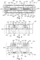
- Figure 1 illustrates a cross-sectional view of a plate-shaped laminate-type component carrier 100 with an embedded inductor 108 having a closed magnetic core 114 according to an exemplary embodiment not forming part of the invention.
- the component carrier 100 is here embodied as a printed circuit board (PCB).
- the component carrier 100 comprises a laminated stack 102 composed of electrically conductive layer structures 104 and electrically insulating layer structures 106.
- the electrically conductive layer structures 104 may comprise patterned copper foils and vertical through connections, for example copper filled laser vias.
- the electrically insulating layer structures 106 may comprise a resin (such as epoxy resin), optionally comprising reinforcing particles therein (for instance glass fibers or glass spheres).
- the electrically insulating layer structures 106 may be made of prepreg or FR4.
- the layer structures 104, 106 may be connected by lamination, i.e. the application of pressure and/or heat.
- the inductor 108 is embedded in the stack 102.
- one or more cavities may be formed in the stack 102, and a respective constituent of the inductor 108 may be inserted in such a cavity.
- a cavity may be formed by mechanically processing the stack 102, for instance by milling or drilling by mechanically processing or laser processing. It is also possible to form such a cavity by laminating a release layer in an interior of the stack 102.
- a release layer may be made of a material (for instance a waxy material, or polytetrafluoroethylene) having poor adhesion properties with regard to surrounding component carrier material.
- a piece of material of the stack 102 may then be cut out above the release layer, for instance by carrying out a circumferential cut using a laser or a mechanical drilling tool. The piece may then simply be taken out of the stack 102 due to the poor adhesion between the release layer and adjacent material of the stack 102, so that a cavity is obtained.
- the embedded inductor 108 comprises in particular two constituents, i.e. a coil structure 110 and the magnetic core 114.
- the electrically conductive coil structure 110 is wound with one or more windings around a central coil opening 112.
- a part of the magnetic core 114 fills the coil opening 112, whereas another part of the magnetic core 114 surrounds the coil structure 110 both laterally and vertically.
- the coil structure 110 comprises interconnected electrically conductive elements 116 surrounded by a dielectric matrix 118.
- the dielectric matrix 118 may electrically isolate electrically conductive elements 116 from one another and may contribute therefore to the formation of the one or more windings of the coil structure 110.
- the dielectric matrix 118 may be made for instance from resin (such as epoxy resin), and may optionally comprise reinforcing particles (such as glass fibers or glass spheres). In one embodiment, the dielectric matrix 118 may form part of the electrically insulating layer structures 106 of the stack 102.
- the electrically conductive elements 116 may be made of copper so as to be properly compatible with component carrier (in particular PCB) manufacturing technology. More specifically, the electrically conductive elements 116 comprise planar elements 120 extending within a horizontal plane. The planar elements 120 may be formed by patterning copper layers. As can be taken from Figure 1 , the planar elements 120 extend in parallel planes (wherein each of these planes corresponds to an assigned winding of the coil structure 110) which are also parallel to planes of the stacked electrically insulating layer structures 106 of the stack 102. The planar elements 120 may be connected with one another so as to form one or more windings of the coil structure 110.
- the planar elements 120 may even form part of the layer-type electrically conductive layer structures 104, i.e. can be embodied as correspondingly manufactured portions of the stack 102.
- the electrically conductive elements 116 additionally comprise vertical elements 122, for example copper filled laser vias.
- Each of the vertical elements 122 may mechanically and electrically connect planar elements 120 of adjacent layers.
- the planar elements 120 may in particular extend perpendicular to the planes of the planar elements 120.
- the vertical elements 122 may electrically and mechanically connect adjacent windings in different (in particular parallel) planes to thereby complete the formation of the coil structure 110.
- the vertical elements 122 may even form part of the electrically conductive layer structures 104 which are embodied as vertical through connections, i.e. can be embodied as correspondingly manufactured portions of the stack 102.
- the coil structure 110 forms part of the component carrier material. In such an embodiment, it is possible to manufacture the coil structure 110 in a region of the stack 102 which is not needed for the wiring functionality of component carrier 100.
- the coil structure 110 with their planar elements 120 and their vertical elements 122 can be embodied as an inlay, i.e. as a pre-manufactured component to be embedded in the stack 102.
- the coil structure 110 may then also be a small component carrier (such as a PCB or an IC substrate) which is embedded in the stack 102 in a board-in-board configuration.
- the coil structure 110 may have a ring shape being exteriorly delimited by the one or more windings formed by the electrically conductive elements 116 and having an interior through hole as coil opening 112.
- a ring may have a circular ring shape or a rectangular ring shape.
- the magnetic bodies forming the magnetic core 114 comprise two magnetic sheets 124 in two parallel planes, three magnetic posts 126 all arranged in a third plane between the two planes of the magnetic sheets 124, and six sections of magnetic paste 128 closing gaps between adjacent ones of the magnetic bodies in the three mentioned planes. Due to the shown configuration of the magnetic bodies, and in particular due to the magnetic paste 128 bridging magnetic sheets 124 and magnetic posts 126, the various magnetic bodies are magnetically connected to one another so as to form a closed magnetic ring path without non-magnetic gaps (such as air gaps) in between. By taking this measure, it can be ensured that the magnetic field remains substantially completely in an interior of the magnetic core 114 with low magnetic loss.
- the magnetic core 114 of Figure 1 comprises a central magnetic post 126 extending in a central plane through the coil opening 112.
- a bottom magnetic sheet 124 extends laterally beyond the magnetic post 126 and also extends laterally beyond the coil structure 110.
- the magnetic core 114 of Figure 1 comprises a top magnetic sheet 124 extending in a plane above the central magnetic post 126 and laterally beyond the magnetic post 126 and laterally beyond the coil structure 110.
- the central magnetic post 126 is arranged between the bottom magnetic sheet 124 and the top magnetic sheet 124.
- the magnetic core 114 comprises two further lateral magnetic posts 126 extending parallel to the central magnetic post 126 and laterally enclosing the central magnetic post 126. All three magnetic posts 126 are arranged coplanar, i.e. in a common plane.
- the coil structure 110 is arranged in a lateral or horizontal direction between the central magnetic post 126 and the two lateral magnetic posts 126.
- the magnetic posts 126 of the magnetic core 114 may be cut out from a larger magnetic body (such as a magnetic sheet 124) by laser cutting.
- a larger magnetic body such as a magnetic sheet 1214
- the surface properties of the magnetic posts 126 may be well defined and may be cut without a significant increase of the loss factor and without a significant decrease of magnetic permeability (as it may occur with conventional grinding procedures), substantially without surface profile and with low surface roughness.
- the magnetic properties of the embedded inductor 108 may therefore be adjusted accurately.
- the cut surfaces of the magnetic posts 126 may have a roughness Ra of preferably less than 500 nm.
- the magnetic posts 126 may be treated as embedded components or inlays, i.e. may be embedded in cavities formed in the stack 102.
- the magnetic paste 128 (in particular a ferrite paste comprising printable ferrite powder, optionally in a solvent or the like), the latter may be applied by printing the magnetic paste 128 on desired surface portions of the magnetic posts 126 and/or the magnetic sheets 124. The interconnection between the magnetic paste 128 on the one hand and the magnetic posts 126 or the magnetic sheets 124 on the other hand may then be accomplished during the above-mentioned lamination process.
- the coil structure 110 and/or the magnetic core 114 may be configured as one or more inlays embedded in the stack 102.
- Such an inlay may be pre-manufactured and may be inserted into the stack in accordance with a component embedding manufacturing process. By pre-manufacturing such one or more inlays, the properties of the respective inlay may be selectively and specifically adapted to the functional requirements of the magnetic core 114 and/or the coil structure 110.
- at least part of the described constituents of the magnetic core 114 may be provided as inlay, in particular the one or more magnetic posts 126. In the embodiment of Figure 1 , three inlays are provided in form of the three magnetic posts 126.
- the coil structure 110 is pre-manufactured as a ring structure and is inserted in the corresponding cavity of the stack 102 during the manufacturing process.
- the coil structure 110 may for instance be a small PCB or IC substrate to be embedded in the stack 102 in a board-in-board configuration.
- the coil structure 110 forms part of the stack 102.
- the magnetic sheets 124 may be treated as layers or layer structures in the lamination procedure during which the layer structures 104, 106 are connected by lamination.
- the coil structure 110 forms part of the stack 102.
- the electrically conductive elements 116 may be configured as part of the electrically conductive layer structures 104
- the dielectric matrix 118 may be configured as part of the electrically insulating layer structures 106.
- the configuration of Figure 1 with the closed magnetic core 114 can be used as a basis for manufacturing a high-frequency coil or a transformer.
- a power converter such as a DC/DC converter or a DC/AC converter.
- Figure 2 illustrates a cross-sectional view of a component carrier 100 with an embedded inductor 108 having an open magnetic core 114 according to another exemplary embodiment not forming part of the invention. Descriptively speaking, this component carrier 100 may also be denoted as an embodiment with an open E core.
- FIG 3 illustrates a cross-sectional view of an electric device 150 according to an exemplary embodiment not forming part of the invention.
- the electric device 150 comprises a (for instance PCB-type) support body 152 and a component carrier 100 mounted thereon.
- the component carrier 100 is provided with an embedded inductor 108 and is configured as wireless charging device.
- an electronic apparatus such as a mobile phone may be placed on top of the component carrier 100 so that an inductive coupling between the electronic apparatus and the inductor 108 may accomplish the wireless charging of the electronic apparatus based on magnetic energy provided by the inductor 108.
- the electric device 150 is configured as a wireless charger for wirelessly charging the electronic apparatus.
- Pads 190 of the support body 152 may be electrically and mechanically connected to pads 192 of the component carrier 100 by soldering, see solder structures 194.
- the embodiment of Figure 3 has a particularly simple configuration of the embedded inductor 108.
- the lateral magnetic posts 126 including the assigned structures of magnetic paste 128 are omitted according to Figure 3 .
- the magnetic path is open on top of the component carrier 100.
- the magnetic field lines consequently also extend vertically above the component carrier 100, into the electronic apparatus to be charged, and back into the magnetic sheet 124 on the bottom.
- the magnetic core 114 of the embodiment of Figure 4 has the shape of a dog bone and is composed of the two exterior magnetic sheets 124, the central magnetic post 126 sandwiched vertically in between, and the magnetic paste 128 magnetically connecting the bottom magnetic sheet 124 with the central magnetic post 126.
- the cut surface of the magnetic post 126 has a relatively low roughness Ra of preferably less than 2 ⁇ m, more preferably of not more than 500 nm.
- Figure 5 illustrates a cross-sectional view of a component carrier 100 with three coupled inductors 108, 108', 108" according to another exemplary embodiment of the invention.
- the three coupled inductors 108, 108', 108" are arranged laterally side-by-side and in such a way, that the magnetic fields of the inductors 108, 108', 108" are coupled via their laterally adjacent coil structures 110.
- the three inductors 108, 108', 108" coupled in the fashion shown in Figure 5 can be used for a DC to DC converter, a DC to AC converter or a motor drive.
- the component carrier 100 of Figure 5 comprises the three inductors 108, 108', 108" embedded in a vertically central region of the stack 102.
- each of the further inductors 108', 108" comprises a respective further electrically conductive coil structure 110', 110" (which may be embodied either as separate inlays or as part of the layer stack 102) wound around a respective further coil opening 112', 112".
- a further magnetic core 114', 114" is foreseen for each of the further inductors 108', 108".
- Each of the magnetic cores 114, 114', 114" comprises a respective magnetic post 126 (which may be for instance configured as an inlay) and a respective portion of each of a bottom magnetic sheet 124 and a top magnetic sheet 124 which are provided in common for all three inductors 108, 108', 108" of the component carrier 100.
- the common magnetic sheets 124 of the magnetic cores 114, 114', 114" of the inductors 108, 108', 108" are formed as an integral layer structure in common for all magnetic cores 114, 114', 114".
- Each of the magnetic posts 126 of the respective magnetic core 114, 114', 114" fills the respectively assigned coil opening 112, 112', 112".
- the specific magnetic properties of the component carrier 100 may again be adjusted as magnetically closed or magnetically opened by individually configuring the upper and/or lower magnetic coupling between a respective one of the magnetic posts 126 on the one hand and a respective portion of one of the magnetic sheets 124 on the other hand.
- a magnetically open configuration can be achieved by providing such an interface with a non-magnetic gap 130 (see top interface of inductor 108' and bottom interface of inductor 108").
- a magnetically closed configuration can be achieved by providing such an interface with ferrite paste 128 or another appropriate magnetic connection structure (see top and bottom interface of inductor 108, bottom interface of inductor 108', and top interface of inductor 108").
- Figure 6 illustrates a cross-sectional view of a component carrier 100 with an embedded inductor 108 and two active components 132 according to another exemplary embodiment of the invention.
- the component carrier 100 comprises two active components 132, which may be configured as semiconductor dies, embedded in the component carrier 100. More precisely, the two active components 132 are embedded between windings of the coil structure 110 of the inductor 108. Additionally or alternatively, it is also possible to embed at least one passive component and/or to embed at least one (in particular active or passive) component in another region of the component carrier 100, for instance in the stack 102 or in the magnetic core 114.
- Figure 7 illustrates a cross-sectional view of a component carrier 100 with two inductors 108, 108' coupled for forming a transformer according to another exemplary embodiment not forming part of the invention.
- Figure 6 only two magnetically coupled inductors 108, 108' are foreseen according to Figure 7 .
- a completely closed magnetic path is accomplished by the four shown structures of magnetic paste 128 to keep the overall magnetic loss very small.
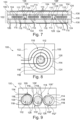
- Figure 8 illustrates a plan view of a component carrier 100 with a single embedded inductor 108 according to another exemplary embodiment.
- the embodiment of Figure 8 is similar to the component carrier 100 of Figure 3 .
- Figure 9 illustrates a plan view of a component carrier 100 with three coupled inductors 108, 108', 108" according to another exemplary embodiment.
- the exact geometric shape can be adapted in accordance with a specific application.
Landscapes
- Engineering & Computer Science (AREA)
- Power Engineering (AREA)
- Microelectronics & Electronic Packaging (AREA)
- Manufacturing & Machinery (AREA)
- Coils Or Transformers For Communication (AREA)
Claims (12)
- Bauteilträger (100), wobei der Bauteilträger umfasst:einen Stapel (102), umfassend mindestens eine elektrisch leitfähige Schichtstruktur (104) und mindestens eine elektrisch isolierende Schichtstruktur (106);einen Induktor (108, 108', 108"), der mindestens teilweise in dem Stapel (102) angeordnet ist und eine elektrisch leitfähige Spulenstruktur (110, 110', 110''), die um eine Spulenöffnung (112, 112', 112") gewickelt ist, und einen Magnetkern (114, 114', 114'') umfasst,wobei mindestens ein Teil des Magnetkerns (114, 114', 114") die Spulenöffnung (112, 112', 112'') mindestens teilweise ausfüllt;wobei mindestens ein Teil von mindestens einer der Spulenstruktur (110, 110', 110'') und/oder des Magnetkerns (114, 114', 114'') als eine in den Stapel (102) eingebettete Einlage ausgebildet ist;wobei der Magnetkern (114, 114', 114'') eine Vielzahl von separaten Magnetkörpern umfasst, wobei die Magnetkörper einen sich durch die Spulenöffnung (112, 112', 112'') erstreckenden Magnetstift (126), ein sich seitlich über den Magnetstift (126) hinaus und mindestens teilweise über die Spulenstruktur (110, 110', 110") erstreckendes Magnetblech (124), ein weiteres Magnetblech (124), das sich seitlich über den Magnetstift (126) hinaus und mindestens teilweise über die Spulenstruktur (110, 110', 110'') erstreckt, und mindestens eine Struktur aus Magnetpaste (128) umfasst, wobei der Magnetstift (126) vertikal zwischen dem Magnetblech (124) und dem weiteren Magnetblech (124) eingefasst ist;wobei die Magnetkörper miteinander verbunden sind, um einen offenen Magnetpfad mit einem nicht magnetischen Spalt (130) zu bilden, der zwei benachbarte der Magnetkörper um mindestens 75 µm beabstandet; undwobei der mindestens eine nicht magnetische Spalt (130) entweder einen Luftspalt oder einen mit elektrisch isolierendem Harzmaterial gefüllten Spalt umfasst;wobei die Magnetpaste (128) das Magnetblech (124) mit dem Magnetstift (126) unter Bildung eines geschlossenen Magnetpfads verbindet und der nicht magnetische Spalt (130) durch Beabstandung des weiteren Magnetblechs (124) und des Magnetstifts (126) gebildet wird.
- Bauteilträger (100) nach Anspruch 1, umfassend mindestens eines der folgenden Merkmale:wobei mindestens ein Teil von einem der Spulenstruktur (110) und/oder des Magnetkerns (114) einen Teil des Stapels (102) bildet;wobei die Spulenstruktur (110) miteinander verbundene elektrisch leitfähige Elemente (116) in und/oder auf einer dielektrischen Matrix (118) umfasst, wobei insbesondere die elektrisch leitfähigen Elemente (116) planare Elemente (120) in Ebenen umfassen, die parallel zu einer oder mehreren Ebenen der mindestens einen elektrisch isolierenden Schichtstruktur (106) des Stapels (102) sind, und ein oder mehrere vertikale Elemente (122) umfassen, die die planaren Elemente (120) verbinden und sich senkrecht zu den Ebenen der planaren Elemente (120) erstrecken;wobei die Spulenstruktur (110) eine Ringform, insbesondere eine Kreisringform oder eine Rechteckringform, aufweist;wobei der Magnetkern (114) ein Material umfasst, das eine magnetische Permeabilität von mindestens 10, insbesondere von mindestens 100 aufweist;wobei der Magnetkern (114) ein Ferritmaterial umfasst.
- Bauteilträger (100) nach Anspruch 1,
wobei der mindestens eine nicht magnetische Spalt benachbarte der Magnetkörper um mindestens 150 µm beabstandet. - Bauteilträger (100) nach einem der Ansprüche 1 bis 3,
wobei eine Oberfläche mindestens eines Teils des Magnetkerns (114) eine Rauheit R.a von weniger als 4 µm, insbesondere weniger als 2 µm, insbesondere nicht mehr als 500 nm aufweist. - Bauteilträger (100) nach einem der Ansprüche 1 bis 4, umfassend mindestens einen weiteren Induktor (108, 108', 108''), der mindestens teilweise in dem Stapel (102) angeordnet ist und umfassend eine weitere elektrisch leitfähige Spulenstruktur (110, 110', 110''), die um eine weitere Spulenöffnung (112, 112', 112") gewickelt ist, und einen weiteren Magnetkern (114, 114', 114"), wobei mindestens ein Teil des weiteren Magnetkerns (114, 114', 114'') die weitere Spulenöffnung (112, 112', 112") mindestens teilweise ausfüllt und insbesondere mindestens eines der folgenden Merkmale umfassend:wobei mindestens ein Teil von mindestens einer weiteren Spulenstruktur (110, 110', 110'') und/oder des Magnetkerns (114, 114', 114'') als eine in den Stapel (102) eingebettete Einlage ausgebildet ist;wobei der Induktor (108', 108'') und der mindestens eine weitere Induktor (108, 108', 108'') magnetisch gekoppelt sind;wobei der Induktor (108', 108'') und der mindestens eine weitere Induktor (108, 108', 108") als Transformator ausgebildet sind;wobei mindestens ein Teil der Magnetkerne (114, 114', 114'') des Induktors (108', 108'') und des mindestens einen weiteren Induktors (108, 108', 108'') als integrale Struktur ausgebildet sind, insbesondere als ein gemeinsames Magnetblech (124) ausgebildet sind.
- Bauteilträger (100) nach Anspruch 1,
wobei der Magnetkern (114) mindestens einen weiteren Magnetstift (126) umfasst, der sich parallel zu dem Magnetstift (126) erstreckt, wobei die Spulenstruktur (110) zwischen dem Magnetstift (126) und dem mindestens einen weiteren Magnetstift (126) angeordnet ist. - Bauteilträger (100) nach einem der Ansprüche 1 bis 6, umfassend mindestens ein in den Bauteilträger eingebettetes Bauteil (132).
- Bauteilträger (100) nach Anspruch 7, umfassend mindestens eines der folgenden Merkmale:wobei das mindestens eine Bauteil (132) ein aktives Bauteil oder ein passives Bauteil ist;wobei das mindestens eine Bauteil (132) mindestens eines aus der Gruppe bestehend aus einem Widerstand, einem einstellbaren Widerstand und einem Transistor umfasst;wobei das mindestens eine Bauteil (132) direkt neben der Spulenstruktur (110) angeordnet ist, insbesondere in direktem physischen Kontakt mit der Spulenstruktur (110);wobei das mindestens eine Bauteil (132) zwischen Windungen der Spulenstruktur (110) des Induktors (108) eingebettet ist;wobei das mindestens eine Bauteil (132) in mindestens eines der Gruppe bestehend aus dem Stapel (102), der Spulenstruktur (110) und dem Magnetkern (114) eingebettet ist;wobei das mindestens eine Bauteil ausgewählt ist aus einer Gruppe bestehend aus einem elektronischen Bauteil, einer elektrisch nicht leitfähigen und/oder elektrisch leitfähigen Einlage, einer Wärmeübertragungseinheit, einem Lichtleitelement, einer Energiegewinnungseinheit, einem aktiven elektronischen Bauteil, einem passiven elektronischen Bauteil, einem elektronischen Chip, einer Speichervorrichtung, einem Filter, einer integrierten Schaltung, einem Signalverarbeitungsbauteil, einem Energieverwaltungsbauteil, einem optoelektronischen Schnittstellenelement, einem Spannungswandler, einem kryptografischen Bauteil, einem Sender und/oder Empfänger, einem elektromechanischen Wandler, einem Aktor, einem mikroelektromechanischen System, einem Mikroprozessor, einem Kondensator, einem Widerstand, einer Induktivität, einem Akkumulator, einem Schalter, einer Kamera, einer Antenne, einem magnetischen Element, einem weiteren Bauteilträger und einem Logikchip.
- Bauteilträger (100) nach einem der Ansprüche 1 bis 8, umfassend mindestens eines der folgenden Merkmale:wobei die mindestens eine elektrisch leitfähige Schichtstruktur (104) mindestens eines aus der Gruppe bestehend aus Kupfer, Aluminium, Nickel, Silber, Gold, Palladium und Wolfram umfasst, wobei jedes der genannten Materialien optional mit supraleitendem Material wie Graphen beschichtet ist;wobei die mindestens eine elektrisch isolierende Schichtstruktur (106) mindestens eines aus der Gruppe bestehend aus Harz, insbesondere verstärktem oder unverstärktem Harz, zum Beispiel Epoxidharz oder Bismaleimid-Triazin-Harz, FR.-4, FR.-5, Cyanatester, Polyphenylenderivat, Glas, Prepreg-Material, Polyimid, Polyamid, Flüssigkristallpolymer, Aufbaufilm auf Epoxidbasis, Polytetrafluorethylen, einer Keramik und einem Metalloxid umfasst;wobei der Bauteilträger als eine Platte geformt ist;wobei der Bauteilträger als eines aus der Gruppe bestehend aus einer gedruckten Leiterplatte und einem Substrat ausgebildet ist;wobei der Bauteilträger als ein laminatartiger Bauteilträger ausgebildet ist.
- Elektrische Vorrichtung (150), wobei die elektrische Vorrichtung umfasst:einen Trägerkörper (152), insbesondere eine gedruckte Leiterplatte;einen Bauteilträger (100) nach einem der Ansprüche 1 bis 9, der an und/oder in dem Trägerkörper montiert ist.
- Verfahren zum Herstellen eines Bauteilträgers (100), wobei das Verfahren umfasst:Bereitstellen eines Stapels (102), umfassend mindestens eine elektrisch leitfähige Schichtstruktur (104) und mindestens eine elektrisch isolierende Schichtstruktur (106);Anordnen eines Induktors (108, 108', 108'') mindestens teilweise in dem Stapel (102);Ausbilden des Induktors (108) mit einer elektrisch leitfähigen Spulenstruktur (110, 110', 110''), die um eine Spulenöffnung (112, 112', 112'') gewickelt ist, und mit einem Magnetkern (114, 114', 114''), der eine Vielzahl von separaten Magnetkörpern umfasst, wobei mindestens ein Teil des Magnetkerns (114, 114', 114") die Spulenöffnung (112, 112', 112'') mindestens teilweise ausfüllt;Einbetten mindestens eines Teils von mindestens einer der Spulenstruktur (110, 110', 110'') und/oder des Magnetkerns (114, 114', 114'') als Einlage in den Stapel (102);wobei die Magnetkörper einen sich durch die Spulenöffnung (112, 112', 112") erstreckenden Magnetstift (126), ein sich seitlich über den Magnetstift (126) hinaus und mindestens teilweise über die Spulenstruktur (110, 110', 110") erstreckendes Magnetblech (124), ein weiteres Magnetblech (124), das sich seitlich über den Magnetstift (126) hinaus und mindestens teilweise über die Spulenstruktur (110, 110', 110'') erstreckt, und mindestens eine Struktur aus Magnetpaste (128) umfasst, wobei der Magnetstift (126) vertikal zwischen dem Magnetblech (124) und dem weiteren Magnetblech (124) eingefasst ist;wobei die Magnetkörper miteinander verbunden sind, um einen offenen Magnetpfad mit einem nicht magnetischen Spalt (130) zu bilden, der zwei benachbarte der Magnetkörper um mindestens 75 µm beabstandet; undwobei der mindestens eine nicht magnetische Spalt (130) entweder einen Luftspalt oder einen mit elektrisch isolierendem Harzmaterial gefüllten Spalt umfasst;wobei die Magnetpaste (128) das Magnetblech (124) mit dem Magnetstift (126) unter Bildung eines geschlossenen Magnetpfads verbindet und der nicht magnetische Spalt (130) durch Beabstandung des weiteren Magnetblechs (124) und des Magnetstifts (126) gebildet wird.
- Verfahren nach Anspruch 11, wobei das Verfahren ein Bilden mindestens eines Teils des Magnetkerns (114) durch Laserschneiden eines Magnetkörpers umfasst.
Applications Claiming Priority (1)
| Application Number | Priority Date | Filing Date | Title |
|---|---|---|---|
| US16/048,663 US11398334B2 (en) | 2018-07-30 | 2018-07-30 | Component carrier comprising embedded inductor with an inlay |
Publications (2)
| Publication Number | Publication Date |
|---|---|
| EP3605564A1 EP3605564A1 (de) | 2020-02-05 |
| EP3605564B1 true EP3605564B1 (de) | 2025-03-05 |
Family
ID=67539190
Family Applications (1)
| Application Number | Title | Priority Date | Filing Date |
|---|---|---|---|
| EP19188903.9A Active EP3605564B1 (de) | 2018-07-30 | 2019-07-29 | Komponententräger mit eingebettetem induktor mit einer einlage |
Country Status (3)
| Country | Link |
|---|---|
| US (1) | US11398334B2 (de) |
| EP (1) | EP3605564B1 (de) |
| CN (1) | CN110797172B (de) |
Families Citing this family (27)
| Publication number | Priority date | Publication date | Assignee | Title |
|---|---|---|---|---|
| EP3736839A1 (de) * | 2019-05-06 | 2020-11-11 | AT & S Austria Technologie & Systemtechnik Aktiengesellschaft | Komponententräger mit eingebettetem magnetstapel |
| US20230333337A1 (en) * | 2019-08-08 | 2023-10-19 | At&S Austria Technologie & Systemtechnik Aktiengesellschaft | Component Carrier and Method of Manufacturing the Same |
| US11071206B2 (en) | 2019-10-17 | 2021-07-20 | Infineon Technologies Austria Ag | Electronic system and processor substrate having an embedded power device module |
| US11183934B2 (en) | 2019-10-17 | 2021-11-23 | Infineon Technologies Americas Corp. | Embedded substrate voltage regulators |
| US11147165B2 (en) * | 2019-10-17 | 2021-10-12 | Infineon Technologies Austria Ag | Electronic system and interposer having an embedded power device module |
| CN111128993A (zh) * | 2019-12-18 | 2020-05-08 | 台达电子企业管理(上海)有限公司 | 基板及其所适用的制造方法及功率模块 |
| US12308738B2 (en) | 2019-12-18 | 2025-05-20 | Delta Electronics (Shanghai) Co., Ltd. | Power module |
| EP3840547A1 (de) * | 2019-12-20 | 2021-06-23 | AT & S Austria Technologie & Systemtechnik Aktiengesellschaft | Komponententräger mit eingebetteter magnetischer einlage und integrierter spulenstruktur |
| US12482595B2 (en) | 2019-12-20 | 2025-11-25 | At&S Austria Technologie & Systemtechnik Ag | Component carrier with embedded magnetic inlay and integrated coil structure |
| CN113380516B (zh) | 2020-03-10 | 2024-08-30 | 台达电子企业管理(上海)有限公司 | 耦合电感及功率模块 |
| US11887776B2 (en) * | 2020-06-18 | 2024-01-30 | Texas Instruments Incorporated | Method for manufacturing an integrated transformer with printed core piece |
| DE102020209543A1 (de) * | 2020-07-29 | 2022-02-03 | Robert Bosch Gesellschaft mit beschränkter Haftung | Leiterplatte mit einer ferromagnetischen Schicht |
| US20220068556A1 (en) * | 2020-08-25 | 2022-03-03 | Texas Instruments Incorporated | Transformers with separated magnetic members |
| TWI734616B (zh) * | 2020-09-21 | 2021-07-21 | 矽品精密工業股份有限公司 | 電子封裝件及其製法 |
| US12362295B2 (en) | 2020-09-24 | 2025-07-15 | Intel Corporation | Planar magnetic radial inductors to enable VR disaggregation |
| CN113053849B (zh) * | 2021-03-04 | 2022-02-15 | 珠海越亚半导体股份有限公司 | 集成电感的嵌埋支撑框架、基板及其制作方法 |
| GB2606787B (en) * | 2021-05-19 | 2024-01-10 | Cirrus Logic Int Semiconductor Ltd | Integrated circuits with embedded layers |
| DE102021207599A1 (de) | 2021-07-16 | 2023-01-19 | Volkswagen Aktiengesellschaft | Planartransformator |
| CN115767885A (zh) * | 2021-11-11 | 2023-03-07 | 台达电子工业股份有限公司 | 电子模块组装结构 |
| US12205750B2 (en) * | 2021-11-30 | 2025-01-21 | Dialog Semiconductor (Uk) Limited | 3D MIS-FO hybrid for embedded inductor package structure |
| FR3130445B1 (fr) * | 2021-12-14 | 2024-12-13 | St Microelectronics Grenoble 2 | Composant inductif et procédé de fabrication |
| DE102022205831A1 (de) * | 2022-06-08 | 2023-12-14 | Robert Bosch Gesellschaft mit beschränkter Haftung | Schaltungsträger mit einer ferromagnetischen Schicht |
| US20240047096A1 (en) * | 2022-08-03 | 2024-02-08 | Infineon Technologies Austria Ag | Graphene in electromagnetic systems |
| CN116153638B (zh) * | 2022-09-05 | 2025-10-31 | 广州辰微电子科技有限公司 | 一种平面变压器的制作方法及平面变压器 |
| US20250037923A1 (en) * | 2023-07-27 | 2025-01-30 | Qualcomm Incorporated | Package comprising a substrate with inductors and a magnetic layer |
| US20250166885A1 (en) * | 2023-11-17 | 2025-05-22 | Applied Materials, Inc. | Novel design and process of scalable high impedance components |
| CN120784091A (zh) * | 2024-04-01 | 2025-10-14 | 华为技术有限公司 | 变压器成型方法、变压器和电源 |
Citations (4)
| Publication number | Priority date | Publication date | Assignee | Title |
|---|---|---|---|---|
| US5349743A (en) * | 1991-05-02 | 1994-09-27 | At&T Bell Laboratories | Method of making a multilayer monolithic magnet component |
| US20080078474A1 (en) * | 2006-09-29 | 2008-04-03 | Yutaka Naito | Magnetic core using amorphous soft magnetic alloy |
| US20130093561A1 (en) * | 2011-10-18 | 2013-04-18 | Kabushiki Kaisha Toyota Jidoshokki | Magnetic core and induction device |
| US20130335937A1 (en) * | 2012-06-15 | 2013-12-19 | Medtronic, Inc. | Integrated circuit packaging for implantable medical devices |
Family Cites Families (16)
| Publication number | Priority date | Publication date | Assignee | Title |
|---|---|---|---|---|
| US5267107A (en) * | 1991-06-28 | 1993-11-30 | Seagate Technology, Inc. | Laminated magnetic transducer |
| US5990776A (en) | 1994-12-08 | 1999-11-23 | Jitaru; Ionel | Low noise full integrated multilayers magnetic for power converters |
| JP4238097B2 (ja) * | 2003-09-04 | 2009-03-11 | Tdk株式会社 | コイル部品の製造方法 |
| DE102007028239A1 (de) | 2007-06-20 | 2009-01-02 | Siemens Ag | Monolithisches induktives Bauelement, Verfahren zum Herstellen des Bauelements und Verwendung des Bauelements |
| JP5132353B2 (ja) * | 2008-02-20 | 2013-01-30 | キヤノン株式会社 | 記録装置 |
| US8094458B2 (en) | 2008-03-24 | 2012-01-10 | Microsemi Corporation | Semiconductor package with embedded magnetic component and method of manufacture |
| EP2107577B1 (de) | 2008-03-31 | 2016-10-19 | Würth Elektronik Rot am See GmbH & Co. KG | Induktionsbauteil und Verfahren zu seiner Herstellung |
| US8410576B2 (en) * | 2010-06-16 | 2013-04-02 | National Semiconductor Corporation | Inductive structure and method of forming the inductive structure with an attached core structure |
| US9633772B2 (en) | 2013-03-14 | 2017-04-25 | Gentex Corporation | Solderable planar magnetic components |
| CN103298258B (zh) | 2013-05-21 | 2016-09-21 | 华为技术有限公司 | 电路板及具有该电路板的电源转换装置 |
| US10141107B2 (en) | 2013-10-10 | 2018-11-27 | Analog Devices, Inc. | Miniature planar transformer |
| KR20160114792A (ko) | 2015-03-24 | 2016-10-06 | 삼성전기주식회사 | 코일 내장 집적회로 기판 및 그 제조 방법 |
| DE102016203613A1 (de) | 2016-03-04 | 2017-09-07 | Würth Elektronik GmbH & Co. KG | Elektronisches Bauelement und Verfahren zu dessen Herstellung |
| GB2553822B (en) | 2016-09-15 | 2018-12-26 | Murata Manufacturing Co | DC-DC Converter device |
| EP3340260B1 (de) | 2016-12-22 | 2022-03-23 | AT & S Austria Technologie & Systemtechnik Aktiengesellschaft | Induktor aus komponententrägermaterial mit elektrisch leitfähigen plattenstrukturen |
| CN107256757B (zh) | 2017-06-21 | 2019-02-12 | 苏州华启智能科技有限公司 | 磁芯嵌入pcb的带屏蔽层的耐高温共模电感 |
-
2018
- 2018-07-30 US US16/048,663 patent/US11398334B2/en active Active
-
2019
- 2019-07-29 EP EP19188903.9A patent/EP3605564B1/de active Active
- 2019-07-30 CN CN201910694976.6A patent/CN110797172B/zh active Active
Patent Citations (4)
| Publication number | Priority date | Publication date | Assignee | Title |
|---|---|---|---|---|
| US5349743A (en) * | 1991-05-02 | 1994-09-27 | At&T Bell Laboratories | Method of making a multilayer monolithic magnet component |
| US20080078474A1 (en) * | 2006-09-29 | 2008-04-03 | Yutaka Naito | Magnetic core using amorphous soft magnetic alloy |
| US20130093561A1 (en) * | 2011-10-18 | 2013-04-18 | Kabushiki Kaisha Toyota Jidoshokki | Magnetic core and induction device |
| US20130335937A1 (en) * | 2012-06-15 | 2013-12-19 | Medtronic, Inc. | Integrated circuit packaging for implantable medical devices |
Also Published As
| Publication number | Publication date |
|---|---|
| EP3605564A1 (de) | 2020-02-05 |
| US11398334B2 (en) | 2022-07-26 |
| US20200035396A1 (en) | 2020-01-30 |
| CN110797172B (zh) | 2024-05-07 |
| CN110797172A (zh) | 2020-02-14 |
Similar Documents
| Publication | Publication Date | Title |
|---|---|---|
| EP3605564B1 (de) | Komponententräger mit eingebettetem induktor mit einer einlage | |
| US12002614B2 (en) | Inductor made of component carrier material comprising electrically conductive plate structures | |
| US11792932B2 (en) | Component carrier with embedded magnetic inlay and integrated coil structure | |
| EP3863030A1 (de) | Im wesentlichen ringförmiges magnetisches element mit magnetischen teilchen in einer nichtmagnetischen matrix für komponententräger | |
| US11889629B2 (en) | Component carrier comprising embedded magnet stack | |
| US11366181B2 (en) | Component carrier with integrated flux gate sensor | |
| US11051406B2 (en) | Component carrier with integrated inductor and manufacturing method | |
| US12482595B2 (en) | Component carrier with embedded magnetic inlay and integrated coil structure | |
| US12543267B2 (en) | Magnetic inlay with an adjustable inductance value for a component carrier and a manufacturing method | |
| US12464649B2 (en) | Component carrier with inductive element included in layer build-up, and manufacturing method | |
| US20220377897A1 (en) | Magnetic Inlay With Electrically Conductive Vertical Through Connections for a Component Carrier | |
| US20220377917A1 (en) | Component Carrier With Magnetic Element, Magnetic Inlay, and Manufacturing Method |
Legal Events
| Date | Code | Title | Description |
|---|---|---|---|
| PUAI | Public reference made under article 153(3) epc to a published international application that has entered the european phase |
Free format text: ORIGINAL CODE: 0009012 |
|
| STAA | Information on the status of an ep patent application or granted ep patent |
Free format text: STATUS: THE APPLICATION HAS BEEN PUBLISHED |
|
| AK | Designated contracting states |
Kind code of ref document: A1 Designated state(s): AL AT BE BG CH CY CZ DE DK EE ES FI FR GB GR HR HU IE IS IT LI LT LU LV MC MK MT NL NO PL PT RO RS SE SI SK SM TR |
|
| AX | Request for extension of the european patent |
Extension state: BA ME |
|
| STAA | Information on the status of an ep patent application or granted ep patent |
Free format text: STATUS: REQUEST FOR EXAMINATION WAS MADE |
|
| 17P | Request for examination filed |
Effective date: 20200722 |
|
| RBV | Designated contracting states (corrected) |
Designated state(s): AL AT BE BG CH CY CZ DE DK EE ES FI FR GB GR HR HU IE IS IT LI LT LU LV MC MK MT NL NO PL PT RO RS SE SI SK SM TR |
|
| STAA | Information on the status of an ep patent application or granted ep patent |
Free format text: STATUS: EXAMINATION IS IN PROGRESS |
|
| 17Q | First examination report despatched |
Effective date: 20201117 |
|
| GRAP | Despatch of communication of intention to grant a patent |
Free format text: ORIGINAL CODE: EPIDOSNIGR1 |
|
| STAA | Information on the status of an ep patent application or granted ep patent |
Free format text: STATUS: GRANT OF PATENT IS INTENDED |
|
| INTG | Intention to grant announced |
Effective date: 20241213 |
|
| GRAS | Grant fee paid |
Free format text: ORIGINAL CODE: EPIDOSNIGR3 |
|
| GRAA | (expected) grant |
Free format text: ORIGINAL CODE: 0009210 |
|
| STAA | Information on the status of an ep patent application or granted ep patent |
Free format text: STATUS: THE PATENT HAS BEEN GRANTED |
|
| AK | Designated contracting states |
Kind code of ref document: B1 Designated state(s): AL AT BE BG CH CY CZ DE DK EE ES FI FR GB GR HR HU IE IS IT LI LT LU LV MC MK MT NL NO PL PT RO RS SE SI SK SM TR |
|
| REG | Reference to a national code |
Ref country code: GB Ref legal event code: FG4D |
|
| REG | Reference to a national code |
Ref country code: CH Ref legal event code: EP |
|
| REG | Reference to a national code |
Ref country code: DE Ref legal event code: R096 Ref document number: 602019066773 Country of ref document: DE |
|
| REG | Reference to a national code |
Ref country code: IE Ref legal event code: FG4D |
|
| P01 | Opt-out of the competence of the unified patent court (upc) registered |
Free format text: CASE NUMBER: APP_15219/2025 Effective date: 20250328 |
|
| PG25 | Lapsed in a contracting state [announced via postgrant information from national office to epo] |
Ref country code: RS Free format text: LAPSE BECAUSE OF FAILURE TO SUBMIT A TRANSLATION OF THE DESCRIPTION OR TO PAY THE FEE WITHIN THE PRESCRIBED TIME-LIMIT Effective date: 20250605 |
|
| PG25 | Lapsed in a contracting state [announced via postgrant information from national office to epo] |
Ref country code: FI Free format text: LAPSE BECAUSE OF FAILURE TO SUBMIT A TRANSLATION OF THE DESCRIPTION OR TO PAY THE FEE WITHIN THE PRESCRIBED TIME-LIMIT Effective date: 20250305 |
|
| REG | Reference to a national code |
Ref country code: NL Ref legal event code: MP Effective date: 20250305 |
|
| PG25 | Lapsed in a contracting state [announced via postgrant information from national office to epo] |
Ref country code: ES Free format text: LAPSE BECAUSE OF FAILURE TO SUBMIT A TRANSLATION OF THE DESCRIPTION OR TO PAY THE FEE WITHIN THE PRESCRIBED TIME-LIMIT Effective date: 20250305 |
|
| REG | Reference to a national code |
Ref country code: LT Ref legal event code: MG9D |
|
| PG25 | Lapsed in a contracting state [announced via postgrant information from national office to epo] |
Ref country code: NO Free format text: LAPSE BECAUSE OF FAILURE TO SUBMIT A TRANSLATION OF THE DESCRIPTION OR TO PAY THE FEE WITHIN THE PRESCRIBED TIME-LIMIT Effective date: 20250605 |
|
| PG25 | Lapsed in a contracting state [announced via postgrant information from national office to epo] |
Ref country code: HR Free format text: LAPSE BECAUSE OF FAILURE TO SUBMIT A TRANSLATION OF THE DESCRIPTION OR TO PAY THE FEE WITHIN THE PRESCRIBED TIME-LIMIT Effective date: 20250305 |
|
| PG25 | Lapsed in a contracting state [announced via postgrant information from national office to epo] |
Ref country code: LV Free format text: LAPSE BECAUSE OF FAILURE TO SUBMIT A TRANSLATION OF THE DESCRIPTION OR TO PAY THE FEE WITHIN THE PRESCRIBED TIME-LIMIT Effective date: 20250305 |
|
| PG25 | Lapsed in a contracting state [announced via postgrant information from national office to epo] |
Ref country code: GR Free format text: LAPSE BECAUSE OF FAILURE TO SUBMIT A TRANSLATION OF THE DESCRIPTION OR TO PAY THE FEE WITHIN THE PRESCRIBED TIME-LIMIT Effective date: 20250606 Ref country code: BG Free format text: LAPSE BECAUSE OF FAILURE TO SUBMIT A TRANSLATION OF THE DESCRIPTION OR TO PAY THE FEE WITHIN THE PRESCRIBED TIME-LIMIT Effective date: 20250305 |
|
| REG | Reference to a national code |
Ref country code: AT Ref legal event code: MK05 Ref document number: 1773742 Country of ref document: AT Kind code of ref document: T Effective date: 20250305 |
|
| PG25 | Lapsed in a contracting state [announced via postgrant information from national office to epo] |
Ref country code: NL Free format text: LAPSE BECAUSE OF FAILURE TO SUBMIT A TRANSLATION OF THE DESCRIPTION OR TO PAY THE FEE WITHIN THE PRESCRIBED TIME-LIMIT Effective date: 20250305 |
|
| PG25 | Lapsed in a contracting state [announced via postgrant information from national office to epo] |
Ref country code: SE Free format text: LAPSE BECAUSE OF FAILURE TO SUBMIT A TRANSLATION OF THE DESCRIPTION OR TO PAY THE FEE WITHIN THE PRESCRIBED TIME-LIMIT Effective date: 20250305 |
|
| PG25 | Lapsed in a contracting state [announced via postgrant information from national office to epo] |
Ref country code: SM Free format text: LAPSE BECAUSE OF FAILURE TO SUBMIT A TRANSLATION OF THE DESCRIPTION OR TO PAY THE FEE WITHIN THE PRESCRIBED TIME-LIMIT Effective date: 20250305 |
|
| PG25 | Lapsed in a contracting state [announced via postgrant information from national office to epo] |
Ref country code: PT Free format text: LAPSE BECAUSE OF FAILURE TO SUBMIT A TRANSLATION OF THE DESCRIPTION OR TO PAY THE FEE WITHIN THE PRESCRIBED TIME-LIMIT Effective date: 20250707 |
|
| PGFP | Annual fee paid to national office [announced via postgrant information from national office to epo] |
Ref country code: DE Payment date: 20250724 Year of fee payment: 7 |
|
| PG25 | Lapsed in a contracting state [announced via postgrant information from national office to epo] |
Ref country code: PL Free format text: LAPSE BECAUSE OF FAILURE TO SUBMIT A TRANSLATION OF THE DESCRIPTION OR TO PAY THE FEE WITHIN THE PRESCRIBED TIME-LIMIT Effective date: 20250305 Ref country code: IT Free format text: LAPSE BECAUSE OF FAILURE TO SUBMIT A TRANSLATION OF THE DESCRIPTION OR TO PAY THE FEE WITHIN THE PRESCRIBED TIME-LIMIT Effective date: 20250305 |
|
| PG25 | Lapsed in a contracting state [announced via postgrant information from national office to epo] |
Ref country code: AT Free format text: LAPSE BECAUSE OF FAILURE TO SUBMIT A TRANSLATION OF THE DESCRIPTION OR TO PAY THE FEE WITHIN THE PRESCRIBED TIME-LIMIT Effective date: 20250305 |
|
| PGFP | Annual fee paid to national office [announced via postgrant information from national office to epo] |
Ref country code: FR Payment date: 20250728 Year of fee payment: 7 |
|
| PG25 | Lapsed in a contracting state [announced via postgrant information from national office to epo] |
Ref country code: EE Free format text: LAPSE BECAUSE OF FAILURE TO SUBMIT A TRANSLATION OF THE DESCRIPTION OR TO PAY THE FEE WITHIN THE PRESCRIBED TIME-LIMIT Effective date: 20250305 Ref country code: CZ Free format text: LAPSE BECAUSE OF FAILURE TO SUBMIT A TRANSLATION OF THE DESCRIPTION OR TO PAY THE FEE WITHIN THE PRESCRIBED TIME-LIMIT Effective date: 20250305 |
|
| PG25 | Lapsed in a contracting state [announced via postgrant information from national office to epo] |
Ref country code: RO Free format text: LAPSE BECAUSE OF FAILURE TO SUBMIT A TRANSLATION OF THE DESCRIPTION OR TO PAY THE FEE WITHIN THE PRESCRIBED TIME-LIMIT Effective date: 20250305 |
|
| PG25 | Lapsed in a contracting state [announced via postgrant information from national office to epo] |
Ref country code: SK Free format text: LAPSE BECAUSE OF FAILURE TO SUBMIT A TRANSLATION OF THE DESCRIPTION OR TO PAY THE FEE WITHIN THE PRESCRIBED TIME-LIMIT Effective date: 20250305 |
|
| PG25 | Lapsed in a contracting state [announced via postgrant information from national office to epo] |
Ref country code: IS Free format text: LAPSE BECAUSE OF FAILURE TO SUBMIT A TRANSLATION OF THE DESCRIPTION OR TO PAY THE FEE WITHIN THE PRESCRIBED TIME-LIMIT Effective date: 20250705 |
|
| REG | Reference to a national code |
Ref country code: DE Ref legal event code: R097 Ref document number: 602019066773 Country of ref document: DE |
|
| PLBE | No opposition filed within time limit |
Free format text: ORIGINAL CODE: 0009261 |
|
| STAA | Information on the status of an ep patent application or granted ep patent |
Free format text: STATUS: NO OPPOSITION FILED WITHIN TIME LIMIT |
|
| PG25 | Lapsed in a contracting state [announced via postgrant information from national office to epo] |
Ref country code: DK Free format text: LAPSE BECAUSE OF FAILURE TO SUBMIT A TRANSLATION OF THE DESCRIPTION OR TO PAY THE FEE WITHIN THE PRESCRIBED TIME-LIMIT Effective date: 20250305 |
|
| REG | Reference to a national code |
Ref country code: CH Ref legal event code: L10 Free format text: ST27 STATUS EVENT CODE: U-0-0-L10-L00 (AS PROVIDED BY THE NATIONAL OFFICE) Effective date: 20260114 |
|
| 26N | No opposition filed |
Effective date: 20251208 |
|
| REG | Reference to a national code |
Ref country code: CH Ref legal event code: H13 Free format text: ST27 STATUS EVENT CODE: U-0-0-H10-H13 (AS PROVIDED BY THE NATIONAL OFFICE) Effective date: 20260224 |
|
| PG25 | Lapsed in a contracting state [announced via postgrant information from national office to epo] |
Ref country code: LU Free format text: LAPSE BECAUSE OF NON-PAYMENT OF DUE FEES Effective date: 20250729 |
|
| GBPC | Gb: european patent ceased through non-payment of renewal fee |
Effective date: 20250729 |
|
| REG | Reference to a national code |
Ref country code: BE Ref legal event code: MM Effective date: 20250731 |
|
| PG25 | Lapsed in a contracting state [announced via postgrant information from national office to epo] |
Ref country code: GB Free format text: LAPSE BECAUSE OF NON-PAYMENT OF DUE FEES Effective date: 20250729 |
|
| PG25 | Lapsed in a contracting state [announced via postgrant information from national office to epo] |
Ref country code: BE Free format text: LAPSE BECAUSE OF NON-PAYMENT OF DUE FEES Effective date: 20250731 |
|
| PG25 | Lapsed in a contracting state [announced via postgrant information from national office to epo] |
Ref country code: CH Free format text: LAPSE BECAUSE OF NON-PAYMENT OF DUE FEES Effective date: 20250731 |