EP3607582B1 - Led-bildanzeigevorrichtung - Google Patents
Led-bildanzeigevorrichtung Download PDFInfo
- Publication number
- EP3607582B1 EP3607582B1 EP18718892.5A EP18718892A EP3607582B1 EP 3607582 B1 EP3607582 B1 EP 3607582B1 EP 18718892 A EP18718892 A EP 18718892A EP 3607582 B1 EP3607582 B1 EP 3607582B1
- Authority
- EP
- European Patent Office
- Prior art keywords
- chip
- vdata
- substrate
- led
- transfer substrate
- Prior art date
- Legal status (The legal status is an assumption and is not a legal conclusion. Google has not performed a legal analysis and makes no representation as to the accuracy of the status listed.)
- Active
Links
Images



Classifications
-
- G—PHYSICS
- G09—EDUCATION; CRYPTOGRAPHY; DISPLAY; ADVERTISING; SEALS
- G09F—DISPLAYING; ADVERTISING; SIGNS; LABELS OR NAME-PLATES; SEALS
- G09F9/00—Indicating arrangements for variable information in which the information is built-up on a support by selection or combination of individual elements
- G09F9/30—Indicating arrangements for variable information in which the information is built-up on a support by selection or combination of individual elements in which the desired character or characters are formed by combining individual elements
- G09F9/33—Indicating arrangements for variable information in which the information is built-up on a support by selection or combination of individual elements in which the desired character or characters are formed by combining individual elements being semiconductor devices, e.g. diodes
-
- G—PHYSICS
- G09—EDUCATION; CRYPTOGRAPHY; DISPLAY; ADVERTISING; SEALS
- G09G—ARRANGEMENTS OR CIRCUITS FOR CONTROL OF INDICATING DEVICES USING STATIC MEANS TO PRESENT VARIABLE INFORMATION
- G09G3/00—Control arrangements or circuits, of interest only in connection with visual indicators other than cathode-ray tubes
- G09G3/20—Control arrangements or circuits, of interest only in connection with visual indicators other than cathode-ray tubes for presentation of an assembly of a number of characters, e.g. a page, by composing the assembly by combination of individual elements arranged in a matrix no fixed position being assigned to or needed to be assigned to the individual characters or partial characters
- G09G3/22—Control arrangements or circuits, of interest only in connection with visual indicators other than cathode-ray tubes for presentation of an assembly of a number of characters, e.g. a page, by composing the assembly by combination of individual elements arranged in a matrix no fixed position being assigned to or needed to be assigned to the individual characters or partial characters using controlled light sources
- G09G3/30—Control arrangements or circuits, of interest only in connection with visual indicators other than cathode-ray tubes for presentation of an assembly of a number of characters, e.g. a page, by composing the assembly by combination of individual elements arranged in a matrix no fixed position being assigned to or needed to be assigned to the individual characters or partial characters using controlled light sources using electroluminescent panels
- G09G3/32—Control arrangements or circuits, of interest only in connection with visual indicators other than cathode-ray tubes for presentation of an assembly of a number of characters, e.g. a page, by composing the assembly by combination of individual elements arranged in a matrix no fixed position being assigned to or needed to be assigned to the individual characters or partial characters using controlled light sources using electroluminescent panels semiconductive, e.g. using light-emitting diodes [LED]
-
- H—ELECTRICITY
- H05—ELECTRIC TECHNIQUES NOT OTHERWISE PROVIDED FOR
- H05K—PRINTED CIRCUITS; CASINGS OR CONSTRUCTIONAL DETAILS OF ELECTRIC APPARATUS; MANUFACTURE OF ASSEMBLAGES OF ELECTRICAL COMPONENTS
- H05K3/00—Apparatus or processes for manufacturing printed circuits
- H05K3/10—Apparatus or processes for manufacturing printed circuits in which conductive material is applied to the insulating support in such a manner as to form the desired conductive pattern
- H05K3/12—Apparatus or processes for manufacturing printed circuits in which conductive material is applied to the insulating support in such a manner as to form the desired conductive pattern using thick film techniques, e.g. printing techniques to apply the conductive material or similar techniques for applying conductive paste or ink patterns
- H05K3/1216—Apparatus or processes for manufacturing printed circuits in which conductive material is applied to the insulating support in such a manner as to form the desired conductive pattern using thick film techniques, e.g. printing techniques to apply the conductive material or similar techniques for applying conductive paste or ink patterns by screen printing or stencil printing
-
- H—ELECTRICITY
- H05—ELECTRIC TECHNIQUES NOT OTHERWISE PROVIDED FOR
- H05K—PRINTED CIRCUITS; CASINGS OR CONSTRUCTIONAL DETAILS OF ELECTRIC APPARATUS; MANUFACTURE OF ASSEMBLAGES OF ELECTRICAL COMPONENTS
- H05K3/00—Apparatus or processes for manufacturing printed circuits
- H05K3/10—Apparatus or processes for manufacturing printed circuits in which conductive material is applied to the insulating support in such a manner as to form the desired conductive pattern
- H05K3/12—Apparatus or processes for manufacturing printed circuits in which conductive material is applied to the insulating support in such a manner as to form the desired conductive pattern using thick film techniques, e.g. printing techniques to apply the conductive material or similar techniques for applying conductive paste or ink patterns
- H05K3/1241—Apparatus or processes for manufacturing printed circuits in which conductive material is applied to the insulating support in such a manner as to form the desired conductive pattern using thick film techniques, e.g. printing techniques to apply the conductive material or similar techniques for applying conductive paste or ink patterns by ink-jet printing or drawing by dispensing
- H05K3/125—Apparatus or processes for manufacturing printed circuits in which conductive material is applied to the insulating support in such a manner as to form the desired conductive pattern using thick film techniques, e.g. printing techniques to apply the conductive material or similar techniques for applying conductive paste or ink patterns by ink-jet printing or drawing by dispensing by ink-jet printing
-
- H—ELECTRICITY
- H05—ELECTRIC TECHNIQUES NOT OTHERWISE PROVIDED FOR
- H05K—PRINTED CIRCUITS; CASINGS OR CONSTRUCTIONAL DETAILS OF ELECTRIC APPARATUS; MANUFACTURE OF ASSEMBLAGES OF ELECTRICAL COMPONENTS
- H05K3/00—Apparatus or processes for manufacturing printed circuits
- H05K3/46—Manufacturing multilayer circuits
- H05K3/4644—Manufacturing multilayer circuits by building the multilayer layer by layer, i.e. build-up multilayer circuits
- H05K3/465—Manufacturing multilayer circuits by building the multilayer layer by layer, i.e. build-up multilayer circuits by applying an insulating layer having channels for the next circuit layer
-
- H—ELECTRICITY
- H05—ELECTRIC TECHNIQUES NOT OTHERWISE PROVIDED FOR
- H05K—PRINTED CIRCUITS; CASINGS OR CONSTRUCTIONAL DETAILS OF ELECTRIC APPARATUS; MANUFACTURE OF ASSEMBLAGES OF ELECTRICAL COMPONENTS
- H05K3/00—Apparatus or processes for manufacturing printed circuits
- H05K3/46—Manufacturing multilayer circuits
- H05K3/4644—Manufacturing multilayer circuits by building the multilayer layer by layer, i.e. build-up multilayer circuits
- H05K3/4664—Adding a circuit layer by thick film methods, e.g. printing techniques or by other techniques for making conductive patterns by using pastes, inks or powders
-
- H—ELECTRICITY
- H10—SEMICONDUCTOR DEVICES; ELECTRIC SOLID-STATE DEVICES NOT OTHERWISE PROVIDED FOR
- H10H—INORGANIC LIGHT-EMITTING SEMICONDUCTOR DEVICES HAVING POTENTIAL BARRIERS
- H10H20/00—Individual inorganic light-emitting semiconductor devices having potential barriers, e.g. light-emitting diodes [LED]
- H10H20/80—Constructional details
- H10H20/85—Packages
-
- H—ELECTRICITY
- H10—SEMICONDUCTOR DEVICES; ELECTRIC SOLID-STATE DEVICES NOT OTHERWISE PROVIDED FOR
- H10H—INORGANIC LIGHT-EMITTING SEMICONDUCTOR DEVICES HAVING POTENTIAL BARRIERS
- H10H20/00—Individual inorganic light-emitting semiconductor devices having potential barriers, e.g. light-emitting diodes [LED]
- H10H20/80—Constructional details
- H10H20/85—Packages
- H10H20/857—Interconnections, e.g. lead-frames, bond wires or solder balls
-
- H—ELECTRICITY
- H10—SEMICONDUCTOR DEVICES; ELECTRIC SOLID-STATE DEVICES NOT OTHERWISE PROVIDED FOR
- H10W—GENERIC PACKAGES, INTERCONNECTIONS, CONNECTORS OR OTHER CONSTRUCTIONAL DETAILS OF DEVICES COVERED BY CLASS H10
- H10W90/00—Package configurations
-
- G—PHYSICS
- G09—EDUCATION; CRYPTOGRAPHY; DISPLAY; ADVERTISING; SEALS
- G09G—ARRANGEMENTS OR CIRCUITS FOR CONTROL OF INDICATING DEVICES USING STATIC MEANS TO PRESENT VARIABLE INFORMATION
- G09G2300/00—Aspects of the constitution of display devices
- G09G2300/08—Active matrix structure, i.e. with use of active elements, inclusive of non-linear two terminal elements, in the pixels together with light emitting or modulating elements
- G09G2300/0804—Sub-multiplexed active matrix panel, i.e. wherein one active driving circuit is used at pixel level for multiple image producing elements
-
- G—PHYSICS
- G09—EDUCATION; CRYPTOGRAPHY; DISPLAY; ADVERTISING; SEALS
- G09G—ARRANGEMENTS OR CIRCUITS FOR CONTROL OF INDICATING DEVICES USING STATIC MEANS TO PRESENT VARIABLE INFORMATION
- G09G2310/00—Command of the display device
- G09G2310/02—Addressing, scanning or driving the display screen or processing steps related thereto
- G09G2310/0264—Details of driving circuits
- G09G2310/0297—Special arrangements with multiplexing or demultiplexing of display data in the drivers for data electrodes, in a pre-processing circuitry delivering display data to said drivers or in the matrix panel, e.g. multiplexing plural data signals to one D/A converter or demultiplexing the D/A converter output to multiple columns
Definitions
- the present application relates to the production of an emissive light-emitting diode (LED) image display device, for example a screen for television, computer, smartphone, digital tablet, etc.
- LED emissive light-emitting diode
- an image display device comprising a plurality of elementary electronic chips arranged in a matrix on the same transfer substrate.
- the chips are mounted integral with the transfer substrate and connected to electrical connection elements of the transfer substrate for their control.
- Each chip comprises a stack of an LED and an LED driver circuit and corresponds to a pixel of the device.
- US 2012/080692 A1 discloses an image display device with a transfer substrate with electrical connections and LEDs.
- the first conductive tracks are substantially parallel, and the second conductive tracks are substantially orthogonal to the first tracks.
- each elementary chip of the device said at least one LED of the chip is formed in a first substrate based on a III-V semiconductor, and the control circuit of the chip is formed in a second substrate based on silicon, attached and electrically connected to the first substrate.
- the chip connection terminals are formed on the side of the face of the second substrate opposite to the first substrate.
- each elementary chip is arranged so that the face of its second substrate opposite the first substrate is turned towards the transfer substrate so as to make direct electrical connections between the connection terminals of the chip and the pads. electrical connection of the transfer substrate.
- the transfer substrate comprises at least one electrical connection pad connected to a first conductive track of the transfer substrate, and at least one electrical connection pad connected to a second conductive track of the transfer substrate. transfer substrate.
- each elementary chip comprises a first connection terminal to the substrate intended to receive an adjustment signal from said at least one LED of the chip.
- each elementary chip further comprises a second connection terminal to the substrate intended to receive a selection and / or synchronization signal.
- each elementary chip further comprises third and fourth connection terminals to the substrate intended to respectively receive a high supply potential and a low supply potential of the chip.
- each elementary chip comprises a plurality of LEDs
- the first connection terminal of the chip is intended to receive, for each LED of the chip, an individual adjustment signal from the LED, the adjustment signals.
- individual of the different LEDs of the chip being time multiplexed on said first terminal.
- control circuit of the chip is adapted to demultiplex the signals received on said first terminal and to apply to each LED of the chip a bias signal depending on the individual adjustment signal of the LED received on said first terminal.
- the same elements have been designated by the same references in the various figures and, moreover, the various figures are not drawn to scale. For the sake of clarity, only the elements useful for understanding the embodiments described have been shown and are detailed. In particular, the manufacture of the elementary chips of the display devices described has not been detailed, the manufacture of these chips being within the reach of those skilled in the art from the teachings of the present description.
- the elementary chips of the display devices described each comprising one or more LEDs and a control circuit based on transistors, can be manufactured according to processes identical or similar to those described in the patent application. French n ° 1561421 mentioned above.
- the figure 1 is an electrical diagram of the circuits of an elementary chip 110 of an image display device of the type described in the patent application French n ° 1561421 mentioned above.
- Chip 110 comprises an LED 120, preferably an inorganic LED, for example a gallium nitride LED or based on any other III-V semiconductor suitable for producing an LED.
- the chip 110 further comprises an active circuit 130 for controlling the LED 120, for example a circuit based on transistors, suitable for controlling the emission of light by the LED.
- control circuit 130 and the LED 120 are first formed separately, respectively in and on a silicon substrate for the circuit 130, and on a suitable growth substrate, for example made of sapphire, for the LED 120.
- LED 120 is made so as to have anode and cathode electrical contacts on the side of its face opposite to the growth substrate.
- the control circuit 130 for its part comprises, on the side of a first face of the silicon substrate, electrical connection zones intended to be brought into contact with the anode and cathode contacts of the LED, and, on the side from a second face of the silicon substrate opposite the first face, terminals for connection to an external device for controlling the chip.
- the circuit 130 and the LED 120 are then secured by bonding the face of the LED opposite the growth substrate on the first face of the circuit 130.
- the chip comprising the circuit 130 and the LED 120 is then transferred onto a transfer substrate, for example a passive transfer substrate, comprising electrical connection elements for supplying and controlling the chip.
- a transfer substrate for example a passive transfer substrate, comprising electrical connection elements for supplying and controlling the chip.
- the chip is arranged so that the second face of the circuit 130 of the chip faces the transfer substrate, in order to make direct electrical connections between the connection terminals outside the chip and the pads. electrical connection of the transfer substrate.
- the substrate of growth can further be removed before or after attachment of the chip to the transfer substrate.
- the chip 110 comprises four connection terminals to the outside Vp, Vn, Vsel, and Vdata.
- the terminals Vp and Vn are intended to receive respectively a low supply potential Vp (for example ground) and a high supply potential (that is to say greater than the low supply potential) Vn of the chip.
- the Vsel and Vdata terminals are intended to receive control signals from the chip. More particularly, the Vsel signal is a chip selection signal, and the Vdata signal is a chip brightness level adjustment signal.
- the control circuit 130 of the chip comprises two transistors 131 and 133 and a capacitive element 135, for example a capacitor.
- transistors 131 and 133 are MOS transistors. More specifically, transistor 131 is an N-channel MOS transistor and transistor 133 is a P-channel MOS transistor.
- Transistor 131 has a first conduction node (source or drain in this example) connected to the Vdata terminal, a second conduction node (drain or source in this example) connected to an intermediate node a1 of the chip, and a control node (gate in this example) connected to the terminal Vsel.
- Capacitive element 135 has a first electrode connected to node a1 and a second electrode connected to terminal Vp.
- Transistor 133 has a first conduction node connected to terminal Vp, a second conduction node connected to the anode of LED 120, and a control node connected to node a1.
- the cathode of LED 120 is connected to terminal Vn.
- the transistor 131 is used in switching (on or off) to allow or not the updating of the brightness setting of the LED.
- the transistor 133 operates in linear mode to control the intensity of the current injected into the LED.
- Transistor 131 is closed (turned on) by applying a suitable control signal to terminal Vsel.
- the capacitive element 135 is then charged to a voltage level which is a function of the adjustment signal applied to the Vdata terminal of the chip.
- the level of the adjustment signal Vdata fixes the potential of the node a1, and consequently the intensity of the current injected into the LED by the transistor 133, and therefore the light intensity emitted by the LED.
- Transistor 131 can then be reopened.
- the node a1 then remains at a potential substantially equal to the potential Vdata.
- the current injected into the LED remains substantially constant after the reopening of the transistor 131, and this until the next update of the potential of the node a1.
- a display device may include a plurality of identical or similar elementary chips 110 mounted on a single transfer substrate in a matrix arrangement along rows and columns, the chips being connected to electrical connection elements of the substrate. for their control, and each chip corresponding to a pixel of the display device.
- the pixels of the display device can be controlled simultaneously line by line.
- the chips of the row have their Vsel control terminals connected to the same conductive line control track of the transfer substrate, the chips of separate lines having their Vsel control terminals connected to conductive line control tracks separate from the transfer substrate.
- the chips of the column have their Vdata control terminals connected to a same conductive column control track of the transfer substrate, the chips of separate columns having their Vdata control terminals connected to conductive control tracks separate columns from the transfer substrate.
- one possibility is to provide, for each pixel of the device, several neighboring elementary chips suitable for transmitting in distinct wavelength ranges, for example three elementary chips suitable for transmitting respectively red light, green light and blue light. Each elementary chip then corresponds to a sub-pixel of the device.
- the elementary chips of distinct colors can comprise LEDs of distinct natures adapted to emit in ranges of distinct wavelengths, or LEDs of the same kind surmounted by filters or photoluminescent conversion elements of distinct natures.
- a problem which then arises resides in the number and the density of the electrical connection elements which must be provided on the transfer substrate to enable each sub-pixel of the device to be individually controlled.
- one possibility is to integrate the different sub-pixels of the same pixel of the device on a single elementary chip.
- the figure 2 is an electrical diagram of an elementary chip 210 of a display device in which each elementary chip corresponds to a pixel of the device and integrates three sub-pixels SP r , SP g and SP b adapted to respectively emit red light , green light and blue light.
- Each sub-pixel SP r , SP g , SP b of the chip 210 comprises substantially the same circuit elements as the chip 110 of the figure 1 , namely an LED 120 r , respectively 120 g , respectively 120 b , a selection transistor 131 r , respectively 131 g , respectively 131 b , a current adjustment transistor 133 r , respectively 133 g , respectively 133 b , and a capacitive element 135 r , respectively 135 g , respectively 135 b .
- the chip has six terminals for connection to the outside Vp, Vn, Vsel, Vdata r , Vdata g and Vdata b .
- the terminals Vp and Vn are intended to respectively receive the low supply potentials Vp and high Vn of the chip.
- the terminals Vsel, Vdata r , Vdata g and Vdata b are intended to receive control signals from the chip. More particularly, the signal Vsel is a chip selection signal, and the signals Vdata r , Vdata g and Vdata b are signals for individually adjusting the brightness levels of the LEDs 120 r , 120 g and 120 b respectively.
- Each of the transistors 131 r , 131 g and 131 b has its control node connected to the terminal Vsel.
- the transistor 131 r has a first conduction node connected to the Vdata terminal r and a second conduction node connected to an intermediate node a1 r of the chip
- the transistor 131 g has a first conduction node connected to the Vdata terminal g and a second conduction node connected to an intermediate node a1 g of the chip
- the transistor 131 b has a first conduction node connected to the Vdata terminal b and a second conduction node connected to an intermediate node a1 b of the chip.
- the capacitive element 135 r has a first electrode connected to the node a1 r and a second electrode connected to the terminal Vp
- the capacitive element 135 g has a first electrode connected to the node a1 g and a second electrode connected to the terminal Vp
- the capacitive element 135 b has a first electrode connected to node a1 b and a second electrode connected to terminal Vp.
- Transistor 133 r has a first conduction node connected to terminal Vp, a second conduction node connected to the anode of LED 120 r , and a control node connected to node a1 r
- transistor 133 g has a first conduction node connected to terminal Vp, a second conduction node connected to the anode of LED 120 g , and a control node connected to node a1 g
- transistor 133 b has a first conduction node connected to Vp terminal, a second conduction node connected to the anode of the LED 120b, and a control node connected to node a1 b.
- Each of the LEDs 120 r , 120 g , 120 b has its cathode connected to terminal Vn.
- the 120 r , 120 g and 120 b LEDs are, for example, LEDs of different types suitable for emitting light in distinct wavelength ranges.
- the 120 r , 120 g and 120 b LEDs are of the same nature and emit in the same range of wavelengths, but are surmounted by filters or photoluminescent conversion elements of different natures so that the pixels SP r , SP g and SP b emit in distinct wavelength ranges.
- the operation of the elementary chip 210 is for example similar to what has been described in relation to the figure 1 , with the difference that, in the example of figure 2 , when the elementary chip 210 is selected by applying a suitable control signal to the Vsel terminal, the potentials of the nodes a1 r , a1 g and a1 b are simultaneously updated as a function of the potentials applied to the Vdata terminals r , Vdata g and Vdata b respectively, which leads to simultaneously updating the individual brightness settings of LEDs 120 r , 120 g and 120 b .
- a drawback of the display device of the figure 2 is that the number of electrical connection elements to be provided on the transfer substrate to enable each pixel of the device to be individually controlled remains relatively high, in particular due to the fact that the brightness adjustment signals Vdata r , Vdata g and Vdata b are carried by separate conductive tracks of the transfer substrate.
- each elementary chip integrates several individually controllable sub-pixels, but in which, in each elementary chip, a single connection terminal to the outside. is designed to receive the individual brightness adjustment signals of the various sub-pixels of the chip, the individual brightness adjustment signals of the sub-pixels being time multiplexed on this connection terminal.
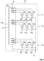
- the figure 3 is a simplified electrical diagram of the circuits of an elementary chip 310 of an example of an image display device according to one embodiment.
- each elementary chip 310 corresponds to a pixel of the device and integrates three sub-pixels SP r , SP g and SP b adapted to respectively emit red light, green light and blue light.
- Each sub-pixel SP r , SP g , SP b of chip 310 comprises substantially the same circuit elements as in the example of figure 2 , namely an LED 120 r , respectively 120 g , respectively 120 b , a selection transistor 131 r , respectively 131 g , respectively 131 b , a current adjustment transistor 133 r , respectively 133 g , respectively 133 b , and a capacitive element 135 r , respectively 135 g , respectively 135 b .
- the transistors 131 r , 131 g , 131 b , 133 r , 133 g , 133 b are N-channel MOS transistors.
- the chip has four connection terminals to the outside Vp, Vn, Vsel and Vdata.
- the terminals Vp and Vn are intended to respectively receive a low supply potential Vp and a high supply potential Vn of the chip.
- the Vsel and Vdata terminals are intended to receive control signals from the chip. More particularly, the Vsel terminal is intended to receive a selection signal from the chip, and the Vdata terminal is intended to receive individual signals for adjusting the brightness levels of the LEDs 120 r , 120 g , 120 b , time multiplexed.
- Chip 310 further comprises an internal selection circuit 312 receiving signal Vsel and supplying selection signals Lr, Lg and Lb applied respectively to the gates of transistors 131 r , 131 g and 131 b . More particularly, in the example shown, the circuit 312 comprises three output nodes Lr, Lg and Lb respectively connected to the gates of transistors 131 r , 131 g and 131 b . Circuit 312 is also connected to terminals Vp and Vn of the chip for its power supply.
- the transistor 131 r has a first conduction node connected to the Vdata terminal and a second conduction node connected to an intermediate node a1 r of the chip
- the transistor 131 g has a first conduction node connected to the Vdata terminal and a second conduction node connected to an intermediate node a1 g of the chip
- transistor 131 b has a first conduction node connected to terminal Vdata and a second conduction node connected to an intermediate node a1 b of the chip.
- the capacitive element 135 r has a first electrode connected to the node a1 r and a second electrode connected to the terminal Vn
- the capacitive element 135 g has a first electrode connected to the node a1 g and a second electrode connected to the terminal Vn
- the capacitive element 135 b has a first electrode connected to node a1 b and a second electrode connected to terminal Vn.
- Transistor 133 r has a first conduction node connected to terminal Vp, a second conduction node connected to the anode of LED 120 r , and a control node connected to node a1 r
- transistor 133 g has a first conduction node connected to terminal Vp, a second conduction node connected to the anode of LED 120 g , and a control node connected to node a1 g
- transistor 133 b has a first conduction node connected to Vp terminal, a second conduction node connected to the anode of the LED 120b, and a control node connected to node a1 b.
- Each of the LEDs 120 r , 120 g , 120 b has its cathode connected to terminal Vn.
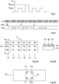
- the figure 4 is a timing diagram illustrating an example of an operating mode of the elementary chip 310 of the figure 3 . More particularly, the figure 4 represents the evolution, as a function of time, of the signals Vdata, Vsel, Lr, Lg and Lb of the chip 310 during a phase of updating the individual brightness levels of the sub-pixels SP r , SP g and SP b of the chip.
- the rising edge of the first pulse of the pulse train marks the start of the pixel update phase, and the rising edge of the last pulse of the pulse train marks the end of the pixel update phase .
- the internal selection circuit 312 controls the closing of the selection transistor 131 r of the sub-pixel SP r , and maintaining in the open state the selection transistors 131 g and 131 b of the sub-pixels SP g and SP b .
- the signal Lr is set to a high state and the signals Lg and Lb are set to a low state.
- the capacitor 135 r of the pixel SP r charges to a voltage level which is a function of the potential applied to the terminal Vdata between the instants t0 and t1 , while the voltage levels of the capacitors 135 g and 135 b remain substantially unchanged.
- the internal selection circuit 312 controls the opening of the selection transistor 131 r of the sub-pixel SP r , the closing of the selection transistor 131 g of the sub-pixel SP g , and the holding at the. open state of the selection transistor 131 b of the sub-pixel SP b .
- signal Lr is set low
- signal Lg is set high
- signal Lb is kept low.
- the capacitor 135 g of the pixel SP g is charged to a voltage level which is a function of the potential applied to the terminal Vdata between the instants t1 and t2 , while the voltage levels of capacitors 135 r and 135 b remain substantially unchanged.
- the internal selection circuit 312 controls the opening of the selection transistor 131 g of the sub-pixel SP g , the closing of the selection transistor 131 b of the sub-pixel SPb, and the keeping in the open state of the selection transistor 131 r of the sub-pixel SP r .
- signal Lg is set low
- signal Lb is set high
- signal Lr is kept low.
- the capacitor 135 b of the pixel SP b charges to a voltage level which is a function of the potential applied to the terminal Vdata between the instants t2 and t3 , while the voltage levels of the capacitors 135 r and 135 g remain substantially unchanged.
- the instant t3 marks the end of the pixel updating phase. From the instant t3, the luminosity levels of the LEDs 120 r , 120 g and 120 b remain substantially unchanged until the next update of the pixel.
- the level of the signal Vdata varies between the instants t0 and t3, in stages at each new rising edge of the signal Vsel.
- the portion of the signal Vdata between the instants t0 and t1 corresponds to an individual signal for adjusting the LED 120 r of the sub-pixel SP r
- the portion of the signal Vdata between the instants t1 and t2 corresponds to an individual signal for adjusting the LED 120 g of the sub-pixel SP g
- the portion of the signal Vdata between the instants t2 and t3 corresponds to an individual signal for adjusting the LED 120 g of the sub-pixel SP g .
- the individual control signals Vdata r , Vdata g and Vdata b are therefore time multiplexed on the Vdata terminal.
- the assembly comprising the internal selection circuit 312, the transistors 131 r , 131 g , 131 b , 133 r , 133 g , 133 b and the capacitors 135 r , 135 g and 135 b of the chip constitutes a suitable control circuit in demultiplexing the individual adjustment signals received at the Vdata terminal, and in applying to each LED of the chip a bias signal (a current in this example) which is a function of the individual adjustment signal of the LED.
- circuit 312 may include a two-stage pulse counter associated with decoding gates, and with a reset mechanism, for example obtained by an envelope detector type assembly receiving the signal as input. Vsel.
- the elementary chips 310 of the display device of the figure 3 can be arranged in a matrix according to rows and columns, and interconnected in rows and columns so as to allow simultaneous row-by-row control of the pixels of the device.
- each elementary chip 310 comprises a single Vdata terminal to receive the individual adjustment signals of all the sub-pixels of the chip.
- each elementary chip 310 comprises only four connection terminals to the outside, that is to say no more than in an elementary chip of the type described in relation to the figure 1 (including a single LED).
- This allows in particular, compared to the example of the figure 2 , to reduce the number of electrical connection elements to be provided on the transfer substrate.
- the individual brightness adjustment signals Vdata r , Vdata g and Vdata b of the different sub-pixels of the same chip 310 are carried by a same conductive track of the transfer substrate.
- each elementary chip comprises a single pixel divided into three sub-pixels adapted to be emitted in three distinct wavelength ranges.
- each elementary chip can comprise a single pixel divided into a number of sub-pixels other than three.
- each elementary chip can comprise several pixels which may or may not be divided into sub-pixels of distinct colors.
- the embodiments described are particularly suited to the production of a so-called multi-view display device, that is to say in which the image to be displayed is divided into macropixels each comprising a plurality of pixels corresponding to different views of the scene that it is desired to reproduce.
- the different pixels of the same macropixel correspond respectively to the same pixel of different images of the same scene, taken from different viewing angles.
- a multi-view display device can for example be used in applications in which it is desired to give the user an impression of a three-dimensional visualization.
- the figure 5 is a simplified electrical diagram of the circuits of an elementary chip 510 of an example of a multi-view image display device according to one embodiment.
- each elementary chip 510 corresponds to a macropixel of the device, comprising n pixels P1, P2, ... Pn intended to respectively display the same point of n different images, corresponding for example to n different views of the same scene , where n is an integer greater than 1, for example included in the range going from 2 to 50.
- each pixel Pi of the macropixel with i integer ranging from 1 to n, comprises several sub-pixels adapted to be emitted in distinct wavelength ranges, so as to allow the display of color images. More particularly, in the example shown, each pixel Pi comprises three sub-pixels SP r , SP g and SP b adapted to respectively emit red light, green light and blue light.
- the 510 chip of the figure 5 includes four connection terminals to the outside Vp, Vn, Vsel and Vdata.
- Each sub-pixel SP r , SP g , SP b of the chip 510 comprises substantially the same circuit elements as in the example of figure 3 , arranged substantially in the same way.
- the selection transistors 131 r , 131 g , 131 b of all the pixels P1, P2, ... Pn of the chip 510 i.e. n * 3 selection transistors
- Chip 510 further includes an internal selection circuit 512 similar to circuit 312 of the figure 3 , receiving the signal Vsel and supplying, for each pixel Pi, selection signals Lr Pi , Lg Pi and Lb Pi applied respectively to the gates of the transistors 131 r , 131 g and 131 b of the pixel Pi.
- the circuit 512 includes n * 3 output nodes Lr P1 , Lg P1 , Lb P1 , Lr P2 , Lg P2 , Lb P2 , ... Lr Pn , Lg Pn , Lb Pn respectively connected to the gates of the selection transistors 131 r , 131 g and 131 b of the n pixels Pi of the chip.
- Circuit 512 is also connected to terminals Vp and Vn of the chip for its power supply.
- the operation of the elementary chip 510 of the figure 5 is similar to what has been described above in relation to figures 3 and 4 . More particularly, in the example of figure 5 , during a phase of updating the n * 3 sub-pixels of the chip, the n * 3 individual adjustment signals of the n * 3 LEDs of the chip are time multiplexed on the Vdata terminal of the chip.
- the selection signal Vsel comprises for example a train of (n * 3) +1 pulses to synchronize the demultiplexing of the Vdata signal inside the chip.
- the elementary chips 510 of the display device of the figure 5 can be arranged in a matrix according to rows and columns, and interconnected in rows and columns so as to allow simultaneous row-by-row control of the macropixels of the device.
- the figure 6 is a simplified electrical diagram of the circuits of an elementary chip 610 of an example of a multi-view image display device according to one embodiment.
- the 610 chip of the figure 6 differs from the 510 chip of the figure 5 mainly in that in chip 610 the individual setting signals of the different LEDs of the chip are received as digital data serialized on the Vdata connection terminal of the chip.
- the elementary chip 610 of the figure 6 corresponds to a macropixel of the display device, comprising n pixels P1, P2, ... Pn each comprising three sub-pixels SP r , SP g and SP b each comprising an individually adjustable LED.
- each sub-pixel SP r comprises an LED 120 r arranged to emit red light
- each sub-pixel SP g comprises an LED 120 g arranged to emit green light
- each sub-pixel SP b comprises an LED 120 b arranged to emit blue light.
- all of the LEDs on the chip have their cathode region connected to the low power supply terminal Vn of the chip.
- the chip 610 further comprises a control circuit 620 connected to the connection terminals outside Vsel, Vdata, Vp and Vn of the chip.
- the circuit 620 is adapted to decode the serialized digital signal received by the chip on its Vdata terminal, and to apply to each LED of the chip a bias signal depending on the individual adjustment signal of the LED received in digital form on the Vdata terminal.
- the circuit 620 comprises n * 3 output nodes or nodes for supplying bias signals, respectively connected to the anode contact regions of the n * 3 LEDs of the chip.
- the circuit 620 comprises, for each pixel Pi of the chip, an output node out Pi connected to the anode of the LED 120 r of the pixel Pi, an output node outg Pi connected to the anode of the LED 120 g of pixel Pi, and an outb Pi output node connected to the anode of the LED 120 b of the pixel Pi.
- the circuit 620 is for example adapted to supply to each LED of the chip, via its output node connected to the anode of the LED, a bias current depending on the individual adjustment signal of the LED received on the Vdata terminal of the chip.
- control circuit 620 replaces the control circuit formed by the internal selection circuit 512, the transistors 131 r , 131 g , 131 b , 133 r , 133 g , 133 b and the capacitors 135 r , 135 g and 135 b in the example of figure 5 .
- the figures 7 and 8 are timing diagrams illustrating an example of an operating mode of the elementary chip 610 of the figure 6 . More particularly, the figure 7 partially represents the signal applied to the terminal Vsel of the chip during a phase of updating the individual brightness levels of the sub-pixels of the chip.
- the figure 8 represents the evolution of internal chip CLK and SYNC signals generated by circuit 620 from signal Vsel. The figure 8 furthermore represents the evolution of the Vdata signal applied to the chip during a phase of updating the individual brightness levels of the sub-pixels of the chip.
- the signal Vsel is a three-level signal, a low level (0), an intermediate level TH CLK greater than the low level, and a high level TH SYNC greater than the intermediate level.
- the signal Vsel transmitted to the chip 610 during a phase of updating the individual brightness levels of the sub-pixels of the chip corresponds to the superposition of a periodic clock signal CLK, corresponding to a succession of pulses regularly spaced at intermediate level TH CLK , and a synchronization signal SYNC, corresponding to a succession of high level pulses TH SYNC .
- the control circuit 620 comprises a stage (not detailed) for separating the signals CLK and SYNC, receiving on an input node the signal Vsel and supplying on two separate output nodes two binary signals corresponding respectively to the signal CLK and to the signal SYNC .
- the separation of the signals CLK and SYNC is carried out by means of two comparators comparing the signal Vsel respectively with the threshold TH CLK and with the threshold TH SYNC , the outputs of the comparators respectively supplying the signal CLK and the signal SYNC.
- the CLK signal is a clock signal making it possible to clock the decoding operations of the serialized digital signal transmitted on the Vdata terminal
- the SYNC signal is a synchronization signal making it possible to indicate to the control circuit 620 that it is going to receive signals. data to be decoded on the Vdata terminal of the chip.
- nbSP 3 sub-pixels, ie 15 LEDs to be updated.
- the number of bits of bits on which each individual LED adjustment signal is coded may be different from 4, for example included in the range from 4 to 16 bits.
- the macropixel update sequence begins with the application of a double pulse of the SYNC signal to the Vsel terminal.
- the circuit 620 On receipt of this double pulse of the SYNC signal, the circuit 620 is informed that serialized binary data for updating the macropixel will be transmitted to its Vdata terminal.
- a counter internal to the circuit 620, clocked by the clock signal CLK, is for example reinitialized at this step.
- Circuit 620 is thus informed that a second train of n * nbits of data will be transmitted to it via the Vdata terminal, corresponding to the individual signals of adjustment of the n sub-pixels of a second color of the macropixel, for example the n sub-pixels SP g of the macropixel.
- a new single pulse of the SYNC signal is applied to the terminal Vsel, so as to inform the circuit 620 that a third train of n * nbits of data will be transmitted to it via the terminal Vdata, corresponding to the individual signals for adjusting the n sub-pixels of a third color of the macropixel, for example the n sub-pixels SP b of the macropixel.
- the SYNC signal may include a single single pulse at the start of the update phase, the data then being transmitted as an uninterrupted stream of n * nbSP * nbits, or 60 bits in the example considered.
- circuit 620 For each individual adjustment signal of an LED of the macropixel, a digital-to-analog conversion of the individual adjustment signal received on the Vdata terminal can be implemented. A bias signal (current or voltage) depending on the adjustment signal received is then applied to the LED.
- circuit 620 comprises a digital-to-analog converter, ie n * nbSP digital-to-analog converters in total.
- the analog output signal of the digital-to-analog converter associated with an LED is for example directly applied to the anode of the LED.
- the output signal from the digital-to-analog converter is used to set a controllable current source injecting current into the LED.
- the elementary chips 610 of the display device of the figure 6 can be arranged in a matrix according to rows and columns, and interconnected in rows and columns so as to allow simultaneous row-by-row control of the macropixels of the device.
- each elementary chip 510 or 610 of the device are monochromatic pixels of the type described in relation to the figure 1 , that is to say not divided into sub-pixels suitable for emitting in distinct wavelength ranges.
- the variant of figure 6 (digital transmission of the adjustment signals) can be adapted to the case where the elementary chip 610 comprises, as in the example of figure 3 , a single pixel divided into several sub-pixels adapted to emit in distinct wavelength ranges.
- the figures 9A, 9B and 9C are schematic views of an elementary chip of an image display device of the type described above.
- the chip comprises 6 pixels P1, P2, P3, P4, P5 and P6 each comprising three sub-pixels SP r , SP g and SP b adapted to emit in three distinct wavelength ranges.
- the figure 9A is a top view of the chip
- the figure 9B is a sectional view of the chip according to the plan 9B-9B of the figure 9A
- the figure 9C is a bottom view of the chip.
- the chip comprises a first substrate 901, for example based on a III-V semiconductor, in which the LEDs 120 r , 120 g , 120 b of the chip are formed, and, attached and electrically connected to the substrate 901, a second substrate 903, for example in silicon, in which the control circuit of the chip is formed.
- the chip comprises, on the side of the face of the substrate 903 opposite the substrate 901, a zone electrical connection 905 comprising the four connection terminals to the outside Vp, Vn, Vsel and Vdata of the chip.
- each macropixel is surmounted by one or more lenses, not shown, adapted to achieve the angular separation, along the x axis, of the beams corresponding to the different pixels of the macropixel.
- the sub-pixels SP r , SP g , SP b of the pixel are arranged in a strip, aligned along a y axis substantially orthogonal to the x axis, and substantially parallel to the columns of the macropixel matrix.
- One advantage of this configuration is that it makes it possible to avoid an angular separation of the different colors of the same pixel, due to the presence of the angular separation lens (s) along the x axis above the macropixel.
- the figure 10 is a schematic and partial top view of an example of a transfer substrate for the elementary chips of a display device of the type described above in relation to the figures 3 to 8 .
- a portion of the transfer substrate corresponding to a three-row by two-column sub-matrix of the display device, has been shown.
- the transfer substrate comprises, for example, a support plate or sheet 1010 made of an insulating material, for example glass or plastic.
- the transfer substrate further comprises electrical connection elements, and in particular conductive tracks and conductive pads, formed by printing on the upper face of the support plate 1010. These electrical connection elements are formed by printing a succession of conductive and insulating levels on the upper face of the support plate 1010.
- the electrical connection elements are for example formed by a printing process of inkjet printing type, by screen printing, by rotogravure, or by any other adapted method.
- the transfer substrate of the figure 10 is a passive substrate, that is to say it comprises only electrical connection elements.
- Active display device control circuits suitable for supplying and controlling the elementary chips of the device via the electrical connection elements of the transfer substrate, are for example connected to the electrical connection elements of the transfer substrate to the transfer substrate. periphery of the transfer substrate.
- the manufacture of the transfer substrate comprises the following three successive printing steps.
- a plurality of conductive tracks are printed on the upper face of the support plate 1010 which are substantially parallel to the direction of the lines of the display device. More particularly, in this example, during the first printing step, two conductive tracks L1 and L2 extending over substantially the entire length of the lines of the display device are printed for each line of the display device.
- the tracks L1 are intended to convey the control signals Vsel of the various lines of pixels or of macropixels of the device.
- the tracks L2 are intended to distribute the low supply potential Vn of the device.
- the conductive elements printed during this first printing step define a first conductive level M1 of the transfer substrate.
- certain portions of the conductive tracks L1 and L2 are covered with an insulating material 1012, so as to allow the subsequent printing of conductive tracks extending above the tracks L1 and L2, without creating a short circuit with the L1 and L2 tracks.
- a plurality of conductive tracks are printed on the upper face of the support plate 1010 which are substantially parallel to the direction of the columns of the display device. More particularly, in this example, during the third printing step, two conductive tracks C1 and C2 are printed for each column of the display device, extending over substantially the entire length of the columns of the display device.
- the tracks C1 are intended to convey the Vdata control signals of the various columns of pixels or of macropixels of the device.
- the tracks C2 are intended to distribute the high power supply potential Vp of the device.
- the conductive tracks C1 and C2 are isolated from the conductive tracks L1 and L2 by the insulating regions 1012 formed in the previous step.
- conductive areas P1, P2, P3 and P4 intended to receive respectively the connection terminals Vsel, Vp, Vn and Vdata of the chip. including pixel or macropixel.
- the range P1 is connected to the conductive track L1 associated with the line to which the pixel or the macropixel belongs.
- the pad P1 extends over and in contact with the upper face of the track L1 in an area of the track L1 not coated by the insulating material 1012.
- the pad P2 is connected to the conductive track C2 associated with the column. to which the pixel or macropixel belongs.
- the area P2 is contiguous to the conductive track C2.
- the range P3 is connected to the conductive track L2 associated with the line to which the pixel or the macropixel belongs. For this, the range P3 extends over and in contact with the upper face of track L2, in a zone of track L2 not coated by the insulating material 1012.
- the pad P4 is connected to the conductive track C1 associated with the column to which the pixel or the macropixel belongs. For this, the range P4 is contiguous to the conductive track C1.
- the conductive tracks and areas printed during the third step define a second conductive level M2 of the transfer substrate. In the third printing step, alignment patterns for the transfer of the chips can additionally be printed in the second conductive level M2.
- An advantage of the transfer substrate described in relation to the figure 10 is that all the conductive areas for connection of the transfer substrate to the elementary chips of the display device (the areas P1, P2, P3 and P4) are formed in the same conductive level, during the same printing step. It follows that the areas P1, P2, P3 and P4 associated with the same pixel or macropixel of the device can be formed very close to each other, for example distant two by two of less than 20 ⁇ m, preferably distant two by two. less than 10 ⁇ m, preferably two by two less than 5 ⁇ m apart, which would be difficult or even impossible to obtain if the conductive areas P1 and P3 were formed during the first printing step, and the conductive areas P2 and P4 during the third printing step. Indeed, the printing resolution of the conductive patterns during a single printing step is relatively high, while there may be a relatively large alignment error between conductive patterns formed during different printing steps. .
- the embodiment of the figure 10 makes it possible to maximize the conductive surface occupied by the areas P1, P2, P3, P4 in the areas of connection of the substrate to the elementary chips, which makes it possible to facilitate the subsequent step of mounting the elementary chips on the transfer substrate, by releasing in particular the constraints of alignment of the chips with respect to the transfer substrate.
- the transfer substrate described in relation to the figure 10 can be used not only in a display device of the type described in connection with the figures 3 to 8 , in which each elementary chip of the device comprises several individually adjustable LEDs, but also in a display device of the type described in relation to the figure 1 in which each elementary chip of the device comprises a single LED.
- each elementary chip of the display device comprises four connection terminals to the outside
- the transfer substrate described in relation to the figure 10 can be adapted to a display device in which each elementary chip comprises a number of connection terminals to the outside other than four.
Landscapes
- Engineering & Computer Science (AREA)
- Manufacturing & Machinery (AREA)
- Microelectronics & Electronic Packaging (AREA)
- Physics & Mathematics (AREA)
- General Physics & Mathematics (AREA)
- Theoretical Computer Science (AREA)
- Computer Hardware Design (AREA)
- Control Of Indicators Other Than Cathode Ray Tubes (AREA)
- Control Of El Displays (AREA)
Claims (11)
- Emissive Anzeigevorrichtung, die Folgendes aufweist:ein Transfersubstrat (1010) mit elektrischen Verbindungselementen (L1, L2, C1, C2, P1, P2, P3, P4); undeine Vielzahl von Halbleiterchips (310; 510; 610), die an dem Transfersubstrat befestigt und mit den elektrischen Verbindungselementen des Transfersubstrats zu ihrer Steuerung verbunden sind, wobei jeder Chip Folgendes umfasst:- mindestens eine LED (120; 120r, 120g, 120b);- eine Vielzahl von Anschlüssen (Vdata, Vsel, Vp, Vn) zur Verbindung mit dem Transfersubstrat; und- eine auf Transistoren basierende Steuerschaltung, die in der Lage ist, an die mindestens eine LED ein Vorspannungssignal in Abhängigkeit von Signalen anzulegen, die an den Anschlüssen der Verbindung des Chips mit dem Transfersubstrat empfangen werden,wobei das Transfersubstrat (1010) eine isolierende Platte aufweist, wobei die elektrischen Verbindungselemente des Transfersubstrats durch Drucken einer ersten leitenden Ebene, gefolgt von einer isolierenden Ebene, gefolgt von einer zweiten leitenden Ebene, auf eine Oberfläche der Platte gebildet werden, wobei die Elemente der elektrischen Verbindung des Transfersubstrats Folgendes aufweisen:eine Vielzahl von ersten Leiterbahnen (L1, L2), die in der ersten Leiterebene ausgebildet sind;eine Vielzahl von zweiten Leiterbahnen (C1, C2), die in der zweiten Leiterebene ausgebildet sind; undfür jeden Chip der Vorrichtung eine Vielzahl von elektrischen Verbindungsbereichen (P1, P2, P3, P4), die jeweils mit den Verbindungsanschlüssen (Vdata, Vsel, Vp, Vn) des Chips verbunden sind, wobei diese Bereiche alle in der zweiten Leiterebene ausgebildet sind,und wobei in jedem Elementar-Chip (310; 510; 610) der Vorrichtung die mindestens eine LED des Chips in einem ersten Substrat (901) auf der Basis eines III-V-Halbleiters ausgebildet ist und elektrische Anoden- und Kathodenkontakte auf der Seite einer ersten Oberfläche des ersten Substrats aufweist, und wobei die Chipsteuerschaltung in einem zweiten Substrat (903) auf der Basis von Silizium ausgebildet ist und elektrische Verbindungsbereiche auf der Seite einer ersten Oberfläche des zweiten Substrats aufweist, wobei die erste Oberfläche des zweiten Substrats an die erste Oberfläche des ersten Substrats angrenzt, und zwar derart, dass die Anoden- und Kathodenkontakte der LED direkt mit den elektrischen Verbindungsbereichen der Steuerschaltung in Kontakt gebracht werden, wobei die Verbindungsanschlüsse (Vdata, Vsel, Vp, Vn) des Chips auf der Seite einer zweiten Oberfläche des zweiten Substrats (903) gegenüber der ersten Oberfläche des zweiten Substrats (903) ausgebildet sind.
- Vorrichtung nach Anspruch 1, wobei die ersten Leiterbahnen im Wesentlichen parallel sind und wobei die zweiten Leiterbahnen im Wesentlichen orthogonal zu den ersten Leiterbahnen sind.
- Vorrichtung nach Anspruch 1 oder 2, wobei jeder Elementar-Chip so angeordnet ist, dass die dem ersten Substrat (901) gegenüberliegende Oberfläche seines zweiten Substrats (903) dem Transfersubstrat (1010) zugewandt ist, um direkte elektrische Verbindungen zwischen den Anschlüssen (Vdata, Vsel, Vp, Vn) des Chips und den elektrischen Anschlussbereichen (P1, P2, P3, P4) des Transfersubstrats zu bilden.
- Vorrichtung nach einem der Ansprüche 1 bis 3, wobei das Transfersubstrat (1010) für jeden Chip der Vorrichtung mindestens einen elektrischen Verbindungsbereich (P1, P3), der mit einer ersten Leiterbahn (L1, L2) des Transfersubstrats verbunden ist, und mindestens einen elektrischen Verbindungsbereich (P2, P4), der mit einer zweiten Leiterbahn (C1, C2) des Transfersubstrats verbunden ist, aufweist.
- Vorrichtung nach einem der Ansprüche 1 bis 4, dadurch gekennzeichnet, dass jeder Elementar-Chip einen ersten Anschluss (Vdata) zur Verbindung mit dem Übertragungssubstrat aufweist, der dazu bestimmt ist, ein Signal (Vdata; Vdatar, Vdatag, Vdatab) zur Einstellung der mindestens einen LED des Chips zu empfangen.
- Vorrichtung nach Anspruch 5, wobei jeder Elementar-Chip außerdem einen zweiten Anschluss (Vsel) zur Verbindung mit dem Transfersubstrat aufweist, der dazu bestimmt ist, ein Auswahl- und/oder Synchronisationssignal zu empfangen.
- Vorrichtung nach Anspruch 5 oder 6, wobei jeder Elementar-Chip außerdem einen dritten (Vp) und einen vierten (Vn) Anschluss zur Verbindung mit dem Transfersubstrat aufweist, die dazu bestimmt sind, ein hohes Stromversorgungspotenzial bzw. ein niedriges Stromversorgungspotenzial des Chips zu empfangen.
- Vorrichtung nach einem der Ansprüche 5 bis 7, wobei jeder Elementar-Chip eine Vielzahl von LEDs aufweist und wobei der erste Verbindungsanschluss (Vdata) des Chips dazu bestimmt ist, für jede LED des Chips ein individuelles Signal zum Einstellen der LED zu empfangen, wobei die individuellen Signale zum Einstellen der verschiedenen LEDs des Chips an dem ersten Anschluss (Vdata) zeitlich gemultiplext werden.
- Vorrichtung nach Anspruch 8, wobei in jedem Elementar-Chip die Chip-Steuerschaltung in der Lage ist, die an dem ersten Anschluss empfangenen Signale zu demultiplexen und an jede LED des Chips ein Vorspannungssignal anzulegen, das eine Funktion des an dem ersten Anschluss (Vdata) empfangenen individuellen LED-Einstellsignals ist.
- Verfahren zur Herstellung der Anzeigevorrichtung nach einem der Ansprüche 1 bis 9, das die folgenden aufeinanderfolgenden Schritte aufweist:a) Aufdrucken der ersten Leiterebene auf die Oberfläche der Isolierplatte, um die Vielzahl der ersten Leiterbahnen (L1, L2) zu bilden;b) Drucken der isolierenden Ebene auf die erste Leiterebene; undc) Bedrucken der isolierenden Ebene mit der zweiten Leiterebene, um die Vielzahl der elektrischen Verbindungsbereiche (P1, P2, P3, P4) zu bilden.
- Verfahren nach Anspruch 10, wobei die Druckschritte a), b) und c) durch ein Tintenstrahldruck-, Siebdruck- oder Rotationstiefdruckverfahren ausgeführt werden.
Priority Applications (1)
| Application Number | Priority Date | Filing Date | Title |
|---|---|---|---|
| EP21199575.8A EP3965153B1 (de) | 2017-04-05 | 2018-04-04 | Led-emissionsbildanzeigevorrichtung |
Applications Claiming Priority (2)
| Application Number | Priority Date | Filing Date | Title |
|---|---|---|---|
| FR1752955A FR3065117B1 (fr) | 2017-04-05 | 2017-04-05 | Dispositif d'affichage d'images emissif a led |
| PCT/FR2018/050844 WO2018185434A1 (fr) | 2017-04-05 | 2018-04-04 | Dispositif d'affichage d'images emissif a led |
Related Child Applications (1)
| Application Number | Title | Priority Date | Filing Date |
|---|---|---|---|
| EP21199575.8A Division EP3965153B1 (de) | 2017-04-05 | 2018-04-04 | Led-emissionsbildanzeigevorrichtung |
Publications (2)
| Publication Number | Publication Date |
|---|---|
| EP3607582A1 EP3607582A1 (de) | 2020-02-12 |
| EP3607582B1 true EP3607582B1 (de) | 2021-10-20 |
Family
ID=59699765
Family Applications (2)
| Application Number | Title | Priority Date | Filing Date |
|---|---|---|---|
| EP21199575.8A Active EP3965153B1 (de) | 2017-04-05 | 2018-04-04 | Led-emissionsbildanzeigevorrichtung |
| EP18718892.5A Active EP3607582B1 (de) | 2017-04-05 | 2018-04-04 | Led-bildanzeigevorrichtung |
Family Applications Before (1)
| Application Number | Title | Priority Date | Filing Date |
|---|---|---|---|
| EP21199575.8A Active EP3965153B1 (de) | 2017-04-05 | 2018-04-04 | Led-emissionsbildanzeigevorrichtung |
Country Status (5)
| Country | Link |
|---|---|
| US (1) | US11373978B2 (de) |
| EP (2) | EP3965153B1 (de) |
| CN (2) | CN117276258A (de) |
| FR (1) | FR3065117B1 (de) |
| WO (1) | WO2018185434A1 (de) |
Cited By (1)
| Publication number | Priority date | Publication date | Assignee | Title |
|---|---|---|---|---|
| EP3940686A2 (de) * | 2020-06-22 | 2022-01-19 | Global Technologies Co., Ltd. | Hintergrundbeleuchtungsvorrichtung für anzeige und integrierte schaltung zur stromsteuerung davon |
Families Citing this family (6)
| Publication number | Priority date | Publication date | Assignee | Title |
|---|---|---|---|---|
| KR102271828B1 (ko) * | 2020-06-22 | 2021-07-01 | 주식회사 글로벌테크놀로지 | 디스플레이를 위한 백라이트 장치 |
| CN114447012B (zh) * | 2020-10-30 | 2025-11-04 | 启耀光电股份有限公司 | 透光显示模块的制造方法 |
| FR3119931B1 (fr) | 2021-02-17 | 2024-04-05 | Commissariat Energie Atomique | Dispositif optoélectronique et procédé de fabrication d'un tel dispositif |
| FR3120988B1 (fr) | 2021-03-18 | 2023-03-24 | Commissariat Energie Atomique | Dispositif d'affichage émissif à LED |
| FR3121569B1 (fr) * | 2021-03-31 | 2023-03-17 | Aledia | Pixel d'affichage à diode électroluminescente |
| US20230055746A1 (en) * | 2021-08-17 | 2023-02-23 | X Display Company Technology Limited | Displays with dual-pixel drivers |
Citations (5)
| Publication number | Priority date | Publication date | Assignee | Title |
|---|---|---|---|---|
| DE19950839A1 (de) * | 1999-10-21 | 2001-05-23 | Fraunhofer Ges Forschung | Vorrichtung zur Ansteuerung der Anzeigeelemente eines Anzeigeelementenarrays und Verfahren zur Herstellung derselben |
| US20050128767A1 (en) * | 2003-12-10 | 2005-06-16 | Bily Wang | Light source structure of light emitting diode |
| US20120080692A1 (en) * | 2010-10-05 | 2012-04-05 | Sony Corporation | Display panel, display device, illumination panel and illumination device, and methods of manufacturing display panel and illumination panel |
| US20160258588A1 (en) * | 2013-12-20 | 2016-09-08 | Osram Opto Semiconductors Gmbh | Optoelectronic Semiconductor Component and Adaptive Headlight for a Motor Vehicle |
| US20170061867A1 (en) * | 2015-08-25 | 2017-03-02 | X-Celeprint Limited | Bit-plane pulse width modulated digital display system |
Family Cites Families (17)
| Publication number | Priority date | Publication date | Assignee | Title |
|---|---|---|---|---|
| FR1561421A (de) | 1968-02-12 | 1969-03-28 | ||
| JP2002244576A (ja) * | 2001-02-21 | 2002-08-30 | Sony Corp | 表示装置の製造方法、表示装置及び液晶表示装置 |
| JP2003309293A (ja) * | 2002-04-17 | 2003-10-31 | Sony Corp | 半導体発光素子パッケージ、表示装置、発光素子の除去方法及び発光素子の検査方法 |
| KR100658615B1 (ko) * | 2004-04-29 | 2006-12-15 | 삼성에스디아이 주식회사 | 발광 표시 패널 및 발광 표시 장치 |
| JP5078416B2 (ja) * | 2006-04-27 | 2012-11-21 | キヤノン株式会社 | 反射型液晶表示装置及び反射型液晶表示装置用の基板 |
| KR20070109532A (ko) * | 2006-05-11 | 2007-11-15 | 삼성전자주식회사 | 백라이트와 백라이트 구동 방법 및 이를 포함한액정표시장치 |
| EP1956580A1 (de) | 2006-12-18 | 2008-08-13 | AGC Flat Glass Europe SA | Anzeigetafel |
| JP5643720B2 (ja) * | 2011-06-30 | 2014-12-17 | 株式会社沖データ | ディスプレイモジュール及びその製造方法と表示装置 |
| JP6124573B2 (ja) * | 2011-12-20 | 2017-05-10 | キヤノン株式会社 | 表示装置 |
| EP2626901A1 (de) * | 2012-02-10 | 2013-08-14 | Oki Data Corporation | Lichtemittierende Halbleitervorrichtung, Bildanzeigevorrichtung, mobiles Endgerät, Blickfeldanzeigevorrichtung, Bildprojektor, Datenhelm und Bilderzeugungsvorrichtung |
| JP5821685B2 (ja) * | 2012-02-22 | 2015-11-24 | セイコーエプソン株式会社 | 電気光学装置および電子機器 |
| KR101924996B1 (ko) * | 2012-03-29 | 2018-12-05 | 삼성디스플레이 주식회사 | 유기 발광 표시 장치 |
| SG11201406630YA (en) * | 2012-04-20 | 2015-01-29 | Sharp Kk | Display device |
| US9084326B2 (en) | 2012-09-13 | 2015-07-14 | Qualcomm Incorporated | Method and apparatus for LED forward voltage measurement for optimum system efficiency |
| CN103310729B (zh) * | 2013-05-29 | 2015-05-27 | 京东方科技集团股份有限公司 | 发光二极管像素单元电路和显示面板 |
| ES2807219T3 (es) | 2014-07-03 | 2021-02-22 | Signify Holding Bv | Cadenas de luz divisibles y métodos para dividir cadenas de luz |
| WO2017053477A1 (en) | 2015-09-25 | 2017-03-30 | Sxaymiq Technologies Llc | Hybrid micro-driver architectures having time multiplexing for driving displays |
-
2017
- 2017-04-05 FR FR1752955A patent/FR3065117B1/fr not_active Expired - Fee Related
-
2018
- 2018-04-04 US US16/499,289 patent/US11373978B2/en active Active
- 2018-04-04 WO PCT/FR2018/050844 patent/WO2018185434A1/fr not_active Ceased
- 2018-04-04 CN CN202311471755.5A patent/CN117276258A/zh active Pending
- 2018-04-04 EP EP21199575.8A patent/EP3965153B1/de active Active
- 2018-04-04 CN CN201880037190.0A patent/CN110720142B/zh active Active
- 2018-04-04 EP EP18718892.5A patent/EP3607582B1/de active Active
Patent Citations (5)
| Publication number | Priority date | Publication date | Assignee | Title |
|---|---|---|---|---|
| DE19950839A1 (de) * | 1999-10-21 | 2001-05-23 | Fraunhofer Ges Forschung | Vorrichtung zur Ansteuerung der Anzeigeelemente eines Anzeigeelementenarrays und Verfahren zur Herstellung derselben |
| US20050128767A1 (en) * | 2003-12-10 | 2005-06-16 | Bily Wang | Light source structure of light emitting diode |
| US20120080692A1 (en) * | 2010-10-05 | 2012-04-05 | Sony Corporation | Display panel, display device, illumination panel and illumination device, and methods of manufacturing display panel and illumination panel |
| US20160258588A1 (en) * | 2013-12-20 | 2016-09-08 | Osram Opto Semiconductors Gmbh | Optoelectronic Semiconductor Component and Adaptive Headlight for a Motor Vehicle |
| US20170061867A1 (en) * | 2015-08-25 | 2017-03-02 | X-Celeprint Limited | Bit-plane pulse width modulated digital display system |
Non-Patent Citations (2)
| Title |
|---|
| CHRISTOPHER A BOWER ET AL: "Transfer-Printed Microscale Integrated Circuits for High Performance Display Backplanes", IEEE TRANSACTIONS ON COMPONENTS, PACKAGING AND MANUFACTURING TECHNOLOGY, IEEE, USA, vol. 1, no. 12, 1 December 2011 (2011-12-01), pages 1916 - 1922, XP011391217, ISSN: 2156-3950, DOI: 10.1109/TCPMT.2011.2128324 * |
| CHRISTOPHER A. BOWER ET AL: "Emissive displays with transfer-printed assemblies of 8??[mu]m???15??[mu]m inorganic light-emitting diodes", PHOTONICS RESEARCH, vol. 5, no. 2, 1 April 2017 (2017-04-01), pages A23, XP055407047, ISSN: 2327-9125, DOI: 10.1364/PRJ.5.000A23 * |
Cited By (1)
| Publication number | Priority date | Publication date | Assignee | Title |
|---|---|---|---|---|
| EP3940686A2 (de) * | 2020-06-22 | 2022-01-19 | Global Technologies Co., Ltd. | Hintergrundbeleuchtungsvorrichtung für anzeige und integrierte schaltung zur stromsteuerung davon |
Also Published As
| Publication number | Publication date |
|---|---|
| CN110720142B (zh) | 2023-10-17 |
| FR3065117A1 (fr) | 2018-10-12 |
| EP3965153A1 (de) | 2022-03-09 |
| US11373978B2 (en) | 2022-06-28 |
| WO2018185434A1 (fr) | 2018-10-11 |
| FR3065117B1 (fr) | 2019-07-05 |
| EP3965153B1 (de) | 2023-07-05 |
| CN110720142A (zh) | 2020-01-21 |
| CN117276258A (zh) | 2023-12-22 |
| EP3607582A1 (de) | 2020-02-12 |
| US20210111157A1 (en) | 2021-04-15 |
Similar Documents
| Publication | Publication Date | Title |
|---|---|---|
| EP3607583B1 (de) | Led-emissionsbildanzeigevorrichtung | |
| EP3607582B1 (de) | Led-bildanzeigevorrichtung | |
| EP3401958B1 (de) | Herstellungsverfahren einer led-anzeigevorrichtung | |
| EP3655990B1 (de) | Optoelektronische vorrichtung | |
| EP3655944B1 (de) | Optoelektronische vorrichtung | |
| WO2023110604A1 (fr) | Pixel d'affichage a diodes electroluminescentes pour ecran d'affichage | |
| EP4060650A1 (de) | Led-emissionsanzeigevorrichtung | |
| WO2022207730A1 (fr) | Pixel d'affichage a diode electroluminescente | |
| EP3679604B1 (de) | Verfahren zur herstellung einer led-basierten emittierenden anzeigevorrichtung | |
| EP4371157B1 (de) | Interaktive anzeigevorrichtung | |
| EP4138128B1 (de) | Bilderfassungsvorrichtung | |
| FR3137485A1 (fr) | Pixel d'affichage comprenant des sources électroluminescentes | |
| US12587766B2 (en) | Image pixel and image sensor device including thereof | |
| EP3921871B1 (de) | Elektrolumineszente anzeigevorrichtung | |
| EP3799126B1 (de) | Animationsvorrichtung von analogen leuchtflächen, und entsprechendes herstellungsverfahren | |
| FR3150040A1 (fr) | Pixel d'affichage comprenant des diodes électroluminescentes pour un écran d'affichage | |
| EP4167282A1 (de) | Verfahren zur herstellung einer optoelektronischen vorrichtung | |
| FR3150639A1 (fr) | Ecran d'affichage comportant des pixels d'affichage comprenant des sources luminescentes |
Legal Events
| Date | Code | Title | Description |
|---|---|---|---|
| STAA | Information on the status of an ep patent application or granted ep patent |
Free format text: STATUS: UNKNOWN |
|
| STAA | Information on the status of an ep patent application or granted ep patent |
Free format text: STATUS: THE INTERNATIONAL PUBLICATION HAS BEEN MADE |
|
| PUAI | Public reference made under article 153(3) epc to a published international application that has entered the european phase |
Free format text: ORIGINAL CODE: 0009012 |
|
| STAA | Information on the status of an ep patent application or granted ep patent |
Free format text: STATUS: REQUEST FOR EXAMINATION WAS MADE |
|
| 17P | Request for examination filed |
Effective date: 20191017 |
|
| AK | Designated contracting states |
Kind code of ref document: A1 Designated state(s): AL AT BE BG CH CY CZ DE DK EE ES FI FR GB GR HR HU IE IS IT LI LT LU LV MC MK MT NL NO PL PT RO RS SE SI SK SM TR |
|
| AX | Request for extension of the european patent |
Extension state: BA ME |
|
| DAV | Request for validation of the european patent (deleted) | ||
| DAX | Request for extension of the european patent (deleted) | ||
| GRAP | Despatch of communication of intention to grant a patent |
Free format text: ORIGINAL CODE: EPIDOSNIGR1 |
|
| STAA | Information on the status of an ep patent application or granted ep patent |
Free format text: STATUS: GRANT OF PATENT IS INTENDED |
|
| GRAJ | Information related to disapproval of communication of intention to grant by the applicant or resumption of examination proceedings by the epo deleted |
Free format text: ORIGINAL CODE: EPIDOSDIGR1 |
|
| STAA | Information on the status of an ep patent application or granted ep patent |
Free format text: STATUS: REQUEST FOR EXAMINATION WAS MADE |
|
| GRAP | Despatch of communication of intention to grant a patent |
Free format text: ORIGINAL CODE: EPIDOSNIGR1 |
|
| STAA | Information on the status of an ep patent application or granted ep patent |
Free format text: STATUS: GRANT OF PATENT IS INTENDED |
|
| INTG | Intention to grant announced |
Effective date: 20210125 |
|
| GRAJ | Information related to disapproval of communication of intention to grant by the applicant or resumption of examination proceedings by the epo deleted |
Free format text: ORIGINAL CODE: EPIDOSDIGR1 |
|
| INTG | Intention to grant announced |
Effective date: 20200218 |
|
| STAA | Information on the status of an ep patent application or granted ep patent |
Free format text: STATUS: REQUEST FOR EXAMINATION WAS MADE |
|
| GRAP | Despatch of communication of intention to grant a patent |
Free format text: ORIGINAL CODE: EPIDOSNIGR1 |
|
| STAA | Information on the status of an ep patent application or granted ep patent |
Free format text: STATUS: GRANT OF PATENT IS INTENDED |
|
| INTC | Intention to grant announced (deleted) | ||
| INTG | Intention to grant announced |
Effective date: 20210330 |
|
| GRAJ | Information related to disapproval of communication of intention to grant by the applicant or resumption of examination proceedings by the epo deleted |
Free format text: ORIGINAL CODE: EPIDOSDIGR1 |
|
| GRAP | Despatch of communication of intention to grant a patent |
Free format text: ORIGINAL CODE: EPIDOSNIGR1 |
|
| GRAC | Information related to communication of intention to grant a patent modified |
Free format text: ORIGINAL CODE: EPIDOSCIGR1 |
|
| INTG | Intention to grant announced |
Effective date: 20210705 |
|
| GRAS | Grant fee paid |
Free format text: ORIGINAL CODE: EPIDOSNIGR3 |
|
| GRAA | (expected) grant |
Free format text: ORIGINAL CODE: 0009210 |
|
| STAA | Information on the status of an ep patent application or granted ep patent |
Free format text: STATUS: THE PATENT HAS BEEN GRANTED |
|
| AK | Designated contracting states |
Kind code of ref document: B1 Designated state(s): AL AT BE BG CH CY CZ DE DK EE ES FI FR GB GR HR HU IE IS IT LI LT LU LV MC MK MT NL NO PL PT RO RS SE SI SK SM TR |
|
| REG | Reference to a national code |
Ref country code: GB Ref legal event code: FG4D Free format text: NOT ENGLISH |
|
| REG | Reference to a national code |
Ref country code: CH Ref legal event code: EP |
|
| REG | Reference to a national code |
Ref country code: DE Ref legal event code: R096 Ref document number: 602018025302 Country of ref document: DE |
|
| REG | Reference to a national code |
Ref country code: IE Ref legal event code: FG4D Free format text: LANGUAGE OF EP DOCUMENT: FRENCH |
|
| REG | Reference to a national code |
Ref country code: AT Ref legal event code: REF Ref document number: 1440628 Country of ref document: AT Kind code of ref document: T Effective date: 20211115 |
|
| REG | Reference to a national code |
Ref country code: LT Ref legal event code: MG9D |
|
| REG | Reference to a national code |
Ref country code: NL Ref legal event code: MP Effective date: 20211020 |
|
| REG | Reference to a national code |
Ref country code: AT Ref legal event code: MK05 Ref document number: 1440628 Country of ref document: AT Kind code of ref document: T Effective date: 20211020 |
|
| PG25 | Lapsed in a contracting state [announced via postgrant information from national office to epo] |
Ref country code: RS Free format text: LAPSE BECAUSE OF FAILURE TO SUBMIT A TRANSLATION OF THE DESCRIPTION OR TO PAY THE FEE WITHIN THE PRESCRIBED TIME-LIMIT Effective date: 20211020 Ref country code: LT Free format text: LAPSE BECAUSE OF FAILURE TO SUBMIT A TRANSLATION OF THE DESCRIPTION OR TO PAY THE FEE WITHIN THE PRESCRIBED TIME-LIMIT Effective date: 20211020 Ref country code: FI Free format text: LAPSE BECAUSE OF FAILURE TO SUBMIT A TRANSLATION OF THE DESCRIPTION OR TO PAY THE FEE WITHIN THE PRESCRIBED TIME-LIMIT Effective date: 20211020 Ref country code: BG Free format text: LAPSE BECAUSE OF FAILURE TO SUBMIT A TRANSLATION OF THE DESCRIPTION OR TO PAY THE FEE WITHIN THE PRESCRIBED TIME-LIMIT Effective date: 20220120 Ref country code: AT Free format text: LAPSE BECAUSE OF FAILURE TO SUBMIT A TRANSLATION OF THE DESCRIPTION OR TO PAY THE FEE WITHIN THE PRESCRIBED TIME-LIMIT Effective date: 20211020 |
|
| PG25 | Lapsed in a contracting state [announced via postgrant information from national office to epo] |
Ref country code: IS Free format text: LAPSE BECAUSE OF FAILURE TO SUBMIT A TRANSLATION OF THE DESCRIPTION OR TO PAY THE FEE WITHIN THE PRESCRIBED TIME-LIMIT Effective date: 20220220 Ref country code: SE Free format text: LAPSE BECAUSE OF FAILURE TO SUBMIT A TRANSLATION OF THE DESCRIPTION OR TO PAY THE FEE WITHIN THE PRESCRIBED TIME-LIMIT Effective date: 20211020 Ref country code: PT Free format text: LAPSE BECAUSE OF FAILURE TO SUBMIT A TRANSLATION OF THE DESCRIPTION OR TO PAY THE FEE WITHIN THE PRESCRIBED TIME-LIMIT Effective date: 20220221 Ref country code: PL Free format text: LAPSE BECAUSE OF FAILURE TO SUBMIT A TRANSLATION OF THE DESCRIPTION OR TO PAY THE FEE WITHIN THE PRESCRIBED TIME-LIMIT Effective date: 20211020 Ref country code: NO Free format text: LAPSE BECAUSE OF FAILURE TO SUBMIT A TRANSLATION OF THE DESCRIPTION OR TO PAY THE FEE WITHIN THE PRESCRIBED TIME-LIMIT Effective date: 20220120 Ref country code: NL Free format text: LAPSE BECAUSE OF FAILURE TO SUBMIT A TRANSLATION OF THE DESCRIPTION OR TO PAY THE FEE WITHIN THE PRESCRIBED TIME-LIMIT Effective date: 20211020 Ref country code: LV Free format text: LAPSE BECAUSE OF FAILURE TO SUBMIT A TRANSLATION OF THE DESCRIPTION OR TO PAY THE FEE WITHIN THE PRESCRIBED TIME-LIMIT Effective date: 20211020 Ref country code: HR Free format text: LAPSE BECAUSE OF FAILURE TO SUBMIT A TRANSLATION OF THE DESCRIPTION OR TO PAY THE FEE WITHIN THE PRESCRIBED TIME-LIMIT Effective date: 20211020 Ref country code: GR Free format text: LAPSE BECAUSE OF FAILURE TO SUBMIT A TRANSLATION OF THE DESCRIPTION OR TO PAY THE FEE WITHIN THE PRESCRIBED TIME-LIMIT Effective date: 20220121 Ref country code: ES Free format text: LAPSE BECAUSE OF FAILURE TO SUBMIT A TRANSLATION OF THE DESCRIPTION OR TO PAY THE FEE WITHIN THE PRESCRIBED TIME-LIMIT Effective date: 20211020 |
|
| REG | Reference to a national code |
Ref country code: DE Ref legal event code: R097 Ref document number: 602018025302 Country of ref document: DE |
|
| PG25 | Lapsed in a contracting state [announced via postgrant information from national office to epo] |
Ref country code: SM Free format text: LAPSE BECAUSE OF FAILURE TO SUBMIT A TRANSLATION OF THE DESCRIPTION OR TO PAY THE FEE WITHIN THE PRESCRIBED TIME-LIMIT Effective date: 20211020 Ref country code: SK Free format text: LAPSE BECAUSE OF FAILURE TO SUBMIT A TRANSLATION OF THE DESCRIPTION OR TO PAY THE FEE WITHIN THE PRESCRIBED TIME-LIMIT Effective date: 20211020 Ref country code: RO Free format text: LAPSE BECAUSE OF FAILURE TO SUBMIT A TRANSLATION OF THE DESCRIPTION OR TO PAY THE FEE WITHIN THE PRESCRIBED TIME-LIMIT Effective date: 20211020 Ref country code: EE Free format text: LAPSE BECAUSE OF FAILURE TO SUBMIT A TRANSLATION OF THE DESCRIPTION OR TO PAY THE FEE WITHIN THE PRESCRIBED TIME-LIMIT Effective date: 20211020 Ref country code: DK Free format text: LAPSE BECAUSE OF FAILURE TO SUBMIT A TRANSLATION OF THE DESCRIPTION OR TO PAY THE FEE WITHIN THE PRESCRIBED TIME-LIMIT Effective date: 20211020 Ref country code: CZ Free format text: LAPSE BECAUSE OF FAILURE TO SUBMIT A TRANSLATION OF THE DESCRIPTION OR TO PAY THE FEE WITHIN THE PRESCRIBED TIME-LIMIT Effective date: 20211020 |
|
| PLBE | No opposition filed within time limit |
Free format text: ORIGINAL CODE: 0009261 |
|
| STAA | Information on the status of an ep patent application or granted ep patent |
Free format text: STATUS: NO OPPOSITION FILED WITHIN TIME LIMIT |
|
| 26N | No opposition filed |
Effective date: 20220721 |
|
| PG25 | Lapsed in a contracting state [announced via postgrant information from national office to epo] |
Ref country code: AL Free format text: LAPSE BECAUSE OF FAILURE TO SUBMIT A TRANSLATION OF THE DESCRIPTION OR TO PAY THE FEE WITHIN THE PRESCRIBED TIME-LIMIT Effective date: 20211020 |
|
| PG25 | Lapsed in a contracting state [announced via postgrant information from national office to epo] |
Ref country code: SI Free format text: LAPSE BECAUSE OF FAILURE TO SUBMIT A TRANSLATION OF THE DESCRIPTION OR TO PAY THE FEE WITHIN THE PRESCRIBED TIME-LIMIT Effective date: 20211020 |
|
| REG | Reference to a national code |
Ref country code: CH Ref legal event code: PL |
|
| REG | Reference to a national code |
Ref country code: BE Ref legal event code: MM Effective date: 20220430 |
|
| PG25 | Lapsed in a contracting state [announced via postgrant information from national office to epo] |
Ref country code: MC Free format text: LAPSE BECAUSE OF FAILURE TO SUBMIT A TRANSLATION OF THE DESCRIPTION OR TO PAY THE FEE WITHIN THE PRESCRIBED TIME-LIMIT Effective date: 20211020 Ref country code: LU Free format text: LAPSE BECAUSE OF NON-PAYMENT OF DUE FEES Effective date: 20220404 Ref country code: LI Free format text: LAPSE BECAUSE OF NON-PAYMENT OF DUE FEES Effective date: 20220430 Ref country code: CH Free format text: LAPSE BECAUSE OF NON-PAYMENT OF DUE FEES Effective date: 20220430 |
|
| PG25 | Lapsed in a contracting state [announced via postgrant information from national office to epo] |
Ref country code: BE Free format text: LAPSE BECAUSE OF NON-PAYMENT OF DUE FEES Effective date: 20220430 |
|
| PG25 | Lapsed in a contracting state [announced via postgrant information from national office to epo] |
Ref country code: IE Free format text: LAPSE BECAUSE OF NON-PAYMENT OF DUE FEES Effective date: 20220404 |
|
| PG25 | Lapsed in a contracting state [announced via postgrant information from national office to epo] |
Ref country code: IT Free format text: LAPSE BECAUSE OF FAILURE TO SUBMIT A TRANSLATION OF THE DESCRIPTION OR TO PAY THE FEE WITHIN THE PRESCRIBED TIME-LIMIT Effective date: 20211020 |
|
| PG25 | Lapsed in a contracting state [announced via postgrant information from national office to epo] |
Ref country code: MK Free format text: LAPSE BECAUSE OF FAILURE TO SUBMIT A TRANSLATION OF THE DESCRIPTION OR TO PAY THE FEE WITHIN THE PRESCRIBED TIME-LIMIT Effective date: 20211020 Ref country code: CY Free format text: LAPSE BECAUSE OF FAILURE TO SUBMIT A TRANSLATION OF THE DESCRIPTION OR TO PAY THE FEE WITHIN THE PRESCRIBED TIME-LIMIT Effective date: 20211020 |
|
| PG25 | Lapsed in a contracting state [announced via postgrant information from national office to epo] |
Ref country code: HU Free format text: LAPSE BECAUSE OF FAILURE TO SUBMIT A TRANSLATION OF THE DESCRIPTION OR TO PAY THE FEE WITHIN THE PRESCRIBED TIME-LIMIT; INVALID AB INITIO Effective date: 20180404 |
|
| PG25 | Lapsed in a contracting state [announced via postgrant information from national office to epo] |
Ref country code: TR Free format text: LAPSE BECAUSE OF FAILURE TO SUBMIT A TRANSLATION OF THE DESCRIPTION OR TO PAY THE FEE WITHIN THE PRESCRIBED TIME-LIMIT Effective date: 20211020 |
|
| PG25 | Lapsed in a contracting state [announced via postgrant information from national office to epo] |
Ref country code: MT Free format text: LAPSE BECAUSE OF FAILURE TO SUBMIT A TRANSLATION OF THE DESCRIPTION OR TO PAY THE FEE WITHIN THE PRESCRIBED TIME-LIMIT Effective date: 20211020 |
|
| REG | Reference to a national code |
Ref country code: DE Ref legal event code: R079 Ref document number: 602018025302 Country of ref document: DE Free format text: PREVIOUS MAIN CLASS: H01L0025075000 Ipc: H10H0029240000 |
|
| PGFP | Annual fee paid to national office [announced via postgrant information from national office to epo] |
Ref country code: DE Payment date: 20250417 Year of fee payment: 8 |
|
| PGFP | Annual fee paid to national office [announced via postgrant information from national office to epo] |
Ref country code: GB Payment date: 20250424 Year of fee payment: 8 |
|
| PGFP | Annual fee paid to national office [announced via postgrant information from national office to epo] |
Ref country code: FR Payment date: 20250422 Year of fee payment: 8 |