EP3609062A1 - Stromwandlungsvorrichtung - Google Patents
Stromwandlungsvorrichtung Download PDFInfo
- Publication number
- EP3609062A1 EP3609062A1 EP17904457.3A EP17904457A EP3609062A1 EP 3609062 A1 EP3609062 A1 EP 3609062A1 EP 17904457 A EP17904457 A EP 17904457A EP 3609062 A1 EP3609062 A1 EP 3609062A1
- Authority
- EP
- European Patent Office
- Prior art keywords
- transmission period
- power
- conversion device
- power conversion
- control unit
- Prior art date
- Legal status (The legal status is an assumption and is not a legal conclusion. Google has not performed a legal analysis and makes no representation as to the accuracy of the status listed.)
- Granted
Links
Images







Classifications
-
- H—ELECTRICITY
- H02—GENERATION; CONVERSION OR DISTRIBUTION OF ELECTRIC POWER
- H02M—APPARATUS FOR CONVERSION BETWEEN AC AND AC, BETWEEN AC AND DC, OR BETWEEN DC AND DC, AND FOR USE WITH MAINS OR SIMILAR POWER SUPPLY SYSTEMS; CONVERSION OF DC OR AC INPUT POWER INTO SURGE OUTPUT POWER; CONTROL OR REGULATION THEREOF
- H02M1/00—Details of apparatus for conversion
- H02M1/08—Circuits specially adapted for the generation of control voltages for semiconductor devices incorporated in static converters
- H02M1/083—Circuits specially adapted for the generation of control voltages for semiconductor devices incorporated in static converters for the ignition at the zero crossing of the voltage or the current
-
- H—ELECTRICITY
- H02—GENERATION; CONVERSION OR DISTRIBUTION OF ELECTRIC POWER
- H02M—APPARATUS FOR CONVERSION BETWEEN AC AND AC, BETWEEN AC AND DC, OR BETWEEN DC AND DC, AND FOR USE WITH MAINS OR SIMILAR POWER SUPPLY SYSTEMS; CONVERSION OF DC OR AC INPUT POWER INTO SURGE OUTPUT POWER; CONTROL OR REGULATION THEREOF
- H02M1/00—Details of apparatus for conversion
- H02M1/08—Circuits specially adapted for the generation of control voltages for semiconductor devices incorporated in static converters
- H02M1/084—Circuits specially adapted for the generation of control voltages for semiconductor devices incorporated in static converters using a control circuit common to several phases of a multi-phase system
-
- H—ELECTRICITY
- H02—GENERATION; CONVERSION OR DISTRIBUTION OF ELECTRIC POWER
- H02M—APPARATUS FOR CONVERSION BETWEEN AC AND AC, BETWEEN AC AND DC, OR BETWEEN DC AND DC, AND FOR USE WITH MAINS OR SIMILAR POWER SUPPLY SYSTEMS; CONVERSION OF DC OR AC INPUT POWER INTO SURGE OUTPUT POWER; CONTROL OR REGULATION THEREOF
- H02M1/00—Details of apparatus for conversion
- H02M1/08—Circuits specially adapted for the generation of control voltages for semiconductor devices incorporated in static converters
- H02M1/088—Circuits specially adapted for the generation of control voltages for semiconductor devices incorporated in static converters for the simultaneous control of series or parallel connected semiconductor devices
- H02M1/096—Circuits specially adapted for the generation of control voltages for semiconductor devices incorporated in static converters for the simultaneous control of series or parallel connected semiconductor devices the power supply of the control circuit being connected in parallel to the main switching element
-
- H—ELECTRICITY
- H02—GENERATION; CONVERSION OR DISTRIBUTION OF ELECTRIC POWER
- H02M—APPARATUS FOR CONVERSION BETWEEN AC AND AC, BETWEEN AC AND DC, OR BETWEEN DC AND DC, AND FOR USE WITH MAINS OR SIMILAR POWER SUPPLY SYSTEMS; CONVERSION OF DC OR AC INPUT POWER INTO SURGE OUTPUT POWER; CONTROL OR REGULATION THEREOF
- H02M1/00—Details of apparatus for conversion
- H02M1/38—Means for preventing simultaneous conduction of switches
-
- H—ELECTRICITY
- H02—GENERATION; CONVERSION OR DISTRIBUTION OF ELECTRIC POWER
- H02M—APPARATUS FOR CONVERSION BETWEEN AC AND AC, BETWEEN AC AND DC, OR BETWEEN DC AND DC, AND FOR USE WITH MAINS OR SIMILAR POWER SUPPLY SYSTEMS; CONVERSION OF DC OR AC INPUT POWER INTO SURGE OUTPUT POWER; CONTROL OR REGULATION THEREOF
- H02M3/00—Conversion of DC power input into DC power output
- H02M3/22—Conversion of DC power input into DC power output with intermediate conversion into AC
- H02M3/24—Conversion of DC power input into DC power output with intermediate conversion into AC by static converters
- H02M3/28—Conversion of DC power input into DC power output with intermediate conversion into AC by static converters using discharge tubes with control electrode or semiconductor devices with control electrode to produce the intermediate AC
- H02M3/325—Conversion of DC power input into DC power output with intermediate conversion into AC by static converters using discharge tubes with control electrode or semiconductor devices with control electrode to produce the intermediate AC using devices of a triode or a transistor type requiring continuous application of a control signal
- H02M3/335—Conversion of DC power input into DC power output with intermediate conversion into AC by static converters using discharge tubes with control electrode or semiconductor devices with control electrode to produce the intermediate AC using devices of a triode or a transistor type requiring continuous application of a control signal using semiconductor devices only
- H02M3/33569—Conversion of DC power input into DC power output with intermediate conversion into AC by static converters using discharge tubes with control electrode or semiconductor devices with control electrode to produce the intermediate AC using devices of a triode or a transistor type requiring continuous application of a control signal using semiconductor devices only having several active switching elements
- H02M3/33573—Full-bridge at primary side of an isolation transformer
-
- H—ELECTRICITY
- H02—GENERATION; CONVERSION OR DISTRIBUTION OF ELECTRIC POWER
- H02M—APPARATUS FOR CONVERSION BETWEEN AC AND AC, BETWEEN AC AND DC, OR BETWEEN DC AND DC, AND FOR USE WITH MAINS OR SIMILAR POWER SUPPLY SYSTEMS; CONVERSION OF DC OR AC INPUT POWER INTO SURGE OUTPUT POWER; CONTROL OR REGULATION THEREOF
- H02M1/00—Details of apparatus for conversion
- H02M1/0048—Circuits or arrangements for reducing losses
- H02M1/0054—Transistor switching losses
- H02M1/0058—Transistor switching losses by employing soft switching techniques, i.e. commutation of transistors when applied voltage is zero or when current flow is zero
-
- H—ELECTRICITY
- H02—GENERATION; CONVERSION OR DISTRIBUTION OF ELECTRIC POWER
- H02M—APPARATUS FOR CONVERSION BETWEEN AC AND AC, BETWEEN AC AND DC, OR BETWEEN DC AND DC, AND FOR USE WITH MAINS OR SIMILAR POWER SUPPLY SYSTEMS; CONVERSION OF DC OR AC INPUT POWER INTO SURGE OUTPUT POWER; CONTROL OR REGULATION THEREOF
- H02M3/00—Conversion of DC power input into DC power output
- H02M3/01—Resonant DC/DC converters
-
- Y—GENERAL TAGGING OF NEW TECHNOLOGICAL DEVELOPMENTS; GENERAL TAGGING OF CROSS-SECTIONAL TECHNOLOGIES SPANNING OVER SEVERAL SECTIONS OF THE IPC; TECHNICAL SUBJECTS COVERED BY FORMER USPC CROSS-REFERENCE ART COLLECTIONS [XRACs] AND DIGESTS
- Y02—TECHNOLOGIES OR APPLICATIONS FOR MITIGATION OR ADAPTATION AGAINST CLIMATE CHANGE
- Y02B—CLIMATE CHANGE MITIGATION TECHNOLOGIES RELATED TO BUILDINGS, e.g. HOUSING, HOUSE APPLIANCES OR RELATED END-USER APPLICATIONS
- Y02B70/00—Technologies for an efficient end-user side electric power management and consumption
- Y02B70/10—Technologies improving the efficiency by using switched-mode power supplies [SMPS], i.e. efficient power electronics conversion e.g. power factor correction or reduction of losses in power supplies or efficient standby modes
Definitions
- an isolation DC/DC converter having a full-bridge inverter and a rectification circuit in combination
- a resonance phenomenon occurs between a parasitic capacitance of each switch element, and a leakage inductance and a parasitic capacitance of a transformer.
- Turn-on voltage varies depending on the timing of turning on, and thus switching loss varies. Since a cooling device is designed at the maximum value of switching loss, the size of the cooling device is increased and the cost thereof is increased.
- the first OFF period and the second OFF period are set to be different from each other, and the first OFF period and the second OFF period are adjusted so that turn-on operation is performed when the drain-source voltage of any of the switching elements reaches a local minimum (for example, Patent Document 1).
- Patent Document 1 Japanese Laid-Open Patent Publication JP 2011-101497 A (paras. [0016], [0021]-[0024], and FIGS. 1 and 3 )
- Patent Document 1 discloses a technique of storing a controlled variable according to an input/output condition in a controller in advance.
- the controlled variable needs to be adapted to not only input/output voltage and current but also change in temperature condition, thus causing a problem that an enormous amount of controlled variables needs to be stored.
- the resonant frequency of a resonance phenomenon occurring when all the switching elements are OFF is higher than a switching frequency. Therefore, there is a problem that, when a minute error has occurred in the controlled variable stored in advance, turn-on operation is performed at a point other than a local minimum point, leading to increase in switching loss.
- the control unit alternately provides a first power transmission period in which the switching element of the upper arm of the first leg and the switching element of the lower arm of the second leg in the inverter are turned on at the same time, and a second power transmission period in which the switching element of the lower arm of the first leg and the switching element of the upper arm of the second leg in the inverter are turned on at the same time.
- the control unit provides a first power non-transmission period in which all the switching elements are turned off, between the first power transmission period and the second power transmission period, and provides a second power non-transmission period in which all the switching elements are turned off, between the second power transmission period and the first power transmission period.
- the control unit performs control so as to change a length of the first power non-transmission period and a length of the second power non-transmission period every switching cycle, while setting a total length of the first power non-transmission period and the second power non-transmission period to be constant.
- the control unit performs control to change the lengths of the first power non-transmission period and the second power non-transmission period every switching cycle while setting the total length of the first power non-transmission period and the second power non-transmission period to be constant. Accordingly, increase in switching loss is suppressed by a simple control method, whereby a controller and a cooling device are downsized and thus a small-sized power conversion device can be provided.
- Embodiment 1 describes a power conversion device including a full-bridge inverter, a transformer, a rectification circuit, and a control unit, wherein a period from when switching elements at first diagonal positions are turned off at the same time to when switching elements at second diagonal positions are turned on at the same time, is defined as T1 (first power non-transmission period), a period from when the switching elements at the second diagonal positions are turned off at the same time to when the switching elements at the first diagonal positions are turned on at the same time, is defined as T2 (second power non-transmission period), a period in which the switching elements at the first diagonal positions are turned on at the same time (first power transmission period) and a period in which the switching elements at the second diagonal positions are turned on at the same time (second power transmission period) are set to be equal to each other (Ton), the switching cycle is defined as Ts, and the Ton is set to be constant. Under this condition, the control unit repeats sweeping of T1 (first power non-transmission period) in a range from 0 to
- a DC power supply and a load are not elements constituting the power conversion device, but they are involved with operation of the power conversion device and therefore are described without being particularly separated from the power conversion device.
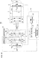
- the power conversion unit includes an inverter 2 having a full-bridge configuration, a transformer 5, a rectification circuit 6, and an output smoothing filter 7.
- a DC power supply 11 is connected to the input side of the inverter 2 of the power conversion unit, and a load 12 is connected to the output side of the output smoothing filter 7.
- the detection/control unit includes an input detection unit 8, an output detection unit 9, and a control unit 10.
- the inverter 2 converts DC voltage of the DC power supply 11 to high-frequency AC voltage, and outputs the high-frequency AC voltage to the transformer 5.
- the transformer 5 keeps isolation between the inverter 2 and the rectification circuit 6, and converts output voltage of the inverter 2 to high-frequency AC voltage having a predetermined peak value.
- the rectification circuit 6 rectifies the high-frequency AC voltage output from the transformer 5.
- the output smoothing filter 7 removes a high-frequency component of the voltage output from the rectification circuit 6, and supplies DC power to the load 12.
- the inverter 2 having a full-bridge configuration is formed by connecting, in parallel, a first leg 3 and a second leg 4 each having switching elements connected in series.
- the second leg 4 has an upper arm 4U and a lower arm 4L connected in series.
- the upper arm 4U has a switching element S3 and a feedback diode D3 connected in antiparallel to the switching element S3.
- the lower arm 4L has a switching element S4 and a feedback diode D4 connected in antiparallel to the switching element S4.
- connection point between the upper arm 3U and the lower arm 3L of the first leg 3, and the connection point between the upper arm 4U and the lower arm 4L of the second leg 4, serve as output terminals of the inverter 2.
- Voltage (VINV) output at the output terminals of the inverter 2 is applied to a primary coil of the transformer 5.
- the rectification circuit 6 composed of diodes D5, D6, D7, D8 is connected to a secondary coil of the transformer 5.
- the output smoothing filter 7 composed of an inductor 71 and a capacitor 72 is connected to output terminals of the rectification circuit 6.
- the load 12 is connected to output of the output smoothing filter 7.
- PWM pulse width modulation
- phase shift control soft switching type
- PWM control hard switching type
- IGBT insulated gate bipolar transistors
- MOSFET metal oxide semiconductor field effect transistors
- D1 to D4 diodes included in IGBTs or MOSFETs may be used, or separate diodes may be provided externally.
- the control unit 10 includes a duty calculator 21, a turn-on phase calculator 22, and a PWM calculator 23.
- duty D Ton/Ts and does not become 0.5 or greater.
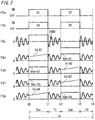
- F2c indicates output voltage (VINV) of the inverter 2 which is voltage input to the transformer 5.
- the voltages across the terminals (drain-source voltages) Vds-S1, Vds-S2, Vds-S3, and Vds-S4 of the switching elements S1 to S4 are indicated by solid lines. Further, total currents Id-Q1, Id-Q2, Id-Q3, and Id-Q4 of currents flowing through the switching elements S1 to S4 and the feedback diodes D1 to D4 of the respective arms are indicated by broken lines.
- t0 to t4 indicate times at which the switching elements S1 to S4 are switched from ON to OFF or from OFF to ON.
- Vds indicates drain voltage of each switching element S1 to S4 with a source potential thereof as a reference
- Id indicates current of each switching element, where the direction of the current flowing inward from the drain is defined as positive.
- a period from t0 to t4 is one switching cycle which is a repetitive cycle of PWM control, and the length thereof is defined as Ts.
- the length of a period from t0 to t1 and the length of a period from t2 to t3 are set to be equal to each other, and this period length is defined as Ton.
- T1 first power non-transmission period
- T2 second power non-transmission period
- a period from t0 to t1 may be referred to as a first power transmission period, and a period from t2 to t3 may be referred to as a second power transmission period.
- the switching element S1 and the switching element S4 are turned on in a voltage applied state, whereby the drain-source voltages thereof are shifted to 0 V. Thus, hard switching is performed and switching loss occurs.
- output voltage (VINV) of the inverter 2 is output in a direction of an arrow in FIG. 1 , and power is supplied to the load 12.
- the switching element S1 and the switching element S4 are turned off in a current conducting state, whereby the currents are interrupted. Thus, hard switching is performed and switching loss occurs.
- the voltage waveform between the drain and the source of each switching element S1 to S4 becomes a waveform in which the resonant voltage is superimposed on half of the voltage Vdc of the DC power supply 11.
- the switching elements S1 to S4 are OFF, power is not supplied from the DC power supply 11, and power is transferred between the transformer 5 and the switching elements S1 to S4 by resonance.
- the switching element S2 of the lower arm 3L of the first leg 3 and the switching element S3 of the upper arm 4U of the second leg 4 are turned on.
- the switching element S2 and the switching element S3 are turned on in a voltage applied state, whereby the drain-source voltages thereof are shifted to 0 V. Thus, hard switching is performed and switching loss occurs.
- the output voltage (VINV) of the inverter 2 is output in an opposite direction of the arrow in FIG. 1 , and power is supplied to the load 12.
- the switching element S2 and the switching element S3 are turned off in a current conducting state, whereby the currents are interrupted. Thus, hard switching is performed and switching loss occurs.
- time t4 After time t4, the operation described above is repeated. That is, time t4 in FIG. 2 will be replaced with time t0.
- switching loss in turn-on operation at times t0 and t2 is proportional to the drain-source voltage immediately before the turn-on operation. Therefore, the switching loss varies depending on the phase of the resonant voltage. For example, as compared to the case where switching is performed when resonant voltage in an ideal state is Vdc/2, turn-on loss decreases if switching is performed at a local minimum point of the resonant voltage, and turn-on loss increases if switching is performed at a local maximum point of the resonant voltage.
- the size of a cooling device is determined so as to allow heat dissipation under a maximum loss condition. Therefore, it is necessary to design a cooling device in consideration of the maximum value of switching loss that varies. Thus, the size of the cooling device is increased, leading to a problem such as apparatus size increase and cost increase.
- T1 first power non-transmission period
- T2 second power non-transmission period
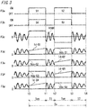
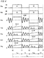
- FIG. 3 and FIG. 4 show time charts corresponding to respective switching patterns of the power conversion device 1 according to the present Embodiment 1.
- FIG. 3 shows the case where T1 (first power non-transmission period) is set to be shorter than T2 (second power non-transmission period).
- FIG. 4 shows the case where T1 (first power non-transmission period) is set to be longer than T2 (second power non-transmission period).
- T1 and T2 different from each other, it is possible to reduce the drain-source voltages of the switching elements S1, S4 at time t0 or the switching elements S2, S3 at time t2, as compared to the case where T1 and T2 are equal to each other.
- a dead time is considered.
- the initial value of time t2 is set at a time obtained by adding a dead time to time t1.
- the turn-on phase is advanced or delayed by a predetermined unit time every switching cycle.
- Tref T1 + T2.
- T1 first power non-transmission period
- T2 second power non-transmission period
- the predetermined unit time is set to be shorter than the cycle of the waveform of resonant voltage between the drain and the source of each switching element S1 to S4, which occurs during T1 (first power non-transmission period) and T2 (second power non-transmission period) as described above.
- T1 (first power non-transmission period) is increased from the length of the dead time to the length of (Ts - 2Ton - dead time), and then is decreased to the length of the dead time.
- T2 (second power non-transmission period) is increased from the length of the dead time to the length of (Ts - 2Ton - dead time), and then is decreased to the length of the dead time.
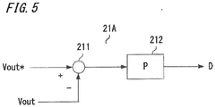
- FIG. 5 shows a block diagram of a duty calculator 21A.
- the duty calculator 21A includes an adder/subtractor 211 and a proportional controller 212.
- a deviation between a voltage detection value Vout of the output detection unit 9 and a predetermined load voltage target value Vout* is subjected to proportional (P) control, thereby calculating the duty D.
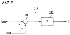
- FIG. 6 shows a block diagram of a duty calculator 21B.
- the duty calculator 21B includes an adder/subtractor 211 and a proportional controller 212.
- the duty D is calculated on the basis of a deviation between a current detection value lout of the output detection unit 9 and a load current target value Iout*.
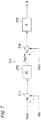
- FIG. 7 shows a block diagram of a duty calculator 21C.
- the duty calculator 21C includes adder/subtractors 211, 214, a proportional integral controller 213, and a proportional controller 215.
- the DC power supply 11 is a current source such as an AC/DC converter
- a deviation between a voltage detection value Vdc of the input detection unit 8 and a power supply voltage target value Vdc* is subjected to proportional integral control, thereby calculating a load current target value Iout*.
- the duty D is calculated on the basis of a deviation between the calculated load current target value Iout* and a current detection value lout of the output detection unit 9.
- the duty D may be calculated on the basis of current Idc of the DC power supply 11 which is a detection value of the input detection unit 8 and a
- DC power supply current target value Idc* which detection value should be used for calculating the duty D may be determined on the basis of what type of load the load 12 is.
- the duty D may be determined on the basis of the current detection value of the output detection unit 9, and if the load requires constant voltage, the duty D may be determined on the basis of the voltage detection value of the output detection unit 9.
- the turn-on phase range is calculated, and then a carrier CarA synchronized with a reference carrier CarS, and a carrier CarB having a phase difference from the reference carrier CarS within the turn-on phase range, are calculated.
- the carrier phase calculator 221 provides the phase difference from the reference carrier CarS, to the carrier CarB.
- the multiplier 225 calculates Ton, i.e., a minimum value (t2min) of t2, on the basis of the duty D which is the calculation result from the duty calculator 21 and the switching cycle Ts. Further, the adder/subtractor 226 calculates a maximum value (t2max) of t2. Thus, the turn-on phase range is calculated.
- the carrier phase calculator 221 changes the turn-on phase within the calculated turn-on phase range (t2min to t2max) every switching cycle.
- the phase of the carrier CarB is advanced or delayed by the predetermined unit time every switching cycle, whereby the turn-on phase is controlled.
- FIG. 9 shows a block diagram of an example of the PWM calculator 23.
- the PWM calculator 23 includes comparators 231, 232, AND gates 233, and delay devices 234.
- the PWM calculator 23 calculates and generates PWM signals for the gates of the switching elements S1 to S4 on the basis of the duty D which is the calculation result from the duty calculator 21 and the carriers CarA, CarB which are the calculation result from the turn-on phase calculator 22.
- the carrier CarA and the carrier CarB are input to the comparators 231, 232 respectively so as to be compared with the duty D, whereby pulse waveforms are generated.
- the PWM signals to be output to the switching elements S1, S4 are generated using the AND gates 233 and the delay devices 234.
- the PWM signals for the switching elements S1 to S4 are generated with a predetermined dead time Td provided thereto.
- the voltage at the time of turning on is averaged through a plurality of switching cycles. Therefore, it is not necessary to perform adjustment in consideration of individual variations in the leakage inductance and the parasitic capacitance of the transformer and the parasitic capacitances of the switching elements.
- the rectification circuit 6 (6A) and the output smoothing filter 7 have been described as separate components. However, the components of the output smoothing filter may be incorporated into the rectification circuit so that the entirety is integrated in the rectification circuit.
- the lengths of the first power transmission period and the second power transmission period are set to be equal to each other.
- the amplitude during the first power transmission period and the amplitude during the second power transmission period are different from each other so that biased magnetization occurs in the transformer 5A
- the lengths of the first power transmission period and the second power transmission period may be set to be different from each other.
- the turn-on voltages of the switching elements S1 to S4 can be averaged through a plurality of switching cycles.
- the thermal time constant of the cooling device is greater than the switching cycle. Therefore, loss in the switching elements is averaged and the maximum loss that should be considered in designing the cooling device can be suppressed.
- the controller and the cooling device are downsized, whereby a small-sized power conversion device can be realized.
- a period from when the switching elements at the first diagonal positions in the full-bridge inverter are turned off at the same time to when the switching elements at the second diagonal positions are turned on at the same time is defined as T1 (first power non-transmission period)
- T2 second power non-transmission period
- a period (first power transmission period) during which the switching elements at the first diagonal positions are turned on at the same time and a period (second power transmission period) during which the switching elements at the second diagonal positions are turned on at the same time are set to be equal to each other (Ton)
- the switching cycle Ts and Ton are constant.
- the control unit repeats sweeping of T1 (first power non-transmission period) in a range from 0 to (Ts - 2Ton) at certain time intervals in respective switching cycles.
- T1 first power non-transmission period
- Ts - 2Ton turn-on voltages of the switching elements
- the turn-on voltages of the switching elements can be averaged through a plurality of switching cycles.
- increase in switching loss is suppressed by a simple control method, whereby the controller and the cooling device can be downsized and thus a small-sized power conversion device can be provided.
- sweeping of T1 is performed in a range from 0 to (Ts - 2Ton), whereby the turn-on voltages of the switching elements are averaged.
- a temperature detection unit for switching elements is provided, and on the basis of temperature detection values about the switching elements, the turn-on phase for the switching elements is changed to search for a point where the temperatures of the switching elements are minimized, thereby searching for the turn-on phase for the switching elements that minimizes turn-on loss in the switching elements.
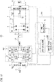
- the power conversion device 100 is roughly composed of a power conversion unit and a detection/control unit.
- the power conversion unit includes the inverter 2 having a full-bridge configuration, the transformer 5, the rectification circuit 6, and the output smoothing filter 7.
- the DC power supply 11 is connected to the input side of the inverter 2 of the power conversion unit, and the load 12 is connected to the output side of the output smoothing filter 7.
- the detection/control unit includes the input detection unit 8, the output detection unit 9, a temperature detection unit 130, and a control unit 110.
- the inverter 2 converts DC voltage of the DC power supply 11 to high-frequency AC voltage, and outputs the high-frequency AC voltage to the transformer 5.
- the transformer 5 keeps isolation between the inverter 2 and the rectification circuit 6, and performs conversion to predetermined high-frequency AC voltage.
- the rectification circuit 6 rectifies the high-frequency AC voltage output from the transformer 5.
- the output smoothing filter 7 removes a high-frequency component of the voltage output from the rectification circuit 6, and supplies DC power to the load 12.
- Embodiment 2 the configuration of the inverter 2 of the power conversion unit in the power conversion device 100 is the same as that in Embodiment 1.
- the power conversion device 100 according to Embodiment 2 includes the input detection unit 8, the output detection unit 9, and the temperature detection unit 130 as detection units.
- the input detection unit 8 is provided in parallel to the DC power supply 11, and detects at least one of voltage Vdc and current Idc of the DC power supply 11.
- the output detection unit 9 is provided in parallel to the load 12, and detects at least one of voltage Vout and current lout of the load.
- the temperature detection unit 130 for detecting the temperatures of the switching elements S1 to S4 is provided.
- the temperatures of all the switching elements S1 to S4 are detected.
- the temperature of one or some of the switching elements may be detected as a representative.
- the control unit 110 includes the duty calculator 21, a turn-on phase calculator 122, and the PWM calculator 23. As described below, a difference between the control unit 110 and the control unit 10 of Embodiment 1 is the turn-on phase calculator 122.
- FIG. 12 shows a block diagram of the turn-on phase calculator 122.
- the turn-on phase calculator 122 includes a carrier phase calculator 221A, a multiplier 225, and an adder/subtractor 226.
- a signal from the temperature detection unit 130 is denoted by Tmp.
- the carrier phase calculator 221A periodically performs sweeping of the turn-on phase within the turn-on phase range, for the carrier CarB. That is, for example, T1 (first power non-transmission period) is increased from 0 to (Ts - 2Ton).
- the carrier phase calculator 221A stores a result of temperature detection at each turn-on phase, and selects the phase of the carrier CarB at which the temperature detection result is minimized.
- a temperature detection result for each turn-on phase may be stored, or only data corresponding to the minimum temperature may be stored.
- a waiting time until the temperatures are saturated may be provided.
- the turn-on phase can be adjusted on the basis of the temperatures. Therefore, it is not necessary to perform adjustment in consideration of individual variations in the leakage inductance and the parasitic capacitance of the transformer and the parasitic capacitances of the switching elements.
- the searching for the turn-on phase that minimizes turn-on loss in the switching elements on the basis of the temperature detection values about the switching elements in the present Embodiment 2 is also applicable to the power conversion device in which a center point is provided to the secondary winding of the transformer and the rectification circuit 6 has a center-tap configuration.
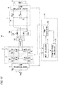
- FIG. 13 is a configuration diagram of the power conversion device
- FIG. 14 which is a block diagram showing the configuration of a control unit (turn-on phase calculator)
- FIG. 15 which is a block diagram showing the configuration of the control unit (duty calculator).
- parts that are the same as or correspond to those in the drawings in embodiments 1 and 2 are denoted by the same reference characters.
- the power conversion device 200 is roughly composed of a power conversion unit and a detection/control unit.
- the power conversion unit includes the inverter 2 having a full-bridge configuration, the transformer 5, the rectification circuit 6, and the output smoothing filter 7.
- the DC power supply 11 is connected to the input side of the inverter 2 of the power conversion unit, and the load 12 is connected to the output side of the output smoothing filter 7.
- the detection/control unit includes the input detection unit 8, the output detection unit 9, and a control unit 210.
- the inverter 2 converts DC voltage of the DC power supply 11 to high-frequency AC voltage, and outputs the high-frequency AC voltage to the transformer 5.
- the transformer 5 keeps isolation between the inverter 2 and the rectification circuit 6, and performs conversion to predetermined high-frequency AC voltage.
- the rectification circuit 6 rectifies the high-frequency AC voltage output from the transformer 5.
- the output smoothing filter 7 removes a high-frequency component of the voltage output from the rectification circuit 6, and supplies DC power to the load 12.
- the power conversion device 200 according to Embodiment 3 includes the input detection unit 8 and the output detection unit 9 as detection units.
- the input detection unit 8 is provided in parallel to the DC power supply 11, and detects at least one of voltage Vdc and current Idc of the DC power supply 11.
- the output detection unit 9 is provided in parallel to the load 12, and detects at least one of voltage Vout and current lout of the load.
- the control unit 210 includes the duty calculator 21, a turn-on phase calculator 222, and the PWM calculator 23. As described below, a difference between the control unit 210 and the control unit 110 of Embodiment 2 is the turn-on phase calculator 222.
- the temperatures of the switching elements S1 to S4 detected by the temperature detection unit 130 are output to the turn-on phase calculator 122.
- the voltage/current value detected by the input detection unit 8 or the output detection unit 9 is output also to the turn-on phase calculator 222.
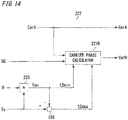
- FIG. 14 shows a block diagram of the turn-on phase calculator 222.
- the turn-on phase calculator 222 includes a carrier phase calculator 221B, a multiplier 225, and an adder/subtractor 226.
- a signal from the input detection unit 8 or the output detection unit 9 is denoted by SG.
- the turn-on phase calculator 222 calculates the turn-on phase range on the basis of the duty D which is a calculation result from the duty calculator 21 and the switching cycle Ts, and calculates a carrier CarA synchronized with the reference carrier CarS within the turn-on phase range and a carrier CarB having a phase difference from the reference carrier CarS within the turn-on phase range.
- a carrier phase calculator 221B calculates the turn-on phase.
- searching for a point where the input current detection value is minimized is performed using the input current detection value detected by the input detection unit 8.
- a voltage source is on the input side and a voltage source load such as a battery is on the output side.
- the turn-on phase calculator 222 controls the turn-on phase and searches for a point where the input current is minimized, on the basis of the input current detection value of the input detection unit 8.
- the carrier phase calculator 221B periodically performs sweeping of the turn-on phase within the turn-on phase range, for the carrier CarB. That is, for example, T1 (first power non-transmission period) is increased from 0 to (Ts - 2Ton).
- the power conversion device 200 according to Embodiment 3 has been described using the case where a voltage source is on the input side and a voltage source load such as a battery is on the output side.
- the DC power supply 11 is a constant power source such as an AC/DC converter and a voltage source load such as a battery is on the output side, if the output current becomes great, switching loss is reduced.
- the power conversion device In the power conversion device according to the present Embodiment 3, it is possible to search for a point that minimizes switching loss in the switching elements, on the basis of the input current detection value, for example. Therefore, it is not necessary to perform adjustment in consideration of individual variations in the leakage inductance and the parasitic capacitance of the transformer and the parasitic capacitances of the switching elements.
- the turn-on phase for the switching elements is changed to search for a point where the detection input current of the input detection unit is minimized, thereby searching for the turn-on phase for the switching elements that minimizes turn-on loss in the switching elements. Therefore, as in the power conversion device according to Embodiment 1, increase in switching loss is suppressed by a simple control method, whereby the controller and the cooling device can be downsized and thus a small-sized power conversion device can be provided.
- the power conversion device 300 is roughly composed of a power conversion unit and a detection/control unit.
- the detection/control unit includes the input detection unit 8, the output detection unit 9, and a control unit 310.
- Embodiment 4 the configuration and the operation of the inverter 2 of the power conversion unit in the power conversion device 300 are the same as those in Embodiment 2.
- Embodiment 2 Differences from Embodiment 2, i.e., differences in the configuration and the operation of the detection/control unit in the power conversion device 300, will be mainly described.
- the power conversion device 300 according to Embodiment 4 includes the input detection unit 8, the output detection unit 9, and the temperature detection unit 130 as detection units.
- the input detection unit 8 is provided in parallel to the DC power supply 11, and detects at least one of voltage Vdc and current Idc of the DC power supply 11.
- the output detection unit 9 is provided in parallel to the load 12, and detects at least one of voltage Vout and current lout of the load.
- the temperature detection unit 130 for detecting the temperatures of the switching elements S1 to S4 is provided.
- the control unit 310 includes the duty calculator 21, a turn-on phase calculator 322, and the PWM calculator 23. As described below, a difference between the control unit 310 and the control unit 210 of Embodiment 2 is the turn-on phase calculator 322.
- FIG. 17 shows a block diagram of the turn-on phase calculator 322.
- the turn-on phase calculator 322 includes the carrier phase calculator 221A, the multiplier 225, the adder/subtractor 226, and a high-pass filter 327.
- a signal from the temperature detection unit 130 is denoted by Tmp.
- the temperature detection unit 130 detects the temperatures of the switching elements S1 to S4 and outputs the temperatures to the turn-on phase calculator 322. However, unlike Embodiment 2, the signal (Tmp) from the temperature detection unit 130 is input to the carrier phase calculator 221A via the high-pass filter 327.
- the turn-on phase calculator 322 calculates the turn-on phase range on the basis of the duty D which is a calculation result from the duty calculator 21 and the switching cycle Ts, and calculates a carrier CarA synchronized with the reference carrier CarS within the turn-on phase range, and a carrier CarB having a phase difference from the reference carrier CarS within the turn-on phase range.
- the carrier phase calculator 221A calculates a turn-on phase.
- the carrier phase calculator 221A periodically performs sweeping of the turn-on phase within the turn-on phase range, for the carrier CarB. That is, for example, T1 (first power non-transmission period) is increased from 0 to (Ts - 2Ton).
- the carrier phase calculator 221A stores a temperature detection result that has passed through the high-pass filter 327, for each turn-on phase, and selects the phase of the carrier CarB at which the temperature detection result is minimized.
- a temperature detection result for each turn-on phase may be stored, or only data corresponding to the minimum temperature may be stored.
- a large-capacity battery such as an on-vehicle charger mounted to an electric vehicle (EV), plug-in hybrid electric vehicle (PHEV), or the like
- EV electric vehicle
- PHEV plug-in hybrid electric vehicle
- the temperatures of the switching elements also gradually change.
- resonant oscillation during the power non-transmission period has a high frequency at MHz level, and the time constant of temperature change is shorter as compared with the time constant of temperature change due to change in battery voltage.
- the high-pass filter circuit 327 newly provided in the present Embodiment 4 makes it possible to remove temperature change due to battery voltage increase and detect only temperature change due to resonant oscillation. Therefore, it is possible to search for a point that minimizes switching loss, with high accuracy.
- a power conversion device is configured such that capacitors are added in parallel to the switching elements of the inverter in the power conversion unit or an inductor is added to the primary winding of the transformer in order to ease searching for a point that minimizes switching loss, as compared to embodiments 2 to 4.
- FIG. 18 is a configuration diagram of the power conversion device.
- parts that are the same as or correspond to those in the drawings in embodiments 1 and 3 are denoted by the same reference characters.
- a power conversion device 400 is roughly composed of a power conversion unit and a detection/control unit.
- the power conversion unit includes an inverter 402 having a full-bridge configuration, the transformer 5, the rectification circuit 6, the output smoothing filter 7, and an inductor L1 connected in series to the primary winding of the transformer 5.
- the DC power supply 11 is connected to the input side of the inverter 402 of the power conversion unit, and the load 12 is connected to the output side of the output smoothing filter 7.
- the detection/control unit includes the input detection unit 8, the output detection unit 9, and the control unit 210.
- Embodiment 5 the basic configuration and operation of the inverter 402 of the power conversion unit in the power conversion device 500 are the same as those in Embodiment 3.
- Connecting the capacitors C1 to C4 in parallel to the switching elements S1 to S4 of the inverter 402 and connecting the inductor L1 in series to the primary winding of the transformer 5 enables reduction of the frequency of resonant oscillation occurring during the first power non-transmission period and the second power non-transmission period, thereby easing searching for a point that minimizes switching loss.
- capacitors C1 to C4 or the inductor L1 may be added.
- a capacitor may be connected in parallel to one or more of the switching elements S1 to S4.
- capacitors may be added to the switching elements of the upper arms (3U, 4U) or the lower arms (3L, 4L).
- capacitors may be added to the switching elements of the first leg 3 or the second leg 4.
- capacitors may be added to only a diagonal pair of elements, i.e., the switching elements S1 and S4 or the switching elements S2 and S3.
- the inductor L1 may be connected in series to the secondary winding of the transformer 5, or may be provided on both of the primary side and the secondary side.
- the present invention enables size reduction of the controller and the cooling device by suppressing increase in switching loss by a simple control method, and therefore is widely applicable to power conversion devices.
Landscapes
- Engineering & Computer Science (AREA)
- Power Engineering (AREA)
- Inverter Devices (AREA)
- Dc-Dc Converters (AREA)
Applications Claiming Priority (2)
| Application Number | Priority Date | Filing Date | Title |
|---|---|---|---|
| JP2017073382 | 2017-04-03 | ||
| PCT/JP2017/037981 WO2018185962A1 (ja) | 2017-04-03 | 2017-10-20 | 電力変換装置 |
Publications (3)
| Publication Number | Publication Date |
|---|---|
| EP3609062A1 true EP3609062A1 (de) | 2020-02-12 |
| EP3609062A4 EP3609062A4 (de) | 2020-04-08 |
| EP3609062B1 EP3609062B1 (de) | 2026-03-04 |
Family
ID=63712540
Family Applications (1)
| Application Number | Title | Priority Date | Filing Date |
|---|---|---|---|
| EP17904457.3A Active EP3609062B1 (de) | 2017-04-03 | 2017-10-20 | Stromwandlungsvorrichtung |
Country Status (5)
| Country | Link |
|---|---|
| US (1) | US11563368B2 (de) |
| EP (1) | EP3609062B1 (de) |
| JP (1) | JP6381853B1 (de) |
| CN (1) | CN110447163B (de) |
| WO (1) | WO2018185962A1 (de) |
Families Citing this family (3)
| Publication number | Priority date | Publication date | Assignee | Title |
|---|---|---|---|---|
| JP6913599B2 (ja) * | 2017-10-17 | 2021-08-04 | 日立Astemo株式会社 | 制御装置 |
| US20240235403A1 (en) * | 2021-06-30 | 2024-07-11 | Mitsubishi Electric Corporation | Power conversion device |
| CN115769478B (zh) * | 2022-05-25 | 2026-03-24 | 深圳市富兰瓦时技术有限公司 | 软启动方法、功率转换系统及户用储能系统 |
Family Cites Families (19)
| Publication number | Priority date | Publication date | Assignee | Title |
|---|---|---|---|---|
| JPH10174205A (ja) | 1996-12-09 | 1998-06-26 | Yamaha Motor Co Ltd | 給電装置 |
| JP3431537B2 (ja) | 1999-05-31 | 2003-07-28 | 株式会社デンソー | 電気自動車用電源装置の充電制御方法 |
| JP2002238257A (ja) | 2001-02-06 | 2002-08-23 | Toshiba Corp | 共振型dc−dcコンバータの制御方法 |
| JP2004040983A (ja) | 2002-07-08 | 2004-02-05 | Onkyo Corp | スイッチング電源回路およびこの電源回路を備えたスイッチングレギュレータ |
| US20080088268A1 (en) * | 2004-09-24 | 2008-04-17 | Rohm Co., Ltd. | Fan Motor Drive Device and Cooler |
| JP4735013B2 (ja) | 2005-04-15 | 2011-07-27 | パナソニック株式会社 | 電力変換装置 |
| WO2007148271A2 (en) * | 2006-06-20 | 2007-12-27 | Koninklijke Philips Electronics N.V. | Method for operating a resonant power converter |
| EP2232669B1 (de) * | 2008-01-07 | 2019-12-04 | Philips IP Ventures B.V. | Induktive stromversorgung mit taktzyklussteuerung |
| JP5560664B2 (ja) | 2009-11-05 | 2014-07-30 | 富士電機株式会社 | 直流−直流変換回路の制御方法 |
| CN101795076B (zh) * | 2009-01-29 | 2015-04-15 | 富士电机株式会社 | 功率变换器以及控制功率变换器的方法 |
| JP5491809B2 (ja) * | 2009-09-25 | 2014-05-14 | パナソニック株式会社 | 系統連系インバータ装置 |
| JP5856391B2 (ja) * | 2010-07-01 | 2016-02-09 | キヤノン株式会社 | Dc/dcコンバータ及び電子機器 |
| US9787190B2 (en) * | 2011-04-18 | 2017-10-10 | Mitsubishi Electric Corporation | Power conversion device and in-vehicle power supply device equipped with same |
| ITTO20110863A1 (it) | 2011-09-28 | 2013-03-29 | Magneti Marelli Spa | Procedimento di conversione dc-dc con modulazione phase-shift e relativo apparato di conversione |
| JP5866614B1 (ja) | 2014-12-05 | 2016-02-17 | パナソニックIpマネジメント株式会社 | スイッチング電源装置 |
| JP6427432B2 (ja) | 2015-02-02 | 2018-11-21 | 株式会社ダイヘン | 電源装置及び溶接用電源装置 |
| US10211719B2 (en) * | 2015-03-03 | 2019-02-19 | Mitsubishi Electric Corporation | Power converter |
| JP6129240B2 (ja) | 2015-06-03 | 2017-05-17 | 三菱電機株式会社 | 電力変換装置および電力変換方法 |
| CN205356156U (zh) * | 2016-02-19 | 2016-06-29 | 襄阳九鼎昊天环保设备有限公司 | 基于dsp的智能型高频高压直流电源 |
-
2017
- 2017-10-20 US US16/479,703 patent/US11563368B2/en active Active
- 2017-10-20 WO PCT/JP2017/037981 patent/WO2018185962A1/ja not_active Ceased
- 2017-10-20 EP EP17904457.3A patent/EP3609062B1/de active Active
- 2017-10-20 CN CN201780088696.XA patent/CN110447163B/zh active Active
- 2017-10-20 JP JP2018510145A patent/JP6381853B1/ja active Active
Also Published As
| Publication number | Publication date |
|---|---|
| US11563368B2 (en) | 2023-01-24 |
| CN110447163A (zh) | 2019-11-12 |
| EP3609062A4 (de) | 2020-04-08 |
| WO2018185962A1 (ja) | 2018-10-11 |
| JPWO2018185962A1 (ja) | 2019-04-11 |
| JP6381853B1 (ja) | 2018-08-29 |
| EP3609062B1 (de) | 2026-03-04 |
| CN110447163B (zh) | 2021-01-15 |
| US20200266699A1 (en) | 2020-08-20 |
Similar Documents
| Publication | Publication Date | Title |
|---|---|---|
| JP5558631B2 (ja) | 電力変換装置およびそれを備えた車載電源装置 | |
| US9025345B2 (en) | Power supply apparatus | |
| US10926649B2 (en) | Method to reduce losses in a high voltage DC link converter | |
| US10211719B2 (en) | Power converter | |
| US11056979B2 (en) | Power conversion apparatus | |
| US20160072387A1 (en) | Dc/dc converter | |
| US11025174B2 (en) | Converter with soft switching function | |
| US20100220500A1 (en) | Power converter and method for controlling power converter | |
| US9871455B2 (en) | Current resonance type power supply device | |
| US11095219B2 (en) | Converter with soft switching function | |
| JP5893089B2 (ja) | 直流変換装置の制御方法 | |
| US20150256089A1 (en) | Power conversion apparatus | |
| US10027234B2 (en) | Power conversion device for performing power conversion between DC and DC by controlling switching of a semiconductor switching element | |
| JP2015070716A (ja) | Dc/dcコンバータ | |
| EP2814165B1 (de) | Gleichstromversorgung | |
| EP3609062B1 (de) | Stromwandlungsvorrichtung | |
| US10924000B2 (en) | DC-DC converter with reduced ripple | |
| US20100226152A1 (en) | Inverter | |
| KR20150070898A (ko) | 직류-직류 컨버터 및 이의 스위칭 방법 | |
| JP6132882B2 (ja) | 電力変換装置 | |
| US20180219471A1 (en) | Power supply device | |
| JP2022121050A (ja) | 電力変換装置 | |
| WO2017216828A1 (ja) | 電力変換装置 |
Legal Events
| Date | Code | Title | Description |
|---|---|---|---|
| STAA | Information on the status of an ep patent application or granted ep patent |
Free format text: STATUS: THE INTERNATIONAL PUBLICATION HAS BEEN MADE |
|
| PUAI | Public reference made under article 153(3) epc to a published international application that has entered the european phase |
Free format text: ORIGINAL CODE: 0009012 |
|
| STAA | Information on the status of an ep patent application or granted ep patent |
Free format text: STATUS: REQUEST FOR EXAMINATION WAS MADE |
|
| 17P | Request for examination filed |
Effective date: 20190926 |
|
| AK | Designated contracting states |
Kind code of ref document: A1 Designated state(s): AL AT BE BG CH CY CZ DE DK EE ES FI FR GB GR HR HU IE IS IT LI LT LU LV MC MK MT NL NO PL PT RO RS SE SI SK SM TR |
|
| AX | Request for extension of the european patent |
Extension state: BA ME |
|
| A4 | Supplementary search report drawn up and despatched |
Effective date: 20200311 |
|
| RIC1 | Information provided on ipc code assigned before grant |
Ipc: H02M 7/48 20070101ALI20200305BHEP Ipc: H02M 3/337 20060101ALI20200305BHEP Ipc: H02M 1/08 20060101ALI20200305BHEP Ipc: H02M 1/38 20070101ALI20200305BHEP Ipc: H02M 1/00 20060101ALN20200305BHEP Ipc: H02M 3/28 20060101AFI20200305BHEP |
|
| DAV | Request for validation of the european patent (deleted) | ||
| DAX | Request for extension of the european patent (deleted) | ||
| STAA | Information on the status of an ep patent application or granted ep patent |
Free format text: STATUS: EXAMINATION IS IN PROGRESS |
|
| 17Q | First examination report despatched |
Effective date: 20210415 |
|
| GRAP | Despatch of communication of intention to grant a patent |
Free format text: ORIGINAL CODE: EPIDOSNIGR1 |
|
| STAA | Information on the status of an ep patent application or granted ep patent |
Free format text: STATUS: GRANT OF PATENT IS INTENDED |
|
| RIC1 | Information provided on ipc code assigned before grant |
Ipc: H02M 3/28 20060101AFI20250923BHEP Ipc: H02M 7/48 20070101ALI20250923BHEP Ipc: H02M 1/08 20060101ALI20250923BHEP Ipc: H02M 1/38 20070101ALI20250923BHEP Ipc: H02M 3/337 20060101ALI20250923BHEP Ipc: H02M 1/00 20060101ALN20250923BHEP |
|
| INTG | Intention to grant announced |
Effective date: 20251002 |
|
| RIN1 | Information on inventor provided before grant (corrected) |
Inventor name: TAKAHARA, TAKAAKI Inventor name: MIZUTANI, HIROTO Inventor name: KONDO, RYOTA Inventor name: MURAKAMI, SATOSHI Inventor name: IWABUKI, HIROYASU Inventor name: HAYASE, KEI |
|
| GRAS | Grant fee paid |
Free format text: ORIGINAL CODE: EPIDOSNIGR3 |
|
| GRAA | (expected) grant |
Free format text: ORIGINAL CODE: 0009210 |
|
| STAA | Information on the status of an ep patent application or granted ep patent |
Free format text: STATUS: THE PATENT HAS BEEN GRANTED |
|
| AK | Designated contracting states |
Kind code of ref document: B1 Designated state(s): AL AT BE BG CH CY CZ DE DK EE ES FI FR GB GR HR HU IE IS IT LI LT LU LV MC MK MT NL NO PL PT RO RS SE SI SK SM TR |
|
| REG | Reference to a national code |
Ref country code: CH Ref legal event code: F10 Free format text: ST27 STATUS EVENT CODE: U-0-0-F10-F00 (AS PROVIDED BY THE NATIONAL OFFICE) Effective date: 20260304 Ref country code: GB Ref legal event code: FG4D |
|
| REG | Reference to a national code |
Ref country code: IE Ref legal event code: FG4D |
|
| REG | Reference to a national code |
Ref country code: DE Ref legal event code: R096 Ref document number: 602017094195 Country of ref document: DE |